US9123900B2 - Host material and organic light emitting display device using the same - Google Patents
Host material and organic light emitting display device using the same Download PDFInfo
- Publication number
- US9123900B2 US9123900B2 US13/688,479 US201213688479A US9123900B2 US 9123900 B2 US9123900 B2 US 9123900B2 US 201213688479 A US201213688479 A US 201213688479A US 9123900 B2 US9123900 B2 US 9123900B2
- Authority
- US
- United States
- Prior art keywords
- host material
- group
- display device
- emitting display
- light emitting
- Prior art date
- Legal status (The legal status is an assumption and is not a legal conclusion. Google has not performed a legal analysis and makes no representation as to the accuracy of the status listed.)
- Active, expires
Links
- 0 *[S+](*)(*)[n]1c(cc(-c2ccccc2-2)c-2c2)c2c2c1cccc2 Chemical compound *[S+](*)(*)[n]1c(cc(-c2ccccc2-2)c-2c2)c2c2c1cccc2 0.000 description 23
- OGAOBTUHOOHQGY-UHFFFAOYSA-N C[Si](C)(C)N1C2=C(C=CC=C2)C2=C1C=C1C(=C2)C2=C1C=CC=C2 Chemical compound C[Si](C)(C)N1C2=C(C=CC=C2)C2=C1C=C1C(=C2)C2=C1C=CC=C2 OGAOBTUHOOHQGY-UHFFFAOYSA-N 0.000 description 5
- DTZBHGZABREPNO-UHFFFAOYSA-N C[Si](C)(C)N1C2=C(C=C3C(=C2)C2=C(C=CC=C2)S3(=O)=O)C2=C1/C=C\C=C/2.C[Si](C)(C)N1C2=C(C=C3C(=C2)C2=C(C=CC=C2)S3=O)C2=C1/C=C\C=C/2.C[Si](C)(C)N1C2=C(C=C3OC4=C(C=CC=C4)C3=C2)C2=C1/C=C\C=C/2.C[Si](C)(C)N1C2=C(C=C3SC4=C(C=CC=C4)C3=C2)C2=C1/C=C\C=C/2.C[Si](C)(C)N1C2=CC=CC=C2C2=C1C1=C(C=C2)C2=C(C=CC=C2)O1.C[Si](C)(C)N1C2=CC=CC=C2C2=C1C1=C(C=C2)C2=C(C=CC=C2)S1 Chemical compound C[Si](C)(C)N1C2=C(C=C3C(=C2)C2=C(C=CC=C2)S3(=O)=O)C2=C1/C=C\C=C/2.C[Si](C)(C)N1C2=C(C=C3C(=C2)C2=C(C=CC=C2)S3=O)C2=C1/C=C\C=C/2.C[Si](C)(C)N1C2=C(C=C3OC4=C(C=CC=C4)C3=C2)C2=C1/C=C\C=C/2.C[Si](C)(C)N1C2=C(C=C3SC4=C(C=CC=C4)C3=C2)C2=C1/C=C\C=C/2.C[Si](C)(C)N1C2=CC=CC=C2C2=C1C1=C(C=C2)C2=C(C=CC=C2)O1.C[Si](C)(C)N1C2=CC=CC=C2C2=C1C1=C(C=C2)C2=C(C=CC=C2)S1 DTZBHGZABREPNO-UHFFFAOYSA-N 0.000 description 2
- XPQMLNOXDVFVGS-UHFFFAOYSA-N C[Si](C)(C)N1C2=CC=CC=C2C2=C1C1=C(C=C2)C2=C(C=CC=C2)S1(=O)=O.C[Si](C)(C)N1C2=CC=CC=C2C2=C1C1=C(C=C2)C2=C(C=CC=C2)S1=O Chemical compound C[Si](C)(C)N1C2=CC=CC=C2C2=C1C1=C(C=C2)C2=C(C=CC=C2)S1(=O)=O.C[Si](C)(C)N1C2=CC=CC=C2C2=C1C1=C(C=C2)C2=C(C=CC=C2)S1=O XPQMLNOXDVFVGS-UHFFFAOYSA-N 0.000 description 2
- MZQOJTMCASBQAQ-UHFFFAOYSA-N C.C1=CC=C([Si](C2=CC=CC=C2)(C2=CC=CC=C2)N2C3=CC4=C(C=C3C3=C2C=CC=C3)N([Si](C2=CC=CC=C2)(C2=CC=CC=C2)C2=CC=CC=C2)C2=C4/C=C\C=C/2)C=C1.Cl[Si](C1=CC=CC=C1)(C1=CC=CC=C1)C1=CC=CC=C1.[C+]1=CC2=C(C=C1)C1=CC3=C(C=C1N2)C1=C(/C=C\C=C/1)C3 Chemical compound C.C1=CC=C([Si](C2=CC=CC=C2)(C2=CC=CC=C2)N2C3=CC4=C(C=C3C3=C2C=CC=C3)N([Si](C2=CC=CC=C2)(C2=CC=CC=C2)C2=CC=CC=C2)C2=C4/C=C\C=C/2)C=C1.Cl[Si](C1=CC=CC=C1)(C1=CC=CC=C1)C1=CC=CC=C1.[C+]1=CC2=C(C=C1)C1=CC3=C(C=C1N2)C1=C(/C=C\C=C/1)C3 MZQOJTMCASBQAQ-UHFFFAOYSA-N 0.000 description 1
- ORANWMDRHITLIK-UHFFFAOYSA-N C/C1=C/C=C(/[Si](C)(C)C)C2=CC=CC=C21.CC1=C([Si](C)(C)C)C=CC=C1.CC1=CC([Si](C)(C)C)=CC=C1.CC1=CC=C(C2=CC=C([Si](C)(C)C)C=C2)C=C1.CC1=CC=C([Si](C)(C)C)C=C1 Chemical compound C/C1=C/C=C(/[Si](C)(C)C)C2=CC=CC=C21.CC1=C([Si](C)(C)C)C=CC=C1.CC1=CC([Si](C)(C)C)=CC=C1.CC1=CC=C(C2=CC=C([Si](C)(C)C)C=C2)C=C1.CC1=CC=C([Si](C)(C)C)C=C1 ORANWMDRHITLIK-UHFFFAOYSA-N 0.000 description 1
- USWCCFZPNQGCEF-UHFFFAOYSA-N C1=CC2=C(C=C1)C1=CC3=C(C=C1N2)C1=C(/C=C\C=C/1)C3.C1=CC=C2C(=C1)C/C=C\2C/C1=C/NC2=C1C=CC=C2.CCOC(OCC)OCC Chemical compound C1=CC2=C(C=C1)C1=CC3=C(C=C1N2)C1=C(/C=C\C=C/1)C3.C1=CC=C2C(=C1)C/C=C\2C/C1=C/NC2=C1C=CC=C2.CCOC(OCC)OCC USWCCFZPNQGCEF-UHFFFAOYSA-N 0.000 description 1
- VYPIKBSTXHFQDD-UHFFFAOYSA-N CC1=C(C(F)(F)F)C=CC=C1.CC1=C(F)C=CC=C1.CC1=CC(C(F)(F)F)=CC=C1.CC1=CC(F)=CC(F)=C1.CC1=CC(F)=CC=C1.CC1=CC=C(C(F)(F)F)C=C1.CC1=CC=C(F)C=C1 Chemical compound CC1=C(C(F)(F)F)C=CC=C1.CC1=C(F)C=CC=C1.CC1=CC(C(F)(F)F)=CC=C1.CC1=CC(F)=CC(F)=C1.CC1=CC(F)=CC=C1.CC1=CC=C(C(F)(F)F)C=C1.CC1=CC=C(F)C=C1 VYPIKBSTXHFQDD-UHFFFAOYSA-N 0.000 description 1
- XTSLTVBPEDHZJR-UHFFFAOYSA-N CC1=C(C(F)(F)F)C=CC=C1F.CC1=C(F)C(F)=CC=C1.CC1=C(F)C=C(F)C=C1.CC1=C(F)C=CC(C#N)=C1.CC1=C(F)C=CC(F)=C1.CC1=CC(F)=C(F)C=C1.COC1=CC=CC(OC)=C1C Chemical compound CC1=C(C(F)(F)F)C=CC=C1F.CC1=C(F)C(F)=CC=C1.CC1=C(F)C=C(F)C=C1.CC1=C(F)C=CC(C#N)=C1.CC1=C(F)C=CC(F)=C1.CC1=CC(F)=C(F)C=C1.COC1=CC=CC(OC)=C1C XTSLTVBPEDHZJR-UHFFFAOYSA-N 0.000 description 1
- WMUDXPCCEQVUGJ-UHFFFAOYSA-N CC1=C(C)C=CC=C1.CC1=C2C=CC=NC2=CC=C1.CC1=CC(C2=CC=CC=N2)=NC(C2=NC=CC=C2)=C1.CC1=CC=C(C)C=C1.CC1=CC=C2N=CC=CC2=C1.CC1=CC=CC(C)=C1.CC1=NC2=CC=CC=C2C=C1.CC1=NC=CS1 Chemical compound CC1=C(C)C=CC=C1.CC1=C2C=CC=NC2=CC=C1.CC1=CC(C2=CC=CC=N2)=NC(C2=NC=CC=C2)=C1.CC1=CC=C(C)C=C1.CC1=CC=C2N=CC=CC2=C1.CC1=CC=CC(C)=C1.CC1=NC2=CC=CC=C2C=C1.CC1=NC=CS1 WMUDXPCCEQVUGJ-UHFFFAOYSA-N 0.000 description 1
- AOBUNCMMGMJNBR-UHFFFAOYSA-N CC1=C(C2=NC=CC=C2)C=CC=C1.CC1=CC(C2=NC=CC=C2)=CC=C1.CC1=CC=C(C2=CC=CC=N2)C=C1.CC1=CN=CC=C1.CC1=CN=CN=C1.CC1=NC=CC=N1 Chemical compound CC1=C(C2=NC=CC=C2)C=CC=C1.CC1=CC(C2=NC=CC=C2)=CC=C1.CC1=CC=C(C2=CC=CC=N2)C=C1.CC1=CN=CC=C1.CC1=CN=CN=C1.CC1=NC=CC=N1 AOBUNCMMGMJNBR-UHFFFAOYSA-N 0.000 description 1
- BRHVBZSMBIZEGA-UHFFFAOYSA-N CC1=CC(C)=C(C)C=C1.CC1=CC(C)=CC(C)=C1.CC1=CC=CC(C)=C1C.CC1=CSC2=C1SC=C2.COC1=C(C)C=CC=C1.COC1=CC=C(C)C=C1.COC1=CC=CC(C)=C1 Chemical compound CC1=CC(C)=C(C)C=C1.CC1=CC(C)=CC(C)=C1.CC1=CC=CC(C)=C1C.CC1=CSC2=C1SC=C2.COC1=C(C)C=CC=C1.COC1=CC=C(C)C=C1.COC1=CC=CC(C)=C1 BRHVBZSMBIZEGA-UHFFFAOYSA-N 0.000 description 1
- NIGJHKRVGFZXHY-UHFFFAOYSA-N CC1=CC(C)=CC(C(F)(F)F)=C1.CC1=CC=C(C(C)(C)C)C=C1.CC1=CC=C2C=C(C#N)C(C#N)=CC2=C1.CC1=CN=C(C(C)(C)C)N=C1.CC1=CN=C(C(F)(F)F)C=C1.CC1=NC=CC=C1C(F)(F)F Chemical compound CC1=CC(C)=CC(C(F)(F)F)=C1.CC1=CC=C(C(C)(C)C)C=C1.CC1=CC=C2C=C(C#N)C(C#N)=CC2=C1.CC1=CN=C(C(C)(C)C)N=C1.CC1=CN=C(C(F)(F)F)C=C1.CC1=NC=CC=C1C(F)(F)F NIGJHKRVGFZXHY-UHFFFAOYSA-N 0.000 description 1
- JOLIYLIYQAVDNZ-UHFFFAOYSA-N CC1=CC(C2=CC=C([Si](C)(C)C)C=C2)=CC(C2=CC=C([Si](C)(C)C)C=C2)=C1.CC1=CC=CS1.CC1=CC=NC=C1.CC1=CSC=C1.CC1=NC(C2=CC=CC=C2)=NC(C2=CC=CC=C2)=N1.CC1=NC=CC=C1.CC1=NC=NC=N1 Chemical compound CC1=CC(C2=CC=C([Si](C)(C)C)C=C2)=CC(C2=CC=C([Si](C)(C)C)C=C2)=C1.CC1=CC=CS1.CC1=CC=NC=C1.CC1=CSC=C1.CC1=NC(C2=CC=CC=C2)=NC(C2=CC=CC=C2)=N1.CC1=NC=CC=C1.CC1=NC=NC=N1 JOLIYLIYQAVDNZ-UHFFFAOYSA-N 0.000 description 1
- KRYGXMLEWZHRBA-UHFFFAOYSA-N CC1=CC(C2=CC=CC=C2)=CC(C2=CC=CC=C2)=C1.CC1=CC2=CC=CC=C2C=C1.CC1=CC=C(C2=CC=CC=C2)C=C1C1=CC=CC=C1.CC1=CC=CC2=CC=CC=C12.CC1=CC=CC=C1 Chemical compound CC1=CC(C2=CC=CC=C2)=CC(C2=CC=CC=C2)=C1.CC1=CC2=CC=CC=C2C=C1.CC1=CC=C(C2=CC=CC=C2)C=C1C1=CC=CC=C1.CC1=CC=CC2=CC=CC=C12.CC1=CC=CC=C1 KRYGXMLEWZHRBA-UHFFFAOYSA-N 0.000 description 1
- VOTRKBVPLGVBHO-UHFFFAOYSA-N CC1=CC2=C(C=CC=C2)S1.CC1=CSC2=C1C=CC=C2.CC1=CSC=C1C1=CC=CC=C1.CC1=CSC=C1C1=CC=CC=N1.CC1=CSC=C1C1=CC=CN=C1 Chemical compound CC1=CC2=C(C=CC=C2)S1.CC1=CSC2=C1C=CC=C2.CC1=CSC=C1C1=CC=CC=C1.CC1=CSC=C1C1=CC=CC=N1.CC1=CSC=C1C1=CC=CN=C1 VOTRKBVPLGVBHO-UHFFFAOYSA-N 0.000 description 1
- IJXHEXZXENKKNH-UHFFFAOYSA-N C[Si](C)(C)N1C2=C(C=C3C(=C2)C2=C(C=CC=C2)S3(=O)=O)C2=C1/C=C\C=C/2.C[Si](C)(C)N1C2=C(C=C3C(=C2)C2=C(C=CC=C2)S3=O)C2=C1/C=C\C=C/2.C[Si](C)(C)N1C2=C(C=C3OC4=C(C=CC=C4)C3=C2)C2=C1/C=C\C=C/2.C[Si](C)(C)N1C2=C(C=C3SC4=C(C=CC=C4)C3=C2)C2=C1/C=C\C=C/2.C[Si](C)(C)N1C2=CC=CC=C2C2=C1C1=C(C=C2)C2=C(C=CC=C2)N1[Si](C)(C)C.C[Si](C)(C)N1C2=CC=CC=C2C2=C1C1=C(C=C2)C2=C(C=CC=C2)O1.C[Si](C)(C)N1C2=CC=CC=C2C2=C1C1=C(C=C2)C2=C(C=CC=C2)S1 Chemical compound C[Si](C)(C)N1C2=C(C=C3C(=C2)C2=C(C=CC=C2)S3(=O)=O)C2=C1/C=C\C=C/2.C[Si](C)(C)N1C2=C(C=C3C(=C2)C2=C(C=CC=C2)S3=O)C2=C1/C=C\C=C/2.C[Si](C)(C)N1C2=C(C=C3OC4=C(C=CC=C4)C3=C2)C2=C1/C=C\C=C/2.C[Si](C)(C)N1C2=C(C=C3SC4=C(C=CC=C4)C3=C2)C2=C1/C=C\C=C/2.C[Si](C)(C)N1C2=CC=CC=C2C2=C1C1=C(C=C2)C2=C(C=CC=C2)N1[Si](C)(C)C.C[Si](C)(C)N1C2=CC=CC=C2C2=C1C1=C(C=C2)C2=C(C=CC=C2)O1.C[Si](C)(C)N1C2=CC=CC=C2C2=C1C1=C(C=C2)C2=C(C=CC=C2)S1 IJXHEXZXENKKNH-UHFFFAOYSA-N 0.000 description 1
- SEJXBHMJWSLOJZ-UHFFFAOYSA-N C[Si](C)(C)N1C2=CC3=C(C=C2C2=C1C=CC=C2)N([Si](C)(C)C)C1=C3/C=C\C=C/1.C[Si](C)(C)N1C2=CC=CC=C2C2=C1C1=C(C=C2)C2=C(C=CC=C2)S1(=O)=O.C[Si](C)(C)N1C2=CC=CC=C2C2=C1C1=C(C=C2)C2=C(C=CC=C2)S1=O Chemical compound C[Si](C)(C)N1C2=CC3=C(C=C2C2=C1C=CC=C2)N([Si](C)(C)C)C1=C3/C=C\C=C/1.C[Si](C)(C)N1C2=CC=CC=C2C2=C1C1=C(C=C2)C2=C(C=CC=C2)S1(=O)=O.C[Si](C)(C)N1C2=CC=CC=C2C2=C1C1=C(C=C2)C2=C(C=CC=C2)S1=O SEJXBHMJWSLOJZ-UHFFFAOYSA-N 0.000 description 1
Images


Classifications
-
- H01L51/0072—
-
- H—ELECTRICITY
- H10—SEMICONDUCTOR DEVICES; ELECTRIC SOLID-STATE DEVICES NOT OTHERWISE PROVIDED FOR
- H10K—ORGANIC ELECTRIC SOLID-STATE DEVICES
- H10K85/00—Organic materials used in the body or electrodes of devices covered by this subclass
- H10K85/60—Organic compounds having low molecular weight
- H10K85/649—Aromatic compounds comprising a hetero atom
- H10K85/657—Polycyclic condensed heteroaromatic hydrocarbons
-
- C—CHEMISTRY; METALLURGY
- C07—ORGANIC CHEMISTRY
- C07F—ACYCLIC, CARBOCYCLIC OR HETEROCYCLIC COMPOUNDS CONTAINING ELEMENTS OTHER THAN CARBON, HYDROGEN, HALOGEN, OXYGEN, NITROGEN, SULFUR, SELENIUM OR TELLURIUM
- C07F7/00—Compounds containing elements of Groups 4 or 14 of the Periodic Table
- C07F7/02—Silicon compounds
- C07F7/08—Compounds having one or more C—Si linkages
- C07F7/10—Compounds having one or more C—Si linkages containing nitrogen having a Si-N linkage
-
- H01L51/0071—
-
- H01L51/0094—
-
- H01L51/5092—
-
- H—ELECTRICITY
- H05—ELECTRIC TECHNIQUES NOT OTHERWISE PROVIDED FOR
- H05B—ELECTRIC HEATING; ELECTRIC LIGHT SOURCES NOT OTHERWISE PROVIDED FOR; CIRCUIT ARRANGEMENTS FOR ELECTRIC LIGHT SOURCES, IN GENERAL
- H05B33/00—Electroluminescent light sources
- H05B33/12—Light sources with substantially two-dimensional [2D] radiating surfaces
- H05B33/14—Light sources with substantially two-dimensional [2D] radiating surfaces characterised by the chemical or physical composition or the arrangement of the electroluminescent material, or by the simultaneous addition of the electroluminescent material in or onto the light source
-
- H—ELECTRICITY
- H10—SEMICONDUCTOR DEVICES; ELECTRIC SOLID-STATE DEVICES NOT OTHERWISE PROVIDED FOR
- H10K—ORGANIC ELECTRIC SOLID-STATE DEVICES
- H10K50/00—Organic light-emitting devices
- H10K50/10—OLEDs or polymer light-emitting diodes [PLED]
- H10K50/11—OLEDs or polymer light-emitting diodes [PLED] characterised by the electroluminescent [EL] layers
-
- H—ELECTRICITY
- H10—SEMICONDUCTOR DEVICES; ELECTRIC SOLID-STATE DEVICES NOT OTHERWISE PROVIDED FOR
- H10K—ORGANIC ELECTRIC SOLID-STATE DEVICES
- H10K50/00—Organic light-emitting devices
- H10K50/10—OLEDs or polymer light-emitting diodes [PLED]
- H10K50/17—Carrier injection layers
- H10K50/171—Electron injection layers
-
- H—ELECTRICITY
- H10—SEMICONDUCTOR DEVICES; ELECTRIC SOLID-STATE DEVICES NOT OTHERWISE PROVIDED FOR
- H10K—ORGANIC ELECTRIC SOLID-STATE DEVICES
- H10K85/00—Organic materials used in the body or electrodes of devices covered by this subclass
- H10K85/40—Organosilicon compounds, e.g. TIPS pentacene
-
- H—ELECTRICITY
- H10—SEMICONDUCTOR DEVICES; ELECTRIC SOLID-STATE DEVICES NOT OTHERWISE PROVIDED FOR
- H10K—ORGANIC ELECTRIC SOLID-STATE DEVICES
- H10K85/00—Organic materials used in the body or electrodes of devices covered by this subclass
- H10K85/60—Organic compounds having low molecular weight
- H10K85/649—Aromatic compounds comprising a hetero atom
- H10K85/657—Polycyclic condensed heteroaromatic hydrocarbons
- H10K85/6572—Polycyclic condensed heteroaromatic hydrocarbons comprising only nitrogen in the heteroaromatic polycondensed ring system, e.g. phenanthroline or carbazole
-
- H01L51/5016—
-
- H—ELECTRICITY
- H10—SEMICONDUCTOR DEVICES; ELECTRIC SOLID-STATE DEVICES NOT OTHERWISE PROVIDED FOR
- H10K—ORGANIC ELECTRIC SOLID-STATE DEVICES
- H10K2101/00—Properties of the organic materials covered by group H10K85/00
- H10K2101/10—Triplet emission
Definitions
- the present application relates to an organic light emitting display device, and more particularly to a host material and an organic light emitting display device that are adapted to enhance efficiency and lifespan.
- OLED devices are a self-illuminating display device not requiring a backlight unit. As such, the OLED devices can become thinner. Also, the OLED devices can have low power consumption.
- the organic light emitting display device includes an anode electrode, a cathode electrode and a light emission layer interposed between the anode and cathode electrodes.
- the anode electrode applies holes to the light emission layer
- the cathode electrode applies electrons to the light emission layer.
- excitons are generated in the light emission layer through the recombination of electrons and holes. The exciton emits light in transition to the ground state.
- the excitons can be classified into singlet and triplet excitons.
- the singlet and triplet excitons exist in a ratio of 1:3.
- fluorescence uses only the singlet excitons but phosphorescence uses both the singlet and triplet excitons.
- the organic light emitting display device using a phosphorescent material can have a higher luminous efficiency compared to that using a fluorescent material.
- the phosphorescent material having higher quantum efficiency than that of the fluorescent material can increase the luminous efficiency of the organic light emitting display device.
- a variety of phosphorescent materials to be used in the organic light emitting display device are being researched.
- the phosphorescent materials each include a host material and a phosphorescent dopant material capable of emitting light using the transition energy from the host material.
- a triple energy level of the phosphorescent dopant In order to generate an energy transition phenomenon without causing a backward energy transition, a triple energy level of the phosphorescent dopant must be sufficiently greater than that of the host material. On the contrary, when the triplet energy level of the host material is higher than that of the phosphorescent dopant, the quantum efficiency of the host material cannot be maximized.
- the triplet energy level of the host material according to the related art is lower than that of the phosphorescent dopant. Due to this, the quantum efficiency of the host material cannot be enhanced without limit.
- the related art host material has a low glass transition temperature. As such, the host material must be affected in thermal stability. Furthermore, the host material can be easily deformed at a high temperature or a driving temperature. As a result, the life span of a device including the host material can be reduced.
- embodiments of the present application are directed to a host material that substantially obviates one or more of problems due to the limitations and disadvantages of the related art, and to an organic light emitting display device using the same.
- the embodiments are to provide a host material capable of simultaneously enhancing the luminous efficiency and the life span, as well as an organic light emitting display device using the same.
- a host material according to a general aspect of the present embodiment is provided as a solution to the above-mentioned problems.
- the host material corresponding to a compound which is represented by the following formula 1, and having a chemical structure in which nitrogen and silicon atoms are chemically and directly bonded to each other.
- the “a” is one selected from a material group which includes N, S, O, SO 2 and NSiG 1 G 2 G 3 , and the “G1, G2 and G3” each become one of a hydrogen, and aromatic, heterocyclic and aliphatic groups which are or not substituted, respectively.
- the organic light emitting display device includes a light emission layer which is interposed between an anode and a cathode.
- the light emission layer includes a dopant material and a host material represented by the following formula 1.
- the “a” is one selected from a material group which includes N, S, O, SO 2 and NSiG 1 G 2 G 3 , and the “G1, G2 and G3” each become one of a hydrogen, and aromatic, heterocyclic and aliphatic groups which are or not substituted, respectively.
- FIG. 1 is a cross-sectional view showing an organic light emitting display device according to an embodiment of the present disclosure
- FIG. 2 is a graphic diagram illustrating UV and PL spectra of a host material according to an embodiment of the present disclosure.
- FIG. 3 is a graphic diagram illustrating low-temperature and normal-temperature PL spectra of a host material according to an embodiment of the present disclosure.
- the host material of the first embodiment can be represented by the following formula 1.
- “a” can become one selected from a material group which includes N, S, O, SO 2 and NSiG 1 G 2 G 3 .
- the compound represented by the formula 1 can become one of compounds being represented by the following formulas A1 through A10.
- the present embodiment is not limited to these.
- the G1, G2 and G3 can each become one of hydrogen, and aromatic, heterocyclic and aliphatic groups which are or not substituted.
- G1, G2 and G3 may be either the same compound or different compounds.
- a substitute capable of being substituted into the aromatic or heterocyclic group can include at least one among an alkyl group, an alkoxy group, a halogen group, a silyl group, a cyano group, deuterium, tritium and hydrogen.
- the heterocyclic group can include 4 through 16 carbon atoms and at least one of one through three nitrogen atoms, one or two oxygen atoms and one or two sulfide atoms.
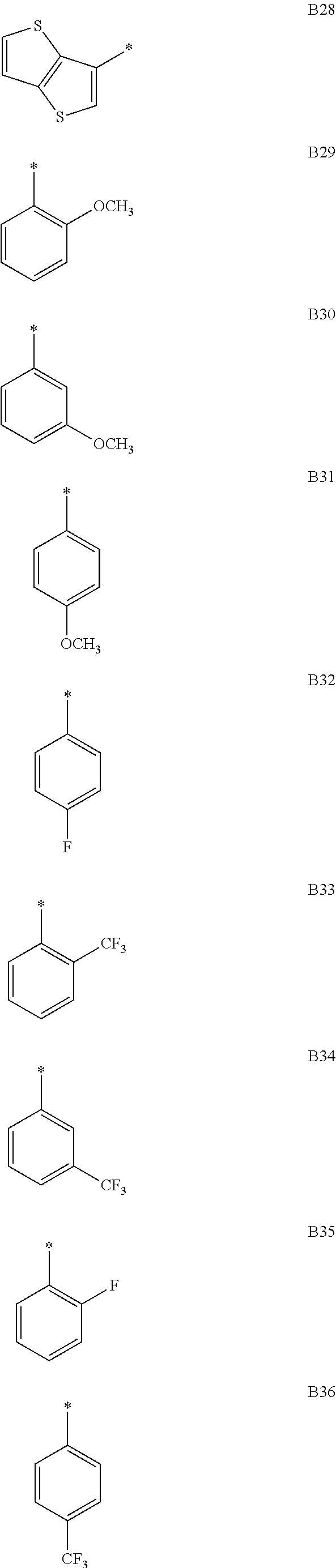
- G1, G2 and G3 can be represented by one of the following formulas B1 through B64, respectively. As such, G1, G2 and G3 are the same as or different from one another.
- the host material has a chemical structure in which indolofluorene becomes an essential ingredient.
- nitrogen N of indolofluorene is chemically and directly bonded with silicon of the substitution group.
- the host material of the present embodiment can have a triplet energy level higher than that of the related art host material such as a CBP material. Therefore, the host material according to an embodiment of the present disclosure can become easier to transfer energy to the dopant, compared to the related art host material.
- the host material has a chemical structure which includes carbazole with a hole-donating property and a silyl group with an electron-donating property, as represented by the formula 1.
- the host material can have bipolarity and maintain the numberical balance between holes and electrons. Therefore, it is not necessary for the host material to add a hole blocking layer and an electron blocking layer.
- the host material has the chemical structure which includes aromatic and silyl groups such as indolofluorene, represented by the formula 1.
- the host material of the present embodiment can have a higher glass transition temperature compared to the related art host material.
- FIG. 1 is a cross-sectional view showing an organic light emitting display device according to a second embodiment of the present disclosure.
- the organic light emitting display device 100 can include an anode 120 , a light emission layer 150 and a cathode 180 which are sequentially disposed on a substrate 110 .
- a material used to form the substrate 110 can be one of glass and a resin. If the substrate 110 is formed from a resin, the resin can become a material which has a lower rate of moisture or oxygen intrusion into the light emission layer 150 compared to the other materials.
- the resin polycarbonate, polyimide, polyethylene terephthalate, polyethylene naphthalate and so on can be used.
- the substrate can be rigid or flexible.
- the anode 120 is directly disposed on the substrate 110 .
- the anode 120 can be formed from a transparent conductive material.
- the anode 120 can be from one of indium-tin-oxide ITO and indium-zinc-oxide IZO.
- the light emission layer 150 is disposed on the anode 120 . Also, the light emission layer 150 can be from a material emitting either green light or blue light.
- the light emission layer 150 can include a blue phosphorescent host material doped with a blue phosphorescent dopant.
- a blue phosphorescent dopant an organometallic complex including one of iridium Ir, platinum Pt and europium Eu can be used.
- the present embodiment is not limited to the above-mentioned blue phosphorescent dopant material.
- Such a blue phosphorescent host material can be represented by the following formula 1.
- the blue phosphorescent host material represented by the formula 1 can become one of compounds being represented by the above-mentioned formulas A1 through A10.
- G1, G2 and G3 can each become one of hydrogen, and aromatic, heterocyclic and aliphatic groups which are or not substituted.
- G1, G2 and G3 can be either the same compound or different compounds from one another.
- a substitute capable of being substituted into the aromatic or heterocyclic compound can include at least one among an alkyl group, an alkoxy group, a halogen group, a silyl group, a cyano group, deuterium, tritium and hydrogen.
- the heterocyclic group can include 4 through 16 carbon atoms C and at least one of one through three nitrogen atoms N, one or two oxygen atoms O and one or two sulfide atoms S.
- G1, G2 and G3 can be represented by one of the above-mentioned formulas B1 through B64, respectively. As such, G1, G2 and G3 are the same as or different from one another.
- the light emission layer 150 when the light emission layer 150 emits green light, the light emission layer 150 can include a green phosphorescent host material doped with a green phosphorescent dopant.
- the green phosphorescent dopant can be an organometallic complex including one of iridium Ir, platinum Pt and europium Eu.
- the present embodiment is not limited to this green phosphorescent dopant material.
- the green phosphorescent host material can be represented by the above-mentioned formula 1.
- the blue and green phosphorescent materials can be represented by the above-mentioned formula 1.
- the blue and green phosphorescent materials can be formed from the same compound or different compounds from each other.
- the light emission layer 150 is one of the blue and green light emission layers
- the light emission layer 150 according to the present embodiment can include red, green and blue light emission layers separated from one another.
- the red, green and blue light emission layers are used to form a single pixel, so that display a variety of colors can be displayed.
- the red light emission layer can include a red phosphorescent host material, such as “4,4′-N,N′-dicarbazole-biphenyl; CBP”, doped with a red phosphorescent dopant such as bis(2-phenylquinoline)(acetylacetonate)iridium; Ir(Phq)2(acac)).
- a red phosphorescent host material such as “4,4′-N,N′-dicarbazole-biphenyl; CBP”
- a red phosphorescent dopant such as bis(2-phenylquinoline)(acetylacetonate)iridium; Ir(Phq)2(acac)
- an embodiment of the present disclosure is not limited to this red light emission layer material.
- the cathode 180 is disposed on the light emission layer 150 .
- the cathode 180 can be formed from a reflective conductive material.
- the cathode 180 can be from one of aluminum Al, silver Ag, chromium Cr, gold Au, tungsten W, titanium Ti and alloys thereof.
- an embodiment of the present embodiment is not limited to these cathode materials.
- the organic light emitting display device 100 can include at least one of a hole injection layer 130 and a hole transport layer 140 which are interposed between the anode 120 and the light emission layer 150 .
- the hole injection layer 130 can be disposed on the anode 120 . Also, the hole injection layer 130 can induce the holes to be emitted from the anode 120 .
- a hole injection layer 130 can be formed from “4,4′-bis[4- ⁇ N,N-bis(3-methylphenyl)amino ⁇ phenyl ⁇ -N-phenylamino]biphenyl; DNTPD”, as an example.
- the hole injection layer 130 is not limited to this material.
- the hole injection layer 130 can be formed from one of “4,4′,4′′-tris(3-methylphenyl-N-phenylamino)triphenylamine; m-MTDATA”, “copper phthalocyanine; Cupc” and so on.
- the hole injection layer 130 can be formed using a vapor deposition method.
- the hole transport layer 140 is used to smoothly transport the holes from the anode 120 to the light emission layer 150 .
- the hole transport layer 140 can prevent electron leakage from the light emission layer 150 .
- Such a hole transport layer 140 can be formed from “N,N′-bis(naphthalene-1-yl)phenyl-N,N-bis(phenyl)-benzidine; NPB”, as an example.
- the hole injection layer 130 and the hole transport layer 140 are included the organic light emitting display device 100 .
- the hole injection layer 130 and the hole transport layer 140 can be sequentially stacked on the anode 120 .
- the organic light emitting display device 100 can further include at one of an electron transport layer 160 and an electron injection layer 170 which are interposed between the light emission layer 150 and the cathode 180 .
- the electron transport layer 160 is used to smoothly transport the electrons emitted from the cathode 180 to the light emission layer 150 . As such, the electron transport layer 160 can prevent hole leakage from the light emission layer 150 to the cathode 180 .
- Such an electron transport layer 160 can be formed from one of “tris-8-hydroxyquinolinato aluminum; Alq3”, “2-(4-biphenyl)-5-(4-tert-butylphenyl)-1,3,4-oxadiazole; PBD” and so on.
- the electron injection layer 170 can induce the electrons to be emitted from the cathode 180 .
- the electron injection layer 170 can be formed from lithium fluoride.
- the organic light emitting display device 100 includes at least one of the hole and electron injection layers 130 and 170 and the hole and electron transport layers 140 and 160 , as well as the light emission layer 150 . In accordance therewith, the luminous efficiency and the life span of the organic light emitting display device 100 can be enhanced.
- the blue phosphorescent compound can be doped into at least one of the hole and electron injection layers 130 and 170 , the light emission layer 150 and the hole and electron transport layers 140 and 160 .
- the organic light emitting display device 100 can enables electric charges to smoothly move.
- the organic light emitting display device 100 can include a sealing member configured to seal the anode 120 , the light emission layer 150 and the cathode 180 .
- the sealing member can shield the anode 120 , the light emission layer 150 and the cathode 180 from the exterior. This results from the fact that the light emission layer 150 is easily deteriorated by external moisture or oxygen.
- Such a sealing member can become an upper substrate which is combined with the above-mentioned substrate 110 in such a manner as to face the substrate 110 with having the anode 120 , the light emission layer 150 and the cathode 180 therebetween.
- the sealing member can become an inorganic insulation film formed to cover the substrate 110 provided with the anode 120 , the light emission layer 150 and the cathode 180 .
- the organic light emitting display device includes a new host material having a triplet energy level higher than that of the related art host material. Therefore, the luminous efficiency of the organic light emitting display device can be enhanced.
- the new host material can have bipolarity. As such, the leakage of holes and/or electrons from the light emission layer 150 can be prevented. Therefore, it is not necessary for the organic light emitting display device to add a hole blocking layer and/or an electron blocking layer.
- the new host material can have a higher glass transition temperature compared to the related art host material. As such, the deformation of the new host material due to heat at a high temperature or a driving temperature can be prevented.
- the organic light emitting display device can have a greatly lengthened life span compared to that of the related art.
- reaction equation 1 The mechanism for the synthesis of indolo(3,2-b)carbazole can be represented by the following reaction equation 1.
- indolo(3,2-b)carbazole synthesized through the experimental example 1 is dissolved in about 100 ml of tetrahydrofuran THF within a 2-neck flask. Also, 17.20 mmol of 2.5M n-butyllithium (n-BuLi) is slowly added little by little into the solution in which indolo(3,2-b)carbazole is dissolved.
- the mechanism for the synthesis of the host material PBH1 can be represented by the following reaction equation 2.
- Table 1 and FIGS. 2 and 3 illustrate test resultants regarding the host material which is obtained through the experimental example 2.
- FIG. 2 is a graphic diagram illustrating UV and PL spectra of a host material according to an embodiment of the present disclosure.
- FIG. 3 is a graphic diagram illustrating low-temperature and normal-temperature PL spectra of a host material according to an embodiment of the present disclosure. In FIG. 3 , the low temperature is set to be 77K.
- the host material obtained through the experimental example 2 has a triplet energy level of 2.76 eV.
- the host material obtained through the experiment example 2 has a higher triplet energy level compared to the related art host material, such as CBP, with the triplet energy level of 2.6 eV.
Landscapes
- Chemical & Material Sciences (AREA)
- Engineering & Computer Science (AREA)
- Materials Engineering (AREA)
- Physics & Mathematics (AREA)
- Organic Chemistry (AREA)
- Spectroscopy & Molecular Physics (AREA)
- Optics & Photonics (AREA)
- Electroluminescent Light Sources (AREA)
Abstract

Wherein the “a” is one selected from a material group which includes N, S, O, SO2 and NSiG1G2G3, and the “G1, G2 and G3” each become one of a hydrogen, and aromatic, heterocyclic and aliphatic groups which are or not substituted, respectively.
Description

Wherein the “a” is one selected from a material group which includes N, S, O, SO2 and NSiG1G2G3, and the “G1, G2 and G3” each become one of a hydrogen, and aromatic, heterocyclic and aliphatic groups which are or not substituted, respectively.

Wherein the “a” is one selected from a material group which includes N, S, O, SO2 and NSiG1G2G3, and the “G1, G2 and G3” each become one of a hydrogen, and aromatic, heterocyclic and aliphatic groups which are or not substituted, respectively.


| TABLE 1 | ||||
| Items | Wavelength(nm) | Energy(eV) | ||
| Excitation Wavelength | 344 | |||
| Energy Bandgap(S1) | 380 | 3.26 | ||
| Triplet Energy(T1) | 450 | 2.76 | ||
Claims (10)


Applications Claiming Priority (2)
| Application Number | Priority Date | Filing Date | Title |
|---|---|---|---|
| KR20110129902A KR20130063405A (en) | 2011-12-06 | 2011-12-06 | Host material and organic light emitting diode device using the same |
| KR10-2011-0129902 | 2011-12-06 |
Publications (2)
| Publication Number | Publication Date |
|---|---|
| US20130140539A1 US20130140539A1 (en) | 2013-06-06 |
| US9123900B2 true US9123900B2 (en) | 2015-09-01 |
Family
ID=48523355
Family Applications (1)
| Application Number | Title | Priority Date | Filing Date |
|---|---|---|---|
| US13/688,479 Active 2033-11-14 US9123900B2 (en) | 2011-12-06 | 2012-11-29 | Host material and organic light emitting display device using the same |
Country Status (2)
| Country | Link |
|---|---|
| US (1) | US9123900B2 (en) |
| KR (1) | KR20130063405A (en) |
Citations (1)
| Publication number | Priority date | Publication date | Assignee | Title |
|---|---|---|---|---|
| JP2001278889A (en) | 2000-03-28 | 2001-10-10 | Fuji Photo Film Co Ltd | New silicon compound, organic luminescent element material and organic luminescent element using the same |
-
2011
- 2011-12-06 KR KR20110129902A patent/KR20130063405A/en not_active Ceased
-
2012
- 2012-11-29 US US13/688,479 patent/US9123900B2/en active Active
Patent Citations (1)
| Publication number | Priority date | Publication date | Assignee | Title |
|---|---|---|---|---|
| JP2001278889A (en) | 2000-03-28 | 2001-10-10 | Fuji Photo Film Co Ltd | New silicon compound, organic luminescent element material and organic luminescent element using the same |
Non-Patent Citations (1)
| Title |
|---|
| Office Action issued in counterpart Korean Patent Application No. 10-2011-0129902 dated Aug. 31, 2014. |
Also Published As
| Publication number | Publication date |
|---|---|
| US20130140539A1 (en) | 2013-06-06 |
| KR20130063405A (en) | 2013-06-14 |
Similar Documents
| Publication | Publication Date | Title |
|---|---|---|
| US10454038B2 (en) | Delayed-fluorescence material and organic electroluminescence element using same | |
| US8906521B2 (en) | Organic electroluminescent device having triptycene derivative material | |
| US9660198B2 (en) | Organic electroluminescence element and compound used therein | |
| US9324958B2 (en) | Red phosphorescent composition and organic electroluminescent device using the same | |
| US11239435B2 (en) | Iridium complex and organic electroluminescence device using the same | |
| US20160020409A1 (en) | Charge transport material, host material, thin film and organic light emitting element | |
| US20100141124A1 (en) | Blue fluorescent compound and organic electroluminescent device using the same | |
| US11236075B2 (en) | Organic compound and organic electroluminescence device using the same | |
| KR20130110934A (en) | Organometallic compounds and organic light emitting diodes comprising the compounds | |
| US20220231231A1 (en) | Organic electroluminescent element, organic electroluminescent display device, and electronic device | |
| US10153438B2 (en) | Organic light-emitting device | |
| US20250127052A1 (en) | Boron compound and organic light-emitting device including same | |
| JP6626047B2 (en) | Boron-containing compound, light emitting layer of organic light emitting diode and organic light emitting diode device | |
| US10224489B2 (en) | Compound and organic electronic device using the same | |
| KR20150124911A (en) | Novel compound and organic electroluminescent device comprising same | |
| TW202231625A (en) | Organic electronic device comprising a compound of formula (i), display device comprising the organic electronic device as well as compounds of formula (i) for use in organic electronic devices | |
| KR101555155B1 (en) | Novel spyrobifluorene type organic compounds and an organic electroluminescent device comprising the same | |
| US7261952B2 (en) | Red color emitting compounds for organic electroluminescent device and an organic electroluminescent device using them | |
| KR20150058083A (en) | Novel electroluminescent compound and organic electroluminescent device comprising same | |
| KR20150064682A (en) | Novel electroluminescent compound and organic electroluminescent device comprising same | |
| JP2006273737A (en) | Aminostyryl compound, organic electroluminescent element, and display device | |
| TWI538560B (en) | Organic electroluminescence element | |
| US20070212569A1 (en) | Organometallic complex for organic light-emitting layer and organic light-emitting diode using the same | |
| US9178164B2 (en) | Organic compound and organic electroluminescent device employing the same | |
| JP4690244B2 (en) | Fluorene compound having tetra-phenylsilane skeleton, light emitting layer host material, hole block material and organic EL device using the same |
Legal Events
| Date | Code | Title | Description |
|---|---|---|---|
| AS | Assignment |
Owner name: LG DISPLAY CO., LTD., KOREA, REPUBLIC OF Free format text: ASSIGNMENT OF ASSIGNORS INTEREST;ASSIGNORS:BIN, JONG KWAN;SONG, IN BUM;KIM, JUNG KEUN;AND OTHERS;REEL/FRAME:029374/0667 Effective date: 20121120 |
|
| FEPP | Fee payment procedure |
Free format text: PAYOR NUMBER ASSIGNED (ORIGINAL EVENT CODE: ASPN); ENTITY STATUS OF PATENT OWNER: LARGE ENTITY |
|
| STCF | Information on status: patent grant |
Free format text: PATENTED CASE |
|
| MAFP | Maintenance fee payment |
Free format text: PAYMENT OF MAINTENANCE FEE, 4TH YEAR, LARGE ENTITY (ORIGINAL EVENT CODE: M1551); ENTITY STATUS OF PATENT OWNER: LARGE ENTITY Year of fee payment: 4 |
|
| MAFP | Maintenance fee payment |
Free format text: PAYMENT OF MAINTENANCE FEE, 8TH YEAR, LARGE ENTITY (ORIGINAL EVENT CODE: M1552); ENTITY STATUS OF PATENT OWNER: LARGE ENTITY Year of fee payment: 8 |