US9123789B2 - Chip with through silicon via electrode and method of forming the same - Google Patents
Chip with through silicon via electrode and method of forming the same Download PDFInfo
- Publication number
- US9123789B2 US9123789B2 US13/747,492 US201313747492A US9123789B2 US 9123789 B2 US9123789 B2 US 9123789B2 US 201313747492 A US201313747492 A US 201313747492A US 9123789 B2 US9123789 B2 US 9123789B2
- Authority
- US
- United States
- Prior art keywords
- substrate
- layer
- conductive layer
- chip
- disposed
- Prior art date
- Legal status (The legal status is an assumption and is not a legal conclusion. Google has not performed a legal analysis and makes no representation as to the accuracy of the status listed.)
- Active
Links
Images


Classifications
-
- H01L21/76898—
-
- H—ELECTRICITY
- H10—SEMICONDUCTOR DEVICES; ELECTRIC SOLID-STATE DEVICES NOT OTHERWISE PROVIDED FOR
- H10W—GENERIC PACKAGES, INTERCONNECTIONS, CONNECTORS OR OTHER CONSTRUCTIONAL DETAILS OF DEVICES COVERED BY CLASS H10
- H10W20/00—Interconnections in chips, wafers or substrates
- H10W20/01—Manufacture or treatment
- H10W20/021—Manufacture or treatment of interconnections within wafers or substrates
- H10W20/023—Manufacture or treatment of interconnections within wafers or substrates the interconnections being through-semiconductor vias
-
- H01L23/481—
-
- H01L23/49827—
-
- H01L23/5226—
-
- H01L24/16—
-
- H—ELECTRICITY
- H10—SEMICONDUCTOR DEVICES; ELECTRIC SOLID-STATE DEVICES NOT OTHERWISE PROVIDED FOR
- H10P—GENERIC PROCESSES OR APPARATUS FOR THE MANUFACTURE OR TREATMENT OF DEVICES COVERED BY CLASS H10
- H10P14/00—Formation of materials, e.g. in the shape of layers or pillars
- H10P14/40—Formation of materials, e.g. in the shape of layers or pillars of conductive or resistive materials
-
- H—ELECTRICITY
- H10—SEMICONDUCTOR DEVICES; ELECTRIC SOLID-STATE DEVICES NOT OTHERWISE PROVIDED FOR
- H10P—GENERIC PROCESSES OR APPARATUS FOR THE MANUFACTURE OR TREATMENT OF DEVICES COVERED BY CLASS H10
- H10P50/00—Etching of wafers, substrates or parts of devices
-
- H—ELECTRICITY
- H10—SEMICONDUCTOR DEVICES; ELECTRIC SOLID-STATE DEVICES NOT OTHERWISE PROVIDED FOR
- H10W—GENERIC PACKAGES, INTERCONNECTIONS, CONNECTORS OR OTHER CONSTRUCTIONAL DETAILS OF DEVICES COVERED BY CLASS H10
- H10W20/00—Interconnections in chips, wafers or substrates
- H10W20/01—Manufacture or treatment
- H10W20/021—Manufacture or treatment of interconnections within wafers or substrates
- H10W20/023—Manufacture or treatment of interconnections within wafers or substrates the interconnections being through-semiconductor vias
- H10W20/0234—Manufacture or treatment of interconnections within wafers or substrates the interconnections being through-semiconductor vias comprising etching via holes that stop on pads or on electrodes
-
- H—ELECTRICITY
- H10—SEMICONDUCTOR DEVICES; ELECTRIC SOLID-STATE DEVICES NOT OTHERWISE PROVIDED FOR
- H10W—GENERIC PACKAGES, INTERCONNECTIONS, CONNECTORS OR OTHER CONSTRUCTIONAL DETAILS OF DEVICES COVERED BY CLASS H10
- H10W20/00—Interconnections in chips, wafers or substrates
- H10W20/01—Manufacture or treatment
- H10W20/021—Manufacture or treatment of interconnections within wafers or substrates
- H10W20/023—Manufacture or treatment of interconnections within wafers or substrates the interconnections being through-semiconductor vias
- H10W20/0242—Manufacture or treatment of interconnections within wafers or substrates the interconnections being through-semiconductor vias comprising etching via holes from the back sides of the chips, wafers or substrates
-
- H—ELECTRICITY
- H10—SEMICONDUCTOR DEVICES; ELECTRIC SOLID-STATE DEVICES NOT OTHERWISE PROVIDED FOR
- H10W—GENERIC PACKAGES, INTERCONNECTIONS, CONNECTORS OR OTHER CONSTRUCTIONAL DETAILS OF DEVICES COVERED BY CLASS H10
- H10W20/00—Interconnections in chips, wafers or substrates
- H10W20/01—Manufacture or treatment
- H10W20/021—Manufacture or treatment of interconnections within wafers or substrates
- H10W20/023—Manufacture or treatment of interconnections within wafers or substrates the interconnections being through-semiconductor vias
- H10W20/0245—Manufacture or treatment of interconnections within wafers or substrates the interconnections being through-semiconductor vias comprising use of blind vias during the manufacture
-
- H—ELECTRICITY
- H10—SEMICONDUCTOR DEVICES; ELECTRIC SOLID-STATE DEVICES NOT OTHERWISE PROVIDED FOR
- H10W—GENERIC PACKAGES, INTERCONNECTIONS, CONNECTORS OR OTHER CONSTRUCTIONAL DETAILS OF DEVICES COVERED BY CLASS H10
- H10W20/00—Interconnections in chips, wafers or substrates
- H10W20/01—Manufacture or treatment
- H10W20/021—Manufacture or treatment of interconnections within wafers or substrates
- H10W20/023—Manufacture or treatment of interconnections within wafers or substrates the interconnections being through-semiconductor vias
- H10W20/0257—Manufacture or treatment of interconnections within wafers or substrates the interconnections being through-semiconductor vias comprising using a sacrificial placeholder, e.g. using a sacrificial plug
-
- H—ELECTRICITY
- H10—SEMICONDUCTOR DEVICES; ELECTRIC SOLID-STATE DEVICES NOT OTHERWISE PROVIDED FOR
- H10W—GENERIC PACKAGES, INTERCONNECTIONS, CONNECTORS OR OTHER CONSTRUCTIONAL DETAILS OF DEVICES COVERED BY CLASS H10
- H10W20/00—Interconnections in chips, wafers or substrates
- H10W20/01—Manufacture or treatment
- H10W20/031—Manufacture or treatment of conductive parts of the interconnections
- H10W20/032—Manufacture or treatment of conductive parts of the interconnections of conductive barrier, adhesion or liner layers
- H10W20/038—Manufacture or treatment of conductive parts of the interconnections of conductive barrier, adhesion or liner layers covering conductive structures
-
- H—ELECTRICITY
- H10—SEMICONDUCTOR DEVICES; ELECTRIC SOLID-STATE DEVICES NOT OTHERWISE PROVIDED FOR
- H10W—GENERIC PACKAGES, INTERCONNECTIONS, CONNECTORS OR OTHER CONSTRUCTIONAL DETAILS OF DEVICES COVERED BY CLASS H10
- H10W20/00—Interconnections in chips, wafers or substrates
- H10W20/01—Manufacture or treatment
- H10W20/031—Manufacture or treatment of conductive parts of the interconnections
- H10W20/032—Manufacture or treatment of conductive parts of the interconnections of conductive barrier, adhesion or liner layers
- H10W20/042—Manufacture or treatment of conductive parts of the interconnections of conductive barrier, adhesion or liner layers the barrier, adhesion or liner layers being seed or nucleation layers
-
- H—ELECTRICITY
- H10—SEMICONDUCTOR DEVICES; ELECTRIC SOLID-STATE DEVICES NOT OTHERWISE PROVIDED FOR
- H10W—GENERIC PACKAGES, INTERCONNECTIONS, CONNECTORS OR OTHER CONSTRUCTIONAL DETAILS OF DEVICES COVERED BY CLASS H10
- H10W20/00—Interconnections in chips, wafers or substrates
- H10W20/01—Manufacture or treatment
- H10W20/031—Manufacture or treatment of conductive parts of the interconnections
- H10W20/032—Manufacture or treatment of conductive parts of the interconnections of conductive barrier, adhesion or liner layers
- H10W20/054—Manufacture or treatment of conductive parts of the interconnections of conductive barrier, adhesion or liner layers by selectively removing parts thereof
-
- H—ELECTRICITY
- H10—SEMICONDUCTOR DEVICES; ELECTRIC SOLID-STATE DEVICES NOT OTHERWISE PROVIDED FOR
- H10W—GENERIC PACKAGES, INTERCONNECTIONS, CONNECTORS OR OTHER CONSTRUCTIONAL DETAILS OF DEVICES COVERED BY CLASS H10
- H10W20/00—Interconnections in chips, wafers or substrates
- H10W20/01—Manufacture or treatment
- H10W20/031—Manufacture or treatment of conductive parts of the interconnections
- H10W20/056—Manufacture or treatment of conductive parts of the interconnections by filling conductive material into holes, grooves or trenches
-
- H—ELECTRICITY
- H10—SEMICONDUCTOR DEVICES; ELECTRIC SOLID-STATE DEVICES NOT OTHERWISE PROVIDED FOR
- H10W—GENERIC PACKAGES, INTERCONNECTIONS, CONNECTORS OR OTHER CONSTRUCTIONAL DETAILS OF DEVICES COVERED BY CLASS H10
- H10W20/00—Interconnections in chips, wafers or substrates
- H10W20/20—Interconnections within wafers or substrates, e.g. through-silicon vias [TSV]
-
- H—ELECTRICITY
- H10—SEMICONDUCTOR DEVICES; ELECTRIC SOLID-STATE DEVICES NOT OTHERWISE PROVIDED FOR
- H10W—GENERIC PACKAGES, INTERCONNECTIONS, CONNECTORS OR OTHER CONSTRUCTIONAL DETAILS OF DEVICES COVERED BY CLASS H10
- H10W20/00—Interconnections in chips, wafers or substrates
- H10W20/40—Interconnections external to wafers or substrates, e.g. back-end-of-line [BEOL] metallisations or vias connecting to gate electrodes
- H10W20/41—Interconnections external to wafers or substrates, e.g. back-end-of-line [BEOL] metallisations or vias connecting to gate electrodes characterised by their conductive parts
- H10W20/42—Vias, e.g. via plugs
-
- H—ELECTRICITY
- H10—SEMICONDUCTOR DEVICES; ELECTRIC SOLID-STATE DEVICES NOT OTHERWISE PROVIDED FOR
- H10W—GENERIC PACKAGES, INTERCONNECTIONS, CONNECTORS OR OTHER CONSTRUCTIONAL DETAILS OF DEVICES COVERED BY CLASS H10
- H10W70/00—Package substrates; Interposers; Redistribution layers [RDL]
- H10W70/60—Insulating or insulated package substrates; Interposers; Redistribution layers
- H10W70/62—Insulating or insulated package substrates; Interposers; Redistribution layers characterised by their interconnections
- H10W70/63—Vias, e.g. via plugs
- H10W70/635—Through-vias
-
- H—ELECTRICITY
- H10—SEMICONDUCTOR DEVICES; ELECTRIC SOLID-STATE DEVICES NOT OTHERWISE PROVIDED FOR
- H10W—GENERIC PACKAGES, INTERCONNECTIONS, CONNECTORS OR OTHER CONSTRUCTIONAL DETAILS OF DEVICES COVERED BY CLASS H10
- H10W72/00—Interconnections or connectors in packages
- H10W72/01—Manufacture or treatment
- H10W72/019—Manufacture or treatment of bond pads
-
- H—ELECTRICITY
- H10—SEMICONDUCTOR DEVICES; ELECTRIC SOLID-STATE DEVICES NOT OTHERWISE PROVIDED FOR
- H10W—GENERIC PACKAGES, INTERCONNECTIONS, CONNECTORS OR OTHER CONSTRUCTIONAL DETAILS OF DEVICES COVERED BY CLASS H10
- H10W72/00—Interconnections or connectors in packages
- H10W72/20—Bump connectors, e.g. solder bumps or copper pillars; Dummy bumps; Thermal bumps
-
- H01L2224/4824—
-
- H01L2225/06513—
-
- H01L2225/06541—
-
- H01L28/60—
-
- H01L2924/00—
-
- H01L2924/0002—
-
- H—ELECTRICITY
- H10—SEMICONDUCTOR DEVICES; ELECTRIC SOLID-STATE DEVICES NOT OTHERWISE PROVIDED FOR
- H10D—INORGANIC ELECTRIC SEMICONDUCTOR DEVICES
- H10D1/00—Resistors, capacitors or inductors
- H10D1/60—Capacitors
- H10D1/68—Capacitors having no potential barriers
- H10D1/692—Electrodes
-
- H—ELECTRICITY
- H10—SEMICONDUCTOR DEVICES; ELECTRIC SOLID-STATE DEVICES NOT OTHERWISE PROVIDED FOR
- H10W—GENERIC PACKAGES, INTERCONNECTIONS, CONNECTORS OR OTHER CONSTRUCTIONAL DETAILS OF DEVICES COVERED BY CLASS H10
- H10W70/00—Package substrates; Interposers; Redistribution layers [RDL]
- H10W70/01—Manufacture or treatment
- H10W70/05—Manufacture or treatment of insulating or insulated package substrates, or of interposers, or of redistribution layers
-
- H—ELECTRICITY
- H10—SEMICONDUCTOR DEVICES; ELECTRIC SOLID-STATE DEVICES NOT OTHERWISE PROVIDED FOR
- H10W—GENERIC PACKAGES, INTERCONNECTIONS, CONNECTORS OR OTHER CONSTRUCTIONAL DETAILS OF DEVICES COVERED BY CLASS H10
- H10W72/00—Interconnections or connectors in packages
- H10W72/20—Bump connectors, e.g. solder bumps or copper pillars; Dummy bumps; Thermal bumps
- H10W72/29—Bond pads specially adapted therefor
-
- H—ELECTRICITY
- H10—SEMICONDUCTOR DEVICES; ELECTRIC SOLID-STATE DEVICES NOT OTHERWISE PROVIDED FOR
- H10W—GENERIC PACKAGES, INTERCONNECTIONS, CONNECTORS OR OTHER CONSTRUCTIONAL DETAILS OF DEVICES COVERED BY CLASS H10
- H10W90/00—Package configurations
- H10W90/20—Configurations of stacked chips
- H10W90/297—Configurations of stacked chips characterised by the through-semiconductor vias [TSVs] in the stacked chips
-
- H—ELECTRICITY
- H10—SEMICONDUCTOR DEVICES; ELECTRIC SOLID-STATE DEVICES NOT OTHERWISE PROVIDED FOR
- H10W—GENERIC PACKAGES, INTERCONNECTIONS, CONNECTORS OR OTHER CONSTRUCTIONAL DETAILS OF DEVICES COVERED BY CLASS H10
- H10W90/00—Package configurations
- H10W90/701—Package configurations characterised by the relative positions of pads or connectors relative to package parts
- H10W90/721—Package configurations characterised by the relative positions of pads or connectors relative to package parts of bump connectors
- H10W90/722—Package configurations characterised by the relative positions of pads or connectors relative to package parts of bump connectors between stacked chips
-
- H—ELECTRICITY
- H10—SEMICONDUCTOR DEVICES; ELECTRIC SOLID-STATE DEVICES NOT OTHERWISE PROVIDED FOR
- H10W—GENERIC PACKAGES, INTERCONNECTIONS, CONNECTORS OR OTHER CONSTRUCTIONAL DETAILS OF DEVICES COVERED BY CLASS H10
- H10W90/00—Package configurations
- H10W90/701—Package configurations characterised by the relative positions of pads or connectors relative to package parts
- H10W90/751—Package configurations characterised by the relative positions of pads or connectors relative to package parts of bond wires
- H10W90/754—Package configurations characterised by the relative positions of pads or connectors relative to package parts of bond wires between a chip and a stacked insulating package substrate, interposer or RDL
Definitions
- the present invention relates to a chip and the forming method thereof, and more particularly, to a chip with a through silicon via (TSV) electrode and the forming method thereof.
- TSV through silicon via
- IC integrated circuits
- an IC device is produced from dies that are fabricated by conventional semiconductor manufacturing processes.
- the process to manufacture a die starts with a wafer: first, different regions are marked on the wafer; second, conventional semiconductor manufacture processes such as deposition, photolithography, etching or planarization are used to form needed circuit trace(s); then, each region of the wafer is separated to form a die and packaged to form a chip; finally, the chip is attached onto a board, for example, a printed circuit board (PCB), and the chip is electrically coupled to the pins on the PCB.
- PCB printed circuit board
- TSV Through Silicon Via
- the present invention therefore provides a chip with TSV electrode and a method of forming the same, which can save the cost of the processes.
- a method of forming a chip with TSV electrode is provided.
- a substrate with a first surface and a second surface is provided.
- a thinning process is performed from a side of the second surface so the second surface becomes a third surface.
- a penetration via which penetrates through the first surface and the third surface is formed in the substrate.
- a patterned material layer is formed on the substrate, wherein the patterned material layer has an opening exposes the penetration via.
- a conductive layer is formed on the third surface thereby simultaneously forming a TSV electrode in the penetration via and a surface conductive layer in the opening.
- a chip with a TSV electrode includes a substrate, a penetration via, a TSV electrode and a surface conductive layer.
- the substrate includes a first surface and a third surface.
- the penetration via is disposed in the substrate and penetrates through the first surface and the third surface.
- the TSV electrode is disposed in the penetration via.
- the surface conductive layer is disposed on the third surface outside the penetration via and is monolithic with the TSV electrode.
- the TSV electrode and the surface conductive layer are monolithic, thereby saving the manufacturing cost.
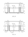
- FIG. 1 to FIG. 7 show schematic diagrams of the method of forming a chip with a TSV electrode according to the first embodiment of the present invention.
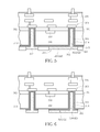
- FIG. 8 to FIG. 10 show schematic diagrams of the method of forming a chip with a TSV electrode according to the second embodiment of the present invention.
- a substrate 300 is provided, such as a silicon substrate, an epitaxial silicon substrate, a silicon germanium substrate, a silicon carbide substrate or a silicon-on-insulator substrate (SOI), but is not limited thereto.
- the substrate 300 has a first surface 302 and a second surface 304 , which are opposite to each other.
- the first surface 302 is the active surface of the substrate 300 and the second surface 304 is the back surface of the substrate 300 .
- a thickness of the substrate 300 is about 700 to 1000 micro meters.
- a semiconductor device 303 such as a metal oxide semiconductor transistor (MOS transistor) or a memory cell of a dynamic random access memory (DRAM) is formed on the first surface 302 of the substrate 300 .
- An inter-dielectric layer (ILD) 301 such as a SiO 2 layer is formed on a side of the first surface 302 to cover the semiconductor device 303 .
- a plurality of intra-metal dielectric layers (IMD layer) 306 and a metal interconnection system 308 in the IMD layers 306 are formed on the ILD layer 301 .
- the metal interconnection system 308 may be electrically connected to the semiconductor device 303 by a contact plug so the semiconductor device 303 can receive or send out signals.
- a thinning process is carried out from the second surface 304 of the substrate 300 to thin the substrate 300 to a determined thickness, such as 10 to 100 micro meters.
- the second surface 304 therefore becomes a third surface 310 .
- a penetration via 312 is formed from a side of the third surface 310 of the substrate 300 wherein the penetration via 312 penetrates through the first surface 302 and the third surface 310 , preferably through the ILD layer 301 so as to expose a part of the metal interconnection system 308 .
- the process of forming the penetration via 312 can be a dry etching process.
- an aperture of the penetration via 312 is about 5 to 100 micro meters, but is not limited thereto. It is understood that the type or the forming method of the penetration via 312 can be adjusted according to different designs of the products.
- a dielectric layer 314 is formed on the third surface 310 of the substrate 300 and on the surface of the penetration via 312 .
- the dielectric layer 314 covers the sidewall of the penetration via 312 , but does not covers the bottom surface of the penetration via 312 .
- the dielectric layer 314 is a SiO 2 layer and is formed by a thermal oxidation process which only reacts with the exposed substrate 300 .
- the dielectric layer 314 is not formed on the surface of the metal interconnection system 308 .
- an optional barrier layer 316 and an optional seed layer 315 are sequentially formed on the dielectric layer 314 .
- the barrier layer 316 and the seed layer 315 are formed conformally along the sidewall and the bottom surface of the penetration via 312 and the third surface 310 .
- the method of forming the barrier layer 316 and the seed layer 315 can be, for example, a chemical vapor deposition (CVD) or a physical vapor deposition (PVD).
- the barrier layer 316 is nitride titanium (TiN), titanium (Ti), tantalum nitride (TaN), tantalum (Ta) or combinations thereof
- an the seed layer 315 is a copper seed layer.
- a patterned material layer 320 is formed on the third surface 310 of the substrate 300 and covers the barrier layer 316 and the seed layer 315 .
- the patterned material layer 320 has at least an opening 318 which exposes the penetration via 312 .
- a width of the opening 312 is greater than that of the penetration via 312 so as to define the position of the TSV electrode and the redistribution layer (RDL) in the subsequent steps.
- the patterned material layer 320 is a photoresist layer and is formed through a lithography process.
- the patterning material layer 320 can be a mask layer and is formed by a lithography process and an etching process.
- a conductive layer 322 such as a copper layer is formed in the penetration via 312 in the substrate 300 and in the opening 318 in the patterning material layer 320 .
- the conductive layer 322 can be formed by an electroplating process. Since a part of the seed layer 315 is covered by the patterned material layer 320 , so the conductive layer 322 is formed only on the exposed seed layer 315 .
- the conductive layer 322 located in the penetration via 312 becomes a TSV electrode 324 and the conductive layer 322 located in the opening 318 becomes a surface conductive layer 326 .
- the TSV electrode 324 and the surface conductive layer 326 are formed simultaneously in the same step, the TSV electrode 324 and the surface conductive layer 326 are monolithic and no interface is formed therebetween.
- the surface conductive layer 326 has a fine flat surface, so no additional planarization process is required.
- the patterned material layer 320 is removed.
- the seed layer 315 and the barrier layer 316 below the patterned material layer 320 are further removed to ensure that the TSV electrodes 324 will not short with each other.
- the conductive layer 326 , the seed layer 315 and the barrier layer 316 are vertically aligned.
- the surface conductive layer 326 can be an RDL layer or a part or a whole of an integrated passive device (IPD).
- the integrated passive device can a resistor, a capacitor, an inductor or an antenna.
- the surface conductive layer 326 is an RDL.
- an electrical connection element such as a solder bump can be formed on the surface conductive layer 326 to provide an electrical pathway to another chip or a printed circuit board (PCB).
- the IPD can be of different types.
- one or a plurality of dielectric layers 331 can be formed on the surface conductive layer 326 , following by forming a metal layer 333 on the dielectric layer 331 .
- the metal layer 333 , the dielectric layer 331 and the conductive layer 326 constitute a capacitor structure.
- a bump 328 can be formed to contact the surface metal layer 326 to provide an electrical pathway to another chip or a PCB.
- the present invention provides a chip with a TSV electrode.
- the chip includes a substrate 300 , a penetration via 312 , a TSV electrode 324 and an IPD 335 .
- the substrate 300 has a first surface 302 and a third surface 310 .
- the penetration via 312 is disposed in the substrate 300 and penetrates through the first surface 302 and the third surface 310 .
- the TSV electrode 324 is disposed in the penetration via 312 .
- the IPD 335 is disposed on a side of the third surface 310 of the substrate 300 .
- the IPD 335 includes a surface conductive layer 326 , which is located on the third surface 310 outside the penetration via 312 and is monolithic with the TSV electrode 324 .
- the chip further includes a barrier layer 316 or a seed layer 315 which is disposed between the surface conductive layer 326 , the TSV electrode 324 and the substrate 300 .
- the barrier layer 316 , the seed layer 315 and the surface conductive layer 326 are vertically aligned along third surface 310 . It is noted that, in another embodiment, the barrier layer 316 and/or the seed layer 315 may be omitted depending on the design of the product.
- a substrate 300 is provided, such as a silicon substrate, an epitaxial silicon substrate, a silicon germanium substrate, a silicon carbide substrate or a silicon-on-insulator substrate (SOI), but is not limited thereto.
- the substrate 300 has a first surface 302 and a second surface 304 , which are opposite to each other.
- the first surface 302 is the active surface of the substrate 300 and the second surface 304 is the back surface of the substrate 300 for example.
- a thickness of the substrate 300 is about 700 to 1000 micro meters.
- a via 330 is formed on the first surface 302 of the substrate 300 .
- An aperture of the via 330 is about 5 to 10 micro meters and a depth of the via 330 is about 50 to 100 micro meters, but is not limited thereto.
- a sacrificial layer 332 is formed on the substrate 300 to fill into the via 330 .
- the step of forming the sacrificial layer 332 can include a deposition process and a planarization process such as a chemical mechanical polish (CMP) process.
- the sacrificial layer 332 can include dielectric material, spin-on glass (SOG), or photoresist.
- the sacrificial layer 332 is SOG which can provide good filling capability.
- a semiconductor device 303 such as a MOS transistor or a DRAM memory cell is formed on the first surface 302 of the substrate 300 .
- an ILD 301 such as a SiO 2 layer is formed on a side of the first surface 302 to cover the semiconductor device 303 .
- a plurality of IMD layers 306 and a metal interconnection system 308 in the IMD layers 306 are formed over the ILD layer 301 .
- the metal interconnection system 308 may be electrically connected to the semiconductor device 303 by a contact plug.
- a thinning process is performed from a second surface 304 of the substrate 300 to expose the sacrificial layer 332 .
- the sacrificial layer 332 is then removed.
- the second surface 304 becomes a third surface 310
- the via 330 becomes a penetration via 312 which penetrates through the first surface 302 and the third surface 310 .
- the following steps can be proceeded in accordance with the first embodiment in FIG. 3 , and are not described repeatedly.
- the penetration via 312 in the second embodiment has a different length with respect to the first embodiment. That is, the penetration via 312 in the first embodiment penetrates further to the ILD layer 301 while the penetration via 312 in the second embodiment only penetrates the substrate 300 .
- the present invention provides a chip with a TSV electrode and a method of forming the same.
- the TSV electrode and the surface conductive layer are monolithic. Thus, the manufacturing cost can be saved.
Landscapes
- Internal Circuitry In Semiconductor Integrated Circuit Devices (AREA)
- Engineering & Computer Science (AREA)
- Manufacturing & Machinery (AREA)
- Power Engineering (AREA)
Abstract
Description
Claims (8)
Priority Applications (2)
| Application Number | Priority Date | Filing Date | Title |
|---|---|---|---|
| US13/747,492 US9123789B2 (en) | 2013-01-23 | 2013-01-23 | Chip with through silicon via electrode and method of forming the same |
| US14/791,265 US9437491B2 (en) | 2013-01-23 | 2015-07-03 | Method of forming chip with through silicon via electrode |
Applications Claiming Priority (1)
| Application Number | Priority Date | Filing Date | Title |
|---|---|---|---|
| US13/747,492 US9123789B2 (en) | 2013-01-23 | 2013-01-23 | Chip with through silicon via electrode and method of forming the same |
Related Child Applications (1)
| Application Number | Title | Priority Date | Filing Date |
|---|---|---|---|
| US14/791,265 Division US9437491B2 (en) | 2013-01-23 | 2015-07-03 | Method of forming chip with through silicon via electrode |
Publications (2)
| Publication Number | Publication Date |
|---|---|
| US20140203394A1 US20140203394A1 (en) | 2014-07-24 |
| US9123789B2 true US9123789B2 (en) | 2015-09-01 |
Family
ID=51207079
Family Applications (2)
| Application Number | Title | Priority Date | Filing Date |
|---|---|---|---|
| US13/747,492 Active US9123789B2 (en) | 2013-01-23 | 2013-01-23 | Chip with through silicon via electrode and method of forming the same |
| US14/791,265 Active US9437491B2 (en) | 2013-01-23 | 2015-07-03 | Method of forming chip with through silicon via electrode |
Family Applications After (1)
| Application Number | Title | Priority Date | Filing Date |
|---|---|---|---|
| US14/791,265 Active US9437491B2 (en) | 2013-01-23 | 2015-07-03 | Method of forming chip with through silicon via electrode |
Country Status (1)
| Country | Link |
|---|---|
| US (2) | US9123789B2 (en) |
Cited By (7)
| Publication number | Priority date | Publication date | Assignee | Title |
|---|---|---|---|---|
| US20170221796A1 (en) * | 2016-01-29 | 2017-08-03 | United Microelectronics Corp. | Through-silicon via structure |
| US10103093B2 (en) | 2014-03-12 | 2018-10-16 | Invensas Corporation | Via structure for signal equalization |
| US11239171B2 (en) * | 2019-11-07 | 2022-02-01 | Samsung Electronics Co., Ltd. | Semiconductor device and semiconductor package including the same |
| US11355386B2 (en) * | 2017-09-20 | 2022-06-07 | Ams Ag | Method for manufacturing a semiconductor device and semiconductor device |
| US11587955B2 (en) * | 2019-07-24 | 2023-02-21 | Shenzhen China Star Optoelectronics Semiconductor Display Technology Co., Ltd. | TFT backplane and micro-LED display |
| US20240021537A1 (en) * | 2022-07-14 | 2024-01-18 | Taiwan Semiconductor Manufacturing Co., Ltd. | Low-noise package and method |
| US12205909B2 (en) | 2021-01-26 | 2025-01-21 | United Microelectronics Corp. | Semiconductor device and method for fabricating the same |
Families Citing this family (10)
| Publication number | Priority date | Publication date | Assignee | Title |
|---|---|---|---|---|
| US9129981B2 (en) * | 2013-11-26 | 2015-09-08 | Freescale Semiconductor Inc. | Methods for the production of microelectronic packages having radiofrequency stand-off layers |
| CN105514047A (en) * | 2014-10-13 | 2016-04-20 | 中芯国际集成电路制造(上海)有限公司 | Wafer level packaging method |
| US9502347B2 (en) | 2015-02-23 | 2016-11-22 | Invensas Corporation | Microelectronic assemblies formed using metal silicide, and methods of fabrication |
| KR102357937B1 (en) * | 2015-08-26 | 2022-02-04 | 삼성전자주식회사 | Semiconductor chip, method for fabricating the same, and semiconductor package comprising the same |
| KR102372349B1 (en) | 2015-08-26 | 2022-03-11 | 삼성전자주식회사 | Semiconductor chip, method for fabricating the same, and semiconductor package comprising the same |
| CN112164688B (en) * | 2017-07-21 | 2023-06-13 | 联华电子股份有限公司 | Chip stacking structure and manufacturing method of chip stacking structure |
| KR102504834B1 (en) * | 2019-03-11 | 2023-02-28 | 삼성전자 주식회사 | Integrated circuit chip, method of manufacturing integrated circuit chip, and integrated circuit package and display apparatus including integrated circuit chip |
| US10910345B2 (en) | 2019-05-02 | 2021-02-02 | Nanya Technology Corporation | Semiconductor device with stacked die device |
| US11264340B2 (en) * | 2019-11-26 | 2022-03-01 | Advanced Semiconductor Engineering, Inc. | Semiconductor devices, semiconductor device packages and method for manufacturing the same |
| TWI737523B (en) | 2020-10-26 | 2021-08-21 | 力晶積成電子製造股份有限公司 | Through silicon via and method of manufacturing the same |
Citations (48)
| Publication number | Priority date | Publication date | Assignee | Title |
|---|---|---|---|---|
| US20050133930A1 (en) * | 2003-12-17 | 2005-06-23 | Sergey Savastisuk | Packaging substrates for integrated circuits and soldering methods |
| US20060040423A1 (en) * | 2003-12-17 | 2006-02-23 | Sergey Savastibuk | Attachment of integrated circuit structures and other substrates to substrates with vias |
| US7410884B2 (en) * | 2005-11-21 | 2008-08-12 | Intel Corporation | 3D integrated circuits using thick metal for backside connections and offset bumps |
| US20090294983A1 (en) * | 2008-06-03 | 2009-12-03 | Micron Technology, Inc. | Hybrid conductive vias including small dimension active surface ends and larger dimension back side ends, semiconductor devices including the same, and associated methods |
| US20090315154A1 (en) * | 2008-06-19 | 2009-12-24 | Micron Technology, Inc. | Semiconductor with through-substrate interconnect |
| US20100130003A1 (en) * | 2008-11-25 | 2010-05-27 | Chuan-Yi Lin | Method of Forming Through-Silicon Vias |
| US20100140752A1 (en) * | 2008-12-10 | 2010-06-10 | Stats Chippac, Ltd. | Semiconductor Device and Method of Forming Compliant Polymer Layer Between UBM and Conformal Dielectric Layer/RDL for Stress Relief |
| US20100144118A1 (en) * | 2008-12-08 | 2010-06-10 | Ku-Feng Yang | Method for Stacking Semiconductor Dies |
| US20100178747A1 (en) * | 2009-01-13 | 2010-07-15 | Maxim Integrated Products, Inc. | Minimum Cost Method for Forming High Density Passive Capacitors for Replacement of Discrete Board Capacitors Using a Minimum Cost 3D Wafer-to-Wafer Modular Integration Scheme |
| US20100244208A1 (en) * | 2009-03-25 | 2010-09-30 | Stats Chippac, Ltd. | Semiconductor Device and Method of Forming a Shielding Layer Between Stacked Semiconductor Die |
| US20100252934A1 (en) * | 2009-04-07 | 2010-10-07 | Taiwan Semiconductor Manufacturing Company, Ltd. | Three-Dimensional Semiconductor Architecture |
| US20100264512A1 (en) * | 2008-09-17 | 2010-10-21 | Stats Chippac, Ltd. | Semiconductor Device and Method of Forming High-Frequency Circuit Structure and Method Thereof |
| US20100308443A1 (en) * | 2009-06-08 | 2010-12-09 | Stats Chippac, Ltd. | Semiconductor Device and Method of Forming an Interconnect Structure with TSV Using Encapsulant for Structural Support |
| US20110210452A1 (en) * | 2008-10-30 | 2011-09-01 | Nxp B.V. | Through-substrate via and redistribution layer with metal paste |
| US8039303B2 (en) * | 2008-06-11 | 2011-10-18 | Stats Chippac, Ltd. | Method of forming stress relief layer between die and interconnect structure |
| US20110254165A1 (en) * | 2010-04-19 | 2011-10-20 | Renesas Electronics Corporation | Semiconductor integrated circuit device and production method thereof |
| US20120056331A1 (en) * | 2010-09-06 | 2012-03-08 | Electronics And Telecommunications Research Institute | Methods of forming semiconductor device and semiconductor devices formed by the same |
| US20120056330A1 (en) * | 2010-09-07 | 2012-03-08 | Samsung Electronics Co., Ltd. | Semiconductor device |
| US20120074584A1 (en) * | 2010-09-27 | 2012-03-29 | Samsung Electronics Co., Ltd. | Multi-layer tsv insulation and methods of fabricating the same |
| US20120083116A1 (en) * | 2010-09-30 | 2012-04-05 | Taiwan Semiconductor Manufacturing Company, Ltd. | Cost-Effective TSV Formation |
| US20120091520A1 (en) * | 2010-10-15 | 2012-04-19 | Elpida Memory, Inc. | Semiconductor device, method for forming the same, and data processing system |
| US20120112361A1 (en) * | 2010-11-08 | 2012-05-10 | Han Kyu-Hee | Semiconductor devices and methods of manufacturing the same |
| US20120133048A1 (en) * | 2010-11-29 | 2012-05-31 | Samsung Electronics Co., Ltd. | Semiconductor device, fabricating method thereof and semiconductor package including the semiconductor device |
| US20120142185A1 (en) * | 2010-12-03 | 2012-06-07 | Samsung Electronics Co., Ltd. | Methods of manufacturing a semiconductor device |
| US20120153430A1 (en) * | 2010-12-16 | 2012-06-21 | Lsi Corporation | Integration of shallow trench isolation and through-substrate vias into integrated circuit designs |
| US20120256300A1 (en) * | 2011-04-08 | 2012-10-11 | Elpida Memory, Inc. | Semiconductor device and method for fabricating semiconductor device |
| US20120299194A1 (en) * | 2008-10-24 | 2012-11-29 | Ho-Jin Lee | Semiconductor chip having via electrodes and stacked semiconductor chips interconnected by the via electrodes |
| US20130026599A1 (en) * | 2011-07-27 | 2013-01-31 | Elpida Memory, Inc. | Semiconductor device |
| US8378495B2 (en) * | 2009-08-10 | 2013-02-19 | Texas Instruments Incorporated | Integrated circuit (IC) having TSVS with dielectric crack suppression structures |
| US20130200528A1 (en) * | 2008-12-12 | 2013-08-08 | Stats Chippac, Ltd. | Semiconductor Device and Method of Forming a Vertical Interconnect Structure for 3-D FO-WLCSP |
| US20130264720A1 (en) * | 2012-04-09 | 2013-10-10 | Samsung Electronics Co., Ltd. | Semiconductor Chips Having Through Silicon Vias and Related Fabrication Methods and Semiconductor Packages |
| US20130264707A1 (en) * | 2011-09-30 | 2013-10-10 | Kevin J. Lee | Method for handling very thin device wafers |
| US20130285257A1 (en) * | 2011-10-28 | 2013-10-31 | Kevin J. Lee | 3d interconnect structure comprising through-silicon vias combined with fine pitch backside metal redistribution lines fabricated using a dual damascene type approach |
| US20130302979A1 (en) * | 2010-04-05 | 2013-11-14 | Taiwan Semiconductor Manufacturing Company, Ltd. | Method of manufacturing a semiconductor device including through silicon plugs |
| US20130313724A1 (en) * | 2012-05-24 | 2013-11-28 | Stmicroelectronics Sa | Shielded coplanar line |
| US20130320506A1 (en) * | 2011-06-14 | 2013-12-05 | Nxp B.V. | Back-side contact formation |
| US20130334669A1 (en) * | 2012-06-19 | 2013-12-19 | Chien-Li Kuo | Semiconductor device |
| US20130334699A1 (en) * | 2012-06-19 | 2013-12-19 | Chien-Li Kuo | Semiconductor device and fabricating method thereof |
| US8653648B2 (en) * | 2008-10-03 | 2014-02-18 | Taiwan Semiconductor Manufacturing Company, Ltd. | Zigzag pattern for TSV copper adhesion |
| US20140061888A1 (en) * | 2012-08-29 | 2014-03-06 | Taiwan Semiconductor Manufacturing Company, Ltd. | Three dimensional (3d) fan-out packaging mechanisms |
| US20140070404A1 (en) * | 2012-09-12 | 2014-03-13 | Shing-Ren Sheu | Semiconductor package structure and interposer therefor |
| US8674513B2 (en) * | 2010-05-13 | 2014-03-18 | Taiwan Semiconductor Manufacturing Company, Ltd. | Interconnect structures for substrate |
| US20140077374A1 (en) * | 2012-09-14 | 2014-03-20 | Taiwan Semiconductor Manufacturing Company, Ltd. | Through Via Structure and Method |
| US20140091473A1 (en) * | 2012-09-28 | 2014-04-03 | Taiwan Semiconductor Manufacturing Company, Ltd. | Novel three dimensional integrated circuits stacking approach |
| US20140094007A1 (en) * | 2008-08-08 | 2014-04-03 | Ultratech, Inc. | Through silicon via and method of fabricating same |
| US20140097890A1 (en) * | 2012-10-09 | 2014-04-10 | United Microelectronics Corp. | Semiconductor Structure and Method for Reducing Noise Therein |
| US20140103520A1 (en) * | 2012-10-15 | 2014-04-17 | Micron Technology, Inc. | Devices, systems, and methods related to forming through-substrate vias with sacrificial plugs |
| US20140118059A1 (en) * | 2012-11-01 | 2014-05-01 | International Business Machines Corporation | Through-substrate via shielding |
Family Cites Families (1)
| Publication number | Priority date | Publication date | Assignee | Title |
|---|---|---|---|---|
| KR20140011137A (en) * | 2012-07-17 | 2014-01-28 | 삼성전자주식회사 | Integrated circuit device having through silicon via structure and method of manufacturing the same |
-
2013
- 2013-01-23 US US13/747,492 patent/US9123789B2/en active Active
-
2015
- 2015-07-03 US US14/791,265 patent/US9437491B2/en active Active
Patent Citations (57)
| Publication number | Priority date | Publication date | Assignee | Title |
|---|---|---|---|---|
| US20060040423A1 (en) * | 2003-12-17 | 2006-02-23 | Sergey Savastibuk | Attachment of integrated circuit structures and other substrates to substrates with vias |
| US20050133930A1 (en) * | 2003-12-17 | 2005-06-23 | Sergey Savastisuk | Packaging substrates for integrated circuits and soldering methods |
| US7410884B2 (en) * | 2005-11-21 | 2008-08-12 | Intel Corporation | 3D integrated circuits using thick metal for backside connections and offset bumps |
| US20090294983A1 (en) * | 2008-06-03 | 2009-12-03 | Micron Technology, Inc. | Hybrid conductive vias including small dimension active surface ends and larger dimension back side ends, semiconductor devices including the same, and associated methods |
| US20120223426A9 (en) * | 2008-06-11 | 2012-09-06 | Stats Chippac, Ltd. | Semiconductor Device and Method of Forming Stress Relief Layer Between Die and Interconnect Structure |
| US8039303B2 (en) * | 2008-06-11 | 2011-10-18 | Stats Chippac, Ltd. | Method of forming stress relief layer between die and interconnect structure |
| US7968460B2 (en) * | 2008-06-19 | 2011-06-28 | Micron Technology, Inc. | Semiconductor with through-substrate interconnect |
| US20090315154A1 (en) * | 2008-06-19 | 2009-12-24 | Micron Technology, Inc. | Semiconductor with through-substrate interconnect |
| US20110241205A1 (en) * | 2008-06-19 | 2011-10-06 | Micron Technology, Inc. | Semiconductor with through-substrate interconnect |
| US20140094007A1 (en) * | 2008-08-08 | 2014-04-03 | Ultratech, Inc. | Through silicon via and method of fabricating same |
| US20100264512A1 (en) * | 2008-09-17 | 2010-10-21 | Stats Chippac, Ltd. | Semiconductor Device and Method of Forming High-Frequency Circuit Structure and Method Thereof |
| US8653648B2 (en) * | 2008-10-03 | 2014-02-18 | Taiwan Semiconductor Manufacturing Company, Ltd. | Zigzag pattern for TSV copper adhesion |
| US20120299194A1 (en) * | 2008-10-24 | 2012-11-29 | Ho-Jin Lee | Semiconductor chip having via electrodes and stacked semiconductor chips interconnected by the via electrodes |
| US20110210452A1 (en) * | 2008-10-30 | 2011-09-01 | Nxp B.V. | Through-substrate via and redistribution layer with metal paste |
| US20100130003A1 (en) * | 2008-11-25 | 2010-05-27 | Chuan-Yi Lin | Method of Forming Through-Silicon Vias |
| US20100144118A1 (en) * | 2008-12-08 | 2010-06-10 | Ku-Feng Yang | Method for Stacking Semiconductor Dies |
| US20100140752A1 (en) * | 2008-12-10 | 2010-06-10 | Stats Chippac, Ltd. | Semiconductor Device and Method of Forming Compliant Polymer Layer Between UBM and Conformal Dielectric Layer/RDL for Stress Relief |
| US20130200528A1 (en) * | 2008-12-12 | 2013-08-08 | Stats Chippac, Ltd. | Semiconductor Device and Method of Forming a Vertical Interconnect Structure for 3-D FO-WLCSP |
| US20100178747A1 (en) * | 2009-01-13 | 2010-07-15 | Maxim Integrated Products, Inc. | Minimum Cost Method for Forming High Density Passive Capacitors for Replacement of Discrete Board Capacitors Using a Minimum Cost 3D Wafer-to-Wafer Modular Integration Scheme |
| US20100244208A1 (en) * | 2009-03-25 | 2010-09-30 | Stats Chippac, Ltd. | Semiconductor Device and Method of Forming a Shielding Layer Between Stacked Semiconductor Die |
| US20100252934A1 (en) * | 2009-04-07 | 2010-10-07 | Taiwan Semiconductor Manufacturing Company, Ltd. | Three-Dimensional Semiconductor Architecture |
| US8659162B2 (en) * | 2009-06-08 | 2014-02-25 | Stats Chippac, Ltd. | Semiconductor device having an interconnect structure with TSV using encapsulant for structural support |
| US20140110861A1 (en) * | 2009-06-08 | 2014-04-24 | Stats Chippac, Ltd. | Semiconductor Device Having an Interconnect Structure with TSV Using Encapsulant for Structural Support |
| US20100308443A1 (en) * | 2009-06-08 | 2010-12-09 | Stats Chippac, Ltd. | Semiconductor Device and Method of Forming an Interconnect Structure with TSV Using Encapsulant for Structural Support |
| US8378495B2 (en) * | 2009-08-10 | 2013-02-19 | Texas Instruments Incorporated | Integrated circuit (IC) having TSVS with dielectric crack suppression structures |
| US20130302979A1 (en) * | 2010-04-05 | 2013-11-14 | Taiwan Semiconductor Manufacturing Company, Ltd. | Method of manufacturing a semiconductor device including through silicon plugs |
| US20110254165A1 (en) * | 2010-04-19 | 2011-10-20 | Renesas Electronics Corporation | Semiconductor integrated circuit device and production method thereof |
| US8674513B2 (en) * | 2010-05-13 | 2014-03-18 | Taiwan Semiconductor Manufacturing Company, Ltd. | Interconnect structures for substrate |
| US20120056331A1 (en) * | 2010-09-06 | 2012-03-08 | Electronics And Telecommunications Research Institute | Methods of forming semiconductor device and semiconductor devices formed by the same |
| US20120056330A1 (en) * | 2010-09-07 | 2012-03-08 | Samsung Electronics Co., Ltd. | Semiconductor device |
| US8592988B2 (en) * | 2010-09-07 | 2013-11-26 | Samsung Electronics Co., Ltd. | Semiconductor device |
| US20120074584A1 (en) * | 2010-09-27 | 2012-03-29 | Samsung Electronics Co., Ltd. | Multi-layer tsv insulation and methods of fabricating the same |
| US20120083116A1 (en) * | 2010-09-30 | 2012-04-05 | Taiwan Semiconductor Manufacturing Company, Ltd. | Cost-Effective TSV Formation |
| US20120091520A1 (en) * | 2010-10-15 | 2012-04-19 | Elpida Memory, Inc. | Semiconductor device, method for forming the same, and data processing system |
| US20120112361A1 (en) * | 2010-11-08 | 2012-05-10 | Han Kyu-Hee | Semiconductor devices and methods of manufacturing the same |
| US20140057430A1 (en) * | 2010-11-29 | 2014-02-27 | Samsung Electronics Co., Ltd. | Semiconductor device, fabricating method thereof and semiconductor package including the semiconductor device |
| US8592991B2 (en) * | 2010-11-29 | 2013-11-26 | Samsung Electronics Co., Ltd. | Semiconductor device, fabricating method thereof and semiconductor package including the semiconductor device |
| US20120133048A1 (en) * | 2010-11-29 | 2012-05-31 | Samsung Electronics Co., Ltd. | Semiconductor device, fabricating method thereof and semiconductor package including the semiconductor device |
| US8592310B2 (en) * | 2010-12-03 | 2013-11-26 | Samsung Electronics Co., Ltd. | Methods of manufacturing a semiconductor device |
| US20120142185A1 (en) * | 2010-12-03 | 2012-06-07 | Samsung Electronics Co., Ltd. | Methods of manufacturing a semiconductor device |
| US20120153430A1 (en) * | 2010-12-16 | 2012-06-21 | Lsi Corporation | Integration of shallow trench isolation and through-substrate vias into integrated circuit designs |
| US20120256300A1 (en) * | 2011-04-08 | 2012-10-11 | Elpida Memory, Inc. | Semiconductor device and method for fabricating semiconductor device |
| US20130320506A1 (en) * | 2011-06-14 | 2013-12-05 | Nxp B.V. | Back-side contact formation |
| US20130026599A1 (en) * | 2011-07-27 | 2013-01-31 | Elpida Memory, Inc. | Semiconductor device |
| US20130264707A1 (en) * | 2011-09-30 | 2013-10-10 | Kevin J. Lee | Method for handling very thin device wafers |
| US20130285257A1 (en) * | 2011-10-28 | 2013-10-31 | Kevin J. Lee | 3d interconnect structure comprising through-silicon vias combined with fine pitch backside metal redistribution lines fabricated using a dual damascene type approach |
| US20130264720A1 (en) * | 2012-04-09 | 2013-10-10 | Samsung Electronics Co., Ltd. | Semiconductor Chips Having Through Silicon Vias and Related Fabrication Methods and Semiconductor Packages |
| US20130313724A1 (en) * | 2012-05-24 | 2013-11-28 | Stmicroelectronics Sa | Shielded coplanar line |
| US20130334699A1 (en) * | 2012-06-19 | 2013-12-19 | Chien-Li Kuo | Semiconductor device and fabricating method thereof |
| US20130334669A1 (en) * | 2012-06-19 | 2013-12-19 | Chien-Li Kuo | Semiconductor device |
| US20140061888A1 (en) * | 2012-08-29 | 2014-03-06 | Taiwan Semiconductor Manufacturing Company, Ltd. | Three dimensional (3d) fan-out packaging mechanisms |
| US20140070404A1 (en) * | 2012-09-12 | 2014-03-13 | Shing-Ren Sheu | Semiconductor package structure and interposer therefor |
| US20140077374A1 (en) * | 2012-09-14 | 2014-03-20 | Taiwan Semiconductor Manufacturing Company, Ltd. | Through Via Structure and Method |
| US20140091473A1 (en) * | 2012-09-28 | 2014-04-03 | Taiwan Semiconductor Manufacturing Company, Ltd. | Novel three dimensional integrated circuits stacking approach |
| US20140097890A1 (en) * | 2012-10-09 | 2014-04-10 | United Microelectronics Corp. | Semiconductor Structure and Method for Reducing Noise Therein |
| US20140103520A1 (en) * | 2012-10-15 | 2014-04-17 | Micron Technology, Inc. | Devices, systems, and methods related to forming through-substrate vias with sacrificial plugs |
| US20140118059A1 (en) * | 2012-11-01 | 2014-05-01 | International Business Machines Corporation | Through-substrate via shielding |
Cited By (12)
| Publication number | Priority date | Publication date | Assignee | Title |
|---|---|---|---|---|
| US10103093B2 (en) | 2014-03-12 | 2018-10-16 | Invensas Corporation | Via structure for signal equalization |
| US20170221796A1 (en) * | 2016-01-29 | 2017-08-03 | United Microelectronics Corp. | Through-silicon via structure |
| US10504821B2 (en) * | 2016-01-29 | 2019-12-10 | United Microelectronics Corp. | Through-silicon via structure |
| US11355386B2 (en) * | 2017-09-20 | 2022-06-07 | Ams Ag | Method for manufacturing a semiconductor device and semiconductor device |
| US11587955B2 (en) * | 2019-07-24 | 2023-02-21 | Shenzhen China Star Optoelectronics Semiconductor Display Technology Co., Ltd. | TFT backplane and micro-LED display |
| US11239171B2 (en) * | 2019-11-07 | 2022-02-01 | Samsung Electronics Co., Ltd. | Semiconductor device and semiconductor package including the same |
| US20220157731A1 (en) * | 2019-11-07 | 2022-05-19 | Samsung Electronics Co., Ltd. | Semiconductor device and semiconductor package including the same |
| US11694963B2 (en) * | 2019-11-07 | 2023-07-04 | Samsung Electronics Co., Ltd. | Semiconductor device and semiconductor package including the same |
| US11996367B2 (en) * | 2019-11-07 | 2024-05-28 | Samsung Electronics Co., Ltd. | Semiconductor device and semiconductor package including the same |
| US12205909B2 (en) | 2021-01-26 | 2025-01-21 | United Microelectronics Corp. | Semiconductor device and method for fabricating the same |
| US20240021537A1 (en) * | 2022-07-14 | 2024-01-18 | Taiwan Semiconductor Manufacturing Co., Ltd. | Low-noise package and method |
| US12451438B2 (en) * | 2022-07-14 | 2025-10-21 | Taiwan Semiconductor Manufacturing Co., Ltd. | Low-noise package and method |
Also Published As
| Publication number | Publication date |
|---|---|
| US20140203394A1 (en) | 2014-07-24 |
| US20150311117A1 (en) | 2015-10-29 |
| US9437491B2 (en) | 2016-09-06 |
Similar Documents
| Publication | Publication Date | Title |
|---|---|---|
| US9123789B2 (en) | Chip with through silicon via electrode and method of forming the same | |
| US12034037B2 (en) | Backside capacitor techniques | |
| US8884440B2 (en) | Integrated circuit device including through-silicon via structure having offset interface | |
| US9275933B2 (en) | Semiconductor device | |
| US9337125B2 (en) | Integrated circuit devices including a via structure and methods of fabricating integrated circuit devices including a via structure | |
| US9691684B2 (en) | Integrated circuit device including through-silicon via structure and decoupling capacitor and method of manufacturing the same | |
| KR102064863B1 (en) | Method of fabricating Semiconductor Devices Having TSV | |
| US8916471B1 (en) | Method for forming semiconductor structure having through silicon via for signal and shielding structure | |
| US9214374B2 (en) | Semiconductor devices including stress relief structures | |
| CN103456601B (en) | Capacitor and its manufacture method for mediplate | |
| US9728490B2 (en) | Semiconductor devices and methods of manufacturing the same | |
| US9559002B2 (en) | Methods of fabricating semiconductor devices with blocking layer patterns | |
| US8987869B2 (en) | Integrated circuit devices including through-silicon-vias having integral contact pads | |
| US8525296B1 (en) | Capacitor structure and method of forming the same | |
| US8518823B2 (en) | Through silicon via and method of forming the same | |
| CN110060982B (en) | Capacitor for interposer and method of making the same | |
| US12599040B2 (en) | Three-dimensional integrated circuit structure and a method of fabricating the same | |
| US12604488B2 (en) | Silicon capacitor structure and method of manufacturing the same | |
| US20220068819A1 (en) | Front end of line interconnect structures and associated systems and methods | |
| TWI571988B (en) | Chip with through silicon via electrode and method of forming the same | |
| KR20140038195A (en) | Method of forming through silicon via | |
| US9287173B2 (en) | Through silicon via and process thereof | |
| CN103367309B (en) | Through-silicon via with control electrode and fabrication method thereof | |
| CN103377995A (en) | Semiconductor chip, semiconductor package structure and method of forming same |
Legal Events
| Date | Code | Title | Description |
|---|---|---|---|
| AS | Assignment |
Owner name: UNITED MICROELECTRONICS CORP., TAIWAN Free format text: ASSIGNMENT OF ASSIGNORS INTEREST;ASSIGNORS:LIN, MING-TSE;LIN, CHU-FU;KUO, CHIEN-LI;AND OTHERS;REEL/FRAME:029673/0555 Effective date: 20130118 |
|
| STCF | Information on status: patent grant |
Free format text: PATENTED CASE |
|
| MAFP | Maintenance fee payment |
Free format text: PAYMENT OF MAINTENANCE FEE, 4TH YEAR, LARGE ENTITY (ORIGINAL EVENT CODE: M1551); ENTITY STATUS OF PATENT OWNER: LARGE ENTITY Year of fee payment: 4 |
|
| MAFP | Maintenance fee payment |
Free format text: PAYMENT OF MAINTENANCE FEE, 8TH YEAR, LARGE ENTITY (ORIGINAL EVENT CODE: M1552); ENTITY STATUS OF PATENT OWNER: LARGE ENTITY Year of fee payment: 8 |