US9123771B2 - Shallow trench isolation integration methods and devices formed thereby - Google Patents
Shallow trench isolation integration methods and devices formed thereby Download PDFInfo
- Publication number
- US9123771B2 US9123771B2 US13/765,723 US201313765723A US9123771B2 US 9123771 B2 US9123771 B2 US 9123771B2 US 201313765723 A US201313765723 A US 201313765723A US 9123771 B2 US9123771 B2 US 9123771B2
- Authority
- US
- United States
- Prior art keywords
- liner layer
- layer
- trenches
- silicon
- hdp
- Prior art date
- Legal status (The legal status is an assumption and is not a legal conclusion. Google has not performed a legal analysis and makes no representation as to the accuracy of the status listed.)
- Active
Links
Images


Classifications
-
- H01L21/76224—
-
- H—ELECTRICITY
- H10—SEMICONDUCTOR DEVICES; ELECTRIC SOLID-STATE DEVICES NOT OTHERWISE PROVIDED FOR
- H10D—INORGANIC ELECTRIC SEMICONDUCTOR DEVICES
- H10D62/00—Semiconductor bodies, or regions thereof, of devices having potential barriers
- H10D62/10—Shapes, relative sizes or dispositions of the regions of the semiconductor bodies; Shapes of the semiconductor bodies
- H10D62/113—Isolations within a component, i.e. internal isolations
- H10D62/115—Dielectric isolations, e.g. air gaps
-
- H01L21/02123—
-
- H01L21/76229—
-
- H—ELECTRICITY
- H10—SEMICONDUCTOR DEVICES; ELECTRIC SOLID-STATE DEVICES NOT OTHERWISE PROVIDED FOR
- H10D—INORGANIC ELECTRIC SEMICONDUCTOR DEVICES
- H10D84/00—Integrated devices formed in or on semiconductor substrates that comprise only semiconducting layers, e.g. on Si wafers or on GaAs-on-Si wafers
- H10D84/80—Integrated devices formed in or on semiconductor substrates that comprise only semiconducting layers, e.g. on Si wafers or on GaAs-on-Si wafers characterised by the integration of at least one component covered by groups H10D12/00 or H10D30/00, e.g. integration of IGFETs
- H10D84/82—Integrated devices formed in or on semiconductor substrates that comprise only semiconducting layers, e.g. on Si wafers or on GaAs-on-Si wafers characterised by the integration of at least one component covered by groups H10D12/00 or H10D30/00, e.g. integration of IGFETs of only field-effect components
- H10D84/83—Integrated devices formed in or on semiconductor substrates that comprise only semiconducting layers, e.g. on Si wafers or on GaAs-on-Si wafers characterised by the integration of at least one component covered by groups H10D12/00 or H10D30/00, e.g. integration of IGFETs of only field-effect components of only insulated-gate FETs [IGFET]
- H10D84/834—Integrated devices formed in or on semiconductor substrates that comprise only semiconducting layers, e.g. on Si wafers or on GaAs-on-Si wafers characterised by the integration of at least one component covered by groups H10D12/00 or H10D30/00, e.g. integration of IGFETs of only field-effect components of only insulated-gate FETs [IGFET] comprising FinFETs
-
- H—ELECTRICITY
- H10—SEMICONDUCTOR DEVICES; ELECTRIC SOLID-STATE DEVICES NOT OTHERWISE PROVIDED FOR
- H10P—GENERIC PROCESSES OR APPARATUS FOR THE MANUFACTURE OR TREATMENT OF DEVICES COVERED BY CLASS H10
- H10P14/00—Formation of materials, e.g. in the shape of layers or pillars
- H10P14/60—Formation of materials, e.g. in the shape of layers or pillars of insulating materials
- H10P14/69—Inorganic materials
- H10P14/6903—Inorganic materials containing silicon
-
- H—ELECTRICITY
- H10—SEMICONDUCTOR DEVICES; ELECTRIC SOLID-STATE DEVICES NOT OTHERWISE PROVIDED FOR
- H10W—GENERIC PACKAGES, INTERCONNECTIONS, CONNECTORS OR OTHER CONSTRUCTIONAL DETAILS OF DEVICES COVERED BY CLASS H10
- H10W10/00—Isolation regions in semiconductor bodies between components of integrated devices
- H10W10/01—Manufacture or treatment
- H10W10/011—Manufacture or treatment of isolation regions comprising dielectric materials
- H10W10/014—Manufacture or treatment of isolation regions comprising dielectric materials using trench refilling with dielectric materials, e.g. shallow trench isolations
- H10W10/0143—Manufacture or treatment of isolation regions comprising dielectric materials using trench refilling with dielectric materials, e.g. shallow trench isolations comprising concurrently refilling multiple trenches having different shapes or dimensions
-
- H—ELECTRICITY
- H10—SEMICONDUCTOR DEVICES; ELECTRIC SOLID-STATE DEVICES NOT OTHERWISE PROVIDED FOR
- H10W—GENERIC PACKAGES, INTERCONNECTIONS, CONNECTORS OR OTHER CONSTRUCTIONAL DETAILS OF DEVICES COVERED BY CLASS H10
- H10W10/00—Isolation regions in semiconductor bodies between components of integrated devices
- H10W10/10—Isolation regions comprising dielectric materials
- H10W10/17—Isolation regions comprising dielectric materials formed using trench refilling with dielectric materials, e.g. shallow trench isolations
Definitions
- This invention relates generally to the field of semiconductors and, more particularly, to shallow trench isolation (STI) integration methods/schemes for improved wet etch removal rates and etch stopping.
- STI shallow trench isolation
- eHARP enhanced High Aspect Ratio Process
- STI shallow trench isolation
- aspects of the present invention relate to approaches for forming a semiconductor device such as a FinFET device through the use of multiple protective liners between bi-layers of refill.
- a set of trenches will be etched in a substrate (e.g., silicon (Si).
- a shallow trench isolation (STI) layer will then be formed.
- the STI layer will include a first liner layer (e.g., an in-situ steam generation (ISSG)-based layer) and a second liner layer (e.g., silicon nitride (SiN) or poly-silicon).
- first liner layer e.g., an in-situ steam generation (ISSG)-based layer
- a second liner layer e.g., silicon nitride (SiN) or poly-silicon.
- the set of trenches will then be filled (e.g., over the second liner layer) via an enhanced high aspect ratio process (eHARP) material, which will then be polished and etched back.
- eHARP enhanced high aspect ratio process
- the second liner layer will then be removed (e.g., via a hot phosphorous process or a direct thermal treatment process depending on the material used in the second liner layer), and the set of trenches will be (re)filled with a high density plasma (HDP) material that is subsequently polished and etched back.
- HDP high density plasma
- a silicon layer may be deposited after the second liner layer has been removed (but before the HDP fill) for additional protection during downstream wet/dry clean processes).
- a first aspect of the present invention provides a method for forming a semiconductor device, comprising: etching a set of trenches in a substrate; forming a first liner layer over the set of trenches; forming a second liner layer over the first liner layer; filling the set of trenches over the second liner layer with a first fill material; polishing and etching back the first fill material; removing the second liner layer; and refilling the set of trenches with a second fill material.
- a second aspect of the present invention provides a method for forming a semiconductor device, comprising: etching a set of trenches in a substrate; forming a first liner layer over the set of trenches; forming a second liner layer over the first liner layer; filling the set of trenches over the second liner layer via an enhanced high aspect ratio process (eHARP); polishing and etching the semiconductor device after the filling; removing the second liner layer; and filling the set of trenches with a high density plasma (HDP).
- eHARP enhanced high aspect ratio process
- a third aspect of the present invention provides a method for forming a semiconductor device, comprising: etching a set of trenches in a substrate; forming a shallow trench isolation (STI) layer, the STI layer comprising a first liner layer and a second liner layer; filling the set of trenches over the second liner layer via an enhanced high aspect ratio process (eHARP); polishing and etching the semiconductor device after the filling; removing the second liner layer; filling the set of trenches with a high density plasma (HDP); polishing the HDP; and etching back the HDP.
- STI shallow trench isolation
- eHARP enhanced high aspect ratio process
- FIG. 1 shows a formation of a set of trenches in a substrate according to an embodiment of the present invention.
- FIG. 2 shows a formation of a multi-layer STI liner according to an embodiment of the present invention.
- FIG. 3 shows an eHARP fill and chemical mechanical polishing (CMP) according to an embodiment of the present invention.
- FIG. 4 shows etching back of the eHARP material according to an embodiment of the present invention.
- FIG. 5A shows removal of the second liner layer of FIG. 2 according to an embodiment of the present invention.
- FIG. 5B shows removal of the second liner layer of FIG. 2 according to another embodiment of the present invention.
- FIG. 6A shows a HDP refill of the device of FIG. 5A according to an embodiment of the present invention.
- FIG. 6B shows a HDP refill of the device of FIG. 5B according to an embodiment of the present invention.
- FIG. 7 shows a polishing of the device of FIG. 6A according to an embodiment of the present invention.
- FIG. 8 shows the application of a silicon layer after the second liner layer has been removed in accordance with FIG. 5A according to an embodiment of the present invention.
- FIG. 9 shows a HDP refill of the device of FIG. 8 according to an embodiment of the present invention.
- FIG. 10 shows a polishing of the device of FIG. 9 according to an embodiment of the present invention.
- FIG. 11 shows an etching back of the HDP refill of the device of FIG. 10 according to an embodiment of the present invention.
- first element such as a first structure (e.g., a first layer) is present on a second element, such as a second structure (e.g. a second layer) wherein intervening elements, such as an interface structure (e.g. interface layer) may be present between the first element and the second element.
- first structure e.g., a first layer
- second structure e.g. a second layer
- intervening elements such as an interface structure (e.g. interface layer) may be present between the first element and the second element.
- aspects of the present invention relate to approaches for forming a semiconductor device such as a FinFET device through the use of multiple protective liners between bi-layers of refill.
- a set of trenches will be etched in a substrate (e.g., silicon (Si).
- a shallow trench isolation (STI) layer will then be formed.
- the STI layer will include a first liner layer (e.g., an in-situ steam generation (ISSG)-based layer) and a second liner layer (e.g., silicon nitride (SiN) or poly-silicon).
- first liner layer e.g., an in-situ steam generation (ISSG)-based layer
- a second liner layer e.g., silicon nitride (SiN) or poly-silicon.
- the set of trenches will then be filled (e.g., over the second liner layer) via an enhanced high aspect ratio process (eHARP) material, which will then be polished and etched back.
- eHARP enhanced high aspect ratio process
- the second liner layer will then be removed (e.g., via a hot phosphorous process, or a direct thermal treatment process depending on the material used in the second liner layer), and the set of trenches will be (re)filled with a high density plasma (HDP) material that is subsequently polished and etched back.
- HDP high density plasma
- a silicon layer may be deposited after the second liner layer has been removed (but before the HDP fill) for additional protection during downstream wet/dry clean processes).
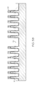
- a substrate 10 is shown. Initially, a set of trenches 12 will be etched to yield a set of fins 14 . Then, as shown in FIG. 2 , a multi-layer STI liner will be formed over the etched substrate. Specifically, a first liner layer 16 will be applied over fins 14 , and a second liner layer 18 will be applied over first liner layer 16 .
- First liner layer 16 may be an ISSG liner to repair any Si surface damage post etching (e.g., to reduce leakage current).
- Second liner layer 18 generally is a protective liner to protect the SiN hard mask and pad oxide during/following the eHARP removal process. Along these lines, second liner layer 18 may be SiN or Poly-Si.
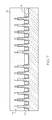
- an eHARP fill 20 is performed over second liner layer 18 and subsequently polished (e.g., via CMP). Then, as shown in FIG. 4 , eHARP fill 20 is etched back to a lower level along fins 14 .
- FIGS. 5A-B shows two removal processes for second liner layer 18 depending on the material used.
- FIG. 5A shows the removal of SiN second liner layer 18 from above eHARP material 20 along fins 14 . In general, this may be accomplished using hot phosphorous techniques to remove liner layer 18 , but keep the pad SiN as shown. Due to high selectivity between SiN and oxide remove rates (in hot phosphorous treatments), the ISSG liner 16 will remain after the SiN liner 18 removal.
- FIG. 5B shows the removal of a poly-silicon second liner layer 18 from the device. In this embodiment, when poly-silicon is used as a second liner layer instead of SiN) the device may be subjected to direct thermal treatment to oxidize the layer (now shown as oxidized layer 22 ).
- FIG. 6A the device of FIG. 5A is shown after HDP refill 24 .
- FIG. 6A shows HDP refill 24 over remaining liner layer 18 and eHARP fill 20 .
- FIG. 6B shows the device of FIG. 5B after HDP refill 24 .
- FIG. 6B shows HDP refill 24 over oxidized layer 22 and eHARP fill 20 .
- FIG. 7 shows the device of FIG. 6A after HDP refill 24 has been polished (and/or etched) back to a top surface of fins 14 .
- the device of FIG. 6B could be etched back in a similar manner.
- FIG. 8 shows the deposition (e.g., etch stop deposition) of a silicon layer 26 after the SiN second liner layer 18 of has been removed in accordance with FIG. 5A .
- silicon layer 26 is a thin silicon layer applied using etch stop deposition. Due to high selectivity between Si to SiN and oxide removal rates, the “thin” silicon layer 26 will serve as a protective layer during downstream wet/dry clean processes.
- FIG. 9 shows the subsequent HDP refill 24 over silicon layer 26 and eHARP fill 20 (e.g., similar to FIGS. 6A-B ). HDP refill is then polished and etched back as shown in FIG. 10 and FIG. 11 , respectively.
- design tools can be provided and configured to create the data sets used to pattern the semiconductor layers as described herein. For example, data sets can be created to generate photomasks used during lithography operations to pattern the layers for structures as described herein.
- Such design tools can include a collection of one or more modules and can also include hardware, software, or a combination thereof.
- a tool can be a collection of one or more software modules, hardware modules, software/hardware modules, or any combination or permutation thereof.
- a tool can be a computing device or other appliance on which software runs or in which hardware is implemented.
- a module might be implemented utilizing any form of hardware, software, or a combination thereof.
- processors for example, one or more processors, controllers, application-specific integrated circuits (ASIC), programmable logic arrays (PLA)s, logical components, software routines, or other mechanisms might be implemented to make up a module.
- ASIC application-specific integrated circuits
- PDA programmable logic arrays
- logical components software routines, or other mechanisms might be implemented to make up a module.
- the various modules described herein might be implemented as discrete modules or the functions and features described can be shared in part or in total among one or more modules.
- the various features and functionality described herein may be implemented in any given application and can be implemented in one or more separate or shared modules in various combinations and permutations.
Landscapes
- Element Separation (AREA)
Abstract
Description
Claims (19)
Priority Applications (2)
| Application Number | Priority Date | Filing Date | Title |
|---|---|---|---|
| US13/765,723 US9123771B2 (en) | 2013-02-13 | 2013-02-13 | Shallow trench isolation integration methods and devices formed thereby |
| US14/810,167 US9385192B2 (en) | 2013-02-13 | 2015-07-27 | Shallow trench isolation integration methods and devices formed thereby |
Applications Claiming Priority (1)
| Application Number | Priority Date | Filing Date | Title |
|---|---|---|---|
| US13/765,723 US9123771B2 (en) | 2013-02-13 | 2013-02-13 | Shallow trench isolation integration methods and devices formed thereby |
Related Child Applications (1)
| Application Number | Title | Priority Date | Filing Date |
|---|---|---|---|
| US14/810,167 Continuation US9385192B2 (en) | 2013-02-13 | 2015-07-27 | Shallow trench isolation integration methods and devices formed thereby |
Publications (2)
| Publication Number | Publication Date |
|---|---|
| US20140227858A1 US20140227858A1 (en) | 2014-08-14 |
| US9123771B2 true US9123771B2 (en) | 2015-09-01 |
Family
ID=51297718
Family Applications (2)
| Application Number | Title | Priority Date | Filing Date |
|---|---|---|---|
| US13/765,723 Active US9123771B2 (en) | 2013-02-13 | 2013-02-13 | Shallow trench isolation integration methods and devices formed thereby |
| US14/810,167 Active US9385192B2 (en) | 2013-02-13 | 2015-07-27 | Shallow trench isolation integration methods and devices formed thereby |
Family Applications After (1)
| Application Number | Title | Priority Date | Filing Date |
|---|---|---|---|
| US14/810,167 Active US9385192B2 (en) | 2013-02-13 | 2015-07-27 | Shallow trench isolation integration methods and devices formed thereby |
Country Status (1)
| Country | Link |
|---|---|
| US (2) | US9123771B2 (en) |
Cited By (5)
| Publication number | Priority date | Publication date | Assignee | Title |
|---|---|---|---|---|
| US9601626B2 (en) * | 2015-01-23 | 2017-03-21 | Taiwan Semiconductor Manufacturing Co., Ltd. | Semiconductor device including fin structure with two channel layers and manufacturing method thereof |
| US9691765B1 (en) | 2016-03-08 | 2017-06-27 | International Business Machines Corporation | Fin type field effect transistors with different pitches and substantially uniform fin reveal |
| US11127654B2 (en) | 2018-07-13 | 2021-09-21 | Samsung Electronics Co., Ltd. | Semiconductor device and a manufacturing method thereof |
| US11282921B2 (en) | 2019-10-21 | 2022-03-22 | Samsung Electronics Co., Ltd. | Semiconductor device and method of manufacturing the same |
| US20220254680A1 (en) * | 2016-06-29 | 2022-08-11 | Taiwan Semiconductor Manufacturing Co., Ltd. | Etch Stop Layer for Semiconductor Devices |
Families Citing this family (24)
| Publication number | Priority date | Publication date | Assignee | Title |
|---|---|---|---|---|
| US9087870B2 (en) * | 2013-05-29 | 2015-07-21 | GlobalFoundries, Inc. | Integrated circuits including FINFET devices with shallow trench isolation that includes a thermal oxide layer and methods for making the same |
| US9793268B2 (en) * | 2014-01-24 | 2017-10-17 | Taiwan Semiconductor Manufacturing Company, Ltd. | Method and structure for gap filling improvement |
| US20150270159A1 (en) * | 2014-03-20 | 2015-09-24 | Globalfoundries Inc. | Fabrication of semiconductor structures using oxidized polycrystalline silicon as conformal stop layers |
| US9178067B1 (en) * | 2014-04-25 | 2015-11-03 | Taiwan Semiconductor Manufacturing Company, Ltd. | Structure and method for FinFET device |
| US9419015B1 (en) * | 2015-03-13 | 2016-08-16 | Globalfoundries Inc. | Method for integrating thin-film transistors on an isolation region in an integrated circuit and resulting device |
| US10593801B2 (en) | 2015-04-10 | 2020-03-17 | Samsung Electronics Co., Ltd. | Semiconductor devices and methods of fabricating the same |
| US10818558B2 (en) | 2015-04-24 | 2020-10-27 | Taiwan Semiconductor Manufacturing Co., Ltd. | Semiconductor structure having trench and manufacturing method thereof |
| US9680017B2 (en) * | 2015-09-16 | 2017-06-13 | Taiwan Semiconductor Manufacturing Co., Ltd. | Semiconductor device including Fin FET and manufacturing method thereof |
| US9490253B1 (en) * | 2015-09-23 | 2016-11-08 | International Business Machines Corporation | Gate planarity for finFET using dummy polish stop |
| US9722053B1 (en) * | 2016-03-21 | 2017-08-01 | Globalfoundries Inc. | Methods, apparatus and system for local isolation formation for finFET devices |
| US9536793B1 (en) * | 2016-04-22 | 2017-01-03 | Globalfoundries Inc. | Self-aligned gate-first VFETs using a gate spacer recess |
| CN107346740B (en) * | 2016-05-05 | 2020-06-09 | 中芯国际集成电路制造(上海)有限公司 | Fin type field effect transistor and forming method thereof |
| US9799749B1 (en) * | 2016-08-18 | 2017-10-24 | International Business Machines Corporation | Vertical transport FET devices with uniform bottom spacer |
| US10141305B2 (en) * | 2016-09-15 | 2018-11-27 | Qualcomm Incorporated | Semiconductor devices employing field effect transistors (FETs) with multiple channel structures without shallow trench isolation (STI) void-induced electrical shorts |
| US9953879B1 (en) * | 2016-10-03 | 2018-04-24 | Globalfoundries Inc. | Preventing oxidation defects in strain-relaxed fins by reducing local gap fill voids |
| US10297597B2 (en) | 2016-10-03 | 2019-05-21 | Globalfoundries Inc. | Composite isolation structures for a fin-type field effect transistor |
| KR20180071101A (en) * | 2016-12-19 | 2018-06-27 | 삼성전자주식회사 | semiconductor device and method for manufacturing the same |
| CN108735750B (en) * | 2017-04-19 | 2021-04-20 | 华邦电子股份有限公司 | Memory structure and method of making the same |
| CN108933105B (en) * | 2017-05-24 | 2020-11-03 | 中芯国际集成电路制造(上海)有限公司 | Semiconductor structure and forming method thereof |
| US10468501B2 (en) | 2017-09-29 | 2019-11-05 | Taiwan Semiconductor Manufacturing Company, Ltd. | Gap-filling germanium through selective bottom-up growth |
| US10510874B2 (en) | 2017-11-30 | 2019-12-17 | Taiwan Semiconductor Manufacturing Co., Ltd. | Semiconductor device |
| KR102541010B1 (en) | 2018-07-12 | 2023-06-07 | 삼성전자주식회사 | Semiconductor devices |
| US11211470B2 (en) * | 2019-10-18 | 2021-12-28 | Taiwan Semiconductor Manufacturing Company, Ltd. | Semiconductor device and method |
| US11309433B2 (en) * | 2020-03-18 | 2022-04-19 | Winbond Electronics Corp. | Non-volatile memory structure and manufacturing method thereof |
Citations (7)
| Publication number | Priority date | Publication date | Assignee | Title |
|---|---|---|---|---|
| US20050167778A1 (en) * | 2004-02-03 | 2005-08-04 | Shin-Hye Kim | Shallow trench isolation structure with converted liner layer |
| US20050266647A1 (en) * | 2004-05-25 | 2005-12-01 | Kim Tae-Hyun | Method of manufacturing a semiconductor device |
| US20070205489A1 (en) * | 2006-03-01 | 2007-09-06 | Armin Tilke | Methods of fabricating isolation regions of semiconductor devices and structures thereof |
| US20080217702A1 (en) * | 2006-08-04 | 2008-09-11 | Kabushiki Kaisha Toshiba | Semiconductor device and method of fabricating isolation region |
| US20090029556A1 (en) * | 2007-07-24 | 2009-01-29 | Chien-Mao Liao | Method for forming a shallow trench isolation |
| US20120178235A1 (en) * | 2011-01-12 | 2012-07-12 | Jayavel Pachamuthu | Air Isolation In High Density Non-Volatile Memory |
| US8329552B1 (en) * | 2011-07-22 | 2012-12-11 | Taiwan Semiconductor Manufacturing Company, Ltd. | Semiconductor device and method of manufacture |
Family Cites Families (1)
| Publication number | Priority date | Publication date | Assignee | Title |
|---|---|---|---|---|
| US7811935B2 (en) * | 2006-03-07 | 2010-10-12 | Micron Technology, Inc. | Isolation regions and their formation |
-
2013
- 2013-02-13 US US13/765,723 patent/US9123771B2/en active Active
-
2015
- 2015-07-27 US US14/810,167 patent/US9385192B2/en active Active
Patent Citations (7)
| Publication number | Priority date | Publication date | Assignee | Title |
|---|---|---|---|---|
| US20050167778A1 (en) * | 2004-02-03 | 2005-08-04 | Shin-Hye Kim | Shallow trench isolation structure with converted liner layer |
| US20050266647A1 (en) * | 2004-05-25 | 2005-12-01 | Kim Tae-Hyun | Method of manufacturing a semiconductor device |
| US20070205489A1 (en) * | 2006-03-01 | 2007-09-06 | Armin Tilke | Methods of fabricating isolation regions of semiconductor devices and structures thereof |
| US20080217702A1 (en) * | 2006-08-04 | 2008-09-11 | Kabushiki Kaisha Toshiba | Semiconductor device and method of fabricating isolation region |
| US20090029556A1 (en) * | 2007-07-24 | 2009-01-29 | Chien-Mao Liao | Method for forming a shallow trench isolation |
| US20120178235A1 (en) * | 2011-01-12 | 2012-07-12 | Jayavel Pachamuthu | Air Isolation In High Density Non-Volatile Memory |
| US8329552B1 (en) * | 2011-07-22 | 2012-12-11 | Taiwan Semiconductor Manufacturing Company, Ltd. | Semiconductor device and method of manufacture |
Cited By (13)
| Publication number | Priority date | Publication date | Assignee | Title |
|---|---|---|---|---|
| US9966469B2 (en) | 2015-01-23 | 2018-05-08 | Taiwan Semiconductor Manufacturing Co., Ltd. | Semiconductor device including fin structure with two channel layers and manufacturing method thereof |
| US10326023B2 (en) | 2015-01-23 | 2019-06-18 | Taiwan Semiconductor Manufacturing Co., Ltd. | Semiconductor device including fin structure with two channel layers and manufacturing method thereof |
| US9601626B2 (en) * | 2015-01-23 | 2017-03-21 | Taiwan Semiconductor Manufacturing Co., Ltd. | Semiconductor device including fin structure with two channel layers and manufacturing method thereof |
| US9691765B1 (en) | 2016-03-08 | 2017-06-27 | International Business Machines Corporation | Fin type field effect transistors with different pitches and substantially uniform fin reveal |
| US10020229B2 (en) | 2016-03-08 | 2018-07-10 | International Business Machines Corporation | Fin type field effect transistors with different pitches and substantially uniform fin reveal |
| US10388571B2 (en) | 2016-03-08 | 2019-08-20 | International Business Machines Corporation | Fin type field effect transistors with different pitches and substantially uniform fin reveal |
| US20220254680A1 (en) * | 2016-06-29 | 2022-08-11 | Taiwan Semiconductor Manufacturing Co., Ltd. | Etch Stop Layer for Semiconductor Devices |
| US12451393B2 (en) * | 2016-06-29 | 2025-10-21 | Taiwan Semiconductor Manufacturing Co., Ltd. | Etch stop layer for semiconductor devices |
| US11127654B2 (en) | 2018-07-13 | 2021-09-21 | Samsung Electronics Co., Ltd. | Semiconductor device and a manufacturing method thereof |
| US12199014B2 (en) | 2018-07-13 | 2025-01-14 | Samsung Electronics Co., Ltd. | Semiconductor device and a manufacturing method thereof |
| US11735626B2 (en) | 2019-10-21 | 2023-08-22 | Samsung Electronics Co., Ltd. | Semiconductor device and method of manufacturing the same |
| US12034042B2 (en) | 2019-10-21 | 2024-07-09 | Samsung Electronics Co., Ltd. | Method of manufacturing multi-channel field effect transistors |
| US11282921B2 (en) | 2019-10-21 | 2022-03-22 | Samsung Electronics Co., Ltd. | Semiconductor device and method of manufacturing the same |
Also Published As
| Publication number | Publication date |
|---|---|
| US9385192B2 (en) | 2016-07-05 |
| US20150333121A1 (en) | 2015-11-19 |
| US20140227858A1 (en) | 2014-08-14 |
Similar Documents
| Publication | Publication Date | Title |
|---|---|---|
| US9123771B2 (en) | Shallow trench isolation integration methods and devices formed thereby | |
| TWI688097B (en) | Asymmetric formation of epi semiconductor material in source/drain regions of finfet devices | |
| CN105826193A (en) | Formation method of semiconductor device | |
| US9196499B2 (en) | Method of forming semiconductor fins | |
| US8722491B2 (en) | Replacement metal gate semiconductor device formation using low resistivity metals | |
| US9520395B2 (en) | FinFET devices comprising a dielectric layer/CMP stop layer/hardmask/etch stop layer/gap-fill material stack | |
| CN105719997B (en) | Formation method of semiconductor structure | |
| CN102412140A (en) | Reduced non-uniformity in semiconductor planarization | |
| US20160372425A1 (en) | Through silicon via device having low stress, thin film gaps and methods for forming the same | |
| CN106684030A (en) | Manufacturing method of shallow groove isolation structure | |
| US20180097089A1 (en) | Devices and methods of forming unmerged epitaxy for finfet device | |
| US20140145257A1 (en) | Semiconductor device having a metal recess | |
| US20150200111A1 (en) | Planarization scheme for finfet gate height uniformity control | |
| US10049887B2 (en) | Method of planarizing substrate surface | |
| US20150050792A1 (en) | Extra narrow diffusion break for 3d finfet technologies | |
| CN108878288B (en) | Manufacturing method of interlayer film | |
| CN104465489B (en) | Semiconductor devices and forming method thereof | |
| US20150140819A1 (en) | Semiconductor process | |
| CN109686702B (en) | Semiconductor structure and method of forming the same | |
| US10062572B2 (en) | Semiconductor structure and fabrication method thereof | |
| US20130214392A1 (en) | Methods of forming stepped isolation structures for semiconductor devices using a spacer technique | |
| CN111696867A (en) | Semiconductor structure and forming method | |
| TW201428829A (en) | Semiconductor device manufacturing method | |
| US8716094B1 (en) | FinFET formation using double patterning memorization | |
| TWI733013B (en) | Semiconductor fabrication method |
Legal Events
| Date | Code | Title | Description |
|---|---|---|---|
| AS | Assignment |
Owner name: GLOBALFOUNDRIES INC., CAYMAN ISLANDS Free format text: ASSIGNMENT OF ASSIGNORS INTEREST;ASSIGNORS:SHEN, HONGLIANG;NA, KYUTAE;GAAN, SANDEEP;AND OTHERS;SIGNING DATES FROM 20130107 TO 20130206;REEL/FRAME:029802/0535 |
|
| STCF | Information on status: patent grant |
Free format text: PATENTED CASE |
|
| AS | Assignment |
Owner name: WILMINGTON TRUST, NATIONAL ASSOCIATION, DELAWARE Free format text: SECURITY AGREEMENT;ASSIGNOR:GLOBALFOUNDRIES INC.;REEL/FRAME:049490/0001 Effective date: 20181127 |
|
| MAFP | Maintenance fee payment |
Free format text: PAYMENT OF MAINTENANCE FEE, 4TH YEAR, LARGE ENTITY (ORIGINAL EVENT CODE: M1551); ENTITY STATUS OF PATENT OWNER: LARGE ENTITY Year of fee payment: 4 |
|
| AS | Assignment |
Owner name: GLOBALFOUNDRIES U.S. INC., CALIFORNIA Free format text: ASSIGNMENT OF ASSIGNORS INTEREST;ASSIGNOR:GLOBALFOUNDRIES INC.;REEL/FRAME:054633/0001 Effective date: 20201022 |
|
| AS | Assignment |
Owner name: GLOBALFOUNDRIES INC., CAYMAN ISLANDS Free format text: RELEASE BY SECURED PARTY;ASSIGNOR:WILMINGTON TRUST, NATIONAL ASSOCIATION;REEL/FRAME:054636/0001 Effective date: 20201117 |
|
| AS | Assignment |
Owner name: GLOBALFOUNDRIES U.S. INC., NEW YORK Free format text: RELEASE BY SECURED PARTY;ASSIGNOR:WILMINGTON TRUST, NATIONAL ASSOCIATION;REEL/FRAME:056987/0001 Effective date: 20201117 Owner name: GLOBALFOUNDRIES U.S. INC., NEW YORK Free format text: RELEASE OF SECURITY INTEREST;ASSIGNOR:WILMINGTON TRUST, NATIONAL ASSOCIATION;REEL/FRAME:056987/0001 Effective date: 20201117 |
|
| MAFP | Maintenance fee payment |
Free format text: PAYMENT OF MAINTENANCE FEE, 8TH YEAR, LARGE ENTITY (ORIGINAL EVENT CODE: M1552); ENTITY STATUS OF PATENT OWNER: LARGE ENTITY Year of fee payment: 8 |