US9123763B2 - Package-on-package (PoP) structure having at least one package comprising one die being disposed in a core material between first and second surfaces of the core material - Google Patents
Package-on-package (PoP) structure having at least one package comprising one die being disposed in a core material between first and second surfaces of the core material Download PDFInfo
- Publication number
- US9123763B2 US9123763B2 US13/271,952 US201113271952A US9123763B2 US 9123763 B2 US9123763 B2 US 9123763B2 US 201113271952 A US201113271952 A US 201113271952A US 9123763 B2 US9123763 B2 US 9123763B2
- Authority
- US
- United States
- Prior art keywords
- die
- package
- rdl
- core material
- substrate
- Prior art date
- Legal status (The legal status is an assumption and is not a legal conclusion. Google has not performed a legal analysis and makes no representation as to the accuracy of the status listed.)
- Active, expires
Links
Images


Classifications
-
- H01L21/6835—
-
- H01L21/568—
-
- H01L23/5383—
-
- H01L25/105—
-
- H—ELECTRICITY
- H10—SEMICONDUCTOR DEVICES; ELECTRIC SOLID-STATE DEVICES NOT OTHERWISE PROVIDED FOR
- H10P—GENERIC PROCESSES OR APPARATUS FOR THE MANUFACTURE OR TREATMENT OF DEVICES COVERED BY CLASS H10
- H10P72/00—Handling or holding of wafers, substrates or devices during manufacture or treatment thereof
- H10P72/70—Handling or holding of wafers, substrates or devices during manufacture or treatment thereof for supporting or gripping
- H10P72/74—Handling or holding of wafers, substrates or devices during manufacture or treatment thereof for supporting or gripping using temporarily an auxiliary support
-
- H—ELECTRICITY
- H10—SEMICONDUCTOR DEVICES; ELECTRIC SOLID-STATE DEVICES NOT OTHERWISE PROVIDED FOR
- H10P—GENERIC PROCESSES OR APPARATUS FOR THE MANUFACTURE OR TREATMENT OF DEVICES COVERED BY CLASS H10
- H10P95/00—Generic processes or apparatus for manufacture or treatments not covered by the other groups of this subclass
- H10P95/06—Planarisation of inorganic insulating materials
-
- H—ELECTRICITY
- H10—SEMICONDUCTOR DEVICES; ELECTRIC SOLID-STATE DEVICES NOT OTHERWISE PROVIDED FOR
- H10W—GENERIC PACKAGES, INTERCONNECTIONS, CONNECTORS OR OTHER CONSTRUCTIONAL DETAILS OF DEVICES COVERED BY CLASS H10
- H10W20/00—Interconnections in chips, wafers or substrates
- H10W20/01—Manufacture or treatment
- H10W20/021—Manufacture or treatment of interconnections within wafers or substrates
- H10W20/023—Manufacture or treatment of interconnections within wafers or substrates the interconnections being through-semiconductor vias
-
- H—ELECTRICITY
- H10—SEMICONDUCTOR DEVICES; ELECTRIC SOLID-STATE DEVICES NOT OTHERWISE PROVIDED FOR
- H10W—GENERIC PACKAGES, INTERCONNECTIONS, CONNECTORS OR OTHER CONSTRUCTIONAL DETAILS OF DEVICES COVERED BY CLASS H10
- H10W20/00—Interconnections in chips, wafers or substrates
- H10W20/01—Manufacture or treatment
- H10W20/031—Manufacture or treatment of conductive parts of the interconnections
- H10W20/056—Manufacture or treatment of conductive parts of the interconnections by filling conductive material into holes, grooves or trenches
-
- H—ELECTRICITY
- H10—SEMICONDUCTOR DEVICES; ELECTRIC SOLID-STATE DEVICES NOT OTHERWISE PROVIDED FOR
- H10W—GENERIC PACKAGES, INTERCONNECTIONS, CONNECTORS OR OTHER CONSTRUCTIONAL DETAILS OF DEVICES COVERED BY CLASS H10
- H10W20/00—Interconnections in chips, wafers or substrates
- H10W20/01—Manufacture or treatment
- H10W20/071—Manufacture or treatment of dielectric parts thereof
- H10W20/081—Manufacture or treatment of dielectric parts thereof by forming openings in the dielectric parts
-
- H—ELECTRICITY
- H10—SEMICONDUCTOR DEVICES; ELECTRIC SOLID-STATE DEVICES NOT OTHERWISE PROVIDED FOR
- H10W—GENERIC PACKAGES, INTERCONNECTIONS, CONNECTORS OR OTHER CONSTRUCTIONAL DETAILS OF DEVICES COVERED BY CLASS H10
- H10W20/00—Interconnections in chips, wafers or substrates
- H10W20/01—Manufacture or treatment
- H10W20/071—Manufacture or treatment of dielectric parts thereof
- H10W20/092—Manufacture or treatment of dielectric parts thereof by smoothing the dielectric parts
-
- H—ELECTRICITY
- H10—SEMICONDUCTOR DEVICES; ELECTRIC SOLID-STATE DEVICES NOT OTHERWISE PROVIDED FOR
- H10W—GENERIC PACKAGES, INTERCONNECTIONS, CONNECTORS OR OTHER CONSTRUCTIONAL DETAILS OF DEVICES COVERED BY CLASS H10
- H10W70/00—Package substrates; Interposers; Redistribution layers [RDL]
- H10W70/01—Manufacture or treatment
- H10W70/05—Manufacture or treatment of insulating or insulated package substrates, or of interposers, or of redistribution layers
- H10W70/08—Manufacture or treatment of insulating or insulated package substrates, or of interposers, or of redistribution layers by depositing layers on the chip or wafer, e.g. "chip-first" RDLs
- H10W70/09—Manufacture or treatment of insulating or insulated package substrates, or of interposers, or of redistribution layers by depositing layers on the chip or wafer, e.g. "chip-first" RDLs extending onto an encapsulation that laterally surrounds the chip or wafer, e.g. fan-out wafer level package [FOWLP] RDLs
-
- H—ELECTRICITY
- H10—SEMICONDUCTOR DEVICES; ELECTRIC SOLID-STATE DEVICES NOT OTHERWISE PROVIDED FOR
- H10W—GENERIC PACKAGES, INTERCONNECTIONS, CONNECTORS OR OTHER CONSTRUCTIONAL DETAILS OF DEVICES COVERED BY CLASS H10
- H10W70/00—Package substrates; Interposers; Redistribution layers [RDL]
- H10W70/01—Manufacture or treatment
- H10W70/05—Manufacture or treatment of insulating or insulated package substrates, or of interposers, or of redistribution layers
- H10W70/093—Connecting or disconnecting other interconnections thereto or therefrom, e.g. connecting bond wires or bumps
-
- H—ELECTRICITY
- H10—SEMICONDUCTOR DEVICES; ELECTRIC SOLID-STATE DEVICES NOT OTHERWISE PROVIDED FOR
- H10W—GENERIC PACKAGES, INTERCONNECTIONS, CONNECTORS OR OTHER CONSTRUCTIONAL DETAILS OF DEVICES COVERED BY CLASS H10
- H10W70/00—Package substrates; Interposers; Redistribution layers [RDL]
- H10W70/60—Insulating or insulated package substrates; Interposers; Redistribution layers
- H10W70/611—Insulating or insulated package substrates; Interposers; Redistribution layers for connecting multiple chips together
-
- H—ELECTRICITY
- H10—SEMICONDUCTOR DEVICES; ELECTRIC SOLID-STATE DEVICES NOT OTHERWISE PROVIDED FOR
- H10W—GENERIC PACKAGES, INTERCONNECTIONS, CONNECTORS OR OTHER CONSTRUCTIONAL DETAILS OF DEVICES COVERED BY CLASS H10
- H10W70/00—Package substrates; Interposers; Redistribution layers [RDL]
- H10W70/60—Insulating or insulated package substrates; Interposers; Redistribution layers
- H10W70/67—Insulating or insulated package substrates; Interposers; Redistribution layers characterised by their insulating layers or insulating parts
- H10W70/68—Shapes or dispositions thereof
- H10W70/685—Shapes or dispositions thereof comprising multiple insulating layers
-
- H—ELECTRICITY
- H10—SEMICONDUCTOR DEVICES; ELECTRIC SOLID-STATE DEVICES NOT OTHERWISE PROVIDED FOR
- H10W—GENERIC PACKAGES, INTERCONNECTIONS, CONNECTORS OR OTHER CONSTRUCTIONAL DETAILS OF DEVICES COVERED BY CLASS H10
- H10W74/00—Encapsulations, e.g. protective coatings
- H10W74/01—Manufacture or treatment
- H10W74/016—Manufacture or treatment using moulds
-
- H—ELECTRICITY
- H10—SEMICONDUCTOR DEVICES; ELECTRIC SOLID-STATE DEVICES NOT OTHERWISE PROVIDED FOR
- H10W—GENERIC PACKAGES, INTERCONNECTIONS, CONNECTORS OR OTHER CONSTRUCTIONAL DETAILS OF DEVICES COVERED BY CLASS H10
- H10W74/00—Encapsulations, e.g. protective coatings
- H10W74/01—Manufacture or treatment
- H10W74/019—Manufacture or treatment using temporary auxiliary substrates
-
- H—ELECTRICITY
- H10—SEMICONDUCTOR DEVICES; ELECTRIC SOLID-STATE DEVICES NOT OTHERWISE PROVIDED FOR
- H10W—GENERIC PACKAGES, INTERCONNECTIONS, CONNECTORS OR OTHER CONSTRUCTIONAL DETAILS OF DEVICES COVERED BY CLASS H10
- H10W90/00—Package configurations
-
- H01L21/4846—
-
- H01L2221/68345—
-
- H01L2224/13082—
-
- H01L2224/131—
-
- H01L2224/16225—
-
- H01L2224/16237—
-
- H01L2224/2919—
-
- H01L2224/32145—
-
- H01L2224/32225—
-
- H01L2224/45124—
-
- H01L2224/45144—
-
- H01L2224/48—
-
- H01L2224/73204—
-
- H01L2224/73253—
-
- H01L2224/81005—
-
- H01L2224/81191—
-
- H01L2224/81815—
-
- H01L2224/83104—
-
- H01L2225/1023—
-
- H01L2225/1058—
-
- H01L23/3128—
-
- H01L23/49816—
-
- H01L23/49822—
-
- H01L23/49827—
-
- H01L24/16—
-
- H01L24/32—
-
- H01L2924/00—
-
- H01L2924/00012—
-
- H01L2924/00014—
-
- H01L2924/014—
-
- H01L2924/0665—
-
- H01L2924/15311—
-
- H01L2924/15331—
-
- H—ELECTRICITY
- H05—ELECTRIC TECHNIQUES NOT OTHERWISE PROVIDED FOR
- H05K—PRINTED CIRCUITS; CASINGS OR CONSTRUCTIONAL DETAILS OF ELECTRIC APPARATUS; MANUFACTURE OF ASSEMBLAGES OF ELECTRICAL COMPONENTS
- H05K1/00—Printed circuits
- H05K1/18—Printed circuits structurally associated with non-printed electric components
- H05K1/182—Printed circuits structurally associated with non-printed electric components associated with components mounted in printed circuit boards [PCB], e.g. insert-mounted components [IMC]
- H05K1/185—Printed circuits structurally associated with non-printed electric components associated with components mounted in printed circuit boards [PCB], e.g. insert-mounted components [IMC] associated with components encapsulated in the insulating substrate of the PCBs; associated with components incorporated in internal layers of multilayer circuit boards
-
- H—ELECTRICITY
- H10—SEMICONDUCTOR DEVICES; ELECTRIC SOLID-STATE DEVICES NOT OTHERWISE PROVIDED FOR
- H10P—GENERIC PROCESSES OR APPARATUS FOR THE MANUFACTURE OR TREATMENT OF DEVICES COVERED BY CLASS H10
- H10P72/00—Handling or holding of wafers, substrates or devices during manufacture or treatment thereof
- H10P72/70—Handling or holding of wafers, substrates or devices during manufacture or treatment thereof for supporting or gripping
- H10P72/74—Handling or holding of wafers, substrates or devices during manufacture or treatment thereof for supporting or gripping using temporarily an auxiliary support
- H10P72/7424—Handling or holding of wafers, substrates or devices during manufacture or treatment thereof for supporting or gripping using temporarily an auxiliary support used as a support during the manufacture of self-supporting substrates
-
- H—ELECTRICITY
- H10—SEMICONDUCTOR DEVICES; ELECTRIC SOLID-STATE DEVICES NOT OTHERWISE PROVIDED FOR
- H10W—GENERIC PACKAGES, INTERCONNECTIONS, CONNECTORS OR OTHER CONSTRUCTIONAL DETAILS OF DEVICES COVERED BY CLASS H10
- H10W70/00—Package substrates; Interposers; Redistribution layers [RDL]
- H10W70/60—Insulating or insulated package substrates; Interposers; Redistribution layers
- H10W70/62—Insulating or insulated package substrates; Interposers; Redistribution layers characterised by their interconnections
- H10W70/63—Vias, e.g. via plugs
- H10W70/635—Through-vias
-
- H—ELECTRICITY
- H10—SEMICONDUCTOR DEVICES; ELECTRIC SOLID-STATE DEVICES NOT OTHERWISE PROVIDED FOR
- H10W—GENERIC PACKAGES, INTERCONNECTIONS, CONNECTORS OR OTHER CONSTRUCTIONAL DETAILS OF DEVICES COVERED BY CLASS H10
- H10W72/00—Interconnections or connectors in packages
- H10W72/071—Connecting or disconnecting
- H10W72/072—Connecting or disconnecting of bump connectors
- H10W72/07202—Connecting or disconnecting of bump connectors using auxiliary members
- H10W72/07204—Connecting or disconnecting of bump connectors using auxiliary members using temporary auxiliary members, e.g. sacrificial coatings
- H10W72/07207—Temporary substrates, e.g. removable substrates
-
- H—ELECTRICITY
- H10—SEMICONDUCTOR DEVICES; ELECTRIC SOLID-STATE DEVICES NOT OTHERWISE PROVIDED FOR
- H10W—GENERIC PACKAGES, INTERCONNECTIONS, CONNECTORS OR OTHER CONSTRUCTIONAL DETAILS OF DEVICES COVERED BY CLASS H10
- H10W72/00—Interconnections or connectors in packages
- H10W72/071—Connecting or disconnecting
- H10W72/072—Connecting or disconnecting of bump connectors
- H10W72/07231—Techniques
- H10W72/07236—Soldering or alloying
-
- H—ELECTRICITY
- H10—SEMICONDUCTOR DEVICES; ELECTRIC SOLID-STATE DEVICES NOT OTHERWISE PROVIDED FOR
- H10W—GENERIC PACKAGES, INTERCONNECTIONS, CONNECTORS OR OTHER CONSTRUCTIONAL DETAILS OF DEVICES COVERED BY CLASS H10
- H10W72/00—Interconnections or connectors in packages
- H10W72/071—Connecting or disconnecting
- H10W72/073—Connecting or disconnecting of die-attach connectors
-
- H—ELECTRICITY
- H10—SEMICONDUCTOR DEVICES; ELECTRIC SOLID-STATE DEVICES NOT OTHERWISE PROVIDED FOR
- H10W—GENERIC PACKAGES, INTERCONNECTIONS, CONNECTORS OR OTHER CONSTRUCTIONAL DETAILS OF DEVICES COVERED BY CLASS H10
- H10W72/00—Interconnections or connectors in packages
- H10W72/20—Bump connectors, e.g. solder bumps or copper pillars; Dummy bumps; Thermal bumps
- H10W72/221—Structures or relative sizes
- H10W72/222—Multilayered bumps, e.g. a coating on top and side surfaces of a bump core
-
- H—ELECTRICITY
- H10—SEMICONDUCTOR DEVICES; ELECTRIC SOLID-STATE DEVICES NOT OTHERWISE PROVIDED FOR
- H10W—GENERIC PACKAGES, INTERCONNECTIONS, CONNECTORS OR OTHER CONSTRUCTIONAL DETAILS OF DEVICES COVERED BY CLASS H10
- H10W72/00—Interconnections or connectors in packages
- H10W72/20—Bump connectors, e.g. solder bumps or copper pillars; Dummy bumps; Thermal bumps
- H10W72/241—Dispositions, e.g. layouts
-
- H—ELECTRICITY
- H10—SEMICONDUCTOR DEVICES; ELECTRIC SOLID-STATE DEVICES NOT OTHERWISE PROVIDED FOR
- H10W—GENERIC PACKAGES, INTERCONNECTIONS, CONNECTORS OR OTHER CONSTRUCTIONAL DETAILS OF DEVICES COVERED BY CLASS H10
- H10W72/00—Interconnections or connectors in packages
- H10W72/20—Bump connectors, e.g. solder bumps or copper pillars; Dummy bumps; Thermal bumps
- H10W72/251—Materials
- H10W72/252—Materials comprising solid metals or solid metalloids, e.g. PbSn, Ag or Cu
-
- H—ELECTRICITY
- H10—SEMICONDUCTOR DEVICES; ELECTRIC SOLID-STATE DEVICES NOT OTHERWISE PROVIDED FOR
- H10W—GENERIC PACKAGES, INTERCONNECTIONS, CONNECTORS OR OTHER CONSTRUCTIONAL DETAILS OF DEVICES COVERED BY CLASS H10
- H10W72/00—Interconnections or connectors in packages
- H10W72/30—Die-attach connectors
- H10W72/351—Materials of die-attach connectors
- H10W72/353—Materials of die-attach connectors not comprising solid metals or solid metalloids, e.g. ceramics
- H10W72/354—Materials of die-attach connectors not comprising solid metals or solid metalloids, e.g. ceramics comprising polymers
-
- H—ELECTRICITY
- H10—SEMICONDUCTOR DEVICES; ELECTRIC SOLID-STATE DEVICES NOT OTHERWISE PROVIDED FOR
- H10W—GENERIC PACKAGES, INTERCONNECTIONS, CONNECTORS OR OTHER CONSTRUCTIONAL DETAILS OF DEVICES COVERED BY CLASS H10
- H10W72/00—Interconnections or connectors in packages
- H10W72/50—Bond wires
- H10W72/551—Materials of bond wires
- H10W72/552—Materials of bond wires comprising metals or metalloids, e.g. silver
- H10W72/5522—Materials of bond wires comprising metals or metalloids, e.g. silver comprising gold [Au]
-
- H—ELECTRICITY
- H10—SEMICONDUCTOR DEVICES; ELECTRIC SOLID-STATE DEVICES NOT OTHERWISE PROVIDED FOR
- H10W—GENERIC PACKAGES, INTERCONNECTIONS, CONNECTORS OR OTHER CONSTRUCTIONAL DETAILS OF DEVICES COVERED BY CLASS H10
- H10W72/00—Interconnections or connectors in packages
- H10W72/50—Bond wires
- H10W72/551—Materials of bond wires
- H10W72/552—Materials of bond wires comprising metals or metalloids, e.g. silver
- H10W72/5524—Materials of bond wires comprising metals or metalloids, e.g. silver comprising aluminium [Al]
-
- H—ELECTRICITY
- H10—SEMICONDUCTOR DEVICES; ELECTRIC SOLID-STATE DEVICES NOT OTHERWISE PROVIDED FOR
- H10W—GENERIC PACKAGES, INTERCONNECTIONS, CONNECTORS OR OTHER CONSTRUCTIONAL DETAILS OF DEVICES COVERED BY CLASS H10
- H10W72/00—Interconnections or connectors in packages
- H10W72/823—Interconnections through encapsulations, e.g. pillars through molded resin on a lateral side a chip
-
- H—ELECTRICITY
- H10—SEMICONDUCTOR DEVICES; ELECTRIC SOLID-STATE DEVICES NOT OTHERWISE PROVIDED FOR
- H10W—GENERIC PACKAGES, INTERCONNECTIONS, CONNECTORS OR OTHER CONSTRUCTIONAL DETAILS OF DEVICES COVERED BY CLASS H10
- H10W72/00—Interconnections or connectors in packages
- H10W72/851—Dispositions of multiple connectors or interconnections
- H10W72/874—On different surfaces
- H10W72/877—Bump connectors and die-attach connectors
-
- H—ELECTRICITY
- H10—SEMICONDUCTOR DEVICES; ELECTRIC SOLID-STATE DEVICES NOT OTHERWISE PROVIDED FOR
- H10W—GENERIC PACKAGES, INTERCONNECTIONS, CONNECTORS OR OTHER CONSTRUCTIONAL DETAILS OF DEVICES COVERED BY CLASS H10
- H10W72/00—Interconnections or connectors in packages
- H10W72/90—Bond pads, in general
- H10W72/941—Dispositions of bond pads
- H10W72/9413—Dispositions of bond pads on encapsulations
-
- H—ELECTRICITY
- H10—SEMICONDUCTOR DEVICES; ELECTRIC SOLID-STATE DEVICES NOT OTHERWISE PROVIDED FOR
- H10W—GENERIC PACKAGES, INTERCONNECTIONS, CONNECTORS OR OTHER CONSTRUCTIONAL DETAILS OF DEVICES COVERED BY CLASS H10
- H10W74/00—Encapsulations, e.g. protective coatings
-
- H—ELECTRICITY
- H10—SEMICONDUCTOR DEVICES; ELECTRIC SOLID-STATE DEVICES NOT OTHERWISE PROVIDED FOR
- H10W—GENERIC PACKAGES, INTERCONNECTIONS, CONNECTORS OR OTHER CONSTRUCTIONAL DETAILS OF DEVICES COVERED BY CLASS H10
- H10W74/00—Encapsulations, e.g. protective coatings
- H10W74/10—Encapsulations, e.g. protective coatings characterised by their shape or disposition
- H10W74/111—Encapsulations, e.g. protective coatings characterised by their shape or disposition the semiconductor body being completely enclosed
- H10W74/114—Encapsulations, e.g. protective coatings characterised by their shape or disposition the semiconductor body being completely enclosed by a substrate and the encapsulations
- H10W74/117—Encapsulations, e.g. protective coatings characterised by their shape or disposition the semiconductor body being completely enclosed by a substrate and the encapsulations the substrate having spherical bumps for external connection
-
- H—ELECTRICITY
- H10—SEMICONDUCTOR DEVICES; ELECTRIC SOLID-STATE DEVICES NOT OTHERWISE PROVIDED FOR
- H10W—GENERIC PACKAGES, INTERCONNECTIONS, CONNECTORS OR OTHER CONSTRUCTIONAL DETAILS OF DEVICES COVERED BY CLASS H10
- H10W74/00—Encapsulations, e.g. protective coatings
- H10W74/10—Encapsulations, e.g. protective coatings characterised by their shape or disposition
- H10W74/15—Encapsulations, e.g. protective coatings characterised by their shape or disposition on active surfaces of flip-chip devices, e.g. underfills
-
- H—ELECTRICITY
- H10—SEMICONDUCTOR DEVICES; ELECTRIC SOLID-STATE DEVICES NOT OTHERWISE PROVIDED FOR
- H10W—GENERIC PACKAGES, INTERCONNECTIONS, CONNECTORS OR OTHER CONSTRUCTIONAL DETAILS OF DEVICES COVERED BY CLASS H10
- H10W90/00—Package configurations
- H10W90/20—Configurations of stacked chips
-
- H—ELECTRICITY
- H10—SEMICONDUCTOR DEVICES; ELECTRIC SOLID-STATE DEVICES NOT OTHERWISE PROVIDED FOR
- H10W—GENERIC PACKAGES, INTERCONNECTIONS, CONNECTORS OR OTHER CONSTRUCTIONAL DETAILS OF DEVICES COVERED BY CLASS H10
- H10W90/00—Package configurations
- H10W90/20—Configurations of stacked chips
- H10W90/22—Configurations of stacked chips the stacked chips being on both top and bottom sides of a package substrate, interposer or RDL
-
- H—ELECTRICITY
- H10—SEMICONDUCTOR DEVICES; ELECTRIC SOLID-STATE DEVICES NOT OTHERWISE PROVIDED FOR
- H10W—GENERIC PACKAGES, INTERCONNECTIONS, CONNECTORS OR OTHER CONSTRUCTIONAL DETAILS OF DEVICES COVERED BY CLASS H10
- H10W90/00—Package configurations
- H10W90/20—Configurations of stacked chips
- H10W90/288—Configurations of stacked chips characterised by arrangements for thermal management of the stacked chips
-
- H—ELECTRICITY
- H10—SEMICONDUCTOR DEVICES; ELECTRIC SOLID-STATE DEVICES NOT OTHERWISE PROVIDED FOR
- H10W—GENERIC PACKAGES, INTERCONNECTIONS, CONNECTORS OR OTHER CONSTRUCTIONAL DETAILS OF DEVICES COVERED BY CLASS H10
- H10W90/00—Package configurations
- H10W90/701—Package configurations characterised by the relative positions of pads or connectors relative to package parts
- H10W90/721—Package configurations characterised by the relative positions of pads or connectors relative to package parts of bump connectors
- H10W90/722—Package configurations characterised by the relative positions of pads or connectors relative to package parts of bump connectors between stacked chips
-
- H—ELECTRICITY
- H10—SEMICONDUCTOR DEVICES; ELECTRIC SOLID-STATE DEVICES NOT OTHERWISE PROVIDED FOR
- H10W—GENERIC PACKAGES, INTERCONNECTIONS, CONNECTORS OR OTHER CONSTRUCTIONAL DETAILS OF DEVICES COVERED BY CLASS H10
- H10W90/00—Package configurations
- H10W90/701—Package configurations characterised by the relative positions of pads or connectors relative to package parts
- H10W90/721—Package configurations characterised by the relative positions of pads or connectors relative to package parts of bump connectors
- H10W90/724—Package configurations characterised by the relative positions of pads or connectors relative to package parts of bump connectors between a chip and a stacked insulating package substrate, interposer or RDL
-
- H—ELECTRICITY
- H10—SEMICONDUCTOR DEVICES; ELECTRIC SOLID-STATE DEVICES NOT OTHERWISE PROVIDED FOR
- H10W—GENERIC PACKAGES, INTERCONNECTIONS, CONNECTORS OR OTHER CONSTRUCTIONAL DETAILS OF DEVICES COVERED BY CLASS H10
- H10W90/00—Package configurations
- H10W90/701—Package configurations characterised by the relative positions of pads or connectors relative to package parts
- H10W90/731—Package configurations characterised by the relative positions of pads or connectors relative to package parts of die-attach connectors
- H10W90/732—Package configurations characterised by the relative positions of pads or connectors relative to package parts of die-attach connectors between stacked chips
-
- H—ELECTRICITY
- H10—SEMICONDUCTOR DEVICES; ELECTRIC SOLID-STATE DEVICES NOT OTHERWISE PROVIDED FOR
- H10W—GENERIC PACKAGES, INTERCONNECTIONS, CONNECTORS OR OTHER CONSTRUCTIONAL DETAILS OF DEVICES COVERED BY CLASS H10
- H10W90/00—Package configurations
- H10W90/701—Package configurations characterised by the relative positions of pads or connectors relative to package parts
- H10W90/731—Package configurations characterised by the relative positions of pads or connectors relative to package parts of die-attach connectors
- H10W90/734—Package configurations characterised by the relative positions of pads or connectors relative to package parts of die-attach connectors between a chip and a stacked insulating package substrate, interposer or RDL
Definitions
- Electronics can be divided into a simple hierarchy consisting of devices such as integrated circuit (IC) chips, packages, printed circuit boards (PCB) and a system.
- the package is the interface between an electronic device, such as a computer chip, and a PCB.
- Devices are made from semiconductor materials such as silicon.
- Integrated circuits are assembled into a package such as a quad flat pack (QFP), pin grid array (PGA), or ball grid array (BGA), using wire bonding (WB), tape automated bonding (TAB), or flip chip (FC) bumping assembly techniques.
- QFP quad flat pack
- PGA pin grid array
- BGA ball grid array
- WB wire bonding
- TAB tape automated bonding
- FC flip chip
- Ball grid array (BGA) packaging technology generally is an advanced semiconductor packaging technology, which is characterized in that a semiconductor chip is mounted on a front surface of a substrate, and a plurality of conductive elements such as solder balls are arranged in a matrix array, customarily referred to as ball grid array, on a back surface of the substrate.
- the ball grid array allows the semiconductor package to be bonded and electrically connected to an external PCB or other electronic devices.
- the BGA package may be employed in a memory such as Dynamic Random Access Memory and others.
- a basic flip-chip (FC) packaging technology comprises an IC, an interconnect system, and a substrate.
- a function chip is connected to the substrate with a plurality of solder bumps, wherein the solder bumps forming a metallurgical interconnection between the chip and the substrate.
- the function chip, the solder bump, and the substrate form a flip-chip package.
- a plurality of balls form a ball grid array (BGA).
- Wire bonding can be used to make the electrical connections from chip components such as chip resistors or chip capacitors to substrate.
- chip components such as chip resistors or chip capacitors
- Two function chips and are stacked on top of a plurality of substrate layers.
- the chips are connected to the substrate by a plurality of bonding gold wires.
- Other form of wires such as aluminum wire can be used, too.
- the function chips, the gold wire, and the substrate form a wire bonding (WB) package.
- WB wire bonding
- PoP Package-on-Package
- BGA ball grid array
- FIGS. 1 through 8 are a first portion of a process for forming a package according to an embodiment
- FIGS. 9 through 17 are a first example of a second portion of a process for forming a package according to an embodiment
- FIGS. 18 through 24 are a second example of a second portion of a process for forming a package according to an embodiment
- FIGS. 25 through 33 are another example of another portion of a process for forming a package according to an embodiment
- FIGS. 34 through 48 are a process for forming a package with an interposer according to an embodiment
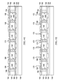
- FIGS. 49A and 49B are example package-on-package (PoP) structures according to embodiments.
- FIG. 50 is a step to form electrical connectors on the PoP structure of FIG. 49A according to an embodiment
- FIG. 51 is another example PoP structure according to an embodiment
- FIG. 52 a step to form electrical connectors on the PoP structure of FIG. 51 according to an embodiment
- FIG. 53 is a step to test the PoP structure of FIG. 50 according to an embodiment
- FIG. 54 is a step to test the PoP structure of FIG. 52 according to an embodiment.
- FIGS. 55A and 55B are further examples of PoP structures according to embodiments.
- PoP package-on-package
- FIG. 1 shows a first die 10 on a first carrier substrate 12 .
- a back side of the first die 10 is attached to the first carrier substrate 12 by an adhesive 14 .
- a front side, or active side, of the first die 10 has conductive features 16 which are electrically coupled to active devices in the first die 10 .
- the conductive features 16 are conductive pillars, such as copper, the like, or a combination thereof.
- the conductive features 16 may be any structure upon which a metallization layer may be electrically coupled, as discussed later in more detail.
- the first die 10 can be a logic circuitry die, a memory die, or any other die.
- the first carrier substrate 12 provides temporary mechanical and structural support during subsequent processing steps.
- the first carrier substrate 12 may comprise, for example, glass, silicon oxide, aluminum oxide, a combination thereof, and/or the like and may be a wafer.
- the adhesive 14 may be any suitable adhesive, such as ultraviolet (UV) glue, which loses its adhesive property when exposed to UV lights. It should be noted that multiple dies can be attached to the first carrier substrate 12 .
- FIG. 2 shows a core material, such as molding compound 18 , applied and cured over the first die 10 and the first carrier substrate 12 .
- the molding compound 18 can be an epoxy, polyimide, silicone rubber, the like, or a combination thereof.
- the molding compound 18 can be applied using acceptable techniques, such as compression molding.
- the molding compound 18 is ground and/or polished to expose the conductive features 16 on the first die 10 .
- the grinding and/or polishing may be performed using a chemical mechanical polishing (CMP) process.
- CMP chemical mechanical polishing
- FIG. 4 illustrates a front side interlayer dielectric (ILD) and redistribution layer (RDL) structure.
- a seed layer such as a copper, titanium, or the like, is deposited on the molding compound 18 , such as by sputtering or another physical vapor deposition (PVD) process.
- PVD physical vapor deposition
- a photo resist is deposited on the seed layer and patterned to expose portions of the seed layer by photolithography. The pattern is for a first metallization layer on the front side.
- Conductive material of the first metallization layer such as copper, aluminum, the like, or a combination thereof, is deposited on the exposed seed layer, such as by electroless plating, electroplating, or the like.
- the photoresist is removed by an ash and/or flush process.
- the exposed seed layer removed, such as by a wet or dry etch.
- the remaining conductive material forms the first front side metallization layer 20 , portions of which are electrically coupled to the conductive features 16
- a first ILD layer 22 is deposited on the front side and over the first metallization layer 20 .
- the first ILD layer 22 may be a polyimide, polybenzoxazole (PBO), benzocyclobutene (BCB), the like, or a combination thereof.
- the first ILD layer 22 can be deposited by a coating process, a lamination process, the like, or a combination thereof. Openings may be formed through the first ILD layer 22 to the first metallization layer 20 using acceptable photolithography techniques.
- Subsequent metallization layers and ILD layers may be formed using the same or similar processes as discussed with regard to the first metallization layer 20 and the first ILD layer 22 .
- Conductive material deposited during the formation of a subsequent metallization layer may be deposited in openings of the previously formed ILD layer to electrically couple respective metallization layers.
- the second ILD layer 26 in this embodiment, openings 28 and 30 are formed through the topmost front side ILD layer for connectors coupled between the topmost front side metallization layer, such as the second metallization layer 24 , and another package, another die, and/or another substrate. It should be noted that any number of metallization layers and ILD layers may be formed, and the use of two in this embodiment is used as an example.
- FIG. 5 shows the de-bonding of the backside of the intermediate structure from the first carrier substrate 12 and bonding the front side of the intermediate structure to a second carrier substrate 32 .
- the de-bonding from the first carrier substrate 12 may comprise exposing the adhesive 14 to UV lights, such as a laser, or by exposing the adhesive 14 to a solvent.
- the front side is bonded by an adhesive 34 .
- the second carrier substrate 32 may comprise, for example, glass, silicon oxide, aluminum oxide, a combination thereof, and/or the like and may be a wafer.
- the adhesive 34 may be any suitable adhesive, such as UV glue, which loses its adhesive property when exposed to UV lights.
- FIG. 6 illustrates a through molding via (TMV) opening formation.
- TMV openings 36 are formed through the molding compound 18 to the first front side metallization layer 20 by, for example, a laser technique or a mechanical process like drilling.
- FIG. 7 shows the TMVs 38 being formed.
- a seed layer is deposited over the back side of the structure and into the TMV openings 36 .
- the seed layer can be copper, titanium, the like, or a combination thereof deposited by sputtering, another PVD process, or the like.
- a photoresist is deposited and patterned exposing the TMV openings 36 and any other pattern for a metallization layer that is desired, such as by acceptable photolithography techniques.
- a conductive material such as copper, aluminum, the like, or a combination thereof, is deposited on the back side by electroless plating, electroplating, or the like.
- the photoresist is removed, such as by an ash and/or flush process. Remaining exposed seed layer portions are removed, such as by a wet or dry etch. TMVs 38 remain along with any further metallization pattern.
- FIG. 8 illustrates a back side ILD and RDL structure.
- FIG. 8 shows first back side ILD layer 40 , a second back side metallization layer 42 , a second ILD layer 44 , and openings 46 and 48 through the second ILD layer 44 to the second back side metallization layer 42 .
- These may be formed the similar to or in the same manner as the ILD layers and metallization layers on the front side, and therefore, explicit description of the formation of these features is omitted for brevity. Any number of metallization and ILD layers may be formed on the back side.
- FIGS. 9 through 17 illustrate a first example method for processing at a package level.
- FIG. 9 illustrates a probing step to test the first die 10 and the interconnects formed by the metallization layers and ILD layers on the front side and the back side.
- the second back side metallization layer 42 is probed by pins 50 of a probe card through the openings 46 and 48 .
- the structure is de-bonded from the second carrier substrate 32 , such as by exposing the adhesive 34 to UV lights, such as a laser, or by exposing the adhesive 34 to a solvent. Further, individual packages are singulated, such as by sawing. Known good packages, such as determined by the probing in FIG. 9 , may subsequently be used during processing.
- a second die 52 such as a memory die having a thickness of less than or equal to 3 mils, is attached through the opening 46 to conductive features in the second back side metallization layer 42 , such as by conductive connectors 54 , like controlled collapse chip connection (C 4 ) bumps.
- the second die 52 may be attached using an acceptable pick-and-place tool and reflowing connectors 54 between the second die 52 and the conductive features in the second back side metallization layer 42 .
- the connectors 54 may be a bump on trace (BOT).
- BOT bump on trace
- an underfill material 56 such as liquid epoxy, deformable gel, silicon rubber, the like, or a combination thereof, is dispensed and cured between the second die 52 and the back side of the package, such as between the second die 52 and the second metallization layer 42 .
- FIG. 13 shows the formation of conductive connectors 58 , such as ball grid array (BGA) balls, on the front side of the package in the openings 28 .
- Bond pads may be formed in the openings 28 on the front side of the package, and connectors 58 may be formed on the bond pads.
- the connectors 58 may be a lead-free solder.
- the connectors 58 are probed by pins 60 of a probe card to test the structure. Known good packages can be used in further processing.
- FIG. 15 shows a third die 62 , such as a memory die having a thickness of less than or equal to 3 mils, attached through the opening 30 to conductive features in the second front side metallization layer 24 .
- the third die 62 may be attached using an acceptable pick-and-place tool and reflowing connectors 64 , such as C 4 bumps, between the third die 62 and the conductive features in the second front side metallization layer 24 . Accordingly, the connectors 64 may be a BOT.
- the third die 62 also has a thermal interface material 66 on a back side of the third die 62 . The thermal interface material 66 may be coated on the back side of the third die 62 before the third die 62 was singulated from the wafer in which it was processed.
- the thermal interface material 66 may be an epoxy, rubber, metal (such as silver or gold), the like, or a combination thereof.
- an underfill material 68 such as liquid epoxy, deformable gel, silicon rubber, the like, or a combination thereof, is dispensed and cured between the third die 62 and the front side of the package, such as between the third die 62 and the second metallization layer 24 .
- the connectors 58 are probed using pins 70 of a probe card to test the structure. Known good packages can be used in further processing.
- FIGS. 18 through 24 illustrate a second example method for processing at a package level. Many of the components in FIGS. 18 through 24 are the same as or similar to components discussed with respect to FIGS. 11 through 17 . A person having ordinary skill in the art will readily understand these similarities, and therefore, some explicit discussion of these components is omitted for brevity.
- FIG. 18 shows a second die 80 , such as a memory die having a thickness of less than or equal to 3 mils, attached through the opening 30 to conductive features in the second front side metallization layer 24 by conductive connectors 82 , such as C 4 bumps.
- a second die 80 such as a memory die having a thickness of less than or equal to 3 mils
- conductive connectors 82 such as C 4 bumps.
- an underfill material 84 is dispensed and cured between the second die 80 and the front side of the package, such as between the second die 80 and the second metallization layer 24 .
- FIG. 20 shows the formation of conductive connectors 86 , such as BGA balls, on the back side of the package. Bond pads may be formed in the openings 48 on the back side of the package, and connectors 86 may be formed on the bond pads.
- the connectors 86 are probed by pins 88 of a probe card to test the structure. Known good packages can be used in further processing.
- FIG. 22 shows a third die 90 , such as a memory die having a thickness of less than or equal to 3 mils, with a thermal interface material 94 on a back side, and the third die 90 is attached through the opening 46 to conductive features in the second back side metallization layer 42 by conductive connectors 92 , such as C 4 bumps.
- conductive connectors 92 such as C 4 bumps.
- an underfill material 96 is dispensed and cured between the third die 90 and the back side of the package, such as between the third die 90 and the second metallization layer 42 .
- the connectors 86 are probed by pins 98 of a probe card to test the structure. Known good packages can be used in further processing.
- FIGS. 25 through 33 illustrate an example method for processing at a wafer level.
- many of the components in FIGS. 25 through 33 are the same as or similar to components discussed with respect to previous figures. A person having ordinary skill in the art will readily understand these similarities, and therefore, some explicit discussion of these components is omitted for brevity.
- the conductive connectors 110 are formed in openings 48 on the back side of the package, as shown in FIG. 25 .
- Bond pads may be formed in the openings 48 on the back side of the package, and connectors 110 may be formed on the bond pads.
- the connectors may be a lead-free solder.
- the connectors 110 are probed by pins 112 of a probe card to test the structure. Known good packages can be used in further processing.
- a second die 114 such as a memory die having a thickness of less than or equal to 3 mils, with a thermal interface material 118 on a back side is attached through the opening 46 to conductive features in the second back side metallization layer 42 by conductive connectors 116 , such as C 4 bumps.
- conductive connectors 116 such as C 4 bumps.
- an underfill material 120 is dispensed and cured between the second die 114 and the back side of the package, such as between the second die 114 and the second metallization layer 42 .
- the connectors 110 are probed by pins 122 of a probe card to test the structure. Known good packages can be used in further processing.
- FIG. 30 the structure is de-bonded from the second carrier substrate 32 , and individual packages are singulated.
- FIG. 31 shows a third die 124 , such as a memory die having a thickness of less than or equal to 3 mils, attached through the opening 30 to conductive features in the second front side metallization layer 24 by conductive connectors 126 , such as C 4 bumps.
- a third die 124 such as a memory die having a thickness of less than or equal to 3 mils
- conductive connectors 126 such as C 4 bumps.
- an underfill material 128 is dispensed and cured between the third die 124 and the front side of the package, such as between the third die 124 and the second front side metallization layer 24 .
- the connectors 110 are probed by pins 130 of a probe card to test the structure. Known good packages can be used in further processing.
- FIGS. 34 through 48 illustrate a method of forming an interposer and a die attached to the interposer.
- a substrate 140 of an interposer is shown with through substrate via (TSV) recesses 142 formed through a front side of the substrate 140 .
- the substrate 140 generally comprises a material similar to the substrate used to form a die that will be attached to the interposer, such as silicon. While the substrate 140 may be formed of other materials, it is believed that using silicon substrates for the interposer may reduce stress because the coefficient of thermal expansion (CTE) mismatch between the silicon substrates and the silicon typically used for the dies is lower than with substrates formed of different materials.
- the TSV recesses 142 are formed by, for example, etching, milling, laser techniques, a combination thereof, and/or the like.
- FIG. 35 shows the formation of an isolation layer 144 over the front surface of the substrate 140 and in the recesses 142 .
- the isolation layer 144 can be, for example, silicon oxide, silicon nitride, the like, or a combination thereof.
- the isolation layer 144 can be formed by, for example, a chemical vapor deposition (CVD) process, a thermal oxidation process, an atomic layer deposition process (ALD), the like, or a combination thereof.
- CVD chemical vapor deposition
- ALD atomic layer deposition
- FIG. 36 shows the deposition of a conductive material 146 .
- a seed layer is deposited over the front surface of the substrate 140 and in the recesses 142 .
- the seed layer can be copper, titanium, the like, or a combination thereof, and can be deposited by sputtering, another PVD process, the like, or a combination thereof.
- the conductive material 146 such as copper, aluminum, tungsten, silver, gold, the like or a combination thereof, is deposited over the seed layer using, for example, electroplating, electroless plating, the like, or a combination thereof.
- excess conductive material 146 and isolation layer 144 is removed from the front side of the substrate 140 by, for example, (CMP).
- CMP CMP
- the TSVs 148 comprise a conductive material and an isolation layer between the conductive material and the substrate 140 .
- Front side processing continues in FIG. 38 with the formation of a front side RDL.
- the RDL may comprise any number or combination of metallization layers, ILD layers, vias, and passivation layers.
- the RDL depicted in FIG. 38 comprises one front side metallization layer 152 and two ILD layers 150 and 154 .
- a first ILD layer 150 is deposited on the front side of the substrate 140 .
- the first ILD layer 150 may be a polyimide, PBO, BCB, silicon oxide, the like, or a combination thereof.
- the first ILD layer 150 can be deposited by a coating process, a lamination process, a CVD process, the like, or a combination thereof.
- Openings may be formed through the first ILD layer 150 to the TSVs 148 using acceptable photolithography techniques and/or etching.
- a seed layer such as a copper, titanium, or the like, is deposited on the first ILD layer 150 and in the openings to the TSVs 148 , such as by sputtering or another physical vapor deposition (PVD) process.
- PVD physical vapor deposition
- a photo resist is deposited on the seed layer and patterned to expose portions of the seed layer by photolithography. The pattern is of a first metallization layer on the front side.
- Conductive material of the first metallization layer 152 is deposited on the exposed seed layer, such as by electroless plating, electroplating, or the like.
- the photoresist is removed by an ash and/or flush process.
- the exposed seed layer removed, such as by a wet or dry etch.
- the remaining conductive material forms the first front side metallization layer 152 , portions of which are electrically coupled to the TSVs 148 .
- a second ILD layer 154 is deposited on the first ILD layer 150 and over the first metallization layer 152 .
- the second ILD layer 154 may be a polyimide, PBO, BCB, silicon oxide, the like, or a combination thereof.
- the second ILD layer 154 can be deposited by a coating process, a lamination process, a CVD process, the like, or a combination thereof. Openings 156 may be formed through the second ILD layer 154 to the first metallization layer 152 using acceptable photolithography techniques and/or etching techniques.
- the front side of the structure in FIG. 38 is then attached to a carrier substrate 158 by an adhesive 160 .
- the carrier substrate 158 may comprise, for example, glass, silicon oxide, aluminum oxide, a combination thereof, and/or the like.
- the adhesive 160 may be any suitable adhesive, such as UV glue.
- Back side processing begins as shown in FIG. 40 .
- the back side of the substrate 140 is ground and/or polished, such as by CMP, and/or etched to expose the TSVs 148 on the back side of the substrate 140 by thinning the substrate 140 .
- a first ILD layer 162 , a metallization layer 164 , and a second ILD layer 166 are formed the same as or similar to corresponding components discussed with respect to the front side of the substrate 140 in FIG. 38 . Any number of ILD layer and metallization layers may be formed. Openings 168 and 170 are formed through the second ILD layer 166 using acceptable photolithography techniques and/or etching techniques.
- the metallization layer 164 on the back side is probed by pins 172 of a probe card through the openings 168 and 170 for testing.
- Known good interposers can be used for further processing.
- a die 174 such as a logic circuitry die, is attached through the opening 170 by the conductive connectors 176 , such as C 4 bumps.
- the die 174 may be known good dies attached using a pick-and-place tool, and the conductive connectors 176 may be reflowed.
- the connectors 176 are attached to conductive features in the back side metallization layer 164 , and thus, the die 174 uses BOT technology.
- an underfill material 178 is dispensed and cured between the die 174 and the interposer, for example, the back side metallization layer 164 .
- the underfill material 178 may be a liquid epoxy, deformable gel, silicon rubber, a combination thereof, and/or the like dispensed using acceptable dispensing equipment.
- the back side metallization layer 164 is probed through openings 168 by pins 180 of a probe card for testing. Known good dies and interposers can be used for further processing.
- FIG. 46 shows the de-bonding of the front side of the interposer from the carrier substrate 158 and singluation of individual interposers.
- the de-bonding from the carrier substrate 158 may comprise exposing the adhesive 160 to UV lights, such as a laser, or by exposing the adhesive 160 to a solvent.
- FIG. 47 illustrates the formation of conductive connectors 182 , such as BGA balls, on the front side of the interposer. Bond pads may be formed in the openings 156 on the front side of the interposer, and connectors 182 may be formed on the bond pads.
- the connectors may be a lead-free solder.
- the connectors 182 are probed by pins 184 of a probe card to test the structure. Known good interposers and dies can be used in further processing.
- packages are stacked to form the PoP structure.
- a package 202 comprising a first die encased in molding compound, a second die on a back side of the package, and a third die on a front side of the package is stacked on an interposer package 204 comprising a die on a top surface of an interposer.
- the package 202 can be the package formed in FIG. 17
- the interposer package 204 can be the package formed in FIG. 48 .
- FIG. 49A a package 202 comprising a first die encased in molding compound, a second die on a back side of the package, and a third die on a front side of the package is stacked on an interposer package 204 comprising a die on a top surface of an interposer.
- the package 202 can be the package formed in FIG. 17
- the interposer package 204 can be the package formed in FIG. 48 .
- a package 206 comprising a first die encased in molding compound, a second die on a front side of the package, and a third die on a back side of the package is stacked on an interposer package 204 comprising a die on a top surface of an interposer.
- the package 202 can be the package formed in FIGS. 24 and 33
- the interposer package 204 can be the package formed in FIG. 48 .
- the package 202 and 206 respectively, is attached to the interposer package 204 with conductive connectors, such as BGA balls, coupling a metallization layer on a back side of the interposer. The conductive connectors are then reflowed to more permanently attach the packages.
- the PoP structure of FIG. 49A for example, has conductive connectors 208 , such as BGA balls, formed coupled to a metallization layer on a front side of the interposer of the interposer package 204 .
- the connectors 208 may be formed before the packages 202 and 204 are stacked, such as described in FIG. 13 , or after the packages 202 and 204 are stacked, as shown in FIG. 50 .
- the PoP structure of 49 B can similarly have conductive connectors formed, although not explicitly depicted.
- FIG. 51 shows that multiple packages 202 (or packages 206 ) can be stacked in the PoP structure.
- connectors 210 such as BGA balls, formed coupled to a metallization layer on a front side of the interposer of the interposer package 204 , similar to FIG. 50 .
- the PoP structures of FIGS. 50 and 52 have connectors 208 and 210 probed by pins 212 and 214 of a probe card for testing the PoP structures, respectively.
- Embodiments may achieve a more efficient use of space by placing a die within a substrate of a package. By placing the die within the substrate of a package, another substrate may not be required to have the die on a surface.
- An embodiment is a package-on-package (PoP) structure.
- the structure comprises a first package and a second package.
- the first package comprises a first die, a second die, and a first core material.
- the first core material has a first surface and a second surface opposite the first surface.
- a first redistribution layer (RDL) is on the first surface of the first core material, and a second RDL is on the second surface of the first core material.
- the first die is disposed in the first core material between the first surface of the first core material and the second surface of the first core material.
- the second die is coupled to one of the first RDL and the second RDL.
- the second package comprises a third die and an interposer.
- the interposer has a first side and a second side opposite the first side.
- the third die is coupled to the second side of the interposer.
- the first package is coupled to the second package by first electrical connectors coupled to the second side of the interposer and the first R
- the structure comprises an interposer, a first die, a first substrate comprising a second die, and a third die.
- the interposer has a first side and a second side opposite the first side.
- the first die is on the second side of the interposer.
- the first substrate is on and coupled to the second side of the interposer by first electrical connectors.
- the first substrate comprises a first core material, a first RDL, the second die, and a second RDL.
- the first core material has a first surface and a second surface.
- the first RDL is on the first surface of the first core material, and the first RDL is coupled to the first electrical connectors.
- the second die is disposed in the first core material between the first surface of the first core material and the second surface of the first core material.
- the second RDL is on the second surface of the first core material.
- the third die is on the first substrate.
- a further embodiment is a method for forming a PoP structure.
- the method comprises applying a first molding compound on a first die, first electrical connectors electrically coupled to the first die being exposed through a first surface of the first molding compound; forming a first redistribution layer (RDL) on the first surface of the first molding compound, the first RDL on the first molding compound being electrically coupled to the first electrical connectors; forming a second RDL on a second surface of the first molding compound; attaching a second die to one of the first RDL on the first molding compound and the second RDL on the first molding compound; and attaching second electrical connectors to one of the first RDL on the first molding compound and the second RDL on the first molding compound and to a first side of an interposer, the interposer having a third die on the first side of the interposer
- FIGS. 55A and 55B show examples.
- the modified packages 202 ′ and 206 ′ comprise one less die that the packages 202 and 206 in FIGS. 49A and 49B , respectively.
- a person having ordinary skill in the art will readily understand how to achieve this PoP structure based on this disclosure, and thus, further explicit description is omitted for brevity.
Landscapes
- Production Of Multi-Layered Print Wiring Board (AREA)
- Engineering & Computer Science (AREA)
- Manufacturing & Machinery (AREA)
Abstract
Description
Claims (13)
Priority Applications (2)
| Application Number | Priority Date | Filing Date | Title |
|---|---|---|---|
| US13/271,952 US9123763B2 (en) | 2011-10-12 | 2011-10-12 | Package-on-package (PoP) structure having at least one package comprising one die being disposed in a core material between first and second surfaces of the core material |
| US14/828,244 US9418978B2 (en) | 2011-10-12 | 2015-08-17 | Method of forming package-on-package (PoP) structure having a chip package with a plurality of dies attaching to first side of an interposer with a die formed thereon |
Applications Claiming Priority (1)
| Application Number | Priority Date | Filing Date | Title |
|---|---|---|---|
| US13/271,952 US9123763B2 (en) | 2011-10-12 | 2011-10-12 | Package-on-package (PoP) structure having at least one package comprising one die being disposed in a core material between first and second surfaces of the core material |
Related Child Applications (1)
| Application Number | Title | Priority Date | Filing Date |
|---|---|---|---|
| US14/828,244 Division US9418978B2 (en) | 2011-10-12 | 2015-08-17 | Method of forming package-on-package (PoP) structure having a chip package with a plurality of dies attaching to first side of an interposer with a die formed thereon |
Publications (2)
| Publication Number | Publication Date |
|---|---|
| US20130093097A1 US20130093097A1 (en) | 2013-04-18 |
| US9123763B2 true US9123763B2 (en) | 2015-09-01 |
Family
ID=48085451
Family Applications (2)
| Application Number | Title | Priority Date | Filing Date |
|---|---|---|---|
| US13/271,952 Active 2032-01-07 US9123763B2 (en) | 2011-10-12 | 2011-10-12 | Package-on-package (PoP) structure having at least one package comprising one die being disposed in a core material between first and second surfaces of the core material |
| US14/828,244 Active US9418978B2 (en) | 2011-10-12 | 2015-08-17 | Method of forming package-on-package (PoP) structure having a chip package with a plurality of dies attaching to first side of an interposer with a die formed thereon |
Family Applications After (1)
| Application Number | Title | Priority Date | Filing Date |
|---|---|---|---|
| US14/828,244 Active US9418978B2 (en) | 2011-10-12 | 2015-08-17 | Method of forming package-on-package (PoP) structure having a chip package with a plurality of dies attaching to first side of an interposer with a die formed thereon |
Country Status (1)
| Country | Link |
|---|---|
| US (2) | US9123763B2 (en) |
Cited By (7)
| Publication number | Priority date | Publication date | Assignee | Title |
|---|---|---|---|---|
| US20160013147A1 (en) * | 2014-07-08 | 2016-01-14 | Taiwan Semiconductor Manufacturing Company, Ltd. | Methods for forming fan-out package structure |
| US9607967B1 (en) * | 2015-11-04 | 2017-03-28 | Inotera Memories, Inc. | Multi-chip semiconductor package with via components and method for manufacturing the same |
| US10186500B2 (en) | 2015-12-10 | 2019-01-22 | Samsung Electronics Co., Ltd. | Semiconductor package and method of fabricating the same |
| US20190067181A1 (en) * | 2017-02-16 | 2019-02-28 | Advanced Semiconductor Engineering, Inc. | Semiconductor packages |
| US20220068866A1 (en) * | 2020-09-03 | 2022-03-03 | Stmicroelectronics (Tours) Sas | Die with metal pillars |
| US11342316B2 (en) | 2020-01-16 | 2022-05-24 | Mediatek Inc. | Semiconductor package |
| US20230034737A1 (en) * | 2021-07-30 | 2023-02-02 | Intel Corporation | Composite ic die package including ic die directly bonded to front and back sides of an interposer |
Families Citing this family (51)
| Publication number | Priority date | Publication date | Assignee | Title |
|---|---|---|---|---|
| WO2011044289A1 (en) * | 2009-10-07 | 2011-04-14 | Rain Bird Corporation | Volumetric budget based irrigation control |
| US9385095B2 (en) | 2010-02-26 | 2016-07-05 | Taiwan Semiconductor Manufacturing Company, Ltd. | 3D semiconductor package interposer with die cavity |
| US9123763B2 (en) | 2011-10-12 | 2015-09-01 | Taiwan Semiconductor Manufacturing Company, Ltd. | Package-on-package (PoP) structure having at least one package comprising one die being disposed in a core material between first and second surfaces of the core material |
| US8975741B2 (en) | 2011-10-17 | 2015-03-10 | Taiwan Semiconductor Manufacturing Company, Ltd. | Process for forming package-on-package structures |
| US9484319B2 (en) * | 2011-12-23 | 2016-11-01 | STATS ChipPAC Pte. Ltd. | Semiconductor device and method of forming extended semiconductor device with fan-out interconnect structure to reduce complexity of substrate |
| KR101332916B1 (en) * | 2011-12-29 | 2013-11-26 | 주식회사 네패스 | Semiconductor package and method of manufacturing the same |
| US8872326B2 (en) | 2012-08-29 | 2014-10-28 | Taiwan Semiconductor Manufacturing Company, Ltd. | Three dimensional (3D) fan-out packaging mechanisms |
| KR20140086531A (en) * | 2012-12-28 | 2014-07-08 | 삼성전기주식회사 | Package structure and manufacturing method thereof, and package on package substrate |
| US8884427B2 (en) | 2013-03-14 | 2014-11-11 | Invensas Corporation | Low CTE interposer without TSV structure |
| KR101488608B1 (en) | 2013-07-19 | 2015-02-02 | 앰코 테크놀로지 코리아 주식회사 | Semiconductor device and manufacturing method thereof |
| GB201313850D0 (en) * | 2013-08-02 | 2013-09-18 | Johnson Matthey Plc | Getter composition |
| US9870946B2 (en) | 2013-12-31 | 2018-01-16 | Taiwan Semiconductor Manufacturing Company, Ltd. | Wafer level package structure and method of forming same |
| US10056267B2 (en) | 2014-02-14 | 2018-08-21 | Taiwan Semiconductor Manufacturing Company, Ltd. | Substrate design for semiconductor packages and method of forming same |
| US9653443B2 (en) | 2014-02-14 | 2017-05-16 | Taiwan Semiconductor Manufacturing Company, Ltd. | Thermal performance structure for semiconductor packages and method of forming same |
| US10026671B2 (en) * | 2014-02-14 | 2018-07-17 | Taiwan Semiconductor Manufacturing Company, Ltd. | Substrate design for semiconductor packages and method of forming same |
| US9904814B2 (en) * | 2014-03-18 | 2018-02-27 | Hewlett-Packard Development Company, L.P. | Secure element |
| JP6356450B2 (en) * | 2014-03-20 | 2018-07-11 | 株式会社東芝 | Semiconductor device and electronic circuit device |
| US9589924B2 (en) * | 2014-08-28 | 2017-03-07 | Taiwan Semiconductor Manufacturing Company Ltd. | Semiconductor structure and method of manufacturing the same |
| US9972601B2 (en) | 2014-09-26 | 2018-05-15 | Intel Corporation | Integrated circuit package having wirebonded multi-die stack |
| TWI548050B (en) * | 2014-11-03 | 2016-09-01 | 矽品精密工業股份有限公司 | Package structure and its manufacturing method and package substrate |
| US10325853B2 (en) * | 2014-12-03 | 2019-06-18 | Taiwan Semiconductor Manufacturing Company, Ltd. | Method of forming semiconductor packages having through package vias |
| KR20160122020A (en) * | 2015-04-13 | 2016-10-21 | 에스케이하이닉스 주식회사 | Substrate, semiconductor package including the same |
| US10276541B2 (en) * | 2015-06-30 | 2019-04-30 | Taiwan Semiconductor Manufacturing Company, Ltd. | 3D package structure and methods of forming same |
| US12550783B2 (en) * | 2016-05-17 | 2026-02-10 | Taiwan Semiconductor Manufacturing Company, Ltd. | Device and method for UBM/RDL routing |
| US9818729B1 (en) * | 2016-06-16 | 2017-11-14 | Taiwan Semiconductor Manufacturing Company, Ltd. | Package-on-package structure and method |
| US9991164B2 (en) | 2016-06-22 | 2018-06-05 | Semiconductor Components Industries, Llc | Semiconductor die singulation methods |
| US11075118B2 (en) | 2016-06-22 | 2021-07-27 | Semiconductor Components Industries, Llc | Semiconductor die singulation methods |
| US10403544B2 (en) | 2016-06-22 | 2019-09-03 | Semiconductor Components Industries, Llc | Semiconductor die singulation methods |
| US10541226B2 (en) * | 2016-07-29 | 2020-01-21 | Taiwan Semiconductor Manufacturing Co., Ltd. | Package structure and method of forming the same |
| US10700035B2 (en) * | 2016-11-04 | 2020-06-30 | General Electric Company | Stacked electronics package and method of manufacturing thereof |
| US10312194B2 (en) | 2016-11-04 | 2019-06-04 | General Electric Company | Stacked electronics package and method of manufacturing thereof |
| US20180130731A1 (en) * | 2016-11-04 | 2018-05-10 | General Electric Company | Electronics package having a multi-thickness conductor layer and method of manufacturing thereof |
| US9966371B1 (en) | 2016-11-04 | 2018-05-08 | General Electric Company | Electronics package having a multi-thickness conductor layer and method of manufacturing thereof |
| US9966361B1 (en) | 2016-11-04 | 2018-05-08 | General Electric Company | Electronics package having a multi-thickness conductor layer and method of manufacturing thereof |
| DE102017127920A1 (en) | 2017-01-26 | 2018-07-26 | Taiwan Semiconductor Manufacturing Company, Ltd. | Increased through-hole for connections on different levels |
| US9972581B1 (en) * | 2017-02-07 | 2018-05-15 | Taiwan Semiconductor Manufacturing Company, Ltd. | Routing design of dummy metal cap and redistribution line |
| WO2018182598A1 (en) * | 2017-03-29 | 2018-10-04 | Intel Corporation | Side mounted interconnect bridges |
| US10181447B2 (en) | 2017-04-21 | 2019-01-15 | Invensas Corporation | 3D-interconnect |
| TWI656611B (en) * | 2017-12-28 | 2019-04-11 | 黃斐琪 | Flip-chip package structure of power chip and the packaging method thereof |
| US10622302B2 (en) | 2018-02-14 | 2020-04-14 | Taiwan Semiconductor Manufacturing Company, Ltd. | Via for semiconductor device connection and methods of forming the same |
| US10497648B2 (en) | 2018-04-03 | 2019-12-03 | General Electric Company | Embedded electronics package with multi-thickness interconnect structure and method of making same |
| US10515920B2 (en) * | 2018-04-09 | 2019-12-24 | Google Llc | High bandwidth memory package for high performance processors |
| US11158775B2 (en) | 2018-06-08 | 2021-10-26 | Taiwan Semiconductor Manufacturing Company, Ltd. | Semiconductor device and method |
| DE102018126130B4 (en) | 2018-06-08 | 2023-08-10 | Taiwan Semiconductor Manufacturing Co., Ltd. | semiconductor device and method |
| US10992100B2 (en) | 2018-07-06 | 2021-04-27 | Taiwan Semiconductor Manufacturing Company, Ltd. | Semiconductor device and method |
| US11728278B2 (en) * | 2019-03-25 | 2023-08-15 | Taiwan Semiconductor Manufacturing Company, Ltd. | Board substrates, three-dimensional integrated circuit structures and methods of forming the same |
| CN111799182A (en) * | 2019-04-09 | 2020-10-20 | 矽品精密工业股份有限公司 | Package stack structure and its manufacturing method |
| CN113990759B (en) * | 2020-12-21 | 2025-07-22 | 矽磐微电子(重庆)有限公司 | Semiconductor packaging method and semiconductor packaging structure |
| US12040284B2 (en) | 2021-11-12 | 2024-07-16 | Invensas Llc | 3D-interconnect with electromagnetic interference (“EMI”) shield and/or antenna |
| US12199007B2 (en) | 2022-03-11 | 2025-01-14 | Broadcom International Pte. Ltd. | Copper connected glass modules on a glass board |
| US20250046622A1 (en) * | 2023-08-04 | 2025-02-06 | Avago Technologies International Sales Pte. Limited | Hybrid substrates and manufacturing methods thereof |
Citations (15)
| Publication number | Priority date | Publication date | Assignee | Title |
|---|---|---|---|---|
| US5241456A (en) * | 1990-07-02 | 1993-08-31 | General Electric Company | Compact high density interconnect structure |
| US6960827B2 (en) * | 2002-04-19 | 2005-11-01 | Fujitsu Limited | Semiconductor device and manufacturing method thereof |
| US20060170098A1 (en) * | 2005-02-01 | 2006-08-03 | Shih-Ping Hsu | Module structure having embedded chips |
| US7226808B2 (en) * | 2003-05-02 | 2007-06-05 | Seiko Epson Corporation | Method of manufacturing semiconductor device and method of manufacturing electronics device |
| US7230329B2 (en) * | 2003-02-07 | 2007-06-12 | Seiko Epson Corporation | Semiconductor device, electronic device, electronic equipment, method of manufacturing semiconductor device, and method of manufacturing electronic device |
| US7321164B2 (en) * | 2005-08-15 | 2008-01-22 | Phoenix Precision Technology Corporation | Stack structure with semiconductor chip embedded in carrier |
| US20080136004A1 (en) * | 2006-12-08 | 2008-06-12 | Advanced Chip Engineering Technology Inc. | Multi-chip package structure and method of forming the same |
| US20090039491A1 (en) * | 2007-08-10 | 2009-02-12 | Samsung Electronics Co., Ltd. | Semiconductor package having buried post in encapsulant and method of manufacturing the same |
| US7498666B2 (en) * | 2004-09-27 | 2009-03-03 | Nokia Corporation | Stacked integrated circuit |
| US7573136B2 (en) * | 2002-06-27 | 2009-08-11 | Micron Technology, Inc. | Semiconductor device assemblies and packages including multiple semiconductor device components |
| US7781877B2 (en) * | 2007-08-07 | 2010-08-24 | Micron Technology, Inc. | Packaged integrated circuit devices with through-body conductive vias, and methods of making same |
| US20100252937A1 (en) * | 2009-04-06 | 2010-10-07 | Shinko Electric Industries Co., Ltd. | Electronic device and method of manufacturing same |
| US20120199972A1 (en) | 2006-11-10 | 2012-08-09 | Stats Chippac, Ltd. | Semiconductor Device and Method of Forming Vertical Interconnect Structure Using Stud Bumps |
| US20130093078A1 (en) * | 2011-10-17 | 2013-04-18 | Taiwan Semiconductor Manufacturing Company, Ltd. | Process for Forming Package-on-Package Structures |
| US8519544B2 (en) | 2011-02-22 | 2013-08-27 | STATS Chip PAC, Ltd. | Semiconductor device and method of forming WLCSP structure using protruded MLP |
Family Cites Families (7)
| Publication number | Priority date | Publication date | Assignee | Title |
|---|---|---|---|---|
| US8039303B2 (en) | 2008-06-11 | 2011-10-18 | Stats Chippac, Ltd. | Method of forming stress relief layer between die and interconnect structure |
| US8426955B2 (en) | 2009-06-12 | 2013-04-23 | Stats Chippac Ltd. | Integrated circuit packaging system with a stack package and method of manufacture thereof |
| US8039304B2 (en) | 2009-08-12 | 2011-10-18 | Stats Chippac, Ltd. | Semiconductor device and method of dual-molding die formed on opposite sides of build-up interconnect structures |
| US8749040B2 (en) | 2009-09-21 | 2014-06-10 | Stats Chippac Ltd. | Integrated circuit packaging system with package-on-package and method of manufacture thereof |
| US9054098B2 (en) | 2011-08-30 | 2015-06-09 | Stats Chippac Ltd. | Integrated circuit packaging system with redistribution layer and method of manufacture thereof |
| US9123763B2 (en) | 2011-10-12 | 2015-09-01 | Taiwan Semiconductor Manufacturing Company, Ltd. | Package-on-package (PoP) structure having at least one package comprising one die being disposed in a core material between first and second surfaces of the core material |
| US9349616B2 (en) | 2013-03-13 | 2016-05-24 | Stats Chippac, Ltd. | Semiconductor device and method of forming WLCSP with semiconductor die embedded within interconnect structure |
-
2011
- 2011-10-12 US US13/271,952 patent/US9123763B2/en active Active
-
2015
- 2015-08-17 US US14/828,244 patent/US9418978B2/en active Active
Patent Citations (17)
| Publication number | Priority date | Publication date | Assignee | Title |
|---|---|---|---|---|
| US5241456A (en) * | 1990-07-02 | 1993-08-31 | General Electric Company | Compact high density interconnect structure |
| US6960827B2 (en) * | 2002-04-19 | 2005-11-01 | Fujitsu Limited | Semiconductor device and manufacturing method thereof |
| US7573136B2 (en) * | 2002-06-27 | 2009-08-11 | Micron Technology, Inc. | Semiconductor device assemblies and packages including multiple semiconductor device components |
| US7230329B2 (en) * | 2003-02-07 | 2007-06-12 | Seiko Epson Corporation | Semiconductor device, electronic device, electronic equipment, method of manufacturing semiconductor device, and method of manufacturing electronic device |
| US7226808B2 (en) * | 2003-05-02 | 2007-06-05 | Seiko Epson Corporation | Method of manufacturing semiconductor device and method of manufacturing electronics device |
| US7498666B2 (en) * | 2004-09-27 | 2009-03-03 | Nokia Corporation | Stacked integrated circuit |
| US20060170098A1 (en) * | 2005-02-01 | 2006-08-03 | Shih-Ping Hsu | Module structure having embedded chips |
| US7321164B2 (en) * | 2005-08-15 | 2008-01-22 | Phoenix Precision Technology Corporation | Stack structure with semiconductor chip embedded in carrier |
| US20120199972A1 (en) | 2006-11-10 | 2012-08-09 | Stats Chippac, Ltd. | Semiconductor Device and Method of Forming Vertical Interconnect Structure Using Stud Bumps |
| US20080136004A1 (en) * | 2006-12-08 | 2008-06-12 | Advanced Chip Engineering Technology Inc. | Multi-chip package structure and method of forming the same |
| US7781877B2 (en) * | 2007-08-07 | 2010-08-24 | Micron Technology, Inc. | Packaged integrated circuit devices with through-body conductive vias, and methods of making same |
| US20090039491A1 (en) * | 2007-08-10 | 2009-02-12 | Samsung Electronics Co., Ltd. | Semiconductor package having buried post in encapsulant and method of manufacturing the same |
| US20100252937A1 (en) * | 2009-04-06 | 2010-10-07 | Shinko Electric Industries Co., Ltd. | Electronic device and method of manufacturing same |
| US8174109B2 (en) | 2009-04-06 | 2012-05-08 | Shinko Electric Industries Co., Ltd. | Electronic device and method of manufacturing same |
| US8519544B2 (en) | 2011-02-22 | 2013-08-27 | STATS Chip PAC, Ltd. | Semiconductor device and method of forming WLCSP structure using protruded MLP |
| US20130093078A1 (en) * | 2011-10-17 | 2013-04-18 | Taiwan Semiconductor Manufacturing Company, Ltd. | Process for Forming Package-on-Package Structures |
| US8975741B2 (en) * | 2011-10-17 | 2015-03-10 | Taiwan Semiconductor Manufacturing Company, Ltd. | Process for forming package-on-package structures |
Cited By (13)
| Publication number | Priority date | Publication date | Assignee | Title |
|---|---|---|---|---|
| US9691726B2 (en) * | 2014-07-08 | 2017-06-27 | Taiwan Semiconductor Manufacturing Company, Ltd. | Methods for forming fan-out package structure |
| US20160013147A1 (en) * | 2014-07-08 | 2016-01-14 | Taiwan Semiconductor Manufacturing Company, Ltd. | Methods for forming fan-out package structure |
| US9607967B1 (en) * | 2015-11-04 | 2017-03-28 | Inotera Memories, Inc. | Multi-chip semiconductor package with via components and method for manufacturing the same |
| US10734367B2 (en) | 2015-12-10 | 2020-08-04 | Sansumg Electronics Co., Ltd. | Semiconductor package and method of fabricating the same |
| US10186500B2 (en) | 2015-12-10 | 2019-01-22 | Samsung Electronics Co., Ltd. | Semiconductor package and method of fabricating the same |
| US10867899B2 (en) * | 2017-02-16 | 2020-12-15 | Advanced Semiconductor Engineering, Inc. | Semiconductor packages |
| US20190067181A1 (en) * | 2017-02-16 | 2019-02-28 | Advanced Semiconductor Engineering, Inc. | Semiconductor packages |
| US11342316B2 (en) | 2020-01-16 | 2022-05-24 | Mediatek Inc. | Semiconductor package |
| US11728320B2 (en) | 2020-01-16 | 2023-08-15 | Mediatek Inc. | Semiconductor package |
| US20220068866A1 (en) * | 2020-09-03 | 2022-03-03 | Stmicroelectronics (Tours) Sas | Die with metal pillars |
| US11824028B2 (en) * | 2020-09-03 | 2023-11-21 | Stmicroelectronics (Tours) Sas | Die with metal pillars |
| US12374643B2 (en) | 2020-09-03 | 2025-07-29 | Stmicroelectronics (Tours) Sas | Die with metal pillars |
| US20230034737A1 (en) * | 2021-07-30 | 2023-02-02 | Intel Corporation | Composite ic die package including ic die directly bonded to front and back sides of an interposer |
Also Published As
| Publication number | Publication date |
|---|---|
| US9418978B2 (en) | 2016-08-16 |
| US20150357320A1 (en) | 2015-12-10 |
| US20130093097A1 (en) | 2013-04-18 |
Similar Documents
| Publication | Publication Date | Title |
|---|---|---|
| US9418978B2 (en) | Method of forming package-on-package (PoP) structure having a chip package with a plurality of dies attaching to first side of an interposer with a die formed thereon | |
| US11476125B2 (en) | Multi-die package with bridge layer | |
| US11984372B2 (en) | Integrated circuit package and method | |
| US12087757B2 (en) | Integrated circuit packages | |
| US11854921B2 (en) | Integrated circuit package and method | |
| TWI670778B (en) | Package structures and methods of forming the same | |
| TWI773260B (en) | Package structure and method for forming the same | |
| KR102455197B1 (en) | Integrated circuit package and method | |
| US9748216B2 (en) | Apparatus and method for a component package | |
| TW201916304A (en) | Semiconductor package | |
| US20140210080A1 (en) | PoP Device | |
| US12211707B2 (en) | Integrated circuit package and method of forming thereof | |
| US9548283B2 (en) | Package redistribution layer structure and method of forming same | |
| US20250183213A1 (en) | Semiconductor structure and forming method thereof | |
| TWI896033B (en) | Semiconductor package structures and methods of forming same | |
| US20250385157A1 (en) | Semiconductor packages and methods of forming same | |
| US12588549B2 (en) | Integrated circuit package and method | |
| KR102473590B1 (en) | Semiconductor device and method | |
| US20250343170A1 (en) | Package connectors in semiconductor packages and methods of forming |
Legal Events
| Date | Code | Title | Description |
|---|---|---|---|
| AS | Assignment |
Owner name: TAIWAN SEMICONDUCTOR MANUFACTURING COMPANY, LTD., Free format text: ASSIGNMENT OF ASSIGNORS INTEREST;ASSIGNORS:YU, CHEN-HUA;LIU, CHUNG-SHI;LII, MIRNG-JI;AND OTHERS;SIGNING DATES FROM 20111005 TO 20111006;REEL/FRAME:027325/0763 |
|
| STCF | Information on status: patent grant |
Free format text: PATENTED CASE |
|
| MAFP | Maintenance fee payment |
Free format text: PAYMENT OF MAINTENANCE FEE, 4TH YEAR, LARGE ENTITY (ORIGINAL EVENT CODE: M1551); ENTITY STATUS OF PATENT OWNER: LARGE ENTITY Year of fee payment: 4 |
|
| MAFP | Maintenance fee payment |
Free format text: PAYMENT OF MAINTENANCE FEE, 8TH YEAR, LARGE ENTITY (ORIGINAL EVENT CODE: M1552); ENTITY STATUS OF PATENT OWNER: LARGE ENTITY Year of fee payment: 8 |