US9117040B2 - Induced field determination using diffuse field reciprocity - Google Patents
Induced field determination using diffuse field reciprocity Download PDFInfo
- Publication number
- US9117040B2 US9117040B2 US13/227,330 US201113227330A US9117040B2 US 9117040 B2 US9117040 B2 US 9117040B2 US 201113227330 A US201113227330 A US 201113227330A US 9117040 B2 US9117040 B2 US 9117040B2
- Authority
- US
- United States
- Prior art keywords
- metric
- conductive element
- executing
- computer instructions
- induced
- Prior art date
- Legal status (The legal status is an assumption and is not a legal conclusion. Google has not performed a legal analysis and makes no representation as to the accuracy of the status listed.)
- Active, expires
Links
- 239000011159 matrix material Substances 0.000 claims abstract description 95
- 238000000034 method Methods 0.000 claims abstract description 84
- 230000005284 excitation Effects 0.000 claims abstract description 50
- 230000005684 electric field Effects 0.000 claims abstract description 36
- 230000006870 function Effects 0.000 claims description 54
- 238000012545 processing Methods 0.000 claims description 47
- 230000004044 response Effects 0.000 claims description 34
- 238000011084 recovery Methods 0.000 claims description 26
- 230000005670 electromagnetic radiation Effects 0.000 claims description 13
- 230000000694 effects Effects 0.000 claims description 7
- 238000001228 spectrum Methods 0.000 claims description 3
- 230000005055 memory storage Effects 0.000 claims 2
- 230000005540 biological transmission Effects 0.000 description 56
- 230000008569 process Effects 0.000 description 56
- ORQBXQOJMQIAOY-UHFFFAOYSA-N nobelium Chemical compound [No] ORQBXQOJMQIAOY-UHFFFAOYSA-N 0.000 description 31
- 230000005672 electromagnetic field Effects 0.000 description 26
- 238000013459 approach Methods 0.000 description 14
- 239000013598 vector Substances 0.000 description 14
- 239000004020 conductor Substances 0.000 description 6
- 230000010287 polarization Effects 0.000 description 6
- 230000001413 cellular effect Effects 0.000 description 5
- 238000010586 diagram Methods 0.000 description 5
- 239000000463 material Substances 0.000 description 5
- 230000035699 permeability Effects 0.000 description 5
- 230000005855 radiation Effects 0.000 description 5
- 239000008186 active pharmaceutical agent Substances 0.000 description 4
- 238000004364 calculation method Methods 0.000 description 3
- 230000000295 complement effect Effects 0.000 description 3
- 230000014509 gene expression Effects 0.000 description 3
- 230000004048 modification Effects 0.000 description 3
- 238000012986 modification Methods 0.000 description 3
- 230000008901 benefit Effects 0.000 description 2
- 230000003190 augmentative effect Effects 0.000 description 1
- 230000008859 change Effects 0.000 description 1
- 238000013461 design Methods 0.000 description 1
- 239000003989 dielectric material Substances 0.000 description 1
- 230000001939 inductive effect Effects 0.000 description 1
- 230000007774 longterm Effects 0.000 description 1
- 230000003287 optical effect Effects 0.000 description 1
- 230000010355 oscillation Effects 0.000 description 1
- 230000000704 physical effect Effects 0.000 description 1
- 230000003334 potential effect Effects 0.000 description 1
- 230000001902 propagating effect Effects 0.000 description 1
- 238000012552 review Methods 0.000 description 1
- 239000007787 solid Substances 0.000 description 1
- 238000012546 transfer Methods 0.000 description 1
- 230000009466 transformation Effects 0.000 description 1
- 230000001131 transforming effect Effects 0.000 description 1
Images


Classifications
-
- G06F17/5018—
-
- G—PHYSICS
- G01—MEASURING; TESTING
- G01R—MEASURING ELECTRIC VARIABLES; MEASURING MAGNETIC VARIABLES
- G01R23/00—Arrangements for measuring frequencies; Arrangements for analysing frequency spectra
- G01R23/16—Spectrum analysis; Fourier analysis
-
- G—PHYSICS
- G01—MEASURING; TESTING
- G01N—INVESTIGATING OR ANALYSING MATERIALS BY DETERMINING THEIR CHEMICAL OR PHYSICAL PROPERTIES
- G01N27/00—Investigating or analysing materials by the use of electric, electrochemical, or magnetic means
- G01N27/02—Investigating or analysing materials by the use of electric, electrochemical, or magnetic means by investigating impedance
-
- G—PHYSICS
- G01—MEASURING; TESTING
- G01R—MEASURING ELECTRIC VARIABLES; MEASURING MAGNETIC VARIABLES
- G01R13/00—Arrangements for displaying electric variables or waveforms
- G01R13/02—Arrangements for displaying electric variables or waveforms for displaying measured electric variables in digital form
-
- G—PHYSICS
- G01—MEASURING; TESTING
- G01R—MEASURING ELECTRIC VARIABLES; MEASURING MAGNETIC VARIABLES
- G01R21/00—Arrangements for measuring electric power or power factor
- G01R21/133—Arrangements for measuring electric power or power factor by using digital technique
-
- G—PHYSICS
- G01—MEASURING; TESTING
- G01R—MEASURING ELECTRIC VARIABLES; MEASURING MAGNETIC VARIABLES
- G01R29/00—Arrangements for measuring or indicating electric quantities not covered by groups G01R19/00 - G01R27/00
- G01R29/08—Measuring electromagnetic field characteristics
- G01R29/0807—Measuring electromagnetic field characteristics characterised by the application
- G01R29/0814—Field measurements related to measuring influence on or from apparatus, components or humans, e.g. in ESD, EMI, EMC, EMP testing, measuring radiation leakage; detecting presence of micro- or radiowave emitters; dosimetry; testing shielding; measurements related to lightning
-
- G—PHYSICS
- G01—MEASURING; TESTING
- G01R—MEASURING ELECTRIC VARIABLES; MEASURING MAGNETIC VARIABLES
- G01R29/00—Arrangements for measuring or indicating electric quantities not covered by groups G01R19/00 - G01R27/00
- G01R29/08—Measuring electromagnetic field characteristics
- G01R29/0864—Measuring electromagnetic field characteristics characterised by constructional or functional features
- G01R29/0892—Details related to signal analysis or treatment; presenting results, e.g. displays; measuring specific signal features other than field strength, e.g. polarisation, field modes, phase, envelope, maximum value
-
- G—PHYSICS
- G01—MEASURING; TESTING
- G01V—GEOPHYSICS; GRAVITATIONAL MEASUREMENTS; DETECTING MASSES OR OBJECTS; TAGS
- G01V3/00—Electric or magnetic prospecting or detecting; Measuring magnetic field characteristics of the earth, e.g. declination, deviation
- G01V3/15—Electric or magnetic prospecting or detecting; Measuring magnetic field characteristics of the earth, e.g. declination, deviation specially adapted for use during transport, e.g. by a person, vehicle or boat
- G01V3/165—Electric or magnetic prospecting or detecting; Measuring magnetic field characteristics of the earth, e.g. declination, deviation specially adapted for use during transport, e.g. by a person, vehicle or boat operating with magnetic or electric fields produced or modified by the object or by the detecting device
-
- G—PHYSICS
- G06—COMPUTING; CALCULATING OR COUNTING
- G06F—ELECTRIC DIGITAL DATA PROCESSING
- G06F17/00—Digital computing or data processing equipment or methods, specially adapted for specific functions
- G06F17/10—Complex mathematical operations
- G06F17/18—Complex mathematical operations for evaluating statistical data, e.g. average values, frequency distributions, probability functions, regression analysis
-
- G—PHYSICS
- G06—COMPUTING; CALCULATING OR COUNTING
- G06F—ELECTRIC DIGITAL DATA PROCESSING
- G06F30/00—Computer-aided design [CAD]
- G06F30/20—Design optimisation, verification or simulation
- G06F30/23—Design optimisation, verification or simulation using finite element methods [FEM] or finite difference methods [FDM]
-
- G—PHYSICS
- G01—MEASURING; TESTING
- G01V—GEOPHYSICS; GRAVITATIONAL MEASUREMENTS; DETECTING MASSES OR OBJECTS; TAGS
- G01V2210/00—Details of seismic processing or analysis
- G01V2210/60—Analysis
- G01V2210/61—Analysis by combining or comparing a seismic data set with other data
- G01V2210/616—Data from specific type of measurement
- G01V2210/6163—Electromagnetic
Definitions
- the subject matter described herein relates generally to determining induced electromagnetic fields, and more particularly, embodiments of the subject matter relate to calculating induced electromagnetic fields using diffuse field reciprocity principles.
- Electromagnetic interference is a common problem that designers of electrical circuits, devices, and systems are concerned with due to the potential of electromagnetic interference disrupting normal operation of such electrical circuits, devices, and systems.
- there are numerous potential sources of electromagnetic interference For example, a designer of an electrical system for an automotive vehicle must be concerned with various potential sources of electromagnetic interference (e.g., cellular base stations, wireless networks, cellular devices, wireless devices, Bluetooth devices, other vehicle electrical systems, and the like) that may be encountered during operation of the vehicle.
- electromagnetic interference e.g., cellular base stations, wireless networks, cellular devices, wireless devices, Bluetooth devices, other vehicle electrical systems, and the like
- it is desirable to calculate or otherwise estimate the response of the vehicle wiring system to electromagnetic interference e.g., the induced currents, voltages, and the like within the wires
- analyze the potential effects at the design stage to help ensure the integrity of the system.
- the frequency of the electromagnetic interference is relatively high, in the sense that the electromagnetic wavelength is short in comparison to the dimensions of the vehicle interior.
- a typical mobile phone transmitter may produce excitation at around 2 GHz, leading to a wavelength of 15 cm, meaning that the electromagnetic field will have a spatially complex distribution within a typical automotive vehicle interior.
- the detailed spatial distribution of the electromagnetic field is determined numerically by solving Maxwell's equations within the vehicle, although very many grid points will be required by either the finite element method or the finite difference method.
- the computation of the response of the vehicle wiring systems and/or electronics to the electromagnetic field requires a model of the vehicle wiring systems and/or electronics to be coupled to the model of the electromagnetic field. While there are numerous existing modeling methods, calculating the response to the electromagnetic interference using these approaches requires a significant amount of computation time and resources.
- the relationship between an electromagnetic impedance at a surface of a conductive element and the excitation arising from an electromagnetic field incident on that surface is utilized to determine one or more metrics (e.g., current, voltage, or the like) that are indicative of the electric and/or magnetic fields induced in the conductive element by the incident electromagnetic field.
- the surface electromagnetic impedance of the conductive element is determined in wavenumber space and transformed to the physical domain using the physical dimensions of the conductive element and the excitation frequency of the incident electromagnetic field, which are provided by a user.
- the surface electromagnetic impedance is modified to impose boundary conditions at the termination points (or end points) of the conductive element.
- the diffuse field reciprocity principle is applied by multiplying the surface electromagnetic impedance by the energy density of the incident electromagnetic field to obtain a metric indicative of the induced magnetic field at the surface of the conductive element, which corresponds to the induced current in the conductive element.
- a voltage recovery matrix for the conductive element is determined that allows the induced voltages within the conductive element to be calculated using the metric indicative of the induced magnetic field that was obtained by applying the diffuse field reciprocity principle.
- the various outputs indicative of the induced electromagnetic field in the conductive element may then be provided to the user, for example, by displaying graphical representations of the induced current and induced voltage on a display device.
- FIG. 1 is a block diagram of an exemplary operative environment for illustrating the application of the subject matter described herein;
- FIG. 2 is a block diagram of an exemplary computing system
- FIG. 3 is a flow diagram that illustrates an exemplary induced field determination process suitable for use with the computing system of FIG. 2 ;
- FIG. 4 is a flow diagram that illustrates an exemplary surface impedance matrix determination process suitable for use with the computing system of FIG. 2 in conjunction with the induced field determination process of FIG. 3 ;
- FIG. 5 is a flow diagram that illustrates an exemplary voltage recovery matrix determination process suitable for use with the computing system of FIG. 2 in conjunction with the induced field determination process of FIG. 3 ;
- FIG. 6 is a perspective view of an exemplary conductive element for purposes of illustrating the diffuse field reciprocity principle described in the context of the induced field determination process of FIG. 3 applied to a single wire transmission line system;
- FIG. 7 is a schematic view of an exemplary arrangement of a pair of conductive elements for purposes of illustrating the diffuse field reciprocity principle described in the context of the induced field determination process of FIG. 3 applied to a two wire transmission line system;
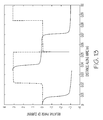
- FIG. 8 is a graph of induced current with respect to distance along a conductive element suitable for presentation on the display device in the computing system of FIG. 2 ;
- FIG. 9 is a graph depicting convergence results for a single wire transmission line corresponding to the excitation described in the context of FIG. 8 ;
- FIG. 10 is a graph of induced current with respect to distance along a conductive element in response to diffuse field excitation that is suitable for presentation on the display device in the computing system of FIG. 2 in conjunction with the induced field determination process of FIG. 3 ;
- FIG. 11 is a graph of induced current as a function of frequency corresponding to the excitation described in the context of FIG. 10 ;
- FIG. 12 is a graph of induced current with respect to distance along a conductive element illustrating the effect of varying the boundary conditions at one or more ends of the conductive element;
- FIG. 13 is a graph of the phase of the induced currents depicted in FIG. 12 with respect to distance along the conductive element illustrating the effect of varying the boundary conditions at one or more ends of the conductive element;
- FIG. 14 is a graph of induced voltage with respect to distance along the conductive element illustrating the effect of varying the boundary conditions at one or more ends of the conductive element;
- FIG. 15 is a graph of induced current with respect to distance along a conductive element in response to a diffuse field excitation that is suitable for presentation on the display device in the computing system of FIG. 2 in conjunction with the induced field determination process of FIG. 3 ;
- FIG. 16 is a graph of induced current with respect to a termination resistance in response to the diffuse field excitation described in the context of FIG. 15 ;
- FIG. 17 is a graph of induced current with respect to distance along a conductive element in response to a diffuse field excitation for a two wire transmission line with a short circuit at each end.
- FIG. 1 depicts a simplified representation of an exemplary operative environment having an electromagnetic radiation source 100 capable of inducing electromagnetic fields in a conductive element 102 within an enclosing body 104 .
- the electromagnetic radiation source 100 may be any source of electromagnetic radiation, such as for example, cellular base stations, wireless networks, cellular devices, wireless devices, Bluetooth devices, or other radio frequency (RF) transmitting devices. Accordingly, the subject matter described herein is not intended to be limited to any particular type of electromagnetic radiation source or any particular excitation frequency for the emitted electromagnetic waves.
- FIG. 1 depicts a simplified representation of an exemplary operative environment having an electromagnetic radiation source 100 capable of inducing electromagnetic fields in a conductive element 102 within an enclosing body 104 .
- the electromagnetic radiation source 100 may be any source of electromagnetic radiation, such as for example, cellular base stations, wireless networks, cellular devices, wireless devices, Bluetooth devices, or other radio frequency (RF) transmitting devices. Accordingly, the subject matter described herein is not intended to be limited to any particular type
- the electromagnetic radiation source 100 may be located outside the enclosing body 104 , in practice, the electromagnetic radiation source 100 may be located within the enclosing body 104 (e.g., a cellular phone or Bluetooth device inside the passenger cabin of an automotive vehicle).
- the electromagnetic radiation source 100 may be located within the enclosing body 104 (e.g., a cellular phone or Bluetooth device inside the passenger cabin of an automotive vehicle).
- the conductive element 102 represents any conductive element that is capable of having electromagnetic fields induced therein in response to electromagnetic radiation emitted by the electromagnetic radiation source 100 .
- the conductive element 102 may be realized as one or more wires, cables, transmission lines, conductive traces, electrical components, electronic circuits, or any suitable combination thereof. Accordingly, the subject matter described herein is not intended to be limited to any particular type or number of conductive elements. However, for purposes of explanation, the conductive element 102 may be described herein as being comprised of one or more wires (alternatively referred to as transmission lines) in a vehicle wiring system in an automotive vehicle application.
- the enclosing body 104 generally represents any enclosure or housing capable of containing or otherwise substantially enclosing the conductive element 102 to provide a substantially finite dielectric medium 110 surrounding the conductive element 102 . It should be understood that the subject matter described herein is not intended to be limited to any particular type of enclosing body and the conductive element 102 and/or dielectric medium 110 need not be perfectly enclosed (e.g., the enclosing body 104 need not be airtight or otherwise provide a continuous enclosure). For purposes of explanation, the enclosing body 104 may be described herein as an automotive vehicle.
- the electromagnetic wavefield (or waves) 106 emitted by the electromagnetic radiation source 100 induces or otherwise produces a corresponding electromagnetic wavefield 108 within the dielectric medium 110 confined by the vehicle body 104 .
- the electromagnetic wavefield 108 inside the vehicle body 104 can be approximated as an ideal diffuse wavefield, where there is an equal probability of electromagnetic waves propagating in all possible directions within the enclosing body 104 , which can be exploited to provide a computationally efficient technique for predicting the response of the conductive element 102 (e.g., the induced currents and/or voltages) to the reverberating electromagnetic wavefield 108 within the vehicle body 104 using the diffuse field reciprocity principle.
- the diffuse field reciprocity principle provides that the loading applied (e.g., the induced electric fields) by a random component (e.g., the electromagnetic wavefield 108 within the vehicle body 104 ) on a deterministic component (e.g., the conductive element 102 ) can be expressed in terms of the energy in the random component and the radiation properties of the deterministic component (i.e., the way in which the deterministic component would radiate into the random component, were the random component infinitely extended).
- a random component e.g., the electromagnetic wavefield 108 within the vehicle body 104
- a deterministic component e.g., the conductive element 102
- FIG. 2 depicts an exemplary embodiment of a computing system 200 capable of executing the processes, tasks, and functions described in greater detail below in the context of FIGS. 3-5 .
- the illustrated computing system 200 includes, without limitation, a user input device 202 , a processing system 204 , an output device 206 , and a computer-readable medium 208 . It should be understood that FIG. 2 is a simplified representation of a computing system for purposes of explanation and is not intended to limit the scope of the subject matter in any way.
- the user input device 202 generally represents the hardware and/or other components configured to provide a user interface with the computing system 200 .
- the user input device 202 may be realize as a key pad, a keyboard, one or more button(s), a touch panel, a touchscreen, an audio input device (e.g., a microphone), or the like.
- the output device 206 generally represents the hardware and/or other components configured to provide output to the user from the computing system 200 , as described in greater detail below.
- the output device 206 is realized as an electronic display device configured to graphically display information and/or content under control of the processing system 204 , as described in greater detail below.
- the processing system 204 generally represents the hardware, software, firmware, processing logic, and/or other components of the computing system 200 coupled to the user input device 202 and the display device 206 to receive input from the user, utilize the input provided by the user to execute various functions and/or processing tasks, and provide an output to the user, as described in greater detail below.
- the processing system 204 may be implemented or realized with a computer, a general purpose processor, a microprocessor, a controller, a microcontroller, a state machine, a content addressable memory, an application specific integrated circuit, a field programmable gate array, any suitable programmable logic device, discrete gate or transistor logic, discrete hardware components, or any combination thereof, designed to perform the functions described herein.
- the steps of a method or algorithm described in connection with the embodiments disclosed herein may be embodied directly in hardware, in firmware, in a software module executed by processing system 204 , or in any practical combination thereof.
- the computer-readable medium 208 may be realized as any non-transitory short or long term storage media capable of storing programming instructions or other data for execution by the processing system 204 , including any sort of random access memory (RAM), read only memory (ROM), flash memory, registers, hard disks, removable disks, magnetic or optical mass storage, and/or the like.
- RAM random access memory
- ROM read only memory
- flash memory registers, hard disks, removable disks, magnetic or optical mass storage, and/or the like.
- the computer-executable programming instructions when read and executed by the processing system 204 , cause the processing system 204 to execute one or more processes and perform the tasks, operations, and/or functions described in greater detail below in the context of FIGS. 3-5 .
- the processing system 204 executes the programming instructions stored or otherwise encoded on the computer-readable medium 208 , which causes the processing system 204 to display one or more graphical user interface elements (e.g., text boxes or the like) on the display device 206 that are adapted to receive user inputs indicative of the physical dimensions and/or physical layout of the conductive element 102 and the energy density and excitation frequency of the electromagnetic wavefield incident on the conductive element 102 (i.e., electromagnetic wavefield 108 ).
- graphical user interface elements e.g., text boxes or the like
- the processing system 204 may also display graphical user interface elements on the display device 206 that are adapted to receive user inputs indicative of the physical properties of the conductive element 102 and/or the dielectric medium 110 , such as, for example, the permeability of the conductive element 102 , the permittivity of the conductive element 102 , the conductance of the conductive element 102 , the permeability of the dielectric medium 110 , the volume of the dielectric medium 110 , and the like. Additionally, the processing system 204 may display graphical user interface elements on the display device 206 that are adapted to receive user inputs indicative of any boundary conditions (e.g., termination voltages and/or termination currents) to be applied to the conductive element 102 .
- any boundary conditions e.g., termination voltages and/or termination currents
- the user of the computing system 200 manipulates the user input device 202 to provide the physical dimensions and/or physical layout of the conductive element 102 and the energy density and excitation frequency of the incident electromagnetic wavefield 108 , along with any other desired inputs, to the processing system 204 .
- the user may manipulate the user input device 202 to select a graphical user interface element (e.g., a button or the like) that causes the processing system 204 to continue executing the programming instructions using the inputs received from the user.
- a graphical user interface element e.g., a button or the like
- the processing system 204 receives or otherwise obtains user inputs provided by the user and determines a surface electromagnetic impedance matrix for the conductive element 102 that corresponds to radiation from the surface of the conductive element 102 into an infinite dielectric medium and represents the relationship between the electric field and the magnetic field at the surface of the conductive element 102 , while at the same time imposing any boundary conditions provided by the user.
- the processing system 204 utilized the boundary conditions provided by the user to determine a voltage recovery matrix for the conductive element 102 . After determining the surface electromagnetic impedance matrix and voltage recovery matrix for the conductive element 102 , the processing system 204 applies the diffuse field reciprocity principle by multiplying the surface electromagnetic impedance matrix for the conductive element 102 by the energy density for the incident electromagnetic wavefield 108 to obtain a metric indicative of the mean square of the induced magnetic field at the surface of the conductive element 102 , which corresponds to the mean square induced current in the conductive element 102 , as described in greater detail below.
- mean square as used herein should be understood as encompassing the ensemble average of a time averaged second order product, where the ensemble corresponds to different realizations of the random incident electromagnetic field, as well as the “cross-spectrum” when the variable of interest is a vector rather than a scalar.
- the processing system 204 utilizes the mean square induced magnetic field and the voltage recovery matrix to determine the induced voltage in the conductive element 102 .
- the processing system 204 displays, on the display device, one or more graphical representations of the metrics indicative of the induced electric fields in the conductive element.
- the processing system 204 may display a plot or graph of the mean square induced current (or a variant thereof) with respect to a position or distance along the conductive element 102 , or a plot or graph of the induced voltage (or a variant thereof) with respect to a position or distance along the conductive element 102 , as described in greater detail below in the context of FIGS. 8 , 10 , 12 - 15 and 17 .
- FIG. 3 is a flow chart that illustrates an exemplary embodiment of an induced field determination process 300 suitable for calculating, determining, or otherwise estimating the induced electromagnetic fields, currents, and/or voltages induced by a diffuse electromagnetic wavefield (e.g., electromagnetic wavefield 108 ) in a conductive element (e.g., conductive element 102 ).
- the various tasks performed in connection with the illustrated process 300 may be performed by software, hardware, firmware, or any combination thereof.
- the following description of illustrated processes may refer to elements mentioned above in connection with FIG. 1 and FIG. 2 .
- process 300 may include any number of additional or alternative tasks, the tasks need not be performed in the illustrated order and/or the tasks may be performed concurrently, and/or the process 300 may be incorporated into a more comprehensive procedure or process having additional functionality not described in detail herein. Moreover, one or more of the tasks shown and described in the context of FIG. 3 could be omitted from an embodiment of the respective process as long as the intended overall functionality remains intact.
- the process 300 begins by obtaining parameters for the electromagnetic wavefield incident to the conductive element(s) being analyzed (task 302 ).
- a user provides (e.g., to processing system 204 via user input device 202 ) the electromagnetic energy density for the electromagnetic wavefield that is induced in the dielectric medium (e.g., electromagnetic wavefield 108 ) and incident on the conductive element(s) being analyzed (e.g., conductive element 102 ).
- the user provides the time averaged energy density (U) of the incident wavefield along with the excitation frequency ( ⁇ ) of the wavefield, which is utilized in conjunction with the permeability and volume of the dielectric medium (which may also be provided by the user, as described above) to determine the modal density (v) of electromagnetic modes in the dielectric medium surrounding the conductive element(s).
- the process 300 continues by obtaining the physical dimensions and/or layout of the conductive element(s) being analyzed (task 304 ).
- the process 300 receives of otherwise obtains from the user (e.g., via user input device 202 ) information that defines the physical dimensions (e.g., length, width, radius, and the like), shape, and/or structure of the conductive element(s) being analyzed.
- the user may also provide the distance (or spacing) between conductive elements. In this manner, the user defines the physical model of the conductive element(s) being analyzed.
- the process 300 continues by determining the surface electromagnetic impedance of the conductive element(s) based on the physical dimensions of the conductive element(s) and the excitation frequency for the incident wavefield (task 306 ). As described above and in greater detail below in the context of FIG. 4 , the process 300 determines an impedance matrix that is associated with electromagnetic radiation from the surface of the conductive element(s) into an infinite dielectric medium free of signal reflections.
- the surface electromagnetic impedance matrix is representative of the relationship between the electric field and the magnetic field at the surface of the conductive element(s).
- the electromagnetic impedance matrix for the conductive element(s) are determined in wavenumber space (or frequency domain) based on exact solutions to Maxwell's equations in cylindrical coordinates, as provide by equations (34)-(35) and (53)-(55) described below, using the input excitation frequency obtained from the user, as described in greater detail below with reference to with reference to equations (24)-(40).
- the electromagnetic impedance matrix is then transformed into the physical domain from wavenumber space based on the information pertaining to the physical dimensions of the conductive element(s), as described in greater detail below with reference to equations (73)-(78).
- the transformation from wavenumber space is accomplished using basis functions that are based on the sinc function.
- boundary conditions (which may be specified by the user) are imposed when determining the electromagnetic impedance matrix for conductive element(s) of finite length, as described in greater detail below with reference to equation (86).
- the process 300 continues by applying the diffuse field reciprocity principle using the surface electromagnetic impedance matrix and the excitation parameters to obtain a metric indicative of the magnetic field induced in the conductive element(s) by the incident electromagnetic wavefield (task 308 ).
- the process 300 determines one or more metrics indicative of the induced electric field(s) (e.g., an induced current metric, an induced voltage metric, or the like) in the conductive element (s) by the incident electromagnetic wavefield based on the induced magnetic field and provides an output indicative of the electric field(s) induced in the conductive element(s) by the incident electromagnetic wavefield (task 310 ).
- an incident wavefield energy metric is multiplied by the surface electromagnetic impedance to obtain a value indicative of the induced current(s) in the conductive element(s).
- the resistive part of the electromagnetic impedance matrix is multiplied by the time averaged energy density (U) of the incident wavefield and divided by the modal density (v) of electromagnetic modes in the dielectric medium surrounding the conductive element(s) to obtain a mean squared current induced in the conductive element(s) based on the mean (or ensemble average) of the square of the induced magnetic field on the surface of the conductive element(s), as described in greater detail below with reference to equations (1)-(18) and (92)-(93).
- the process 300 in addition to determining a metric indicative of the induced current in the conductive element(s) using the diffuse field reciprocity principle, the process 300 also determines a voltage recovery matrix for the conductive element(s) as described in greater detail below in the context of FIG. 5 and determines a metric indicative of the induced voltage in the conductive element(s) using the voltage recovery matrix and the induced magnetic field.
- the processing system 204 may display, present or otherwise provide one or more graphical representations of the current and/or voltage induced in the conductive element(s) on the display device 206 for review and analysis by the user.
- FIG. 4 is a flow chart that depicts an exemplary embodiment of a surface impedance matrix determination process 400 that may be performed (e.g., by processing system 204 as part of process 300 ) to determine an impedance matrix that is associated with electromagnetic radiation from the surface of a conductive element into an infinite dielectric medium.
- the various tasks performed in connection with the illustrated process 400 may be performed by software, hardware, firmware, or any combination thereof.
- the following description of illustrated processes may refer to elements mentioned above in connection with FIG. 1 and FIG. 2 .
- process 400 may include any number of additional or alternative tasks, the tasks need not be performed in the illustrated order and/or the tasks may be performed concurrently, and/or the process 400 may be incorporated into a more comprehensive procedure or process having additional functionality not described in detail herein. Moreover, one or more of the tasks shown and described in the context of FIG. 4 could be omitted from an embodiment of the respective process as long as the intended overall functionality remains intact.
- the process 400 begins by obtaining the excitation frequency for the incident electromagnetic wavefield and the physical dimensions of the conductive element (tasks 402 , 404 ). As described above in the context of FIG. 3 , in an exemplary embodiment, the excitation frequency for the incident electromagnetic wavefield and the physical dimensions of the conductive element are obtained from a user (e.g., via user input device 202 ). Using the excitation frequency and the physical dimensions of the conductive element, the process 400 continues by determining the surface electromagnetic impedance matrix for the conductive element in wavenumber space (or alternatively, the frequency domain) (task 406 ), as described in greater detail below with reference to equations (24)-(40).
- the process 400 continues by meshing the conductive element using the excitation frequency to determine a number of evenly spaced reference points along the longitudinal axis of the conductive element (task 408 ), as described in greater detail below with reference to equations (73)-(74), and then transforming the surface electromagnetic impedance matrix from wavenumber space to the physical domain (task 410 ) by performing a Fourier transform using the reference points, as described in greater detail below with reference to equations (75)-(78).
- the process 400 continues by applying boundary conditions to the transformed surface electromagnetic impedance matrix to obtain a modified surface electromagnetic impedance matrix in the physical domain (task 412 ), as described in greater detail below with reference to equation (86).
- the modified surface electromagnetic impedance matrix is utilized in the process 300 of FIG. 3 by applying the diffuse field reciprocity principle to the modified surface electromagnetic impedance matrix to determine metrics indicative of current induced in the conductive element, as described above and in greater detail below with reference to equations (92)-(93).
- FIG. 5 is a flow chart that depicts an exemplary embodiment of a voltage recovery matrix determination process 500 that may be performed (e.g., by processing system 204 as part of process 300 ) to determine a voltage recovery matrix for determining the induced voltage in a conductive element.
- the various tasks performed in connection with the illustrated process 500 may be performed by software, hardware, firmware, or any combination thereof.
- the following description of illustrated processes may refer to elements mentioned above in connection with FIG. 1 and FIG. 2 .
- the process 500 may include any number of additional or alternative tasks, the tasks need not be performed in the illustrated order and/or the tasks may be performed concurrently, and/or the process 500 may be incorporated into a more comprehensive procedure or process having additional functionality not described in detail herein.
- one or more of the tasks shown and described in the context of FIG. 5 could be omitted from an embodiment of the respective process as long as the intended overall functionality remains intact.
- the process 500 begins by obtaining the excitation frequency for the incident electromagnetic wavefield and the physical dimensions of the conductive element (tasks 502 , 504 ). As described above in the context of FIG. 3 , in an exemplary embodiment, the excitation frequency for the incident electromagnetic wavefield and the physical dimensions of the conductive element are obtained from a user (e.g., via user input device 202 ). Using the excitation frequency and the physical dimensions of the conductive element, the process 500 continues by determining the voltage recovery matrix for the conductive element in wavenumber space (or alternatively, the frequency domain) (task 506 ), as described in greater detail below with reference to equations (79)-(82).
- the process 500 continues by meshing the conductive element using the excitation frequency to determine a number of evenly spaced reference points along the longitudinal axis of the conductive element (task 508 ) in a similar manner as described herein in the context of the surface impedance matrix, and then transforms the voltage recovery matrix from wavenumber space to the physical domain (task 510 ), as described in greater detail below with reference to equations (83)-(85).
- the process 500 continues by applying boundary conditions to the transformed voltage recovery matrix to obtain a modified voltage recovery matrix in the physical domain (task 512 ), as described in greater detail below with reference to equation (87).
- the modified voltage recovery matrix is utilized in the process 300 of FIG. 3 to determine metrics indicative of voltage induced in the conductive element based on the induced magnetic field obtained by applying the diffuse field reciprocity principle, as described above and in greater detail below.
- FIG. 6 depicts a surface S representative of a conductive element (or a portion thereof), which consist of a number of cylindrical surfaces representing the combined surface of a multiple wire system.
- n(x) the unit normal vector pointing into the dielectric
- t 1 (x) and t 2 (x) two orthogonal unit tangent vectors
- the tangential components of the magnetic field can be expressed in terms of a finite number of generalized coordinates so that
- a set of generalized coordinates e jn can be introduced to describe the electric field, with the definition
- P (1 ⁇ 2) Re ( h* T e ).
- equation (8) It can be noted that a requirement for equation (8) to apply actually underlies the definition of the generalized coordinates given by equations (4) and (5). If the functions ⁇ n (x) are orthonormal, then equations (4) and (5) are mathematically alike, and there is no distinction between the definition of the generalized coordinates for the electric and magnetic fields.
- equation (4) can be inverted by using the method of weighted residuals to yield the generalized coordinates in terms of the magnetic field.
- the electromagnetic field in an infinite dielectric medium must satisfy Maxwell's equations. Taking the case in which there are no internal sources of electromagnetic radiation within the dielectric medium, and assuming that the Sommerfeld radiation conditions apply at infinity, these equations can be solved (analytically or numerically) to yield a relation between the tangential electric and magnetic field components on S.
- E[ ] represents the ensemble average, taken over realizations of the random diffuse field.
- Z DH is the impedance matrix associated with an infinite dielectric (i.e. with Sommerfeld radiation boundary conditions), while the diffuse waves are taken to be contained in a physical dielectric of finite extent; U is the time averaged energy of the diffuse field, and v is the modal density of electromagnetic modes in the dielectric (i.e. the average number of natural frequencies within a unit frequency band).
- the transmission line is composed of a number of wires of circular cross-section which each run parallel to the x 3 -axis.
- the present theory can be extended to include higher order waveguide modes, at the cost of additional algebraic complexity.
- the surface electric and magnetic fields are thus represented by field variables, e j (x 3 ) and h j (x 3 ) respectively, which depend only upon the coordinate x 3 , and these variables are taken to be ordered such that equation (8) applies, as described in greater detail below.
- the field variables are represented by generalized coordinates h jn and e jn , which are defined analogously to equations (4) and (5) in the form
- L is the domain of the transmission line.
- a dielectric impedance matrix in wavenumber space ⁇ circumflex over (Z) ⁇ D (k 3 ) say, can be defined such that
- a blocked electric field ê bj (k 3 ) can be defined as the Fourier transform of the blocked electric field in physical space, e bj (x 3 ).
- the impedance matrix Z D in generalized coordinates can be deduced by applying Parseval's theorem to equation (20) and then employing equation (23) to yield
- Z Djnrm ⁇ - ⁇ ⁇ ⁇ Z ⁇ Djr ⁇ ( k 3 ) ⁇ ⁇ ⁇ m ⁇ ( k 3 ) ⁇ ⁇ ⁇ n * ⁇ ( k 3 ) ⁇ d k 3 .
- the blocked electric field can be expressed in generalized coordinates as
- E ⁇ [ e bjn ⁇ e brm * ] ⁇ - ⁇ ⁇ ⁇ ⁇ - ⁇ ⁇ ⁇ E ⁇ [ e ⁇ bj ⁇ ( k 3 ) ⁇ e ⁇ br * ⁇ ( k 3 ′ ) ] ⁇ ⁇ ⁇ m ⁇ ( k 3 ′ ) ⁇ ⁇ ⁇ n * ⁇ ( k 3 ) ⁇ d k 3 ⁇ d k 3 ′ . ( 27 )
- H ⁇ ( x ) 1 2 ⁇ ⁇ ⁇ ⁇ ⁇ - k k ⁇ H ⁇ ⁇ ( x 1 , x 2 , k 3 ) ⁇ e i ⁇ ⁇ k 3 ⁇ x 3 ⁇ d k , ( 29 )
- E ⁇ [ ⁇ H ⁇ 2 ] 1 2 ⁇ ⁇ ⁇ ⁇ - k k ⁇ ⁇ - k k ⁇ E ⁇ [ H ⁇ ⁇ ( x 1 , x 2 , k 3 ) ⁇ H ⁇ * ⁇ ( x 1 , x 2 , k 3 ′ ) ] ⁇ e i ⁇ ( k 3 - k 3 ′ ) ⁇ x 3 ⁇ d k 3 ⁇ d k 3 ′ .
- Equations (31) and (32), together with equations (16) and (17), imply that equation (28) can be rewritten in the form ⁇ circumflex over (f) ⁇ bj ( ⁇ , ⁇ , k 3 ) ⁇ circumflex over (f) ⁇ * br ( ⁇ , ⁇ , k′ 3 ) ⁇ , ⁇ (2 ⁇ /k 2 ) ⁇ circumflex over (Z) ⁇ DHjr ( k 3 ). (33) If equation (33) is satisfied, then the diffuse field reciprocity equation (15) holds in generalized coordinates. The validity of equation (33) is explored below for a range of transmission lines and/or wiring configurations.
- the surface S consists of the cylindrical outer surface of the wire.
- TM transverse magnetic
- TE transverse electric
- the following analysis is restricted to the case of TM waves, since these waves are responsible for any axial current along the wire.
- equation (37) The negative sign is included in equation (37), together with the factor of 2 ⁇ a in equation (38), to ensure that the power radiated by the wire is given by equation (8).
- the variable given by equation (38) can be identified as the integral of the circumferential component of the magnetic field around the circumference of the wire, and from the Maxwell-Ampere law this is actually the current in the wire. It follows from equations (23), (37) and (38) that the impedance matrix of the dielectric (in this case a scalar) in wavenumber space is given by
- FIG. 7 depicts a simplified representation of a two wire transmission line system for purposes of explanation.
- the solution to Maxwell's equations in the dielectric medium can be represented as the sum of two sets of cylindrical waves, each set being centered on one of the wires.
- the electromagnetic field can be represented as a cylindrical wave of amplitude A 1 centered on the first wire, together with a cylindrical wave of amplitude A 2 centered on the second wire.
- equation (37) for the axial electric field variable on the surface of the first wire is modified to become
- Equations (59) and (62) can be used to explore the validity of equation (33) for the two wire system.
- Field variables ⁇ T (k 3 ) and ê T (k 3 ) can be defined for the transmission mode such that
- the impedance matrix Z D associated with an infinite dielectric medium surrounding a transmission line.
- the matrix Z C which appears in equation (13) is considered: this is the impedance matrix associated with the conducting material in the transmission line.
- the aim is not to demonstrate that the diffuse field reciprocity principle applies to this impedance, since clearly the conducting material will not carry a diffuse field, but rather to derive expressions for the electromagnetic impedance at the surface of the conducting material diffuse field reciprocity principle can be applied.
- the impedance (a scalar in this case) follows from a very similar argument to that used to derive the dielectric impedance, equation (39).
- the Hankel function H 0 (1) used to describe the outer solution to Maxwell's equations must be replaced by the Bessel function J 0 , and a sign change must be introduced to account for the direction of the inwards pointing normal; this procedure yields
- equation (72) is independent of k 3 , hence under this approximation the material is locally reacting, i.e. the Fourier transform of ⁇ circumflex over (Z) ⁇ C is proportional to the delta function ⁇ (x 3 ).
- the field variables for a single wire are represented by e 1 (x 3 ) and h 1 (x 3 ), while the field variables for the transmission mode response of a two wire system are represented by e T (x 3 ) and h T (x 3 ).
- the abbreviated notation e(x 3 ) and h(x 3 ) will be employed to represent either of these cases, and the corresponding generalized coordinates will be denoted by e n and h n .
- ⁇ ⁇ n ⁇ ( k 3 ) ⁇ ( ⁇ / 2 ) 1 / 2 ⁇ k s - 1 ⁇ e - i ⁇ ⁇ k s ⁇ x 3 , n ⁇ k 3 ⁇ ⁇ k s 0 ⁇ k 3 ⁇ > k s , ( 77 ) so that the dielectric impedance matrix in generalized coordinates follows from equation (25) as
- the exponent in equation (78) contains the term x 3,n ⁇ x 3,n which can also be written as (m ⁇ n) ⁇ x; this means that Z Dnm is a function of m ⁇ n.
- the impedance matrix can therefore be evaluated very efficiently by using the Fast Fourier Transform (FFT) algorithm.
- FFT Fast Fourier Transform
- the electromagnetic field generated by a single wire can be represented by a scalar potential ⁇ together with a vector potential A.
- C 1 and C 2 represent the circumferences of the wires in the x 1 -x 2 plane
- d is the distance between the wire centers.
- each end of the line is short-circuited by applying a symmetry boundary condition, which yields non-zero end currents and zero end voltages.
- An impedance is then added to each end of the line, thus allowing general boundary conditions to be modelled; for example, a zero added impedance maintains the short circuit condition, whereas an infinite added impedance recovers the zero current condition.
- Equation (86) and (87) imposes a short circuit at the left hand end of the line.
- H is the Heavyside step function
- R is an impedance (a real value of R would represent a resistance).
- Z R Rcc T . (91)
- a surface electric field e(x 3 ) has units of volts/m
- a generalized electric field variable e n has units of volts
- a surface magnetic field h(x 3 ) and a generalized magnetic field variable h n each have units of amps
- all impedance matrices Z have units of ohms
- the impedance R has units of ohms and is equivalent to a simple end impedance that would be employed in a transmission line analysis based on the telegrapher's equations.
- E ⁇ [ hh * T ] ( 2 ⁇ ⁇ ⁇ ⁇ c ⁇ ⁇ ⁇ ⁇ 2 ) ⁇ E ⁇ [ ⁇ E ⁇ 2 ] ⁇ ( Z DS + Z CS + Z R ) - 1 ⁇ Z DH ⁇ ( Z DS + Z CS + Z R ) - T * , ( 92 )
- 2 ] is the mean square value of the modulus of the electric field vector of the incident wavefield at any point in the enclosing body surrounding the transmission line.
- the default condition is zero current at each end of the wire, as illustrated in FIG. 8 .
- FIG. 9 illustrates convergence results for a single wire transmission line showing the maximum current in the wire as a function of the number of reference points per electromagnetic wavelength 2 ⁇ /k.
- the present method does not suffer from mesh density issues associated with the standard thin wire method of moments approach, in which the segment length must be at least eight to ten times the wire radius to avoid violating the assumptions inherent in the method, which places a limitation on the number of segments which can be employed, and hence the degree of convergence which can be attained.
- the use of 20 reference points per wavelength produces a maximum root mean square (rms) current which is 10% below that predicted by the use of 600 reference points per wavelength.
- the incident diffuse field is fully characterized by the frequency of oscillation (or equivalently k) and the ensemble mean squared value of the modulus of the electric field, which has the same value at every point in the field.
- the ensemble average of the modulus squared current at any point on the wire can be computed from equation (92), and the results which follow concern the square root of this quantity, referred to here as the root mean square (rms) current, which varies along the wire.
- the root mean square (rms) current which varies along the wire.
- the maximum rms current in the wire is plotted against the number of reference points used in the numerical model. It can be seen that the convergence rate for the case of diffuse field excitation is slightly slower than that for a concentrated voltage source, which is illustrated by the solid line in FIG. 9 .
- the response of the wire to electromagnetic excitation can be considered to consist of two components, a particular integral and a complementary function.
- the particular integral is the response of an infinite wire to diffuse field excitation
- the complementary function is the additional response needed to match the end boundary conditions.
- the complementary function tends to increase the rms current for the cases shown in FIG. 10 .
- the combined response will depend upon the relative phase between the two components of the response, and this issue is illustrated in FIG. 11 , which shows the spatial average of the rms current as a function of frequency; it can be seen that at some frequencies the response of an infinite wire exceeds that of the finite system.
- the graphical representation of the induced current depicted in FIG. 10 is one potential output that may be generated by the process 300 (e.g., task 310 ).
- the user may provide to the processing system 204 , via user input device 202 , the parameters defining the incident electromagnetic wavefield 108 and the length of the conductive element 102 , wherein the processing system 204 subsequently executes the processes or otherwise performs the equations described above to obtain the induced current as a function of the distance (or relative position) along the conductive element and generates a graphical representation of the induced current that is provided to or otherwise displayed on the display device 206 .
- FIG. 13 is a graphical representation of the phase of the relative current as a function of distance along the wire, and FIG.
- FIGS. 12-14 is a graphical representation of the voltage as a function of distance along the wire.
- the solid line represents results for zero current at the right hand end.
- each of the graphical representations depicted in FIGS. 12-14 is a potential output that may be generated by the process 300 (e.g., task 310 ).
- the results illustrated in FIGS. 12-14 were obtained using the approaches described above based on equation (65).
- a symmetry boundary condition was applied to allow the current to be non-zero, as described above.
- the applied voltage was then modelled as an axial electrical field of strength 1/(4l) applied to each wire in opposite directions over the region
- ⁇ l, with l 0.0175 m.
- the solid line represents the boundary conditions of zero current at each end of the wire
- the dashed line represents the boundary conditions of zero voltage (i.e., a short circuit) at each end of the wire
- the dotted line represents the boundary conditions of zero current at the right hand end of the wire and a short circuit at the left hand end.
- the results depicted in FIG. 15 are obtained by employing the transmission mode impedances, based on equations (65) and (69), in the response expression provided by equation (92).
- the dash-dot line in FIG. 15 illustrates the rms transmission mode current induced in an infinite transmission line, as given by equation (93). It can be seen that the maximum transmission mode current in the wire depends on the detailed boundary conditions, although the response of the infinite line, which can be computed very rapidly compared to the response of the finite line, yields a good first approximation of the general magnitude of the current; this is also the case for the previous example of a single wire, as evidenced by FIGS. 10-11 .
- FIG. 16 illustrates the effect of adding a resistor to the left hand end of the transmission line, obtained via equation (91), for the two cases of a short circuit at the right hand end, illustrated by the dashed line, and a zero current at the right hand end, illustrated by the solid line, wherein the dash-dot line represents the corresponding result for a transmission line of infinite length obtained via equation (93).
- This example is indicative of the way in which the impedance of a device attached to the end of the wire can affect the current flow into the device.
- diffuse field excitation of the two wire system can induce an antenna mode current.
- the complete current can be calculated by considering the full impedance matrix of the system, given by equation (59), rather than the reduced scalar impedance associated with the transmission mode, given by equation (65).
- the full impedance matrix in wavenumber space, obtained from equation (59) can be transformed to physical space by placing a grid of evenly spaced reference points along each wire, and assigning an independent generalized coordinate h n to each reference point.
- Equation (2) If there are N reference points on each wire then the model will have 2N degrees of freedom, and the associated 2N ⁇ 2N impedance matrix can be computed by employing equation (25) in conjunction with the wavenumber space impedance matrix from equation (59). The diffuse field reciprocity relation can then be used to compute the response of the system via equation (92).
- the solid line represents the total current
- the dashed line represents the transmission mode current
- the dotted line represents the antenna mode current.
- the result for the transmission mode current is in agreement with that shown in FIG. 15
- the antenna mode current is greater than the transmission mode current.
- the maximum of total current in the wire has an rms value that is around twice the maximum rms transmission mode current.
- the presence of the antenna mode can significantly affect the current in the interior of the wire, although only the transmission mode will affect the current drawn at the terminations.
- the present example demonstrates that the diffuse field reciprocity principle can be employed to yield all components of the current induced in the system.
- the diffuse field reciprocity principle states that the excitation applied to a system by a diffuse electromagnetic field can be expressed in terms of the surface electromagnetic impedance matrix of the system, as represented by equation (15).
- the surface electromagnetic impedance matrix of a wire system can be formulated in terms of exact solutions to Maxwell's equations in cylindrical coordinates; results in the frequency domain (or wavenumber space) have been presented above for one- and two wire systems respectively, and a numerical approach for expressing these results in the spatial domain has also been provided.
- the subject matter described herein may be extended to models of various different wiring systems and cable networks.
- the diffuse field reciprocity principle allows the rms currents induced by a diffuse electromagnetic field to be computed in a straight forward and efficient way.
- predicting the response of the wire to diffuse field excitation is a relatively trivial computational step as compared to previous approaches, such as those requiring a full computation of the electromagnetic field in the surrounding enclosure.
- the response computed by using the diffuse field reciprocity principle will be substantially identical to the result yielded by a “direct” calculation in which the diffuse electromagnetic field is represented as a summation of random plane waves (e.g., by calculating the excitation arising from individual plane waves and summing the response arising from each plane wave component), which requires a significant amount of computation time, since a sufficient number of waves with varying heading, azimuth, and polarization angle must be considered to produce an adequate representation of the diffuse field.
- the present approach immediately provides a statistically averaged result, whereas other approaches would require multiple randomized computations to generate an ensemble of results which can then be averaged to yield mean square values.
- an embodiment of a system or a component may employ various integrated circuit components, e.g., memory elements, digital signal processing elements, logic elements, look-up tables, or the like, which may carry out a variety of functions under the control of one or more microprocessors or other control devices.
- integrated circuit components e.g., memory elements, digital signal processing elements, logic elements, look-up tables, or the like, which may carry out a variety of functions under the control of one or more microprocessors or other control devices.
Abstract
Description
E(x)=E 1(x)t 1(x)+E 2(x)t 2(x)+E n(x)n(x), (1)
H(x)=H 1(x)t 1(x)+H 2(x)t 2(x)+H n(x)n(x). (2)
The field components are taken to be harmonic in time with frequency ω, and the variables in equations (1) and (2) are taken to represent complex amplitudes so that, for example, the time history of the first tangential electric component E1 is given by Re{E1e−iωt}. With this notation, the time average of the total electromagnetic power radiated by the surface can be written as
where φn(x) (n=1, 2, . . . , ∞) is a complete set of basis functions defined over the surface S, and hjn(n=1, 2, . . . , N) is a finite set of generalized coordinates used to approximate the magnetic field component Hj(x). Similarly, a set of generalized coordinates ejn can be introduced to describe the electric field, with the definition
The tangential field components can then represented by the vectors
where e1, for example, contains the generalized coordinates e1n. The ordering of the components in equations (6) and (7) has been chosen so that, by virtue of equations (3)-(5), the following relation holds:
P=(½)Re(h* T e). (8)
It can be noted that a requirement for equation (8) to apply actually underlies the definition of the generalized coordinates given by equations (4) and (5). If the functions φn(x) are orthonormal, then equations (4) and (5) are mathematically alike, and there is no distinction between the definition of the generalized coordinates for the electric and magnetic fields. However, in many approximate methods (for example the finite element method) the functions φn(x) are not orthonormal, and in this case the magnetic field generalized coordinates are not given by the magnetic equivalent of equation (5); rather, equation (4) can be inverted by using the method of weighted residuals to yield the generalized coordinates in terms of the magnetic field.
Z D h=e. (9)
Now the impedance matrix can be expressed as the sum of a Hermitian component ZDH and an anti-Hermitian component ZDA so that
Z D=(Z D +Z* D T)/2+(Z D −Z* D T)/2=Z DH +Z DA. (10)
One physically significant feature of these two components is that the power radiated by the surface is determined completely by ZDH, since it follows from equations (8)-(10) that
P=(½)h* T Z DH h. (11)
In acoustical or mechanical terminology, ZDH is referred to as the resistive part of the impedance matrix, associated with waves which propagate to infinity, while ZDA is referred to as the reactive part, associated with near-field effects. Two extensions to equation (9) are now considered: (i) the addition of incident electromagnetic waves in the dielectric, and (ii) the inclusion of the impedance matrix, ZC say, associated with the material that lies within the surface S. This leads to the pair of equations
Z D(h−h inc)=e−e inc , Z C h=−e, (12, 13)
where e and h are the total field components on S, and einc and hinc are the field components arising from the incident electromagnetic waves (in the absence of any reflection or diffraction at S). The sign convention associated with equation (13) is chosen to ensure that the power given by the analogy of equation (11) is in the direction of the inwards pointing normal vector, i.e. into the material associated with the impedance matrix. Now equations (12) and (13) yield
(Z D +Z C)h=Z D h inc −e inc =−e b, (14)
where eb is referred to herein as the blocked electric field, i.e., the surface tangential electric field that would result were the inner material such that h=0. The terminology “blocked” is often used in acoustics; for example the blocked acoustic pressure in a sound field containing an object is defined as the pressure obtained when the acoustic velocity normal to the surface of the object is enforced to be zero. In the present context the electric and magnetic fields are loosely analogous to the acoustic pressure and the normal velocity.
where E[ ] represents the ensemble average, taken over realizations of the random diffuse field. In this result, ZDH is the impedance matrix associated with an infinite dielectric (i.e. with Sommerfeld radiation boundary conditions), while the diffuse waves are taken to be contained in a physical dielectric of finite extent; U is the time averaged energy of the diffuse field, and v is the modal density of electromagnetic modes in the dielectric (i.e. the average number of natural frequencies within a unit frequency band). These quantities are given by
U=(½)μVE[|H| 2 ], v=Vω 2/(λ2 c 3), (16, 17)
where μ and V are respectively the permeability and volume of the dielectric, c is the speed of light, and ω is the frequency (in radians) of the incident wavefield. It can be noted that a diffuse field is by definition statistically homogenous, and so E[|H|2] is independent of spatial position. Equation (15) in conjunction with equation (14) yields a very efficient solution for the cross-spectrum of the surface magnetic field induced by the incident diffuse wavefield:
where L is the domain of the transmission line. In the detailed analysis of transmission lines it is analytically convenient to consider the Fourier transform of the field variables, so that, for example, the Fourier transform ĥj(k3) is considered rather than hj(x3), where
and k3 is the wavenumber in the x3-direction. With this notation, a dielectric impedance matrix in wavenumber space, {circumflex over (Z)}D(k3) say, can be defined such that
Likewise, a blocked electric field êbj(k3) can be defined as the Fourier transform of the blocked electric field in physical space, ebj(x3).
where the final equality in this result arises from the definition of ZD. Hence
The blocked electric field can be expressed in generalized coordinates as
and it follows that
E[ê bj(k 3)ê* br(k′ 3)]=(4U/πv)δ(k 3 −k′ 3){circumflex over (Z)} DHjr(k 3), (28)
where {circumflex over (Z)}DH(k3) is the Hermitian part of {circumflex over (Z)}D(k3). This equation can be simplified slightly by considering the nature of the incident diffuse field which gives rise to the blocked electric field. The magnetic field associated with the diffuse field can be written in terms of its Fourier transform in the form
where k=ω/c is the wavenumber of each wave component of the diffuse field, and it has been noted that the projected wavenumber k3 cannot exceed k. It follows that
The left hand side of equation (30) is independent of x, since the diffuse field is statistically homogeneous, and furthermore for a three-dimensional diffuse field the energy in the field is evenly distributed among the wavenumbers k3. Applying these considerations to equation (30) leads to the conclusion that
E[Ĥ(x 1 ,x 2 ,k 3)·{circumflex over (H)}*(x 1 ,x 2 ,k′ 3)]=(π/k)E[|H| 2]δ(k 3 −k′ 3). (31)
E[ê bj(k 3)ê* br(k′ 3)]=
where the first term on the right hand side represents an average over the azimuth and polarization angles. Equations (31) and (32), together with equations (16) and (17), imply that equation (28) can be rewritten in the form
If equation (33) is satisfied, then the diffuse field reciprocity equation (15) holds in generalized coordinates. The validity of equation (33) is explored below for a range of transmission lines and/or wiring configurations.
E z =AH 0 (1)(λa)e ik
H θ =A(ik 2/μωλ)H 0 (1)′(λa)e ik
where a is the radius of the wire, A is the cylindrical wave amplitude, and
λ=(k 2 −k 3 2)1/2. (36)
The field variables in wavenumber space, êj(k3) and ĥj(k3) (discussed above), can now be defined on the basis of equations (34) and (35) as
ê 1(k 3)=−AH 0 (1)(λa), (37)
ĥ 1(k 3)=2πaA(ik 2/μωλ)H 0 (1)′(λa). (38)
The Hermitian part of the impedance is then
where the Bessel function Wronskian properties have been used to simplify the result.
H=H amp[cos ψn 1+sin ψn 2 ]e ik.x, (41)
E=H ampη[sin ψn 1−cos ψn 2 ]e ik.x, (42)
where η=√{square root over (μ/∈)} and
n 1=(−sin φ cos φ0), (43)
n 2=(−cos β cos φ−cos β sin φ sin β), (44)
k=(k cos φ sin βk sin φ sin βk 3). (45)
Here β is the angle of incidence to the x3-axis, φ is the azimuth angle of incidence, measured in the x1-x2 plane, and ψ is the polarization of the wave, measured in a plane perpendicular to the propagation direction. From these definitions, equation (36) can be rewritten as λ=k sin β. Now on the surface S, the Cartesian position vector x and two unit tangent vectors tz and tθ can be written in terms of the cylindrical polar angle θ in the form
x=(a cos θa sin θx 3), t z=(0 0 1), (46, 47)
t θ=(−sin θ cos θ0). (48)
With this notation, the n=0 axial surface component of the incident electric field is given by
and similarly, the n=0 circumferential surface component of the incident magnetic field is given by
By definition, {circumflex over (f)}b,1 is given by the value of êb,1 under the condition Hamp=1. It can therefore be shown that (for k3≦k)
where the Bessel function Wronskian properties have been employed. For k3>k the corresponding result is zero, in line with equation (40). It follows from equation (52) that equation (33) is satisfied, thus proving the validity of the diffuse field reciprocity principle for a single wire.
where the second term represents the contribution from the wave centered on the second wire, and the vector d joins the centers of the two wires as shown in
ê 1(k 3)=−A 1 H 0 (1)(λa)−A 2 H 0 (1)(λd)J 0(λa). (54)
where the angles θ and χ are shown in
where the matrices P1 and P2 are defined accordingly. The impedance matrix of the dielectric medium in wavenumber space then follows as
{circumflex over (Z)} D(k 3)ĥ=ê, {circumflex over (Z)} D(k 3)=P 1 P 2 −1. (58, 59)
The electric and magnetic fields arising from an incident plane wave can be derived by extending equations (49) and (50) to yield
and the blocked electric field is then given by
ê b =ê inc −{circumflex over (Z)} D ĥ inc. (62)
and it can then be shown from equations (56)-(59) that the associated impedance is given by
Now the blocked electric field associated with the transmission mode can be written in the form
and by definition the variable {circumflex over (f)}bT is given by this result under the condition Hamp=1. It thus follows that (for k3≦k)
and the diffuse field reciprocity principle is valid for the transmission mode in a two wire system.
and kc, μc, ∈c, and σc are, respectively, the wavenumber, permeability, permittivity and conductance of the wire material. For many conducting materials σc>>∈cω and equation (69) can be approximated as
As described above, the field variables for a single wire are represented by e1(x3) and h1(x3), while the field variables for the transmission mode response of a two wire system are represented by eT(x3) and hT(x3). For ease of explanation, the abbreviated notation e(x3) and h(x3) will be employed to represent either of these cases, and the corresponding generalized coordinates will be denoted by en and hn. It follows from equations (19), (20), and (73) that the generalized coordinates can be related to the values of the field variables at the reference points as follows
h n =h(x 3,n), e n=(π/k s)e(x 3,n). (75, 76)
Now, the Fourier transform of the shape functions is given by
so that the dielectric impedance matrix in generalized coordinates follows from equation (25) as
The exponent in equation (78) contains the term x3,n−x3,n which can also be written as (m−n)Δx; this means that ZDnm is a function of m−n. The impedance matrix can therefore be evaluated very efficiently by using the Fast Fourier Transform (FFT) algorithm. With this approach the integral in equation (78) is evaluated for a range of exponents ±pΔx, where p is an integer, and the results are then used to populate the matrix ZD. This approach can similarly be used to calculate the impedance matrix ZC of the conducting material.
{circumflex over (Φ)}(k 3)=−A(ik 3/λ2)H 0 (1)(λr). (79)
By extension, the scalar potential associated with a two wire transmission line can be written as
{circumflex over (Φ)}=−(ik 3/λ2){A 1 H 0 (1)(λr 1)+A 2 H 0 (1)(λr 2)}, (80)
where A1 and A2 are the amplitudes of the waves associated with the wires, and r1 and r2 are distances from the centers of the wires. The scalar potential represents a voltage measure, and for the transmission mode (A1=−A2) the voltage across the wires is therefore given by
where C1 and C2 represent the circumferences of the wires in the x1-x2 plane, and d is the distance between the wire centers. It follows from equations (57), (63) and (81) that the transfer function between the voltage and the surface magnetic field is given by
The relationship between the voltage and the surface magnetic field in generalized coordinates then follows by analogy with equations (24) and (25), so that
The matrix F can be computed numerically by analogy with equations (77) and (78), and thus the voltage across the transmission line can be found from equation (83), once the surface magnetic field, hTn=hT(x3,n), is known. As described above with reference to equation (38), the surface magnetic field variable can be identified as the current in the wire. Although not detailed here, equations similar to equations (82)-(85) can also be derived for the case of a single wire.
Z DSnm=(½)δ1nδ1m Z Dnm+[1−(δ1n+δ1m)/2]×[Z Dnm +Z D(2−n−m)], (86)
and δnm is the Kronecker delta. In deriving equation (86) it has been noted that the mirror image of the point x3,m is at a distance (m+n−2)Δx to the left of the point x3,n; the additional electric field at the point x3,n arising from the current at the image point is accounted for by the appearance of the term ZD(2−n−m) in equation (86). Special consideration is needed when n=1 and/or m=1, since in these cases at least one of the two points lies on the axis of symmetry, and this introduces various factors of ½, which are accounted for by the presence of the Kronecker delta terms in equation (86). A similar modification must be applied to the impedance matrix ZC of the conducting material to yield a new matrix ZCS.
F Snm =F nm+(1−δ1m)F(2−n−m). (87)
e gen(x 3)=(R/l)[H(x 3 +l)−H(x 3 −l)]{∫−l l h(x 3)dx 3/2l)}. (88)
Here H is the Heavyside step function, and R is an impedance (a real value of R would represent a resistance). The average current over the small region can be written in terms of the generalized current vector in the form
∫−l l h(x 3)dx 3/(2l)=c T h, (89)
where the vector c has the entries
c n=(2−δ1n−δnN)(2lk s)−1 ×{Si[k s(x 3,n +l)]−Si[k s(x 3,n −l)]}, (90)
with Si representing the sine integral function. With this notation, it follows that equation (88) can be enforced by adding the following matrix to ZDS:
Z R =Rcc T. (91)
A similar approach can be applied at the right hand end of the line x3=L, leading to further modifications which are analogous to equations (86)-(91).
where E[|E|2] is the mean square value of the modulus of the electric field vector of the incident wavefield at any point in the enclosing body surrounding the transmission line. For reference, it can be shown on the basis of equations (31)-(33) that the response of an infinite transmission line to diffuse field excitation is given by
Application of equations (92) and (93) will now be described below in the context of a number of different exemplary cases.
Claims (16)
Priority Applications (4)
| Application Number | Priority Date | Filing Date | Title |
|---|---|---|---|
| US13/227,330 US9117040B2 (en) | 2011-04-12 | 2011-09-07 | Induced field determination using diffuse field reciprocity |
| US14/826,000 US10338117B2 (en) | 2011-04-12 | 2015-08-13 | Induced field determination using diffuse field reciprocity |
| US14/971,652 US10379147B2 (en) | 2011-04-12 | 2015-12-16 | Apparatus and method for determining statistical mean and maximum expected variance of electromagnetic energy transmission between coupled cavities |
| US14/971,598 US10156599B2 (en) | 2011-04-12 | 2015-12-16 | Apparatus and method for determining statistics of electric current in an electrical system exposed to diffuse electromagnetic fields |
Applications Claiming Priority (2)
| Application Number | Priority Date | Filing Date | Title |
|---|---|---|---|
| US201161474367P | 2011-04-12 | 2011-04-12 | |
| US13/227,330 US9117040B2 (en) | 2011-04-12 | 2011-09-07 | Induced field determination using diffuse field reciprocity |
Related Child Applications (3)
| Application Number | Title | Priority Date | Filing Date |
|---|---|---|---|
| PCT/US2014/043492 Continuation-In-Part WO2014205397A1 (en) | 2011-04-12 | 2014-06-20 | Apparatus and method for determining statistical mean and maximum expected variance of electromagnetic energy transmission between coupled cavities |
| PCT/US2014/043482 Continuation-In-Part WO2014205391A1 (en) | 2011-04-12 | 2014-06-20 | Apparatus and method for determining statistics of electric current in an electrical system exposed to diffuse electromagnetic fields |
| US14/826,000 Continuation US10338117B2 (en) | 2011-04-12 | 2015-08-13 | Induced field determination using diffuse field reciprocity |
Publications (2)
| Publication Number | Publication Date |
|---|---|
| US20120265464A1 US20120265464A1 (en) | 2012-10-18 |
| US9117040B2 true US9117040B2 (en) | 2015-08-25 |
Family
ID=47007060
Family Applications (4)
| Application Number | Title | Priority Date | Filing Date |
|---|---|---|---|
| US13/227,330 Active 2034-04-29 US9117040B2 (en) | 2011-04-12 | 2011-09-07 | Induced field determination using diffuse field reciprocity |
| US14/826,000 Active 2032-08-02 US10338117B2 (en) | 2011-04-12 | 2015-08-13 | Induced field determination using diffuse field reciprocity |
| US14/971,652 Active 2032-05-27 US10379147B2 (en) | 2011-04-12 | 2015-12-16 | Apparatus and method for determining statistical mean and maximum expected variance of electromagnetic energy transmission between coupled cavities |
| US14/971,598 Active 2031-12-20 US10156599B2 (en) | 2011-04-12 | 2015-12-16 | Apparatus and method for determining statistics of electric current in an electrical system exposed to diffuse electromagnetic fields |
Family Applications After (3)
| Application Number | Title | Priority Date | Filing Date |
|---|---|---|---|
| US14/826,000 Active 2032-08-02 US10338117B2 (en) | 2011-04-12 | 2015-08-13 | Induced field determination using diffuse field reciprocity |
| US14/971,652 Active 2032-05-27 US10379147B2 (en) | 2011-04-12 | 2015-12-16 | Apparatus and method for determining statistical mean and maximum expected variance of electromagnetic energy transmission between coupled cavities |
| US14/971,598 Active 2031-12-20 US10156599B2 (en) | 2011-04-12 | 2015-12-16 | Apparatus and method for determining statistics of electric current in an electrical system exposed to diffuse electromagnetic fields |
Country Status (1)
| Country | Link |
|---|---|
| US (4) | US9117040B2 (en) |
Families Citing this family (7)
| Publication number | Priority date | Publication date | Assignee | Title |
|---|---|---|---|---|
| WO2014205391A1 (en) * | 2013-06-21 | 2014-12-24 | Wave Six, Llc | Apparatus and method for determining statistics of electric current in an electrical system exposed to diffuse electromagnetic fields |
| US9117040B2 (en) | 2011-04-12 | 2015-08-25 | Robin Stewart Langley | Induced field determination using diffuse field reciprocity |
| US10565326B2 (en) * | 2013-07-30 | 2020-02-18 | Sonelite Inc. | Methods and systems for determining response of a reverberant system |
| CN107843774B (en) * | 2017-11-08 | 2021-01-05 | 中国电子科技集团公司电子科学研究院 | Electromagnetic situation calculation imaging method and electromagnetic situation imaging system |
| CN109239457B (en) * | 2018-08-27 | 2021-04-23 | 电子科技大学 | Microwave surface resistance continuous spectrum testing device |
| CN110954959B (en) * | 2018-09-27 | 2021-11-05 | 中国石油化工股份有限公司 | Method for analyzing spherical transmitted wave characteristics and computer-readable storage medium |
| WO2021127734A1 (en) * | 2019-12-24 | 2021-07-01 | Commonwealth Scientific And Industrial Research Organisation | An apparatus for the measurement of ore in mine haul vehicles |
Citations (4)
| Publication number | Priority date | Publication date | Assignee | Title |
|---|---|---|---|---|
| US5189366A (en) | 1988-12-20 | 1993-02-23 | Loma Group Limited | Method and apparatus using a varying electromagnetic field for determining the nature, or a property of a non-metallic material |
| US5751600A (en) | 1995-06-28 | 1998-05-12 | Hitachi, Ltd. | Method and apparatus for the analysis of electromagnetics |
| US20030019291A1 (en) | 1998-08-14 | 2003-01-30 | Pchelnikov Yuriy N. | Electromagnetic method of liquid level monitoring |
| US20060279273A1 (en) | 2001-04-09 | 2006-12-14 | Satoshi Kazama | Measuring method for electromagnetic field intensity and apparatus therefor, measuring method for electromagnetic field intensity distribution and apparatus therefor, measuring method for current and voltage distributions and apparatus therefor |
Family Cites Families (13)
| Publication number | Priority date | Publication date | Assignee | Title |
|---|---|---|---|---|
| US7243054B2 (en) * | 1999-07-14 | 2007-07-10 | Wireless Valley Communications, Inc. | Method and system for displaying network performance, cost, maintenance, and infrastructure wiring diagram |
| US20080097730A1 (en) * | 2000-09-29 | 2008-04-24 | Canning Francis X | Sparse and efficient block factorization for interaction data |
| DE102005032141B4 (en) | 2005-07-07 | 2007-07-26 | Airbus Deutschland Gmbh | Method and device for determining the irradiation field strength in an aircraft |
| US7554339B2 (en) | 2006-12-01 | 2009-06-30 | The Boeing Company | Electromagnetic testing of an enclosure or cavity using a discrete frequency stir method |
| US7880355B2 (en) | 2006-12-06 | 2011-02-01 | General Electric Company | Electromagnetic variable transmission |
| US8024692B2 (en) | 2007-05-04 | 2011-09-20 | Mentor Graphics Corporation | Modeling the skin effect using efficient conduction mode techniques |
| JP5642678B2 (en) * | 2008-08-22 | 2014-12-17 | デューク ユニバーシティーDuke University | Metamaterials for surfaces and waveguides |
| US20100125438A1 (en) | 2008-11-15 | 2010-05-20 | Mathieu Audet | Method of scanning, analyzing and identifying electro magnetic field sources |
| EP2374013A2 (en) | 2009-01-05 | 2011-10-12 | Yeda Research and Development Co. Ltd. | Radiation pollution mapping system |
| US8543346B2 (en) * | 2009-05-29 | 2013-09-24 | Oracle America, Inc. | Near-isotropic antenna for monitoring electromagnetic signals |
| EP2506040A1 (en) * | 2011-04-01 | 2012-10-03 | Université Catholique De Louvain | Method and device for characterization of physical properties of a target volume by electromagnetic inspection. |
| WO2014205391A1 (en) | 2013-06-21 | 2014-12-24 | Wave Six, Llc | Apparatus and method for determining statistics of electric current in an electrical system exposed to diffuse electromagnetic fields |
| US9117040B2 (en) | 2011-04-12 | 2015-08-25 | Robin Stewart Langley | Induced field determination using diffuse field reciprocity |
-
2011
- 2011-09-07 US US13/227,330 patent/US9117040B2/en active Active
-
2015
- 2015-08-13 US US14/826,000 patent/US10338117B2/en active Active
- 2015-12-16 US US14/971,652 patent/US10379147B2/en active Active
- 2015-12-16 US US14/971,598 patent/US10156599B2/en active Active
Patent Citations (4)
| Publication number | Priority date | Publication date | Assignee | Title |
|---|---|---|---|---|
| US5189366A (en) | 1988-12-20 | 1993-02-23 | Loma Group Limited | Method and apparatus using a varying electromagnetic field for determining the nature, or a property of a non-metallic material |
| US5751600A (en) | 1995-06-28 | 1998-05-12 | Hitachi, Ltd. | Method and apparatus for the analysis of electromagnetics |
| US20030019291A1 (en) | 1998-08-14 | 2003-01-30 | Pchelnikov Yuriy N. | Electromagnetic method of liquid level monitoring |
| US20060279273A1 (en) | 2001-04-09 | 2006-12-14 | Satoshi Kazama | Measuring method for electromagnetic field intensity and apparatus therefor, measuring method for electromagnetic field intensity distribution and apparatus therefor, measuring method for current and voltage distributions and apparatus therefor |
Non-Patent Citations (6)
| Title |
|---|
| Andersen, J. Bach et al., "Room Electromagnetics", Apr. 2007, IEEE Antennas and Propagation Magazine, vol. 49, No. 2, IEEE. * |
| International Search Report and Written Opinion for PCT/US2014/043482, 14 pages, Oct. 10, 2014. |
| Ishimaru, Akira et al., "Sommerfeld and Zenneck Wave Propagation for a Finely Conducting One-Dimensional Rough Surface", Sep. 2000, IEEE Transactions on Antennas and Propagation, vol. 48 No. 9, IEEE. * |
| Langley, R. S., "On the Diffuse Field Reciprocity Relationship and Vibrational Energy Variance in a Random Subsystem at High Frequencies", Feb. 2007, Journal of Acoustic Society of America, Acoustic Society of America. * |
| Langley, Robin S., "A Reciprocity Approach for Computing the Response of Wiring Systems to Diffuse Electromagnetic Fields", Nov. 17, 2010, IEEE Transactions on Electromagnetic Compatibility, vol. 52, No. 4, IEEE. * |
| Shorter, P.J. et al., "On the Reciprocity Relationship Between Direct Field Radiation and Diffuse Reverberant Loading", Jan. 2005, Journal of Acoustic Society of America, Acoustic Society of America. * |
Also Published As
| Publication number | Publication date |
|---|---|
| US20150369844A1 (en) | 2015-12-24 |
| US20160103165A1 (en) | 2016-04-14 |
| US20160103167A1 (en) | 2016-04-14 |
| US10379147B2 (en) | 2019-08-13 |
| US20120265464A1 (en) | 2012-10-18 |
| US10156599B2 (en) | 2018-12-18 |
| US10338117B2 (en) | 2019-07-02 |
Similar Documents
| Publication | Publication Date | Title |
|---|---|---|
| US10338117B2 (en) | Induced field determination using diffuse field reciprocity | |
| Huttunen et al. | Solving Maxwell’s equations using the ultra weak variational formulation | |
| O'Reilly et al. | Energy stable and high-order-accurate finite difference methods on staggered grids | |
| JP2006053908A (en) | Simulation technique | |
| US7987076B2 (en) | Electromagnetic field simulator and electromagnetic field simulation program storage medium | |
| US9286419B2 (en) | Computer simulation of electromagnetic fields | |
| US20130289955A1 (en) | Computer simulation of electromagnetic fields | |
| Balin et al. | Boundary element and finite element coupling for aeroacoustics simulations | |
| Andriychuk | Antenna synthesis through the characteristics of desired amplitude | |
| US8849627B2 (en) | Computer simulation of electromagnetic fields | |
| US9589083B2 (en) | Computer simulation of electromagnetic fields | |
| Chen et al. | A memory-efficient implementation of perfectly matched layer with smoothly varying coefficients in discontinuous Galerkin time-domain method | |
| Xu et al. | Approach to the analysis and synthesis of cylindrical metasurfaces with noncircular cross sections based on conformal transformations | |
| JP2004038774A (en) | Method and program for analyzing electromagnetic environment and recording medium recorded with the program | |
| Godinho et al. | A numerical MFS model for computational analysis of acoustic horns | |
| Autrique et al. | Studies of an infinite element method for acoustical radiation | |
| Álvarez González | A discontinuous Galerkin finite element method for the time-domain solution of Maxwell equations | |
| US10565326B2 (en) | Methods and systems for determining response of a reverberant system | |
| Monk et al. | Phase-accuracy comparisons and improved far-field estimates for 3-D edge elements on tetrahedral meshes | |
| EP3008619A2 (en) | Computer simulation of electromagnetic fields | |
| JP7149510B2 (en) | Computing system, computing device and program | |
| Diwan et al. | Iterative solution with shifted Laplace preconditioner for plane wave enriched isogeometric analysis and finite element discretization for high-frequency acoustics | |
| WO2014205391A1 (en) | Apparatus and method for determining statistics of electric current in an electrical system exposed to diffuse electromagnetic fields | |
| Bernard | On the expression of the field scattered by a multimode plane | |
| Luo et al. | A fixed-point iteration method for High frequency helmholtz equations |
Legal Events
| Date | Code | Title | Description |
|---|---|---|---|
| AS | Assignment |
Owner name: BREMNER, PAUL G, CALIFORNIA Free format text: ASSIGNMENT OF ASSIGNORS INTEREST;ASSIGNORS:LANGLEY, ROBIN S;STRUCTURAL ACOUSTICS LTD;REEL/FRAME:033056/0146 Effective date: 20130930 Owner name: SONELITE INC., CALIFORNIA Free format text: ASSIGNMENT OF ASSIGNORS INTEREST;ASSIGNORS:LANGLEY, ROBIN S;STRUCTURAL ACOUSTICS LTD;REEL/FRAME:033056/0146 Effective date: 20130930 |
|
| AS | Assignment |
Owner name: LANGLEY, ROBIN S, GREAT BRITAIN Free format text: CORRECTIVE ASSIGNMENT TO CORRECT THE ASSIGNEES PREVIOUSLY RECORDED AT REEL: 033056 FRAME: 0146. ASSIGNOR(S) HEREBY CONFIRMS THE ASSIGNMENT;ASSIGNORS:LANGLEY, ROBIN S;STRUCTURAL ACOUSTICS LTD;REEL/FRAME:033329/0952 Effective date: 20130930 Owner name: BREMNER, PAUL G, CALIFORNIA Free format text: CORRECTIVE ASSIGNMENT TO CORRECT THE ASSIGNEES PREVIOUSLY RECORDED AT REEL: 033056 FRAME: 0146. ASSIGNOR(S) HEREBY CONFIRMS THE ASSIGNMENT;ASSIGNORS:LANGLEY, ROBIN S;STRUCTURAL ACOUSTICS LTD;REEL/FRAME:033329/0952 Effective date: 20130930 |
|
| STCF | Information on status: patent grant |
Free format text: PATENTED CASE |
|
| AS | Assignment |
Owner name: WAVE SIX, LLC, NEW YORK Free format text: ASSIGNMENT OF ASSIGNORS INTEREST;ASSIGNOR:LANGLEY, ROBIN S.;REEL/FRAME:037076/0530 Effective date: 20140523 |
|
| AS | Assignment |
Owner name: DASSAULT SYSTEMES SIMULIA CORP., RHODE ISLAND Free format text: MERGER;ASSIGNORS:DASSAULT SYSTEMES SIMULIA CORP.;WAVE SIX LLC;REEL/FRAME:043857/0678 Effective date: 20170928 |
|
| MAFP | Maintenance fee payment |
Free format text: PAYMENT OF MAINTENANCE FEE, 4TH YR, SMALL ENTITY (ORIGINAL EVENT CODE: M2551); ENTITY STATUS OF PATENT OWNER: SMALL ENTITY Year of fee payment: 4 |
|
| FEPP | Fee payment procedure |
Free format text: ENTITY STATUS SET TO UNDISCOUNTED (ORIGINAL EVENT CODE: BIG.); ENTITY STATUS OF PATENT OWNER: LARGE ENTITY |
|
| MAFP | Maintenance fee payment |
Free format text: PAYMENT OF MAINTENANCE FEE, 8TH YEAR, LARGE ENTITY (ORIGINAL EVENT CODE: M1552); ENTITY STATUS OF PATENT OWNER: LARGE ENTITY Year of fee payment: 8 |
|
| AS | Assignment |
Owner name: DASSAULT SYSTEMES AMERICAS CORP., MASSACHUSETTS Free format text: MERGER;ASSIGNOR:DASSAULT SYSTEMES SIMULIA CORP.;REEL/FRAME:066383/0536 Effective date: 20240101 |