US9099126B2 - System and method of forming spacer structures using ultra narrow magnetic head fabrication - Google Patents
System and method of forming spacer structures using ultra narrow magnetic head fabrication Download PDFInfo
- Publication number
- US9099126B2 US9099126B2 US13/954,791 US201313954791A US9099126B2 US 9099126 B2 US9099126 B2 US 9099126B2 US 201313954791 A US201313954791 A US 201313954791A US 9099126 B2 US9099126 B2 US 9099126B2
- Authority
- US
- United States
- Prior art keywords
- sensor structure
- magnetic head
- sidewalls
- recited
- height direction
- Prior art date
- Legal status (The legal status is an assumption and is not a legal conclusion. Google has not performed a legal analysis and makes no representation as to the accuracy of the status listed.)
- Active
Links
- 238000000034 method Methods 0.000 title claims description 86
- 125000006850 spacer group Chemical group 0.000 title claims description 40
- 238000004519 manufacturing process Methods 0.000 title description 2
- 230000008569 process Effects 0.000 claims description 43
- 238000003801 milling Methods 0.000 claims description 39
- 229920000642 polymer Polymers 0.000 claims description 31
- 239000010408 film Substances 0.000 claims description 21
- 239000000758 substrate Substances 0.000 claims description 21
- 239000000463 material Substances 0.000 claims description 19
- 239000010409 thin film Substances 0.000 claims description 11
- 238000005137 deposition process Methods 0.000 claims description 8
- 238000000151 deposition Methods 0.000 claims description 7
- 238000013500 data storage Methods 0.000 claims description 4
- 230000007246 mechanism Effects 0.000 claims description 4
- 239000010410 layer Substances 0.000 description 58
- 238000013459 approach Methods 0.000 description 39
- 238000001020 plasma etching Methods 0.000 description 15
- 239000011248 coating agent Substances 0.000 description 8
- 238000000576 coating method Methods 0.000 description 8
- 230000004907 flux Effects 0.000 description 8
- 238000003860 storage Methods 0.000 description 6
- 239000000725 suspension Substances 0.000 description 6
- 238000009413 insulation Methods 0.000 description 5
- OKTJSMMVPCPJKN-UHFFFAOYSA-N Carbon Chemical compound [C] OKTJSMMVPCPJKN-UHFFFAOYSA-N 0.000 description 4
- VYPSYNLAJGMNEJ-UHFFFAOYSA-N Silicium dioxide Chemical compound O=[Si]=O VYPSYNLAJGMNEJ-UHFFFAOYSA-N 0.000 description 4
- 229910052799 carbon Inorganic materials 0.000 description 4
- 239000000696 magnetic material Substances 0.000 description 4
- 238000013461 design Methods 0.000 description 3
- 230000001965 increasing effect Effects 0.000 description 3
- 230000035699 permeability Effects 0.000 description 3
- 238000012546 transfer Methods 0.000 description 3
- 230000007704 transition Effects 0.000 description 3
- ZAMOUSCENKQFHK-UHFFFAOYSA-N Chlorine atom Chemical compound [Cl] ZAMOUSCENKQFHK-UHFFFAOYSA-N 0.000 description 2
- SECXISVLQFMRJM-UHFFFAOYSA-N N-Methylpyrrolidone Chemical compound CN1CCCC1=O SECXISVLQFMRJM-UHFFFAOYSA-N 0.000 description 2
- 229910052581 Si3N4 Inorganic materials 0.000 description 2
- 238000001636 atomic emission spectroscopy Methods 0.000 description 2
- 238000000231 atomic layer deposition Methods 0.000 description 2
- QVGXLLKOCUKJST-UHFFFAOYSA-N atomic oxygen Chemical compound [O] QVGXLLKOCUKJST-UHFFFAOYSA-N 0.000 description 2
- 230000015572 biosynthetic process Effects 0.000 description 2
- 239000000460 chlorine Substances 0.000 description 2
- 229910052801 chlorine Inorganic materials 0.000 description 2
- 230000000694 effects Effects 0.000 description 2
- NBVXSUQYWXRMNV-UHFFFAOYSA-N fluoromethane Chemical compound FC NBVXSUQYWXRMNV-UHFFFAOYSA-N 0.000 description 2
- 230000000873 masking effect Effects 0.000 description 2
- TWNQGVIAIRXVLR-UHFFFAOYSA-N oxo(oxoalumanyloxy)alumane Chemical compound O=[Al]O[Al]=O TWNQGVIAIRXVLR-UHFFFAOYSA-N 0.000 description 2
- 229910052760 oxygen Inorganic materials 0.000 description 2
- 239000001301 oxygen Substances 0.000 description 2
- 235000012771 pancakes Nutrition 0.000 description 2
- 229910021420 polycrystalline silicon Inorganic materials 0.000 description 2
- 229920005591 polysilicon Polymers 0.000 description 2
- 238000011160 research Methods 0.000 description 2
- 239000000377 silicon dioxide Substances 0.000 description 2
- 235000012239 silicon dioxide Nutrition 0.000 description 2
- HQVNEWCFYHHQES-UHFFFAOYSA-N silicon nitride Chemical compound N12[Si]34N5[Si]62N3[Si]51N64 HQVNEWCFYHHQES-UHFFFAOYSA-N 0.000 description 2
- 238000013519 translation Methods 0.000 description 2
- 229910017107 AlOx Inorganic materials 0.000 description 1
- 229910015844 BCl3 Inorganic materials 0.000 description 1
- KZBUYRJDOAKODT-UHFFFAOYSA-N Chlorine Chemical compound ClCl KZBUYRJDOAKODT-UHFFFAOYSA-N 0.000 description 1
- XPDWGBQVDMORPB-UHFFFAOYSA-N Fluoroform Chemical compound FC(F)F XPDWGBQVDMORPB-UHFFFAOYSA-N 0.000 description 1
- 229910001030 Iron–nickel alloy Inorganic materials 0.000 description 1
- 239000004642 Polyimide Substances 0.000 description 1
- KJTLSVCANCCWHF-UHFFFAOYSA-N Ruthenium Chemical compound [Ru] KJTLSVCANCCWHF-UHFFFAOYSA-N 0.000 description 1
- 229910004205 SiNX Inorganic materials 0.000 description 1
- XUIMIQQOPSSXEZ-UHFFFAOYSA-N Silicon Chemical compound [Si] XUIMIQQOPSSXEZ-UHFFFAOYSA-N 0.000 description 1
- 229910003070 TaOx Inorganic materials 0.000 description 1
- NRTOMJZYCJJWKI-UHFFFAOYSA-N Titanium nitride Chemical compound [Ti]#N NRTOMJZYCJJWKI-UHFFFAOYSA-N 0.000 description 1
- NIXOWILDQLNWCW-UHFFFAOYSA-N acrylic acid group Chemical group C(C=C)(=O)O NIXOWILDQLNWCW-UHFFFAOYSA-N 0.000 description 1
- XAGFODPZIPBFFR-UHFFFAOYSA-N aluminium Chemical compound [Al] XAGFODPZIPBFFR-UHFFFAOYSA-N 0.000 description 1
- 229910052782 aluminium Inorganic materials 0.000 description 1
- PNEYBMLMFCGWSK-UHFFFAOYSA-N aluminium oxide Inorganic materials [O-2].[O-2].[O-2].[Al+3].[Al+3] PNEYBMLMFCGWSK-UHFFFAOYSA-N 0.000 description 1
- 239000003575 carbonaceous material Substances 0.000 description 1
- 238000001311 chemical methods and process Methods 0.000 description 1
- 238000005229 chemical vapour deposition Methods 0.000 description 1
- 238000004891 communication Methods 0.000 description 1
- 238000004590 computer program Methods 0.000 description 1
- 230000008021 deposition Effects 0.000 description 1
- 230000001627 detrimental effect Effects 0.000 description 1
- 238000010586 diagram Methods 0.000 description 1
- 238000005530 etching Methods 0.000 description 1
- 230000006870 function Effects 0.000 description 1
- 239000011521 glass Substances 0.000 description 1
- 230000001939 inductive effect Effects 0.000 description 1
- 230000010365 information processing Effects 0.000 description 1
- 239000011229 interlayer Substances 0.000 description 1
- 238000010884 ion-beam technique Methods 0.000 description 1
- 230000005415 magnetization Effects 0.000 description 1
- BPUBBGLMJRNUCC-UHFFFAOYSA-N oxygen(2-);tantalum(5+) Chemical compound [O-2].[O-2].[O-2].[O-2].[O-2].[Ta+5].[Ta+5] BPUBBGLMJRNUCC-UHFFFAOYSA-N 0.000 description 1
- 238000007747 plating Methods 0.000 description 1
- 229920001721 polyimide Polymers 0.000 description 1
- 239000002861 polymer material Substances 0.000 description 1
- 238000012545 processing Methods 0.000 description 1
- 229910052707 ruthenium Inorganic materials 0.000 description 1
- 230000035040 seed growth Effects 0.000 description 1
- 229910052710 silicon Inorganic materials 0.000 description 1
- 239000010703 silicon Substances 0.000 description 1
- 239000002210 silicon-based material Substances 0.000 description 1
- 238000004544 sputter deposition Methods 0.000 description 1
- 238000000992 sputter etching Methods 0.000 description 1
- 229910052715 tantalum Inorganic materials 0.000 description 1
- GUVRBAGPIYLISA-UHFFFAOYSA-N tantalum atom Chemical compound [Ta] GUVRBAGPIYLISA-UHFFFAOYSA-N 0.000 description 1
- MZLGASXMSKOWSE-UHFFFAOYSA-N tantalum nitride Chemical compound [Ta]#N MZLGASXMSKOWSE-UHFFFAOYSA-N 0.000 description 1
- 229910001936 tantalum oxide Inorganic materials 0.000 description 1
- FAQYAMRNWDIXMY-UHFFFAOYSA-N trichloroborane Chemical compound ClB(Cl)Cl FAQYAMRNWDIXMY-UHFFFAOYSA-N 0.000 description 1
Images


Classifications
-
- G—PHYSICS
- G11—INFORMATION STORAGE
- G11B—INFORMATION STORAGE BASED ON RELATIVE MOVEMENT BETWEEN RECORD CARRIER AND TRANSDUCER
- G11B5/00—Recording by magnetisation or demagnetisation of a record carrier; Reproducing by magnetic means; Record carriers therefor
- G11B5/127—Structure or manufacture of heads, e.g. inductive
- G11B5/33—Structure or manufacture of flux-sensitive heads, i.e. for reproduction only; Combination of such heads with means for recording or erasing only
- G11B5/39—Structure or manufacture of flux-sensitive heads, i.e. for reproduction only; Combination of such heads with means for recording or erasing only using magneto-resistive devices or effects
- G11B5/3903—Structure or manufacture of flux-sensitive heads, i.e. for reproduction only; Combination of such heads with means for recording or erasing only using magneto-resistive devices or effects using magnetic thin film layers or their effects, the films being part of integrated structures
- G11B5/3906—Details related to the use of magnetic thin film layers or to their effects
- G11B5/3929—Disposition of magnetic thin films not used for directly coupling magnetic flux from the track to the MR film or for shielding
- G11B5/3932—Magnetic biasing films
-
- G—PHYSICS
- G11—INFORMATION STORAGE
- G11B—INFORMATION STORAGE BASED ON RELATIVE MOVEMENT BETWEEN RECORD CARRIER AND TRANSDUCER
- G11B5/00—Recording by magnetisation or demagnetisation of a record carrier; Reproducing by magnetic means; Record carriers therefor
- G11B5/127—Structure or manufacture of heads, e.g. inductive
- G11B5/31—Structure or manufacture of heads, e.g. inductive using thin films
- G11B5/3163—Fabrication methods or processes specially adapted for a particular head structure, e.g. using base layers for electroplating, using functional layers for masking, using energy or particle beams for shaping the structure or modifying the properties of the basic layers
Definitions
- the present invention relates to data storage systems, and more particularly, this invention relates to magnetic heads having improved sensor structures and methods of forming thereof.
- the heart of a computer is a magnetic hard disk drive (HDD) which typically includes a rotating magnetic disk, a slider that has read and write heads, a suspension arm above the rotating disk and an actuator arm that swings the suspension arm to place the read and/or write heads over selected circular tracks on the rotating disk.
- the suspension arm biases the slider into contact with the surface of the disk when the disk is not rotating but, when the disk rotates, air is swirled by the rotating disk adjacent an air bearing surface (ABS) of the slider causing the slider to ride on an air bearing a slight distance from the surface of the rotating disk.
- ABS air bearing surface
- the write and read heads are employed for writing magnetic impressions to and reading magnetic signal fields from the rotating disk.
- the read and write heads are connected to processing circuitry that operates according to a computer program to implement the writing and reading functions.
- the volume of information processing in the information age is increasing rapidly.
- HDDs be able to store more information in their limited area and volume.
- a technical approach to this desire is to increase the capacity by increasing the recording density of the HDD.
- the further miniaturization of the various components presents its own set of challenges and obstacles.
- the miniaturization of read sensors in conventional products is limited by the processes currently used to form such components.
- the large sensor structures found in conventional products have several detrimental effects to their performance; one of which includes overlapping of adjacent tracks while reading, thereby introducing noise and signal distortion.
- the tall profile of conventional products results in undesirably long transition times while reading data.
- various embodiments described and/or suggested herein include an improved sensor structure and methods of forming such sensor structures.
- the sensor structures described below may implement a reduced width, narrower cross-sectional profile and more vertical sidewalls, thereby resulting in drastic improvements over the performance limitations of conventional products described immediately above.
- a magnetic head includes a sensor structure extending from an air bearing surface end thereof in a stripe height direction, the sensor structure having sidewalls on opposite sides thereof, the sidewalls extending between a top and a bottom of the sensor structure, the sidewalls extending in the stripe height direction, wherein a spacing between the sidewalls in a track width direction along the top of the sensor structure is about constant therealong in the stripe height direction.
- a magnetic head includes a sensor structure extending from an air bearing surface end thereof in a stripe height direction, the sensor structure having sidewalls on opposite sides thereof, the sidewalls extending between a top and a bottom of the sensor structure, the sidewalls extending in the stripe height direction, wherein a line edge roughness of at least one of the sidewalls of the sensor structure is less than about 1.5 nm.
- a method includes forming a polymer mask with a line edge roughness of less than about 1.5 nm above a substrate, the substrate including a thin film stack of sensor materials and a milling mask layer, depositing a spacer film above the polymer mask and exposed portions of the substrate using a conformal deposition process, performing a first subtractive process to define a spacer from the spacer film, performing a second subtractive process to define a milling mask from the milling mask layer using the spacer, performing a third subtractive process to define a sensor structure from the thin film stack of sensor materials using the milling mask.
- a magnetic data storage system such as a disk drive system, which may include a magnetic head, a drive mechanism for passing a magnetic medium (e.g., hard disk) over the magnetic head, and a controller electrically coupled to the magnetic head.
- a magnetic medium e.g., hard disk
- FIG. 1 is a simplified drawing of a magnetic recording disk drive system.
- FIG. 2A is a schematic representation in section of a recording medium utilizing a longitudinal recording format.
- FIG. 2B is a schematic representation of a conventional magnetic recording head and recording medium combination for longitudinal recording as in FIG. 2A .
- FIG. 2C is a magnetic recording medium utilizing a perpendicular recording format.
- FIG. 2D is a schematic representation of a recording head and recording medium combination for perpendicular recording on one side.
- FIG. 2E is a schematic representation of a recording apparatus adapted for recording separately on both sides of the medium.
- FIG. 3A is a cross-sectional view of one particular embodiment of a perpendicular magnetic head with helical coils.
- FIG. 3B is a cross-sectional view of one particular embodiment of a piggyback magnetic head with helical coils.
- FIG. 4A is a cross-sectional view of one particular embodiment of a perpendicular magnetic head with looped coils.
- FIG. 4B is a cross-sectional view of one particular embodiment of a piggyback magnetic head with looped coils.
- FIG. 5A is a partial cross-sectional view of a magnetic head according to one embodiment.
- FIG. 5B is a partial top-down view of the magnetic head in FIG. 5A along line 5 B- 5 B.
- FIGS. 6A-6F are partial cross-sectional views corresponding to process steps of forming a magnetic head according to one embodiment.
- FIG. 6G is a partial top down view of FIG. 6F taken along line 6 G- 6 G of FIG. 6F .
- Various embodiments described herein include an improved sensor structure and methods of forming such sensor structures.
- the improved sensor structures allow for more efficient read operations of the corresponding magnetic heads, depending on the desired embodiment.
- the reduced width, narrower cross-sectional profile and more vertical sidewalls of the sensor structures described below allow for improved functionality of a magnetic head, as will be discussed in further detail below.
- a magnetic head in one general embodiment, includes a sensor structure extending from an air bearing surface end thereof in a stripe height direction, the sensor structure having sidewalls on opposite sides thereof, the sidewalls extending between a top and a bottom of the sensor structure, the sidewalls extending in the stripe height direction, wherein a spacing between the sidewalls in a track width direction along the top of the sensor structure is about constant therealong in the stripe height direction.
- a magnetic head in another general embodiment, includes a sensor structure extending from an air bearing surface end thereof in a stripe height direction, the sensor structure having sidewalls on opposite sides thereof, the sidewalls extending between a top and a bottom of the sensor structure, the sidewalls extending in the stripe height direction, wherein a line edge roughness of at least one of the sidewalls of the sensor structure is less than about 1.5 nm.
- a method in yet another general embodiment, includes forming a polymer mask with a line edge roughness of less than about 1.5 nm above a substrate, the substrate including a thin film stack of sensor materials and a milling mask layer, depositing a spacer film above the polymer mask and exposed portions of the substrate using a conformal deposition process, performing a first subtractive process to define a spacer from the spacer film, performing a second subtractive process to define a milling mask from the milling mask layer using the spacer, performing a third subtractive process to define a sensor structure from the thin film stack of sensor materials using the milling mask.
- FIG. 1 there is shown a disk drive 100 in accordance with one embodiment of the present invention.
- a disk drive mechanism which may include a disk drive motor 118 .
- the magnetic recording on each disk is typically in the form of an annular pattern of concentric data tracks (not shown) on the disk 112 .
- the disk drive motor 118 preferably passes the magnetic disk 112 over the magnetic read/write portions 121 , described immediately below.
- At least one slider 113 is positioned near the disk 112 , each slider 113 supporting one or more magnetic read/write portions 121 , e.g., of a magnetic head according to any of the approaches described and/or suggested herein.
- Slide 113 is moved radially in and out over disk surface 122 so that portions 121 may access different tracks of the disk where desired data are recorded and/or to be written.
- Each slider 113 is attached to an actuator arm 119 by means of a suspension 115 .
- the suspension 115 provides a slight spring force which biases slider 113 against the disk surface 122 .
- Each actuator arm 119 is attached to an actuator 127 .
- the actuator 127 as shown in FIG. 1 may be a voice coil motor (VCM).
- the VCM comprises a coil movable within a fixed magnetic field, the direction and speed of the coil movements being controlled by the motor current signals supplied by controller 129 .
- the rotation of disk 112 generates an air bearing between slider 113 and disk surface 122 which exerts an upward force or lift on the slider.
- the air bearing thus counter-balances the slight spring force of suspension 115 and supports slider 113 off and slightly above the disk surface by a small, substantially constant spacing during normal operation.
- the slider 113 may slide along the disk surface 122 .
- control unit 129 comprises logic control circuits, storage (e.g., memory), and a microprocessor.
- the control unit 129 is electrically coupled (e.g., via wire, cable, line, etc.) to the one or more magnetic read/write portions 121 , for controlling operation thereof.
- the control unit 129 generates control signals to control various system operations such as drive motor control signals on line 123 and head position and seek control signals on line 128 .
- the control signals on line 128 provide the desired current profiles to optimally move and position slider 113 to the desired data track on disk 112 .
- Read and write signals are communicated to and from read/write portions 121 by way of recording channel 125 .
- disk storage systems may contain a large number of disks and actuators, and each actuator may support a number of sliders.
- An interface may also be provided for communication between the disk drive and a host (integral or external) to send and receive the data and for controlling the operation of the disk drive and communicating the status of the disk drive to the host, all as will be understood by those of skill in the art.
- an inductive write portion includes a coil layer embedded in one or more insulation layers (insulation stack), the insulation stack being located between first and second pole piece layers.
- a gap is formed between the first and second pole piece layers by a gap layer at an air bearing surface (ABS) of the write portion.
- the pole piece layers may be connected at a back gap. Currents are conducted through the coil layer, which produce magnetic fields in the pole pieces. The magnetic fields fringe across the gap at the ABS for the purpose of writing bits of magnetic field information in tracks on moving media, such as in circular tracks on a rotating magnetic disk.
- the second pole piece layer has a pole tip portion which extends from the ABS to a flare point and a yoke portion which extends from the flare point to the back gap.
- the flare point is where the second pole piece begins to widen (flare) to form the yoke.
- the placement of the flare point directly affects the magnitude of the magnetic field produced to write information on the recording medium.
- FIG. 2A illustrates, schematically, a conventional recording medium such as used with magnetic disc recording systems, such as that shown in FIG. 1 .
- This medium is utilized for recording magnetic impulses in or parallel to the plane of the medium itself.
- the recording medium, a recording disc in this instance comprises basically a supporting substrate 200 of a suitable non-magnetic material such as glass, with an overlying coating 202 of a suitable and conventional magnetic layer.
- FIG. 2B shows the operative relationship between a conventional recording/playback head 204 , which may preferably be a thin film head, and a conventional recording medium, such as that of FIG. 2A .
- FIG. 2C illustrates, schematically, the orientation of magnetic impulses substantially perpendicular to the surface of a recording medium as used with magnetic disc recording systems, such as that shown in FIG. 1 .
- the medium typically includes an under layer 212 of a material having a high magnetic permeability.
- This under layer 212 is then provided with an overlying coating 214 of magnetic material preferably having a high coercivity relative to the under layer 212 .
- FIG. 2D illustrates the operative relationship between a perpendicular head 218 and a recording medium.
- the recording medium illustrated in FIG. 2D includes both the high permeability under layer 212 and the overlying coating 214 of magnetic material described with respect to FIG. 2C above. However, both of these layers 212 and 214 are shown applied to a suitable substrate 216 . Typically there is also an additional layer (not shown) called an “exchange-break” layer or “interlayer” between layers 212 and 214 .
- the magnetic lines of flux extending between the poles of the perpendicular head 218 loop into and out of the overlying coating 214 of the recording medium with the high permeability under layer 212 of the recording medium causing the lines of flux to pass through the overlying coating 214 in a direction generally perpendicular to the surface of the medium to record information in the overlying coating 214 of magnetic material preferably having a high coercivity relative to the under layer 212 in the form of magnetic impulses having their axes of magnetization substantially perpendicular to the surface of the medium.
- the flux is channeled by the soft underlying coating 212 back to the return layer (PI) of the head 218 .
- FIG. 2E illustrates a similar structure in which the substrate 216 carries the layers 212 and 214 on each of its two opposed sides, with suitable recording heads 218 positioned adjacent the outer surface of the magnetic coating 214 on each side of the medium, allowing for recording on each side of the medium.
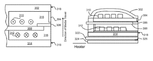
- FIG. 3A is a cross-sectional view of a perpendicular magnetic head.
- helical coils 310 and 312 are used to create magnetic flux in the stitch pole 308 , which then delivers that flux to the main pole 306 .
- Coils 310 indicate coils extending out from the page, while coils 312 indicate coils extending into the page.
- Stitch pole 308 may be recessed from the ABS 318 .
- Insulation 316 surrounds the coils and may provide support for some of the elements.
- the direction of the media travel moves the media past the lower return pole 314 first, then past the stitch pole 308 , main pole 306 , trailing shield 304 which may be connected to the wrap around shield (not shown), and finally past the upper return pole 302 .
- Each of these components may or may not have a portion in contact with the ABS 318 .
- the ABS 318 is indicated across the right side of the structure.
- Perpendicular writing is achieved by forcing flux through the stitch pole 308 into the main pole 306 and then to the surface of the disk positioned towards the ABS 318 .
- FIG. 3B illustrates a piggyback magnetic head having similar features to the head of FIG. 3A .
- Two shields 304 , 314 flank the stitch pole 308 and main pole 306 of the magnetic write portion.
- the read sensor shields 322 , 324 of the magnetic read portion are shown.
- the read sensor 326 is typically positioned between the sensor shields 322 , 324 .
- FIG. 4A is a schematic diagram of one embodiment which uses looped coils 410 , sometimes referred to as a pancake configuration, to provide flux to the stitch pole 408 .
- the stitch pole then provides this flux to the main pole 406 .
- the lower return pole is optional.
- Insulation 416 surrounds the coils 410 , and may provide support for the stitch pole 408 and main pole 406 .
- the stitch pole may be recessed from the ABS 418 .
- the direction of the media travel moves the media past the stitch pole 408 , main pole 406 , trailing shield 404 which may be connected to the wrap around shield (not shown), and finally past the upper return pole 402 (all of which may or may not have a portion in contact with the ABS 418 ).
- the ABS 418 is indicated across the right side of the structure.
- the trailing shield 404 may be in contact with the main pole 406 in some embodiments.
- FIG. 4B illustrates another type of piggyback magnetic head having similar features to the head of FIG. 4A including a looped coil 410 , which wraps around to form a pancake coil. Also, sensor shields 422 , 424 of the magnetic read portion are shown. The read sensor 426 is typically positioned between the sensor shields 422 , 424 .
- an optional heater is shown near the non-ABS side of the magnetic head.
- a heater may also be included in the magnetic heads shown in FIGS. 3A and 4A .
- the position of this heater may vary based on design parameters such as where the protrusion is desired, coefficients of thermal expansion of the surrounding layers, etc.
- any of the embodiments described and/or suggested above in relation to FIGS. 1-4B may include at least one such improved sensor structure according to any of the approaches described below.
- Some of the sensor structures described herein preferably include sidewalls having a low line edge roughness (LER), about constant spacing between the sidewalls thereof (e.g., symmetric sidewalls), and/or a smaller width than conventionally achievable.
- LER line edge roughness
- the improved sensor structures of the various embodiments herein are able to perform more detailed read operations, e.g., read narrower data tracks, make sharper transitions when reading data, etc.
- FIGS. 5A-5B depict a magnetic head 500 , in accordance with one embodiment.
- the present magnetic head 500 may be implemented in conjunction with features from any other embodiment listed herein, such as those described with reference to the other FIGS.
- the magnetic head 500 and others presented herein may be used in various applications and/or in permutations which may or may not be specifically described in the illustrative embodiments listed herein.
- the magnetic head 500 presented herein may be used in any desired environment.
- the magnetic head 500 includes a sensor structure 502 positioned above a shield 512 .
- an insulating layer 518 , hard bias layer 520 and second shield 522 are formed thereabove.
- the insulating layer 518 , hard bias layer 520 and second shield 522 may be formed using sputtering, chemical vapor deposition, plating, seed growth layers, etc., and/or any other process which would be apparent to one skilled in the art upon reading the present description.
- any of the layers illustrated in FIGS. 5A-5B including the sensor structure 502 , may be of any type known in the art.
- the sensor structure 502 preferably extends from an air bearing surface 504 end thereof in a stripe height direction Y.
- the sensor structure 502 also has sidewalls 506 on opposite sides thereof, where the sidewalls 506 may extend between a top and a bottom of the sensor structure 502 .
- the sidewalls 506 also extend in the stripe height direction Y.
- a preferred process of forming a sensor structure may result in a minimized LER of the sidewalls of the sensor structure. Moreover, the lowered LER of the sidewalls of the sensor structure allows for improved uniformity of the spacing therebetween in addition to an overall narrower sensor structure, as will soon become apparent.
- the spacing S 1 , S 2 between the sidewalls 506 in a track width direction X along the top and bottom of the sensor structure 502 respectively is preferably about constant therealong in the stripe height direction Y.
- “about constant” is intended to mean that the spacing between the sidewalls varies by no more than about 1 to about 2 nm therealong in the stripe height direction Y, depending on the designed spacing S 1 , S 2 , but may be higher or lower according to various approaches.
- an average spacing between the sidewalls of the sensor structure 502 along an X-Y plane at any thickness level of the sensor may be between about 3 nm and about 50 nm, but could be higher or lower depending on the desired embodiment.
- FIGS. 6A-6F illustrate preferred process steps of a method for forming a sensor structure having improved functionality, e.g., such as the sensor structure 502 shown in FIGS. 5A-5B , according to an exemplary embodiment.
- FIGS. 6A-6F depict process steps of a method for forming a magnetic head 600 having a sensor structure 502 , in accordance with one embodiment.
- the present method for forming a magnetic head 600 may be implemented in conjunction with features from any other embodiment listed herein, such as those described with reference to the other FIGS.
- the method for forming a magnetic head 600 and others presented herein may be used in various applications and/or in permutations which may or may not be specifically described in the illustrative embodiments listed herein.
- the method for forming a magnetic head 600 presented herein may be used in any desired environment.
- FIGS. 6A-6F (and the other FIGS.) should be deemed to include any and all possible permutations.
- the method for forming the magnetic head 600 includes forming a polymer mask 602 above a substrate 604 .
- the substrate 604 may include shield 606 , a thin film stack of sensor materials 608 and a milling mask layer 610 .
- the milling mask layer 610 may include carbon, a polymer-like carbon, silicon nitride, silicon dioxide, aluminum oxide, ruthenium, etc.
- the milling mask layer 610 may be laminated with silicon, tantalum oxide, tantalum, etc. depending on the desired embodiment.
- the laminate may act as a stop layer in some approaches, e.g., to stop a subtractive process before reaching the sensor materials 608 .
- the polymer mask 602 may have a LER of less than about 1.5 nm, more preferably less than about 1 nm, but could be higher or lower depending on the desired embodiment.
- the LER of the foundational layers, e.g., the polymer mask 602 may be translated to the other layers later formed, thereby influencing the structure of the sensor structure 502 .
- the polymer mask 602 may be formed by imprinting, e.g., using a patterned roller, stamper, etc.
- the polymer mask 602 may be formed by depositing a UV curable polymer (e.g., an acrylic) above the milling mask layer 610 . Thereafter, a template may be used to imprint (press) the polymer into a desired shape whereby a light source may be used to cure the pressed polymer material to form the polymer mask 602 .
- a UV curable polymer e.g., an acrylic
- a template may be used to imprint (press) the polymer into a desired shape whereby a light source may be used to cure the pressed polymer material to form the polymer mask 602 .
- the polymer mask 602 may be formed using any other method which may result in a desirable LER thereof.
- the polymer mask 602 may be formed of alternative materials known in the art, and that are amenable to sidewall definition by imprinting.
- the substrate 604 may include an additional layer (not shown) between the milling mask layer 610 and the polymer mask 602 , e.g., to protect the substrate 604 during the formation of the polymer mask 602 .
- Exposed portions of the additional layer may preferably be removed before any of the other process steps depicted in FIGS. 6B-6F are performed, e.g., using a reactive ion etching (RIE) procedure, wet etch, etc.
- RIE reactive ion etching
- the additional layer may be removed at a later step, or not at all, depending on the desired embodiment.
- the milling mask layer 610 may be present in the substrate, e.g., to reduce stress thereof.
- the milling mask layer 610 may have a thickness t 1 from about 5 nm to about 100 nm, but could be higher or lower.
- the polymer mask 602 may have a thickness t 2 from about 10 nm to about 100 nm, but may be higher or lower depending on the desired embodiment.
- the method also includes depositing a spacer film 612 above the polymer mask 602 and exposed portions of the substrate 604 .
- the spacer film 612 may include SiOC 2 , AlOx, SiNx, TaOx, NiFe, Ru, tantalum nitride, titanium nitride, polysilicon, etc.
- the spacer film 612 may be formed using a conformal deposition process, which may include using atomic layer deposition (ALD) and/or other such processes having the same or similar effects.
- ALD atomic layer deposition
- the conformal deposition process may ensure an about constant thickness t 3 of the spacer film 612 , as illustrated in FIG. 6B .
- the spacer film 612 may have a thickness t 3 from about 5 nm to about 100 nm, more preferably from about 3 nm to about 50 nm, but may be higher or lower depending on the desired embodiment.
- the spacer film 612 preferably has the same, or about the same, LER as the polymer mask 602 .
- the uniform nature of a conformal deposition process to form the spacer film 612 may result in the low LER value of the polymer mask 602 being translated through the spacer film 612 .
- the method also includes performing a first subtractive process to define a spacer 614 from the spacer film 612 .
- the first subtractive process may be twofold as suggested by FIGS. 6C-6D .
- the first subtractive process may be performed in a single step, e.g., using a single sub-process.
- the first step of the first subtractive process may include a directional RIE procedure, e.g., using fluorocarbon plasma, chlorine, etc.; a directional milling procedure, e.g., using an ion beam; etc.
- the remainder of the polymer mask 602 may be removed in a second step of the first subtractive process, thereby forming the spacer 614 from the spacer film 612 .
- the second step of the first subtractive process may include an oxygen based plasma ash and/or strip (e.g., non-biased), N-Methyl Pyrrolidone (NMP), etc., and/or any of those listed above with reference to the first step of the first subtractive process.
- the spacer 614 preferably retains the low LER of the previous spacer film 612 , despite the first subtractive process.
- the spacer 614 may have an LER value for at least one of its vertical sidewalls, more preferably each of its vertical sidewalls, of about 1.5 nm, more preferably about 1 nm.
- the thickness t 4 of the spacer 614 may be from about 3 nm to about 50 nm, but could be higher or lower depending on the desired embodiment.
- the about constant thickness and low LER of the spacer 614 are desirable as they result in translation of the low LER to the milling mask 616 and a reduced amount of shadowing observed when forming sensor structure 502 as will be discussed in further detail below.
- the process steps illustrated in FIGS. 6A-6F may allow for a desirably smaller spacing between the sidewalls 506 of the sensor structure 502 , in addition to about constant spacing S 1 , S 2 thereof, as mentioned above.
- the method for forming the magnetic head 600 also includes performing a second subtractive process to define a milling mask 616 from the milling mask layer 610 .
- the thickness t 1 of the milling mask 616 may be from about 3 nm to about 50 nm, but could be higher or lower depending on the desired embodiment.
- the spacer 614 may be used to perform the second subtractive process, e.g., define the milling mask 616 .
- the second subtractive process may include a RIE process.
- the RIE process may use an oxygen based RIE (e.g., O2, CO2, CO, etc., and/or combinations thereof) to transfer a mask pattern into the milling mask layer 610 if the mask layer 610 includes a carbon based material such as a polymer-like carbon, diamond-like carbon (DLC), polyimide, etc.
- the RIE process may use a fluorocarbon based RIE (e.g., CF4, CHF3, etc., and/or combination thereof) to transfer a mask pattern into the milling mask layer 610 if the mask layer 610 includes a silicon based material such as silicon nitride, silicon dioxide, polysilicon, etc.
- the RIE process may use a chlorine based RIE (e.g., Cl 2 , BCl 3 , etc. and/or combinations thereof) to transfer a mask pattern into the milling mask layer 610 if the mask layer 610 includes an aluminum based material such as aluminum oxide, alumina, etc.
- a mask pattern may be transferred into the milling mask layer 610 using other processes which would be apparent to one skilled in the art upon reading the present description.
- RIE tools equipped with both source and bias power suppliers such as TCP9400DFM from Lam Research Inc. (Lam Research Corporation, 4650 Cushing Parkway, Fremont, Calif. 94538), or DPS from Applied Materials Inc. (Applied Materials, Inc., 2821 Scott Boulevard, Santa Clara, Calif. 95050, or Plasma-Therm's VERSALOCK etcher (Plasma-Therm, 10050 16th St N, St City, Fla. 33716), may be used with any of the RIE processes described above.
- the separate source and bias power control in these RIE tools allows a wider range of RIE processes to be performed, ranging from highly chemical processes to highly physical processes.
- the Optical Emission Spectrometry (OES) endpoint system of these RIE tools allows to precisely control the over etch amount via the determination of etch endpoint.
- OFES Optical Emission Spectrometry
- the low LER value of the spacer 614 is translated onto the milling mask 616 during formation thereof.
- the milling mask 616 may have an LER value for at least one of its sidewalls, more preferably each of its sidewalls, of about 1.5 nm or lower, more preferably about 1 nm or lower.
- the milling mask 616 may have an even lower LER value than that of the polymer mask 602 and/or spacer 614 as a result of the preferred process steps illustrated in FIGS. 6A-6F .
- FIG. 6F illustrates the result of performing a third subtractive process to define the sensor structure 502 from the thin film stack of sensor materials 608 using the milling mask 616 .
- the third subtractive process may include ion milling to form the sensor structure 502 .
- the milling angle is between about 0 and about 20 degrees from orthogonal to the deposition plane of the sensor materials 608 .
- the third subtractive process may include any of the process steps described above in the first and/or second subtractive process, and/or a process which would be apparent to one skilled in the art upon reading the present description.
- an average spacing value S 2 between the sidewalls of the sensor structure 502 in the track width direction X along the bottom thereof may be between about 3 nm and about 50 nm, but could be higher or lower depending on the desired embodiment.
- the thickness t 5 of the sensor structure 502 may be from about 10 nm to about 50 nm, more preferably from about 5 nm to about 40 nm, but may be higher or lower depending on the desired embodiment.
- the reduced thickness of the sensor structure allows for sharper transitions when reading data.
- performance of the sensor structure 502 is improved.
- FIG. 6G which is a partial top down view of the structure shown in FIG. 6F , demonstrates the uniformity of the spacing between the sidewalls 506 of the sensor structure 502 .
- the curvature of the sidewalls of the sensor structure have been exaggerated for explanatory purposes.
- the LER of the original polymer mask 602 has a dramatic effect on the LER of the sensor structure via translation thereof through the various masking layers.
- the conformality of the spacer film and resulting spacer, and masking layer(s) formed therewith preferably results in the spacing between the sidewalls of the sensor structure 502 being about constant at any point along the height of the sensor structure when measured in the same plane. For example, S 1 , S 2 and/or any width therebetween may be about constant when measured at any point along the height of the sensor structure 502 .
- the LER of at least one of the sidewalls of the sensor structure 502 may be less than about 1.5 nm, more preferably less than about 1 nm, where “about” signifies ⁇ 20% of the referenced value for any value used herein, unless otherwise defined.
- the process steps illustrated in FIGS. 6A-6F allow for the sidewalls of the resulting sensor structure to have increased verticality, thereby improving functionality.
- the average angle ⁇ of the sensor sidewall from horizontal is between about 80 and 90 degrees.
- the milling mask 616 may be removed using any conventional process, and additional layers may be formed over the sensor structure 502 and shield 606 .
- additional layers may be formed over the sensor structure 502 and shield 606 .
- different process steps and/or configurations may be incorporated with the magnetic head 600 and/or fabrication thereof.
- the magnetic head 600 of FIG. 6F may include an insulating layer 518 , hard bias layer 520 and/or second shield 522 , e.g., using any process steps described above, and/or any of those which would be apparent to one skilled in the art upon reading the present description.
- an additional process step(s) may be performed in which excess portions of the magnetic head formed may be cut away, e.g., using masked etching, etc. to define the height thereof and/or the ABS.
- any of the process steps, materials, etc. may be of a type known in the art.
- any of the structures and/or steps may be implemented using known materials and/or techniques, as would become apparent to one skilled in the art upon reading the present specification.
Landscapes
- Engineering & Computer Science (AREA)
- Manufacturing & Machinery (AREA)
- Magnetic Heads (AREA)
Abstract
Description
Claims (18)
Priority Applications (1)
| Application Number | Priority Date | Filing Date | Title |
|---|---|---|---|
| US13/954,791 US9099126B2 (en) | 2013-07-30 | 2013-07-30 | System and method of forming spacer structures using ultra narrow magnetic head fabrication |
Applications Claiming Priority (1)
| Application Number | Priority Date | Filing Date | Title |
|---|---|---|---|
| US13/954,791 US9099126B2 (en) | 2013-07-30 | 2013-07-30 | System and method of forming spacer structures using ultra narrow magnetic head fabrication |
Publications (2)
| Publication Number | Publication Date |
|---|---|
| US20150036244A1 US20150036244A1 (en) | 2015-02-05 |
| US9099126B2 true US9099126B2 (en) | 2015-08-04 |
Family
ID=52427441
Family Applications (1)
| Application Number | Title | Priority Date | Filing Date |
|---|---|---|---|
| US13/954,791 Active US9099126B2 (en) | 2013-07-30 | 2013-07-30 | System and method of forming spacer structures using ultra narrow magnetic head fabrication |
Country Status (1)
| Country | Link |
|---|---|
| US (1) | US9099126B2 (en) |
Citations (11)
| Publication number | Priority date | Publication date | Assignee | Title |
|---|---|---|---|---|
| US20060273066A1 (en) | 2005-06-01 | 2006-12-07 | Hitachi Global Storage Technologies | Method for manufacturing a magnetic sensor having an ultra-narrow track width |
| US20070268631A1 (en) * | 2004-02-03 | 2007-11-22 | Headway Technologies, Inc. | Method to achieve both narrow track width and effective longitudinal stabilization in a CPP GMR read head |
| US20080055794A1 (en) * | 2006-08-30 | 2008-03-06 | Hitachi Global Storage Technologies | Magnetoresistive sensor having shape enhanced pinning and low lead resistance |
| US20080088985A1 (en) * | 2006-10-16 | 2008-04-17 | Driskill-Smith Alexander Adria | Magnetic head having CPP sensor with partially milled stripe height |
| US20090034126A1 (en) * | 2007-08-01 | 2009-02-05 | Mustafa Michael Pinarbasi | Magnetic head having CPP sensor with improved biasing for free magnetic layer |
| US7691434B1 (en) | 2004-01-31 | 2010-04-06 | Western Digital (Fremont), Llc | Method for fabricating magnetoresistive read head having a bias structure with at least one dusting layer |
| US20110089140A1 (en) | 2009-10-16 | 2011-04-21 | Liubo Hong | Process for fabricating ultra-narrow track width magnetic sensor |
| US20110089139A1 (en) | 2009-10-16 | 2011-04-21 | Liubo Hong | Process for fabricating ultra-narrow dimension magnetic sensor |
| US8037593B2 (en) | 2007-12-28 | 2011-10-18 | Hitachi Global Storage Technologies Netherlands, B.V. | Method for manufacturing an ultra narrow gap magnetoresistive sensor |
| US20120127615A1 (en) | 2010-11-24 | 2012-05-24 | Liubo Hong | Tmr reader structure and process for fabrication |
| US8599520B1 (en) * | 2011-12-20 | 2013-12-03 | Western Digital (Fremont), Llc | Method and system for providing a read transducer having an adaptive read sensor track width |
-
2013
- 2013-07-30 US US13/954,791 patent/US9099126B2/en active Active
Patent Citations (13)
| Publication number | Priority date | Publication date | Assignee | Title |
|---|---|---|---|---|
| US7691434B1 (en) | 2004-01-31 | 2010-04-06 | Western Digital (Fremont), Llc | Method for fabricating magnetoresistive read head having a bias structure with at least one dusting layer |
| US20070268631A1 (en) * | 2004-02-03 | 2007-11-22 | Headway Technologies, Inc. | Method to achieve both narrow track width and effective longitudinal stabilization in a CPP GMR read head |
| US20060273066A1 (en) | 2005-06-01 | 2006-12-07 | Hitachi Global Storage Technologies | Method for manufacturing a magnetic sensor having an ultra-narrow track width |
| US7602589B2 (en) * | 2006-08-30 | 2009-10-13 | Hitachi Global Storage Technologies Netherlands B.V. | Magnetoresistive sensor having shape enhanced pinning and low lead resistance |
| US20080055794A1 (en) * | 2006-08-30 | 2008-03-06 | Hitachi Global Storage Technologies | Magnetoresistive sensor having shape enhanced pinning and low lead resistance |
| US20080088985A1 (en) * | 2006-10-16 | 2008-04-17 | Driskill-Smith Alexander Adria | Magnetic head having CPP sensor with partially milled stripe height |
| US20090034126A1 (en) * | 2007-08-01 | 2009-02-05 | Mustafa Michael Pinarbasi | Magnetic head having CPP sensor with improved biasing for free magnetic layer |
| US8031442B2 (en) * | 2007-08-01 | 2011-10-04 | Hitachi Global Storage Technologies Netherlands B.V. | Magnetic head having CPP sensor with improved biasing for free magnetic layer |
| US8037593B2 (en) | 2007-12-28 | 2011-10-18 | Hitachi Global Storage Technologies Netherlands, B.V. | Method for manufacturing an ultra narrow gap magnetoresistive sensor |
| US20110089140A1 (en) | 2009-10-16 | 2011-04-21 | Liubo Hong | Process for fabricating ultra-narrow track width magnetic sensor |
| US20110089139A1 (en) | 2009-10-16 | 2011-04-21 | Liubo Hong | Process for fabricating ultra-narrow dimension magnetic sensor |
| US20120127615A1 (en) | 2010-11-24 | 2012-05-24 | Liubo Hong | Tmr reader structure and process for fabrication |
| US8599520B1 (en) * | 2011-12-20 | 2013-12-03 | Western Digital (Fremont), Llc | Method and system for providing a read transducer having an adaptive read sensor track width |
Non-Patent Citations (2)
| Title |
|---|
| Childress et al., "Fabrication and Recording Study of All-Metal Dual-Spin-Valve CPP Read Heads," INTERMAG 2006, pp. 277. |
| Wu et al., "High Density Magnetic Data Storage: Chapter 1," World Scientific Publishing Co. Pte. Ltd., Principle, Technology, and Materials, Apr. 2009, pp. 1-68. |
Also Published As
| Publication number | Publication date |
|---|---|
| US20150036244A1 (en) | 2015-02-05 |
Similar Documents
| Publication | Publication Date | Title |
|---|---|---|
| US8705206B1 (en) | Microwave assisted magnetic recording (MAMR) head having an offset spin torque oscillator (STO) and narrow trailing gap | |
| US20170365280A1 (en) | Multi-track reader for improved signal to noise ratio | |
| US8259413B2 (en) | Write head with self-align layer and a method for making the same | |
| US8837088B1 (en) | Microwave-assisted magnetic recording (MAMR) head with a current confinement structure | |
| US8339752B1 (en) | Magnetic head with wide sensor back edge, low resistance, and high signal to-noise ratio and methods of production thereof | |
| US8929027B1 (en) | Magnetic write head with tapered side gap for reduced far track interference | |
| US8088295B2 (en) | Diamond-like carbon (DLC) hardmask and methods of fabrication using same | |
| US8767344B2 (en) | Magnetic recording head having a non-conformal side gap and methods of production thereof | |
| US8730617B1 (en) | Tapered leading and side shields for use in a perpendicular magnetic recording head | |
| US20100157471A1 (en) | Write head with different upper and lower yoke lengths and methods for making the same | |
| US7281316B2 (en) | Perpendicular pole structure and method of fabricating the same | |
| US8432637B2 (en) | Wet etching silicon oxide during the formation of a damascene pole and adjacent structure | |
| US8830623B2 (en) | Shield structure for reducing the magnetic induction rate of the trailing shield and systems thereof | |
| US9047889B1 (en) | Perpendicular magnetic recording head having a trailing side taper angle which is less than a leading side taper angle | |
| US8059367B2 (en) | Methods for creating a magnetic main pole with side shield and systems thereof | |
| US8085497B2 (en) | Method of multi-angled bump processing for magnetic pole fabrication and systems thereof | |
| US8839504B2 (en) | Method of fabricating a device having a sidegap | |
| US20180137881A1 (en) | Surface treatment of magnetic recording heads for improving the robustness thereof | |
| US9099126B2 (en) | System and method of forming spacer structures using ultra narrow magnetic head fabrication | |
| US9390732B2 (en) | Thermally-assisted magnetic recording head | |
| US8189293B1 (en) | Perpendicular magnetic recording head having a grooved wrap around shield and method for manufacturing the same | |
| US20150085395A1 (en) | Magnetic head having a long throat height pinned layer with a short height hard bias layer | |
| US8634161B2 (en) | Systems having writer with deeper wrap around shield and methods for making the same | |
| US8964336B2 (en) | Easy axis hard bias structure | |
| US8186040B2 (en) | Methods for creating slanted perpendicular magnetic pole via metal liftoff |
Legal Events
| Date | Code | Title | Description |
|---|---|---|---|
| AS | Assignment |
Owner name: HGST NETHERLANDS B.V., NETHERLANDS Free format text: ASSIGNMENT OF ASSIGNORS INTEREST;ASSIGNORS:MAO, GUOMIN;ZHENG, YI;SIGNING DATES FROM 20130718 TO 20130723;REEL/FRAME:030999/0840 |
|
| FEPP | Fee payment procedure |
Free format text: PAYOR NUMBER ASSIGNED (ORIGINAL EVENT CODE: ASPN); ENTITY STATUS OF PATENT OWNER: LARGE ENTITY |
|
| STCF | Information on status: patent grant |
Free format text: PATENTED CASE |
|
| CC | Certificate of correction | ||
| AS | Assignment |
Owner name: WESTERN DIGITAL TECHNOLOGIES, INC., CALIFORNIA Free format text: ASSIGNMENT OF ASSIGNORS INTEREST;ASSIGNOR:HGST NETHERLANDS B.V.;REEL/FRAME:040829/0516 Effective date: 20160831 |
|
| MAFP | Maintenance fee payment |
Free format text: PAYMENT OF MAINTENANCE FEE, 4TH YEAR, LARGE ENTITY (ORIGINAL EVENT CODE: M1551); ENTITY STATUS OF PATENT OWNER: LARGE ENTITY Year of fee payment: 4 |
|
| AS | Assignment |
Owner name: JPMORGAN CHASE BANK, N.A., AS AGENT, ILLINOIS Free format text: SECURITY INTEREST;ASSIGNOR:WESTERN DIGITAL TECHNOLOGIES, INC.;REEL/FRAME:052915/0566 Effective date: 20200113 |
|
| AS | Assignment |
Owner name: WESTERN DIGITAL TECHNOLOGIES, INC., CALIFORNIA Free format text: RELEASE OF SECURITY INTEREST AT REEL 052915 FRAME 0566;ASSIGNOR:JPMORGAN CHASE BANK, N.A.;REEL/FRAME:059127/0001 Effective date: 20220203 |
|
| MAFP | Maintenance fee payment |
Free format text: PAYMENT OF MAINTENANCE FEE, 8TH YEAR, LARGE ENTITY (ORIGINAL EVENT CODE: M1552); ENTITY STATUS OF PATENT OWNER: LARGE ENTITY Year of fee payment: 8 |
|
| AS | Assignment |
Owner name: JPMORGAN CHASE BANK, N.A., ILLINOIS Free format text: PATENT COLLATERAL AGREEMENT - A&R LOAN AGREEMENT;ASSIGNOR:WESTERN DIGITAL TECHNOLOGIES, INC.;REEL/FRAME:064715/0001 Effective date: 20230818 Owner name: JPMORGAN CHASE BANK, N.A., ILLINOIS Free format text: PATENT COLLATERAL AGREEMENT - DDTL LOAN AGREEMENT;ASSIGNOR:WESTERN DIGITAL TECHNOLOGIES, INC.;REEL/FRAME:067045/0156 Effective date: 20230818 |