US9096529B2 - Metal complex compound and organic light emitting diode device including the same - Google Patents
Metal complex compound and organic light emitting diode device including the same Download PDFInfo
- Publication number
- US9096529B2 US9096529B2 US13/168,760 US201113168760A US9096529B2 US 9096529 B2 US9096529 B2 US 9096529B2 US 201113168760 A US201113168760 A US 201113168760A US 9096529 B2 US9096529 B2 US 9096529B2
- Authority
- US
- United States
- Prior art keywords
- light emitting
- group
- emitting diode
- organic light
- chemical formula
- Prior art date
- Legal status (The legal status is an assumption and is not a legal conclusion. Google has not performed a legal analysis and makes no representation as to the accuracy of the status listed.)
- Active, expires
Links
- 0 [1*]C1=C([2*])C([3*])=C2C3=C1OCN1=C3C(=C([6*])C([5*])=C1[4*])C2([7*])[8*] Chemical compound [1*]C1=C([2*])C([3*])=C2C3=C1OCN1=C3C(=C([6*])C([5*])=C1[4*])C2([7*])[8*] 0.000 description 5
- YMNXDDBSJSKZLI-UHFFFAOYSA-N C/C1=C(OBO)/C=C\C2=CC=CC=C21.CC1=C(C2=NC=C3/C=C\C=C/C3=C2C#N)C=CC2=C1C=CC=C2.CC1=C(C2=NC=C3/C=C\C=C/C3=C2C(=O)O)C=CC2=C1C=CC=C2.CC1=C2C(=CC3=C1C=CC=C3)C(=O)C1=C3/C=C\C=C/C3=CN=C21.CC1=C2C(=CC3=C1C=CC=C3)C(C)(C)C1=C3/C=C\C=C/C3=CN=C21.CC1=C2C(=CC3=C1C=CC=C3)CC1=C3/C=C\C=C/C3=CN=C12.CI.N#CC1=C2/C=C\C=C/C2=CN=C1Cl.[Pd] Chemical compound C/C1=C(OBO)/C=C\C2=CC=CC=C21.CC1=C(C2=NC=C3/C=C\C=C/C3=C2C#N)C=CC2=C1C=CC=C2.CC1=C(C2=NC=C3/C=C\C=C/C3=C2C(=O)O)C=CC2=C1C=CC=C2.CC1=C2C(=CC3=C1C=CC=C3)C(=O)C1=C3/C=C\C=C/C3=CN=C21.CC1=C2C(=CC3=C1C=CC=C3)C(C)(C)C1=C3/C=C\C=C/C3=CN=C21.CC1=C2C(=CC3=C1C=CC=C3)CC1=C3/C=C\C=C/C3=CN=C12.CI.N#CC1=C2/C=C\C=C/C2=CN=C1Cl.[Pd] YMNXDDBSJSKZLI-UHFFFAOYSA-N 0.000 description 2
- ZYTALORZJVGCRJ-UHFFFAOYSA-L CC1(C)C2=C3C=C4C=CC=CC4=CC3=CN3=C2C2=C(C=C4C=CC5=C(C=CC=C5)C4=C21)O[Be]3.CC1(C)C2=C3C=CC4=C(C=CC=C4)C3=CC3=C2C2=N(C=C4C=C5C=CC=CC5=CC4=C21)CO3.CC1(C)C2=C3C=CC=CC3=CC3=C2C2=N(C=C4C=C5C=CC=CC5=CC4=C21)CO3.CC1(C)C2=C3C=CC=CC3=CN3=C2C2=C(C=C4C=CC5=C(C=CC=C5)C4=C21)O[Be]3 Chemical compound CC1(C)C2=C3C=C4C=CC=CC4=CC3=CN3=C2C2=C(C=C4C=CC5=C(C=CC=C5)C4=C21)O[Be]3.CC1(C)C2=C3C=CC4=C(C=CC=C4)C3=CC3=C2C2=N(C=C4C=C5C=CC=CC5=CC4=C21)CO3.CC1(C)C2=C3C=CC=CC3=CC3=C2C2=N(C=C4C=C5C=CC=CC5=CC4=C21)CO3.CC1(C)C2=C3C=CC=CC3=CN3=C2C2=C(C=C4C=CC5=C(C=CC=C5)C4=C21)O[Be]3 ZYTALORZJVGCRJ-UHFFFAOYSA-L 0.000 description 2
- PIZWZOXQTDLRRA-UHFFFAOYSA-N CC1(C)C2=C3C=CC4=C(C=CC=C4)C3=CC3=C2C2=N(C=C4C5=C(C=CC=C5)C=CC4=C21)CO3.CC1(C)C2=C3C=CC4=C(C=CC=C4)C3=CC3=C2C2=N(C=C4C=CC5=C(C=CC=C5)C4=C21)CO3.CC1(C)C2=CC3=C(C4=C(C=CC=C4)C=C3)N3=C2C2=C(C=C4C5=C(C=CC=C5)C=CC4=C21)OC3 Chemical compound CC1(C)C2=C3C=CC4=C(C=CC=C4)C3=CC3=C2C2=N(C=C4C5=C(C=CC=C5)C=CC4=C21)CO3.CC1(C)C2=C3C=CC4=C(C=CC=C4)C3=CC3=C2C2=N(C=C4C=CC5=C(C=CC=C5)C4=C21)CO3.CC1(C)C2=CC3=C(C4=C(C=CC=C4)C=C3)N3=C2C2=C(C=C4C5=C(C=CC=C5)C=CC4=C21)OC3 PIZWZOXQTDLRRA-UHFFFAOYSA-N 0.000 description 2
- OIONEQMSONJFGB-UHFFFAOYSA-N CC1(C)C2=C3C=CC4=C(C=CC=C4)C3=CC3=C2C2=N(C=C4C=C5C=CC=CC5=CC4=C21)CO3.CC1(C)C2=C3C=CC4=C(C=CC=C4)C3=CC3=C2C2=N(C=C4C=CC=CC4=C21)CO3.CC1(C)C2=CC3=C(C=CC4=C3C=CC=C4)N3=C2C2=C(C=C4C5=C(C=CC=C5)C=CC4=C21)OC3 Chemical compound CC1(C)C2=C3C=CC4=C(C=CC=C4)C3=CC3=C2C2=N(C=C4C=C5C=CC=CC5=CC4=C21)CO3.CC1(C)C2=C3C=CC4=C(C=CC=C4)C3=CC3=C2C2=N(C=C4C=CC=CC4=C21)CO3.CC1(C)C2=CC3=C(C=CC4=C3C=CC=C4)N3=C2C2=C(C=C4C5=C(C=CC=C5)C=CC4=C21)OC3 OIONEQMSONJFGB-UHFFFAOYSA-N 0.000 description 2
- YAVUZHVMGVXQGL-UHFFFAOYSA-N CC1(C)C2=C3C=CC4=C(C=CC=C4)C3=CC3=C2C2=N(C=C4C=CC=CC4=C21)CO3.CC1(C)C2=CC3=C(C=C4C=CC=CC4=C3)N3=C2C2=C(C=C4C5=C(C=CC=C5)C=CC4=C21)OC3.CC1(C)C2=CC=CN3=C2C2=C(C=C4C5=C(C=CC=C5)C=CC4=C21)OC3 Chemical compound CC1(C)C2=C3C=CC4=C(C=CC=C4)C3=CC3=C2C2=N(C=C4C=CC=CC4=C21)CO3.CC1(C)C2=CC3=C(C=C4C=CC=CC4=C3)N3=C2C2=C(C=C4C5=C(C=CC=C5)C=CC4=C21)OC3.CC1(C)C2=CC=CN3=C2C2=C(C=C4C5=C(C=CC=C5)C=CC4=C21)OC3 YAVUZHVMGVXQGL-UHFFFAOYSA-N 0.000 description 2
- DGTOHMUEYOVKGP-UHFFFAOYSA-L CC1(C)C2=C3C=CC=CC3=CC(O)=C2C2=NC=C3/C=C\C=N/C3=C21.CC1(C)C2=C3C=CC=CC3=CC(O[Be]OC3=C4C5=NC=C6C=CC=NC6=C5C(C)(C)C4=C4C=CC=CC4=C3)=C2C2=NC=C3C=CC=NC3=C21.[Be+2] Chemical compound CC1(C)C2=C3C=CC=CC3=CC(O)=C2C2=NC=C3/C=C\C=N/C3=C21.CC1(C)C2=C3C=CC=CC3=CC(O[Be]OC3=C4C5=NC=C6C=CC=NC6=C5C(C)(C)C4=C4C=CC=CC4=C3)=C2C2=NC=C3C=CC=NC3=C21.[Be+2] DGTOHMUEYOVKGP-UHFFFAOYSA-L 0.000 description 2
- IMIVKHCUCNBLRT-UHFFFAOYSA-N CC1(C)C2=C3C=CC=CC3=CC3=C2C2=N(C=C4C5=C(C=CC=C5)C=CC4=C21)CO3.CC1(C)C2=C3C=CC=CC3=CC3=C2C2=N(C=C4C=CC5=C(C=CC=C5)C4=C21)CO3.CC1(C)C2=CC3=C(C4=C(C=CC=C4)C=C3)N3=C2C2=C(C=C4C=CC=CC4=C21)OC3 Chemical compound CC1(C)C2=C3C=CC=CC3=CC3=C2C2=N(C=C4C5=C(C=CC=C5)C=CC4=C21)CO3.CC1(C)C2=C3C=CC=CC3=CC3=C2C2=N(C=C4C=CC5=C(C=CC=C5)C4=C21)CO3.CC1(C)C2=CC3=C(C4=C(C=CC=C4)C=C3)N3=C2C2=C(C=C4C=CC=CC4=C21)OC3 IMIVKHCUCNBLRT-UHFFFAOYSA-N 0.000 description 2
- OFPUNSDCLLOSFT-UHFFFAOYSA-N CC1(C)C2=C3C=CC=CC3=CC3=C2C2=N(C=C4C=C5C=CC=CC5=CC4=C21)CO3.CC1(C)C2=C3C=CC=CC3=CC3=C2C2=N(C=C4C=CC=CC4=C21)CO3.CC1(C)C2=CC3=C(C=CC4=C3C=CC=C4)N3=C2C2=C(C=C4C=CC=CC4=C21)OC3 Chemical compound CC1(C)C2=C3C=CC=CC3=CC3=C2C2=N(C=C4C=C5C=CC=CC5=CC4=C21)CO3.CC1(C)C2=C3C=CC=CC3=CC3=C2C2=N(C=C4C=CC=CC4=C21)CO3.CC1(C)C2=CC3=C(C=CC4=C3C=CC=C4)N3=C2C2=C(C=C4C=CC=CC4=C21)OC3 OFPUNSDCLLOSFT-UHFFFAOYSA-N 0.000 description 2
- SOFQHGAEXNXKSY-UHFFFAOYSA-N CC1(C)C2=C3C=CC=CC3=CC3=C2C2=N(C=C4C=CC=CC4=C21)CO3.CC1(C)C2=CC3=C(C=C4C=CC=CC4=C3)N3=C2C2=C(C=C4C=CC=CC4=C21)OC3.CC1(C)C2=CC=CN3=C2C2=C(C=C4C=CC=CC4=C21)OC3 Chemical compound CC1(C)C2=C3C=CC=CC3=CC3=C2C2=N(C=C4C=CC=CC4=C21)CO3.CC1(C)C2=CC3=C(C=C4C=CC=CC4=C3)N3=C2C2=C(C=C4C=CC=CC4=C21)OC3.CC1(C)C2=CC=CN3=C2C2=C(C=C4C=CC=CC4=C21)OC3 SOFQHGAEXNXKSY-UHFFFAOYSA-N 0.000 description 2
- HSYDEXNPEQXTJZ-UHFFFAOYSA-N CC1(C)C2=CC3=C(C=CC=C3)C3=C2C2=N(C=C4C5=C(C=CC=C5)C=CC4=C21)CO3.CC1(C)C2=CC3=C(C=CC=C3)C3=C2C2=N(C=C4C=CC5=C(C=CC=C5)C4=C21)CO3.CC1(C)C2=CC3=C(C=CC=C3)C3=C2C2=N(CO3)C3=C(C=C21)C1=C(C=CC=C1)C=C3.CC1(C)C2=CC3=C(C=CC=C3)C3=C2C2=N(CO3)C3=C(C=CC4=C3C=CC=C4)C=C21 Chemical compound CC1(C)C2=CC3=C(C=CC=C3)C3=C2C2=N(C=C4C5=C(C=CC=C5)C=CC4=C21)CO3.CC1(C)C2=CC3=C(C=CC=C3)C3=C2C2=N(C=C4C=CC5=C(C=CC=C5)C4=C21)CO3.CC1(C)C2=CC3=C(C=CC=C3)C3=C2C2=N(CO3)C3=C(C=C21)C1=C(C=CC=C1)C=C3.CC1(C)C2=CC3=C(C=CC=C3)C3=C2C2=N(CO3)C3=C(C=CC4=C3C=CC=C4)C=C21 HSYDEXNPEQXTJZ-UHFFFAOYSA-N 0.000 description 2
- BNPGRNVHYPVDBZ-UHFFFAOYSA-N CC1(C)C2=CC3=C(C=CC=C3)C3=C2C2=N(C=C4C5=C(C=CC=C5)C=CC4=C21)CO3.CC1(C)C2=CC3=C(C=CC=C3)C3=C2C2=N(C=C4C=CC5=C(C=CC=C5)C4=C21)CO3.CC1(C)C2=CC3=C(C=CC=C3)C3=C2C2=N(CO3)C3=C(C=CC4=C3C=CC=C4)C=C21 Chemical compound CC1(C)C2=CC3=C(C=CC=C3)C3=C2C2=N(C=C4C5=C(C=CC=C5)C=CC4=C21)CO3.CC1(C)C2=CC3=C(C=CC=C3)C3=C2C2=N(C=C4C=CC5=C(C=CC=C5)C4=C21)CO3.CC1(C)C2=CC3=C(C=CC=C3)C3=C2C2=N(CO3)C3=C(C=CC4=C3C=CC=C4)C=C21 BNPGRNVHYPVDBZ-UHFFFAOYSA-N 0.000 description 2
- VHZUGWURBZDEHX-UHFFFAOYSA-N CC1(C)C2=CC3=C(C=CC=C3)C3=C2C2=N(C=C4C=C5C=CC=CC5=CC4=C21)CO3.CC1(C)C2=CC3=C(C=CC=C3)C3=C2C2=N(C=C4C=CC=CC4=C21)CO3.CC1(C)C2=CC3=C(C=CC=C3)C3=C2C2=N(CO3)C3=C(C=C21)C1=C(C=CC=C1)C=C3 Chemical compound CC1(C)C2=CC3=C(C=CC=C3)C3=C2C2=N(C=C4C=C5C=CC=CC5=CC4=C21)CO3.CC1(C)C2=CC3=C(C=CC=C3)C3=C2C2=N(C=C4C=CC=CC4=C21)CO3.CC1(C)C2=CC3=C(C=CC=C3)C3=C2C2=N(CO3)C3=C(C=C21)C1=C(C=CC=C1)C=C3 VHZUGWURBZDEHX-UHFFFAOYSA-N 0.000 description 2
- DWFNOGGSXPLVPC-UHFFFAOYSA-N CC1(C)C2=CC3=C(C=CC=C3)N3=C2C2=C(C=C4C5=C(C=CC=C5)C=CC4=C21)OC3.CC1(C)C2=CC3=C(C=CC=C3)N3=C2C2=C(C=C4C5=C(C=CC=C5)C=CC4=C21)OC3.CC1(C)C2=CC=CN3=C2C2=C(C=C4C5=C(C=CC=C5)C=CC4=C21)OC3 Chemical compound CC1(C)C2=CC3=C(C=CC=C3)N3=C2C2=C(C=C4C5=C(C=CC=C5)C=CC4=C21)OC3.CC1(C)C2=CC3=C(C=CC=C3)N3=C2C2=C(C=C4C5=C(C=CC=C5)C=CC4=C21)OC3.CC1(C)C2=CC=CN3=C2C2=C(C=C4C5=C(C=CC=C5)C=CC4=C21)OC3 DWFNOGGSXPLVPC-UHFFFAOYSA-N 0.000 description 2
- AINIFDRHWYXQLX-UHFFFAOYSA-N CC1(C)C2=CC3=C(C=CC=C3)N3=C2C2=C(C=C4C=CC=CC4=C21)OC3.CC1(C)C2=CC3=C(C=CC=C3)N3=C2C2=C(C=C4C=CC=CC4=C21)OC3.CC1(C)C2=CC=CN3=C2C2=C(C=C4C=CC=CC4=C21)OC3 Chemical compound CC1(C)C2=CC3=C(C=CC=C3)N3=C2C2=C(C=C4C=CC=CC4=C21)OC3.CC1(C)C2=CC3=C(C=CC=C3)N3=C2C2=C(C=C4C=CC=CC4=C21)OC3.CC1(C)C2=CC=CN3=C2C2=C(C=C4C=CC=CC4=C21)OC3 AINIFDRHWYXQLX-UHFFFAOYSA-N 0.000 description 2
- BINCVAVXDRJNOF-UHFFFAOYSA-N CC1(C)C2=CC=CC3=C2C2=N(C=C(C4=C5C=CC=CC5=CC=C4)C=C21)CO3.CC1(C)C2=CC=CC3=C2C2=N(C=C(C4=CC=CC=C4)C=C21)CO3.CC1(C)C2=CC=CN3=C2C2=C(C=CC(C4=CN=CC=C4)=C21)OC3 Chemical compound CC1(C)C2=CC=CC3=C2C2=N(C=C(C4=C5C=CC=CC5=CC=C4)C=C21)CO3.CC1(C)C2=CC=CC3=C2C2=N(C=C(C4=CC=CC=C4)C=C21)CO3.CC1(C)C2=CC=CN3=C2C2=C(C=CC(C4=CN=CC=C4)=C21)OC3 BINCVAVXDRJNOF-UHFFFAOYSA-N 0.000 description 2
- PKAAGNIPXRTWSI-UHFFFAOYSA-N CC1(C)C2=CC=CC3=C2C2=N(C=C4C5=C(C=CC=C5)C=CC4=C21)CO3.CC1(C)C2=CC=CC3=C2C2=N(C=C4C=CC5=C(C=CC=C5)C4=C21)CO3.CC1(C)C2=CC=CC3=C2C2=N(CO3)C3=C(C=CC4=C3C=CC=C4)C=C21 Chemical compound CC1(C)C2=CC=CC3=C2C2=N(C=C4C5=C(C=CC=C5)C=CC4=C21)CO3.CC1(C)C2=CC=CC3=C2C2=N(C=C4C=CC5=C(C=CC=C5)C4=C21)CO3.CC1(C)C2=CC=CC3=C2C2=N(CO3)C3=C(C=CC4=C3C=CC=C4)C=C21 PKAAGNIPXRTWSI-UHFFFAOYSA-N 0.000 description 2
- CUVPNQCLXPVYHD-UHFFFAOYSA-N CC1(C)C2=CC=CC3=C2C2=N(C=C4C=C5C=CC=CC5=CC4=C21)CO3.CC1(C)C2=CC=CC3=C2C2=N(C=C4C=CC=CC4=C21)CO3.CC1(C)C2=CC=CC3=C2C2=N(CO3)C3=C(C=C21)C1=C(C=CC=C1)C=C3 Chemical compound CC1(C)C2=CC=CC3=C2C2=N(C=C4C=C5C=CC=CC5=CC4=C21)CO3.CC1(C)C2=CC=CC3=C2C2=N(C=C4C=CC=CC4=C21)CO3.CC1(C)C2=CC=CC3=C2C2=N(CO3)C3=C(C=C21)C1=C(C=CC=C1)C=C3 CUVPNQCLXPVYHD-UHFFFAOYSA-N 0.000 description 2
- MEDSKFCLQBZILY-UHFFFAOYSA-N CC1(C)C2=CC=CC3=C2C2=N(C=C4C=CC=CC4=C21)CO3.CC1(C)C2=CC=CC3=C2C2=N(C=CC=C21)CO3.CC1(C)C2=CC=CC3=C2C2=N(CO3)C3=C(C=C4C=CC=CC4=C3)C=C21 Chemical compound CC1(C)C2=CC=CC3=C2C2=N(C=C4C=CC=CC4=C21)CO3.CC1(C)C2=CC=CC3=C2C2=N(C=CC=C21)CO3.CC1(C)C2=CC=CC3=C2C2=N(CO3)C3=C(C=C4C=CC=CC4=C3)C=C21 MEDSKFCLQBZILY-UHFFFAOYSA-N 0.000 description 2
- SGPQJZALDDZBIH-UHFFFAOYSA-N CC1(C)C2=CC=CC3=C2C2=N(C=CC=C21)CO3.CC1(C)C2=CC=CC3=C2C2=N(CO3)C3=C(C=CC=C3)C=C21.CC1(C)C2=CC=CC3=C2C2=N(CO3)C3=C(C=CC=C3)C=C21 Chemical compound CC1(C)C2=CC=CC3=C2C2=N(C=CC=C21)CO3.CC1(C)C2=CC=CC3=C2C2=N(CO3)C3=C(C=CC=C3)C=C21.CC1(C)C2=CC=CC3=C2C2=N(CO3)C3=C(C=CC=C3)C=C21 SGPQJZALDDZBIH-UHFFFAOYSA-N 0.000 description 2
- QHVOOHGXSUTTHQ-UHFFFAOYSA-N C.C.C.C.C.C.C.CC1(C)C2=CC3=C(C=CC=C3)N3=C2C2=C(C=C4C=C5C=CC=CC5=CC4=C21)OC3.CC1(C)C2=CC3=C(C=CC=C3)N3=C2C2=C(C=C4C=C5C=CC=CC5=CC4=C21)OC3.CC1(C)C2=CC=CC3=C2C2=N(C=C4C=CC5=C(C=CC=C5)C4=C21)CO3.CC1(C)C2=CC=CN3=C2C2=C(C=C4C=C5C=CC=CC5=CC4=C21)OC3 Chemical compound C.C.C.C.C.C.C.CC1(C)C2=CC3=C(C=CC=C3)N3=C2C2=C(C=C4C=C5C=CC=CC5=CC4=C21)OC3.CC1(C)C2=CC3=C(C=CC=C3)N3=C2C2=C(C=C4C=C5C=CC=CC5=CC4=C21)OC3.CC1(C)C2=CC=CC3=C2C2=N(C=C4C=CC5=C(C=CC=C5)C4=C21)CO3.CC1(C)C2=CC=CN3=C2C2=C(C=C4C=C5C=CC=CC5=CC4=C21)OC3 QHVOOHGXSUTTHQ-UHFFFAOYSA-N 0.000 description 1
- DAWDOTMJUIOMNJ-UHFFFAOYSA-N C.C.C.C.CC1(C)C2=C3C(=CC4=C2C2=N(C=C5C=CC6=C(C=CC=C6)C5=C21)CO4)C=CC1=C3C=CC=C1.CC1(C)C2=C3C=CC4=C(C=CC=C4)C3=CN3=C2C2=C(C=C4C=CC5=C(C=CC=C5)C4=C21)OC3.CC1(C)C2=CC3=C(C=C4C=CC=CC4=C3)C3=C2C2=N(C=CC=C21)CO3.CC1(C)C2=CC3=C(C=C4C=CC=CC4=C3)C3=C2C2=N(CO3)C3=C(C=CC=C3)C=C21 Chemical compound C.C.C.C.CC1(C)C2=C3C(=CC4=C2C2=N(C=C5C=CC6=C(C=CC=C6)C5=C21)CO4)C=CC1=C3C=CC=C1.CC1(C)C2=C3C=CC4=C(C=CC=C4)C3=CN3=C2C2=C(C=C4C=CC5=C(C=CC=C5)C4=C21)OC3.CC1(C)C2=CC3=C(C=C4C=CC=CC4=C3)C3=C2C2=N(C=CC=C21)CO3.CC1(C)C2=CC3=C(C=C4C=CC=CC4=C3)C3=C2C2=N(CO3)C3=C(C=CC=C3)C=C21 DAWDOTMJUIOMNJ-UHFFFAOYSA-N 0.000 description 1
- KLQFXCKRBHHRMX-UHFFFAOYSA-N C.C.C.C.CC1(C)C2=C3C=CC=CC3=CC3=C2C2=N(C=C4C=C5C=CC=CC5=CC4=C21)CO3.CC1(C)C2=C3C=CC=CC3=CC3=C2C2=N(C=C4C=CC=CC4=C21)CO3.CC1(C)C2=C3C=CC=CC3=CC3=C2C2=N(C=C4C=CC=CC4=C21)CO3.CC1(C)C2=CC=CN3=C2C2=C(C=C4C=CC=CC4=C21)OC3 Chemical compound C.C.C.C.CC1(C)C2=C3C=CC=CC3=CC3=C2C2=N(C=C4C=C5C=CC=CC5=CC4=C21)CO3.CC1(C)C2=C3C=CC=CC3=CC3=C2C2=N(C=C4C=CC=CC4=C21)CO3.CC1(C)C2=C3C=CC=CC3=CC3=C2C2=N(C=C4C=CC=CC4=C21)CO3.CC1(C)C2=CC=CN3=C2C2=C(C=C4C=CC=CC4=C21)OC3 KLQFXCKRBHHRMX-UHFFFAOYSA-N 0.000 description 1
- KBMZYQBHTXPXFJ-UHFFFAOYSA-N C.C.C.C.CC1(C)C2=C3C=CC=CC3=CC3=C2C2=N(C=C4C=CC5=C(C=CC=C5)C4=C21)CO3.CC1(C)C2=CC3=C(C=CC=C3)N3=C2C2=C(C=C4C=CC5=C(C=CC=C5)C4=C21)OC3.CC1(C)C2=CC3=C(C=CC=C3)N3=C2C2=C(C=C4C=CC5=C(C=CC=C5)C4=C21)OC3.CC1(C)C2=CC=CN3=C2C2=C(C=C4C=CC5=C(C=CC=C5)C4=C21)OC3 Chemical compound C.C.C.C.CC1(C)C2=C3C=CC=CC3=CC3=C2C2=N(C=C4C=CC5=C(C=CC=C5)C4=C21)CO3.CC1(C)C2=CC3=C(C=CC=C3)N3=C2C2=C(C=C4C=CC5=C(C=CC=C5)C4=C21)OC3.CC1(C)C2=CC3=C(C=CC=C3)N3=C2C2=C(C=C4C=CC5=C(C=CC=C5)C4=C21)OC3.CC1(C)C2=CC=CN3=C2C2=C(C=C4C=CC5=C(C=CC=C5)C4=C21)OC3 KBMZYQBHTXPXFJ-UHFFFAOYSA-N 0.000 description 1
- YBYWDRAGIHGCGK-UHFFFAOYSA-M C.C.C.C.CC1(C)C2=C3C=CC=CC3=CN3=C2C2=C(C=C4C=CC5=C(C=CC=C5)C4=C21)OC3.CC1(C)C2=C3C=CC=CC3=CN3=C2C2=C(C=C4C=CC5=C(C=CC=C5)C4=C21)O[Be]3.CC1(C)C2=CC3=C(C=C4C=CC=CC4=C3)N3=C2C2=C(C=C4C=CC5=C(C=CC=C5)C4=C21)OC3.CC1(C)C2=CC=CN3=C2C2=C(C=C4C=CC5=C(C=CC=C5)C4=C21)OC3 Chemical compound C.C.C.C.CC1(C)C2=C3C=CC=CC3=CN3=C2C2=C(C=C4C=CC5=C(C=CC=C5)C4=C21)OC3.CC1(C)C2=C3C=CC=CC3=CN3=C2C2=C(C=C4C=CC5=C(C=CC=C5)C4=C21)O[Be]3.CC1(C)C2=CC3=C(C=C4C=CC=CC4=C3)N3=C2C2=C(C=C4C=CC5=C(C=CC=C5)C4=C21)OC3.CC1(C)C2=CC=CN3=C2C2=C(C=C4C=CC5=C(C=CC=C5)C4=C21)OC3 YBYWDRAGIHGCGK-UHFFFAOYSA-M 0.000 description 1
- VDRVDJIJLSVHEZ-UHFFFAOYSA-N C.C.C.C.CC1(C)C2=CC3=C(C=C4C=CC=CC4=C3)N3=C2C2=C(C=C4C=CC=CC4=C21)OC3.CC1(C)C2=CC3=C(C=CC=C3)N3=C2C2=C(C=C4C=CC=CC4=C21)OC3.CC1(C)C2=CC3=C(C=CC=C3)N3=C2C2=C(C=C4C=CC=CC4=C21)OC3.CC1(C)C2=CC=CN3=C2C2=C(C=C4C=CC=CC4=C21)OC3 Chemical compound C.C.C.C.CC1(C)C2=CC3=C(C=C4C=CC=CC4=C3)N3=C2C2=C(C=C4C=CC=CC4=C21)OC3.CC1(C)C2=CC3=C(C=CC=C3)N3=C2C2=C(C=C4C=CC=CC4=C21)OC3.CC1(C)C2=CC3=C(C=CC=C3)N3=C2C2=C(C=C4C=CC=CC4=C21)OC3.CC1(C)C2=CC=CN3=C2C2=C(C=C4C=CC=CC4=C21)OC3 VDRVDJIJLSVHEZ-UHFFFAOYSA-N 0.000 description 1
- NGNQIGXCGKHSSP-UHFFFAOYSA-N C.C.C.C.CC1(C)C2=CC=CC3=C2C2=N(C=C4C5=C(C=CC=C5)C=CC4=C21)CO3.CC1(C)C2=CC=CC3=C2C2=N(C=C4C=C5C=CC=CC5=CC4=C21)CO3.CC1(C)C2=CC=CC3=C2C2=N(CO3)C3=C(C=C21)C1=C(C=CC=C1)C=C3.CC1(C)C2=CC=CC3=C2C2=N(CO3)C3=C(C=CC4=C3C=CC=C4)C=C21 Chemical compound C.C.C.C.CC1(C)C2=CC=CC3=C2C2=N(C=C4C5=C(C=CC=C5)C=CC4=C21)CO3.CC1(C)C2=CC=CC3=C2C2=N(C=C4C=C5C=CC=CC5=CC4=C21)CO3.CC1(C)C2=CC=CC3=C2C2=N(CO3)C3=C(C=C21)C1=C(C=CC=C1)C=C3.CC1(C)C2=CC=CC3=C2C2=N(CO3)C3=C(C=CC4=C3C=CC=C4)C=C21 NGNQIGXCGKHSSP-UHFFFAOYSA-N 0.000 description 1
- QMOOKGBYFFTDCU-UHFFFAOYSA-N C.C.C.C.CC1(C)C2=CC=CC3=C2C2=N(C=C4C=CC=CC4=C21)CO3.CC1(C)C2=CC=CC3=C2C2=N(C=C4C=CC=CC4=C21)CO3.CC1(C)C2=CC=CC3=C2C2=N(C=CC=C21)CO3.CC1(C)C2=CC=CC3=C2C2=N(CO3)C3=C(C=C4C=CC=CC4=C3)C=C21 Chemical compound C.C.C.C.CC1(C)C2=CC=CC3=C2C2=N(C=C4C=CC=CC4=C21)CO3.CC1(C)C2=CC=CC3=C2C2=N(C=C4C=CC=CC4=C21)CO3.CC1(C)C2=CC=CC3=C2C2=N(C=CC=C21)CO3.CC1(C)C2=CC=CC3=C2C2=N(CO3)C3=C(C=C4C=CC=CC4=C3)C=C21 QMOOKGBYFFTDCU-UHFFFAOYSA-N 0.000 description 1
- ATJDANXDHADWGZ-UHFFFAOYSA-M C.C.C.CC1(C)C2=C3C=C4C=CC=CC4=CC3=CN3=C2C2=C(C=C4C=CC5=C(C=CC=C5)C4=C21)O[Be]3.CC1(C)C2=CC3=C(C4=C(C=CC=C4)C=C3)N3=C2C2=C(C=C4C=CC5=C(C=CC=C5)C4=C21)OC3.CC1(C)C2=CC3=C(C=CC4=C3C=CC=C4)N3=C2C2=C(C=C4C=CC5=C(C=CC=C5)C4=C21)OC3 Chemical compound C.C.C.CC1(C)C2=C3C=C4C=CC=CC4=CC3=CN3=C2C2=C(C=C4C=CC5=C(C=CC=C5)C4=C21)O[Be]3.CC1(C)C2=CC3=C(C4=C(C=CC=C4)C=C3)N3=C2C2=C(C=C4C=CC5=C(C=CC=C5)C4=C21)OC3.CC1(C)C2=CC3=C(C=CC4=C3C=CC=C4)N3=C2C2=C(C=C4C=CC5=C(C=CC=C5)C4=C21)OC3 ATJDANXDHADWGZ-UHFFFAOYSA-M 0.000 description 1
- WACOBVJNLGZMAN-UHFFFAOYSA-N C.C.C.CC1(C)C2=C3C=CC=CC3=CC3=C2C2=N(C=C4C5=C(C=CC=C5)C=CC4=C21)CO3.CC1(C)C2=CC3=C(C4=C(C=CC=C4)C=C3)N3=C2C2=C(C=C4C=CC=CC4=C21)OC3.CC1(C)C2=CC3=C(C=CC4=C3C=CC=C4)N3=C2C2=C(C=C4C=CC=CC4=C21)OC3 Chemical compound C.C.C.CC1(C)C2=C3C=CC=CC3=CC3=C2C2=N(C=C4C5=C(C=CC=C5)C=CC4=C21)CO3.CC1(C)C2=CC3=C(C4=C(C=CC=C4)C=C3)N3=C2C2=C(C=C4C=CC=CC4=C21)OC3.CC1(C)C2=CC3=C(C=CC4=C3C=CC=C4)N3=C2C2=C(C=C4C=CC=CC4=C21)OC3 WACOBVJNLGZMAN-UHFFFAOYSA-N 0.000 description 1
- AGOKUAVAOLGGPR-UHFFFAOYSA-N C.C.C.CC1(C)C2=CC3=C(C=C4C=CC=CC4=C3)C3=C2C2=N(C=C4C5=C(C=CC=C5)C=CC4=C21)CO3.CC1(C)C2=CC3=C(C=C4C=CC=CC4=C3)C3=C2C2=N(CO3)C3=C(C=C21)C1=C(C=CC=C1)C=C3.CC1(C)C2=CC3=C(C=C4C=CC=CC4=C3)C3=C2C2=N(CO3)C3=C(C=CC4=C3C=CC=C4)C=C21 Chemical compound C.C.C.CC1(C)C2=CC3=C(C=C4C=CC=CC4=C3)C3=C2C2=N(C=C4C5=C(C=CC=C5)C=CC4=C21)CO3.CC1(C)C2=CC3=C(C=C4C=CC=CC4=C3)C3=C2C2=N(CO3)C3=C(C=C21)C1=C(C=CC=C1)C=C3.CC1(C)C2=CC3=C(C=C4C=CC=CC4=C3)C3=C2C2=N(CO3)C3=C(C=CC4=C3C=CC=C4)C=C21 AGOKUAVAOLGGPR-UHFFFAOYSA-N 0.000 description 1
- CRIXSUPWVMCOKI-UHFFFAOYSA-N C.C.C.CC1(C)C2=CC3=C(C=C4C=CC=CC4=C3)C3=C2C2=N(C=C4C=C5C=CC=CC5=CC4=C21)CO3.CC1(C)C2=CC3=C(C=C4C=CC=CC4=C3)C3=C2C2=N(C=C4C=CC=CC4=C21)CO3.CC1(C)C2=CC3=C(C=C4C=CC=CC4=C3)C3=C2C2=N(C=C4C=CC=CC4=C21)CO3 Chemical compound C.C.C.CC1(C)C2=CC3=C(C=C4C=CC=CC4=C3)C3=C2C2=N(C=C4C=C5C=CC=CC5=CC4=C21)CO3.CC1(C)C2=CC3=C(C=C4C=CC=CC4=C3)C3=C2C2=N(C=C4C=CC=CC4=C21)CO3.CC1(C)C2=CC3=C(C=C4C=CC=CC4=C3)C3=C2C2=N(C=C4C=CC=CC4=C21)CO3 CRIXSUPWVMCOKI-UHFFFAOYSA-N 0.000 description 1
- ATRYMIZULIBKDX-UHFFFAOYSA-N C.C.C.CC1(C)C2=CC3=C(C=C4C=CC=CC4=C3)C3=C2C2=N(C=C4C=CC5=C(C=CC=C5)C4=C21)CO3.CC1(C)C2=CC3=C(C=CC4=C3C=CC=C4)C3=C2C2=N(C=CC=C21)CO3.CC1(C)C2=CC3=C(C=CC4=C3C=CC=C4)C3=C2C2=N(CO3)C3=C(C=CC=C3)C=C21 Chemical compound C.C.C.CC1(C)C2=CC3=C(C=C4C=CC=CC4=C3)C3=C2C2=N(C=C4C=CC5=C(C=CC=C5)C4=C21)CO3.CC1(C)C2=CC3=C(C=CC4=C3C=CC=C4)C3=C2C2=N(C=CC=C21)CO3.CC1(C)C2=CC3=C(C=CC4=C3C=CC=C4)C3=C2C2=N(CO3)C3=C(C=CC=C3)C=C21 ATRYMIZULIBKDX-UHFFFAOYSA-N 0.000 description 1
- HMVPPILEAYGJRF-UHFFFAOYSA-N C.C.C.CC1(C)C2=CC3=C(C=C4C=CC=CC4=C3)C3=C2C2=N(C=CC=C21)CO3.CC1(C)C2=CC3=C(C=C4C=CC=CC4=C3)C3=C2C2=N(CO3)C3=C(C=C4C=CC=CC4=C3)C=C21.CC1(C)C2=CC3=C(C=C4C=CC=CC4=C3)C3=C2C2=N(CO3)C3=C(C=CC=C3)C=C21 Chemical compound C.C.C.CC1(C)C2=CC3=C(C=C4C=CC=CC4=C3)C3=C2C2=N(C=CC=C21)CO3.CC1(C)C2=CC3=C(C=C4C=CC=CC4=C3)C3=C2C2=N(CO3)C3=C(C=C4C=CC=CC4=C3)C=C21.CC1(C)C2=CC3=C(C=C4C=CC=CC4=C3)C3=C2C2=N(CO3)C3=C(C=CC=C3)C=C21 HMVPPILEAYGJRF-UHFFFAOYSA-N 0.000 description 1
- NQNIRYMKFDPTQA-UHFFFAOYSA-N C.C.C.CC1(C)C2=CC3=C(C=CC4=C3C=CC=C4)C3=C2C2=N(C=C4C5=C(C=CC=C5)C=CC4=C21)CO3.CC1(C)C2=CC3=C(C=CC4=C3C=CC=C4)C3=C2C2=N(CO3)C3=C(C=C21)C1=C(C=CC=C1)C=C3.CC1(C)C2=CC3=C(C=CC4=C3C=CC=C4)C3=C2C2=N(CO3)C3=C(C=CC4=C3C=CC=C4)C=C21 Chemical compound C.C.C.CC1(C)C2=CC3=C(C=CC4=C3C=CC=C4)C3=C2C2=N(C=C4C5=C(C=CC=C5)C=CC4=C21)CO3.CC1(C)C2=CC3=C(C=CC4=C3C=CC=C4)C3=C2C2=N(CO3)C3=C(C=C21)C1=C(C=CC=C1)C=C3.CC1(C)C2=CC3=C(C=CC4=C3C=CC=C4)C3=C2C2=N(CO3)C3=C(C=CC4=C3C=CC=C4)C=C21 NQNIRYMKFDPTQA-UHFFFAOYSA-N 0.000 description 1
- LRUJQNCXEDRGPO-UHFFFAOYSA-N C.C.C.CC1(C)C2=CC3=C(C=CC4=C3C=CC=C4)C3=C2C2=N(C=C4C=C5C=CC=CC5=CC4=C21)CO3.CC1(C)C2=CC3=C(C=CC4=C3C=CC=C4)C3=C2C2=N(C=C4C=CC=CC4=C21)CO3.CC1(C)C2=CC3=C(C=CC4=C3C=CC=C4)C3=C2C2=N(C=C4C=CC=CC4=C21)CO3 Chemical compound C.C.C.CC1(C)C2=CC3=C(C=CC4=C3C=CC=C4)C3=C2C2=N(C=C4C=C5C=CC=CC5=CC4=C21)CO3.CC1(C)C2=CC3=C(C=CC4=C3C=CC=C4)C3=C2C2=N(C=C4C=CC=CC4=C21)CO3.CC1(C)C2=CC3=C(C=CC4=C3C=CC=C4)C3=C2C2=N(C=C4C=CC=CC4=C21)CO3 LRUJQNCXEDRGPO-UHFFFAOYSA-N 0.000 description 1
- KFIGCNMGCINNIX-UHFFFAOYSA-N C.C.C.CC1(C)C2=CC3=C(C=CC4=C3C=CC=C4)C3=C2C2=N(C=CC=C21)CO3.CC1(C)C2=CC3=C(C=CC4=C3C=CC=C4)C3=C2C2=N(CO3)C3=C(C=C4C=CC=CC4=C3)C=C21.CC1(C)C2=CC3=C(C=CC4=C3C=CC=C4)C3=C2C2=N(CO3)C3=C(C=CC=C3)C=C21 Chemical compound C.C.C.CC1(C)C2=CC3=C(C=CC4=C3C=CC=C4)C3=C2C2=N(C=CC=C21)CO3.CC1(C)C2=CC3=C(C=CC4=C3C=CC=C4)C3=C2C2=N(CO3)C3=C(C=C4C=CC=CC4=C3)C=C21.CC1(C)C2=CC3=C(C=CC4=C3C=CC=C4)C3=C2C2=N(CO3)C3=C(C=CC=C3)C=C21 KFIGCNMGCINNIX-UHFFFAOYSA-N 0.000 description 1
- OSYIGIPPYMDMLH-UHFFFAOYSA-N C.C.CC1(C)C2=C3C=C4C=CC=CC4=CC3=CC3=C2C2=N(C=C4C5=C(C=CC=C5)C=CC4=C21)CO3.CC1(C)C2=C3C=C4C=CC=CC4=CC3=CC3=C2C2=N(C=C4C=CC5=C(C=CC=C5)C4=C21)CO3.CC1(C)C2=CC3=C(C4=C(C=CC=C4)C=C3)N3=C2C2=C(C=C4C=C5C=CC=CC5=CC4=C21)OC3 Chemical compound C.C.CC1(C)C2=C3C=C4C=CC=CC4=CC3=CC3=C2C2=N(C=C4C5=C(C=CC=C5)C=CC4=C21)CO3.CC1(C)C2=C3C=C4C=CC=CC4=CC3=CC3=C2C2=N(C=C4C=CC5=C(C=CC=C5)C4=C21)CO3.CC1(C)C2=CC3=C(C4=C(C=CC=C4)C=C3)N3=C2C2=C(C=C4C=C5C=CC=CC5=CC4=C21)OC3 OSYIGIPPYMDMLH-UHFFFAOYSA-N 0.000 description 1
- QTRJGALAKWDDQG-UHFFFAOYSA-N C.C.CC1(C)C2=C3C=C4C=CC=CC4=CC3=CC3=C2C2=N(C=C4C=C5C=CC=CC5=CC4=C21)CO3.CC1(C)C2=C3C=C4C=CC=CC4=CC3=CC3=C2C2=N(C=C4C=CC=CC4=C21)CO3.CC1(C)C2=CC3=C(C=CC4=C3C=CC=C4)N3=C2C2=C(C=C4C=C5C=CC=CC5=CC4=C21)OC3 Chemical compound C.C.CC1(C)C2=C3C=C4C=CC=CC4=CC3=CC3=C2C2=N(C=C4C=C5C=CC=CC5=CC4=C21)CO3.CC1(C)C2=C3C=C4C=CC=CC4=CC3=CC3=C2C2=N(C=C4C=CC=CC4=C21)CO3.CC1(C)C2=CC3=C(C=CC4=C3C=CC=C4)N3=C2C2=C(C=C4C=C5C=CC=CC5=CC4=C21)OC3 QTRJGALAKWDDQG-UHFFFAOYSA-N 0.000 description 1
- FBSOOEPMGQZCRZ-UHFFFAOYSA-N C.C.CC1(C)C2=C3C=C4C=CC=CC4=CC3=CC3=C2C2=N(C=C4C=CC=CC4=C21)CO3.CC1(C)C2=CC3=C(C=C4C=CC=CC4=C3)N3=C2C2=C(C=C4C=C5C=CC=CC5=CC4=C21)OC3.CC1(C)C2=CC=CN3=C2C2=C(C=C4C=C5C=CC=CC5=CC4=C21)OC3 Chemical compound C.C.CC1(C)C2=C3C=C4C=CC=CC4=CC3=CC3=C2C2=N(C=C4C=CC=CC4=C21)CO3.CC1(C)C2=CC3=C(C=C4C=CC=CC4=C3)N3=C2C2=C(C=C4C=C5C=CC=CC5=CC4=C21)OC3.CC1(C)C2=CC=CN3=C2C2=C(C=C4C=C5C=CC=CC5=CC4=C21)OC3 FBSOOEPMGQZCRZ-UHFFFAOYSA-N 0.000 description 1
- RNXPDASJFKKBTJ-UHFFFAOYSA-N C.CC1(C)C2=CC3=C(C=CC4=C3C=CC=C4)C3=C2C2=N(C=C4C=CC5=C(C=CC=C5)C4=C21)CO3.CC1(C)C2=CC=CC3=C2C2=N(C=CC=C21)CO3.CC1(C)C2=CC=CC3=C2C2=N(CO3)C3=C(C=CC=C3)C=C21.CC1(C)C2=CC=CC3=C2C2=N(CO3)C3=C(C=CC=C3)C=C21 Chemical compound C.CC1(C)C2=CC3=C(C=CC4=C3C=CC=C4)C3=C2C2=N(C=C4C=CC5=C(C=CC=C5)C4=C21)CO3.CC1(C)C2=CC=CC3=C2C2=N(C=CC=C21)CO3.CC1(C)C2=CC=CC3=C2C2=N(CO3)C3=C(C=CC=C3)C=C21.CC1(C)C2=CC=CC3=C2C2=N(CO3)C3=C(C=CC=C3)C=C21 RNXPDASJFKKBTJ-UHFFFAOYSA-N 0.000 description 1
- KIDOHAVIRRZZCQ-UHFFFAOYSA-N C/C1=C(OBO)/C=C\C2=CC=CC=C21.CC1(C)C2=CC3=C(C=CC=C3)N=C2C2=C(O)C3=C(C=CC=C3)C=C21.CC1=C(C2=NC3=C(C=CC=C3)C=C2C#N)C=CC2=C1C=CC=C2.CC1=C(C2=NC3=C(C=CC=C3)C=C2C(=O)O)C=CC2=C1C=CC=C2.CC1=C2C(=CC3=C1C=CC=C3)C(=O)C1=CC3=C(C=CC=C3)N=C12.CC1=C2C(=CC3=C1C=CC=C3)C(C)(C)C1=CC3=C(C=CC=C3)N=C12.CC1=C2C(=CC3=C1C=CC=C3)CC1=CC3=C(C=CC=C3)N=C12.CI.N#CC1=CC2=C(C=CC=C2)N=C1Cl.[Be+2].[Pd] Chemical compound C/C1=C(OBO)/C=C\C2=CC=CC=C21.CC1(C)C2=CC3=C(C=CC=C3)N=C2C2=C(O)C3=C(C=CC=C3)C=C21.CC1=C(C2=NC3=C(C=CC=C3)C=C2C#N)C=CC2=C1C=CC=C2.CC1=C(C2=NC3=C(C=CC=C3)C=C2C(=O)O)C=CC2=C1C=CC=C2.CC1=C2C(=CC3=C1C=CC=C3)C(=O)C1=CC3=C(C=CC=C3)N=C12.CC1=C2C(=CC3=C1C=CC=C3)C(C)(C)C1=CC3=C(C=CC=C3)N=C12.CC1=C2C(=CC3=C1C=CC=C3)CC1=CC3=C(C=CC=C3)N=C12.CI.N#CC1=CC2=C(C=CC=C2)N=C1Cl.[Be+2].[Pd] KIDOHAVIRRZZCQ-UHFFFAOYSA-N 0.000 description 1
- VPKCNPZSCIXIIM-UHFFFAOYSA-N C/C1=C(OBO)/C=C\C2=CC=CC=C21.CC1(C)C2=CC=CN=C2C2=C(O)C3=C(C=CC=C3)C=C21.CC1=C(C2=NC=CC=C2C#N)C=CC2=C1C=CC=C2.CC1=C(C2=NC=CC=C2C(=O)O)C=CC2=C1C=CC=C2.CC1=C2C(=CC3=C1C=CC=C3)C(=O)C1=CC=CN=C12.CC1=C2C(=CC3=C1C=CC=C3)C(C)(C)C1=CC=CN=C12.CC1=C2C(=CC3=C1C=CC=C3)CC1=CC=CN=C12.CI.N#CC1=CC=CN=C1Cl.[Be+2].[Pd] Chemical compound C/C1=C(OBO)/C=C\C2=CC=CC=C21.CC1(C)C2=CC=CN=C2C2=C(O)C3=C(C=CC=C3)C=C21.CC1=C(C2=NC=CC=C2C#N)C=CC2=C1C=CC=C2.CC1=C(C2=NC=CC=C2C(=O)O)C=CC2=C1C=CC=C2.CC1=C2C(=CC3=C1C=CC=C3)C(=O)C1=CC=CN=C12.CC1=C2C(=CC3=C1C=CC=C3)C(C)(C)C1=CC=CN=C12.CC1=C2C(=CC3=C1C=CC=C3)CC1=CC=CN=C12.CI.N#CC1=CC=CN=C1Cl.[Be+2].[Pd] VPKCNPZSCIXIIM-UHFFFAOYSA-N 0.000 description 1
- RZDBEIQUDPZYAX-UHFFFAOYSA-N C/C1=C(OBO)/C=C\C2=CC=CC=C21.CC1=C(C2=NC=C(C3=CC=CC=C3)C=C2C#N)C=CC2=C1C=CC=C2.CC1=C(C2=NC=C(C3=CC=CC=C3)C=C2C(=O)O)C=CC2=C1C=CC=C2.CC1=C2C(=CC3=C1C=CC=C3)C(=O)C1=CC(C3=CC=CC=C3)=CN=C12.CC1=C2C(=CC3=C1C=CC=C3)C(C)(C)C1=CC(C3=CC=CC=C3)=CN=C12.CC1=C2C(=CC3=C1C=CC=C3)CC1=CC(C3=CC=CC=C3)=CN=C12.CI.N#CC1=CC(C2=CC=CC=C2)=CN=C1Cl.[Pd] Chemical compound C/C1=C(OBO)/C=C\C2=CC=CC=C21.CC1=C(C2=NC=C(C3=CC=CC=C3)C=C2C#N)C=CC2=C1C=CC=C2.CC1=C(C2=NC=C(C3=CC=CC=C3)C=C2C(=O)O)C=CC2=C1C=CC=C2.CC1=C2C(=CC3=C1C=CC=C3)C(=O)C1=CC(C3=CC=CC=C3)=CN=C12.CC1=C2C(=CC3=C1C=CC=C3)C(C)(C)C1=CC(C3=CC=CC=C3)=CN=C12.CC1=C2C(=CC3=C1C=CC=C3)CC1=CC(C3=CC=CC=C3)=CN=C12.CI.N#CC1=CC(C2=CC=CC=C2)=CN=C1Cl.[Pd] RZDBEIQUDPZYAX-UHFFFAOYSA-N 0.000 description 1
- KNFSRKJIGGJBLG-UHFFFAOYSA-N C/C1=C(OBO)/C=C\C2=CC=NC=C21.CC1(C)C2=CC=CN=C2C2=C(O)C3=C(C=CN=C3)C=C21.CC1=C(C2=NC=CC=C2C#N)C=CC2=C1C=NC=C2.CC1=C(C2=NC=CC=C2C(=O)O)C=CC2=C1C=NC=C2.CC1=C2C(=CC3=C1C=NC=C3)C(=O)C1=CC=CN=C12.CC1=C2C(=CC3=C1C=NC=C3)C(C)(C)C1=CC=CN=C12.CC1=C2C(=CC3=C1C=NC=C3)CC1=CC=CN=C12.CI.N#CC1=CC=CN=C1Cl.[Be+2].[Pd] Chemical compound C/C1=C(OBO)/C=C\C2=CC=NC=C21.CC1(C)C2=CC=CN=C2C2=C(O)C3=C(C=CN=C3)C=C21.CC1=C(C2=NC=CC=C2C#N)C=CC2=C1C=NC=C2.CC1=C(C2=NC=CC=C2C(=O)O)C=CC2=C1C=NC=C2.CC1=C2C(=CC3=C1C=NC=C3)C(=O)C1=CC=CN=C12.CC1=C2C(=CC3=C1C=NC=C3)C(C)(C)C1=CC=CN=C12.CC1=C2C(=CC3=C1C=NC=C3)CC1=CC=CN=C12.CI.N#CC1=CC=CN=C1Cl.[Be+2].[Pd] KNFSRKJIGGJBLG-UHFFFAOYSA-N 0.000 description 1
- LZDJLIXEUZVEME-UHFFFAOYSA-N C1=CC=C(N(C2=CC=C(C3=CC=C(N(C4=CC=CC=C4)C4=C5C=CC=CC5=CC=C4)C=C3)C=C2)C2=C3C=CC=CC3=CC=C2)C=C1.C1=CC=C(N(C2=CC=C(C3=CC=C(N(C4=CC=CC=C4)C4=CC=C5C(=C4)C4=CC=CC=C4N5C4=CC=CC=C4)C=C3)C=C2)C2=CC=C3C(=C2)C2=CC=CC=C2N3C2=CC=CC=C2)C=C1.C1=CC=C2C(=C1)[Ir]N1=CC=CC=C21.[C-]#[N+]C1=NC2=C(N=C1C#N)C1=C(N=C(C#N)C(C#N)=N1)C1=NC([N+]#[C-])=C([N+]#[C-])N=C12 Chemical compound C1=CC=C(N(C2=CC=C(C3=CC=C(N(C4=CC=CC=C4)C4=C5C=CC=CC5=CC=C4)C=C3)C=C2)C2=C3C=CC=CC3=CC=C2)C=C1.C1=CC=C(N(C2=CC=C(C3=CC=C(N(C4=CC=CC=C4)C4=CC=C5C(=C4)C4=CC=CC=C4N5C4=CC=CC=C4)C=C3)C=C2)C2=CC=C3C(=C2)C2=CC=CC=C2N3C2=CC=CC=C2)C=C1.C1=CC=C2C(=C1)[Ir]N1=CC=CC=C21.[C-]#[N+]C1=NC2=C(N=C1C#N)C1=C(N=C(C#N)C(C#N)=N1)C1=NC([N+]#[C-])=C([N+]#[C-])N=C12 LZDJLIXEUZVEME-UHFFFAOYSA-N 0.000 description 1
- QDOSNJPAFNKYGU-UHFFFAOYSA-M C1=CC=C(N2C3=CC=CC=C3N=C2C2=CC=C(C3=CC4=C(C5=CC6=C(C=CC=C6)C=C5)C5=C(C=CC=C5)C(C5=CC=C6C=CC=CC6=C5)=C4C=C3)C=C2)C=C1.[Li]OC1=C2N=CC=CC2=CC=C1 Chemical compound C1=CC=C(N2C3=CC=CC=C3N=C2C2=CC=C(C3=CC4=C(C5=CC6=C(C=CC=C6)C=C5)C5=C(C=CC=C5)C(C5=CC=C6C=CC=CC6=C5)=C4C=C3)C=C2)C=C1.[Li]OC1=C2N=CC=CC2=CC=C1 QDOSNJPAFNKYGU-UHFFFAOYSA-M 0.000 description 1
- VFUDMQLBKNMONU-UHFFFAOYSA-N C1=CC=C2C(=C1)C1=CC=CC=C1N2C1=CC=C(C2=CC=C(N3C4=CC=CC=C4C4=C\C=C/C=C\43)C=C2)C=C1 Chemical compound C1=CC=C2C(=C1)C1=CC=CC=C1N2C1=CC=C(C2=CC=C(N3C4=CC=CC=C4C4=C\C=C/C=C\43)C=C2)C=C1 VFUDMQLBKNMONU-UHFFFAOYSA-N 0.000 description 1
- HXWLCVYLRPMRDY-UHFFFAOYSA-N C1=CC=C2C(=C1)[Ir]N1=CC=C3C=CC=CC3=C21 Chemical compound C1=CC=C2C(=C1)[Ir]N1=CC=C3C=CC=CC3=C21 HXWLCVYLRPMRDY-UHFFFAOYSA-N 0.000 description 1
- NHKQLGBKTALFGR-UHFFFAOYSA-N CC1(C)C2=C3C(=CC4=C2C2=N(C=C5C=CC6=C(C=CC=C6)C5=C21)CO4)C=CC1=C3C=CC=C1.CC1(C)C2=C3C=CC4=C(C=CC=C4)C3=CN3=C2C2=C(C=C4C=CC5=C(C=CC=C5)C4=C21)OC3.CC1(C)C2=CC3=C(C4=C(C=CC=C4)C=C3)N3=C2C2=C(C=C4C=CC5=C(C=CC=C5)C4=C21)OC3 Chemical compound CC1(C)C2=C3C(=CC4=C2C2=N(C=C5C=CC6=C(C=CC=C6)C5=C21)CO4)C=CC1=C3C=CC=C1.CC1(C)C2=C3C=CC4=C(C=CC=C4)C3=CN3=C2C2=C(C=C4C=CC5=C(C=CC=C5)C4=C21)OC3.CC1(C)C2=CC3=C(C4=C(C=CC=C4)C=C3)N3=C2C2=C(C=C4C=CC5=C(C=CC=C5)C4=C21)OC3 NHKQLGBKTALFGR-UHFFFAOYSA-N 0.000 description 1
- XKJHUOAKMQIAIJ-UHFFFAOYSA-N CC1(C)C2=C3C=C4C=CC=CC4=CC3=CC3=C2C2=N(C=C4C5=C(C=CC=C5)C=CC4=C21)CO3.CC1(C)C2=C3C=C4C=CC=CC4=CC3=CC3=C2C2=N(C=C4C=CC5=C(C=CC=C5)C4=C21)CO3.CC1(C)C2=CC3=C(C4=C(C=CC=C4)C=C3)N3=C2C2=C(C=C4C=C5C=CC=CC5=CC4=C21)OC3 Chemical compound CC1(C)C2=C3C=C4C=CC=CC4=CC3=CC3=C2C2=N(C=C4C5=C(C=CC=C5)C=CC4=C21)CO3.CC1(C)C2=C3C=C4C=CC=CC4=CC3=CC3=C2C2=N(C=C4C=CC5=C(C=CC=C5)C4=C21)CO3.CC1(C)C2=CC3=C(C4=C(C=CC=C4)C=C3)N3=C2C2=C(C=C4C=C5C=CC=CC5=CC4=C21)OC3 XKJHUOAKMQIAIJ-UHFFFAOYSA-N 0.000 description 1
- QKMCTIGIFMLVRF-UHFFFAOYSA-N CC1(C)C2=C3C=C4C=CC=CC4=CC3=CC3=C2C2=N(C=C4C=C5C=CC=CC5=CC4=C21)CO3.CC1(C)C2=C3C=C4C=CC=CC4=CC3=CC3=C2C2=N(C=C4C=CC=CC4=C21)CO3.CC1(C)C2=CC3=C(C=CC4=C3C=CC=C4)N3=C2C2=C(C=C4C=C5C=CC=CC5=CC4=C21)OC3 Chemical compound CC1(C)C2=C3C=C4C=CC=CC4=CC3=CC3=C2C2=N(C=C4C=C5C=CC=CC5=CC4=C21)CO3.CC1(C)C2=C3C=C4C=CC=CC4=CC3=CC3=C2C2=N(C=C4C=CC=CC4=C21)CO3.CC1(C)C2=CC3=C(C=CC4=C3C=CC=C4)N3=C2C2=C(C=C4C=C5C=CC=CC5=CC4=C21)OC3 QKMCTIGIFMLVRF-UHFFFAOYSA-N 0.000 description 1
- HJGQERJCYQAQIN-UHFFFAOYSA-N CC1(C)C2=C3C=C4C=CC=CC4=CC3=CC3=C2C2=N(C=C4C=CC=CC4=C21)CO3.CC1(C)C2=CC3=C(C=C4C=CC=CC4=C3)N3=C2C2=C(C=C4C=C5C=CC=CC5=CC4=C21)OC3.CC1(C)C2=CC=CN3=C2C2=C(C=C4C=C5C=CC=CC5=CC4=C21)OC3 Chemical compound CC1(C)C2=C3C=C4C=CC=CC4=CC3=CC3=C2C2=N(C=C4C=CC=CC4=C21)CO3.CC1(C)C2=CC3=C(C=C4C=CC=CC4=C3)N3=C2C2=C(C=C4C=C5C=CC=CC5=CC4=C21)OC3.CC1(C)C2=CC=CN3=C2C2=C(C=C4C=C5C=CC=CC5=CC4=C21)OC3 HJGQERJCYQAQIN-UHFFFAOYSA-N 0.000 description 1
- HZZWFQIAEZQEIL-UHFFFAOYSA-M CC1(C)C2=C3C=C4C=CC=CC4=CC3=CN3=C2C2=C(C=C4C=CC5=C(C=CC=C5)C4=C21)O[Be]3.CC1(C)C2=C3C=CC=CC3=CN3=C2C2=C(C=C4C=CC5=C(C=CC=C5)C4=C21)OC3.CC1(C)C2=CC3=C(C=CC4=C3C=CC=C4)N3=C2C2=C(C=C4C=CC5=C(C=CC=C5)C4=C21)OC3 Chemical compound CC1(C)C2=C3C=C4C=CC=CC4=CC3=CN3=C2C2=C(C=C4C=CC5=C(C=CC=C5)C4=C21)O[Be]3.CC1(C)C2=C3C=CC=CC3=CN3=C2C2=C(C=C4C=CC5=C(C=CC=C5)C4=C21)OC3.CC1(C)C2=CC3=C(C=CC4=C3C=CC=C4)N3=C2C2=C(C=C4C=CC5=C(C=CC=C5)C4=C21)OC3 HZZWFQIAEZQEIL-UHFFFAOYSA-M 0.000 description 1
- POYZZAFIKHYVDI-UHFFFAOYSA-N CC1(C)C2=C3C=CC=CC3=CC3=C2C2=N(C=C4C5=C(C=CC=C5)C=CC4=C21)CO3.CC1(C)C2=C3C=CC=CC3=CC3=C2C2=N(C=C4C=CC5=C(C=CC=C5)C4=C21)CO3.CC1(C)C2=CC3=C(C4=C(C=CC=C4)C=C3)N3=C2C2=C(C=C4C=CC=CC4=C21)OC3.CC1(C)C2=CC3=C(C=CC4=C3C=CC=C4)N3=C2C2=C(C=C4C=CC=CC4=C21)OC3 Chemical compound CC1(C)C2=C3C=CC=CC3=CC3=C2C2=N(C=C4C5=C(C=CC=C5)C=CC4=C21)CO3.CC1(C)C2=C3C=CC=CC3=CC3=C2C2=N(C=C4C=CC5=C(C=CC=C5)C4=C21)CO3.CC1(C)C2=CC3=C(C4=C(C=CC=C4)C=C3)N3=C2C2=C(C=C4C=CC=CC4=C21)OC3.CC1(C)C2=CC3=C(C=CC4=C3C=CC=C4)N3=C2C2=C(C=C4C=CC=CC4=C21)OC3 POYZZAFIKHYVDI-UHFFFAOYSA-N 0.000 description 1
- WWODZPINTLXPGL-UHFFFAOYSA-N CC1(C)C2=C3C=CC=CC3=CC3=C2C2=N(C=C4C=C5C=CC=CC5=CC4=C21)CO3.CC1(C)C2=C3C=CC=CC3=CC3=C2C2=N(C=C4C=CC=CC4=C21)CO3.CC1(C)C2=C3C=CC=CC3=CC3=C2C2=N(C=C4C=CC=CC4=C21)CO3.CC1(C)C2=CC=CN3=C2C2=C(C=C4C=CC=CC4=C21)OC3 Chemical compound CC1(C)C2=C3C=CC=CC3=CC3=C2C2=N(C=C4C=C5C=CC=CC5=CC4=C21)CO3.CC1(C)C2=C3C=CC=CC3=CC3=C2C2=N(C=C4C=CC=CC4=C21)CO3.CC1(C)C2=C3C=CC=CC3=CC3=C2C2=N(C=C4C=CC=CC4=C21)CO3.CC1(C)C2=CC=CN3=C2C2=C(C=C4C=CC=CC4=C21)OC3 WWODZPINTLXPGL-UHFFFAOYSA-N 0.000 description 1
- PJEMRDIPWBYGJS-UHFFFAOYSA-M CC1(C)C2=C3C=CC=CC3=CN3=C2C2=C(C=C4C=CC5=C(C=CC=C5)C4=C21)O[Be]3.CC1(C)C2=CC3=C(C=C4C=CC=CC4=C3)N3=C2C2=C(C=C4C=CC5=C(C=CC=C5)C4=C21)OC3.CC1(C)C2=CC=CN3=C2C2=C(C=C4C=CC5=C(C=CC=C5)C4=C21)OC3 Chemical compound CC1(C)C2=C3C=CC=CC3=CN3=C2C2=C(C=C4C=CC5=C(C=CC=C5)C4=C21)O[Be]3.CC1(C)C2=CC3=C(C=C4C=CC=CC4=C3)N3=C2C2=C(C=C4C=CC5=C(C=CC=C5)C4=C21)OC3.CC1(C)C2=CC=CN3=C2C2=C(C=C4C=CC5=C(C=CC=C5)C4=C21)OC3 PJEMRDIPWBYGJS-UHFFFAOYSA-M 0.000 description 1
- HZFOCRRHYLCBKL-UHFFFAOYSA-L CC1(C)C2=CC(C3=C4C=CC=CC4=CC=C3)=CN=C2C2=C(O[Be]OC3=C4C(=CC=C3)C(C)(C)C3=CC(C5=C6C=CC=CC6=CC=C5)=CN=C34)C=CC=C21.CC1(C)C2=CC(C3=CC=CC4=C3C=CC=C4)=CN=C2C2=C(O)C=CC=C21.[Be+2] Chemical compound CC1(C)C2=CC(C3=C4C=CC=CC4=CC=C3)=CN=C2C2=C(O[Be]OC3=C4C(=CC=C3)C(C)(C)C3=CC(C5=C6C=CC=CC6=CC=C5)=CN=C34)C=CC=C21.CC1(C)C2=CC(C3=CC=CC4=C3C=CC=C4)=CN=C2C2=C(O)C=CC=C21.[Be+2] HZFOCRRHYLCBKL-UHFFFAOYSA-L 0.000 description 1
- VWXQSZPYKMCZNW-UHFFFAOYSA-L CC1(C)C2=CC(C3=CC=CC=C3)=CN=C2C2=C(O)C3=C(C=CC=C3)C=C21.CC1(C)C2=CC(C3=CC=CC=C3)=CN=C2C2=C(O[Be]OC3=C4C(=CC5=C3C=CC=C5)C(C)(C)C3=CC(C5=CC=CC=C5)=CN=C34)C3=C(C=CC=C3)C=C21.[Be+2] Chemical compound CC1(C)C2=CC(C3=CC=CC=C3)=CN=C2C2=C(O)C3=C(C=CC=C3)C=C21.CC1(C)C2=CC(C3=CC=CC=C3)=CN=C2C2=C(O[Be]OC3=C4C(=CC5=C3C=CC=C5)C(C)(C)C3=CC(C5=CC=CC=C5)=CN=C34)C3=C(C=CC=C3)C=C21.[Be+2] VWXQSZPYKMCZNW-UHFFFAOYSA-L 0.000 description 1
- RBKCJPGAHBTHTN-UHFFFAOYSA-N CC1(C)C2=CC3=C(C4=C(C=CC=C4)C=C3)C3=C2C2=N(C=C4C5=C(C=CC=C5)C=CC4=C21)CO3.CC1(C)C2=CC3=C(C4=C(C=CC=C4)C=C3)C3=C2C2=N(C=C4C=CC5=C(C=CC=C5)C4=C21)CO3.CC1(C)C2=CC3=C(C4=C(C=CC=C4)C=C3)C3=C2C2=N(CO3)C3=C(C=C21)C1=C(C=CC=C1)C=C3.CC1(C)C2=CC3=C(C4=C(C=CC=C4)C=C3)C3=C2C2=N(CO3)C3=C(C=CC4=C3C=CC=C4)C=C21 Chemical compound CC1(C)C2=CC3=C(C4=C(C=CC=C4)C=C3)C3=C2C2=N(C=C4C5=C(C=CC=C5)C=CC4=C21)CO3.CC1(C)C2=CC3=C(C4=C(C=CC=C4)C=C3)C3=C2C2=N(C=C4C=CC5=C(C=CC=C5)C4=C21)CO3.CC1(C)C2=CC3=C(C4=C(C=CC=C4)C=C3)C3=C2C2=N(CO3)C3=C(C=C21)C1=C(C=CC=C1)C=C3.CC1(C)C2=CC3=C(C4=C(C=CC=C4)C=C3)C3=C2C2=N(CO3)C3=C(C=CC4=C3C=CC=C4)C=C21 RBKCJPGAHBTHTN-UHFFFAOYSA-N 0.000 description 1
- FHNLXBFCPOAECT-UHFFFAOYSA-N CC1(C)C2=CC3=C(C4=C(C=CC=C4)C=C3)C3=C2C2=N(C=C4C5=C(C=CC=C5)C=CC4=C21)CO3.CC1(C)C2=CC3=C(C4=C(C=CC=C4)C=C3)C3=C2C2=N(C=C4C=CC5=C(C=CC=C5)C4=C21)CO3.CC1(C)C2=CC3=C(C4=C(C=CC=C4)C=C3)C3=C2C2=N(CO3)C3=C(C=CC4=C3C=CC=C4)C=C21 Chemical compound CC1(C)C2=CC3=C(C4=C(C=CC=C4)C=C3)C3=C2C2=N(C=C4C5=C(C=CC=C5)C=CC4=C21)CO3.CC1(C)C2=CC3=C(C4=C(C=CC=C4)C=C3)C3=C2C2=N(C=C4C=CC5=C(C=CC=C5)C4=C21)CO3.CC1(C)C2=CC3=C(C4=C(C=CC=C4)C=C3)C3=C2C2=N(CO3)C3=C(C=CC4=C3C=CC=C4)C=C21 FHNLXBFCPOAECT-UHFFFAOYSA-N 0.000 description 1
- PPSAJMJZOPYUEN-UHFFFAOYSA-N CC1(C)C2=CC3=C(C4=C(C=CC=C4)C=C3)C3=C2C2=N(C=C4C=C5C=CC=CC5=CC4=C21)CO3.CC1(C)C2=CC3=C(C4=C(C=CC=C4)C=C3)C3=C2C2=N(C=C4C=CC=CC4=C21)CO3.CC1(C)C2=CC3=C(C4=C(C=CC=C4)C=C3)C3=C2C2=N(C=C4C=CC=CC4=C21)CO3.CC1(C)C2=CC3=C(C4=C(C=CC=C4)C=C3)C3=C2C2=N(C=CC=C21)CO3 Chemical compound CC1(C)C2=CC3=C(C4=C(C=CC=C4)C=C3)C3=C2C2=N(C=C4C=C5C=CC=CC5=CC4=C21)CO3.CC1(C)C2=CC3=C(C4=C(C=CC=C4)C=C3)C3=C2C2=N(C=C4C=CC=CC4=C21)CO3.CC1(C)C2=CC3=C(C4=C(C=CC=C4)C=C3)C3=C2C2=N(C=C4C=CC=CC4=C21)CO3.CC1(C)C2=CC3=C(C4=C(C=CC=C4)C=C3)C3=C2C2=N(C=CC=C21)CO3 PPSAJMJZOPYUEN-UHFFFAOYSA-N 0.000 description 1
- UURAUFXBZDKMEB-UHFFFAOYSA-N CC1(C)C2=CC3=C(C4=C(C=CC=C4)C=C3)C3=C2C2=N(C=C4C=C5C=CC=CC5=CC4=C21)CO3.CC1(C)C2=CC3=C(C4=C(C=CC=C4)C=C3)C3=C2C2=N(C=C4C=CC=CC4=C21)CO3.CC1(C)C2=CC3=C(C4=C(C=CC=C4)C=C3)C3=C2C2=N(CO3)C3=C(C=C21)C1=C(C=CC=C1)C=C3 Chemical compound CC1(C)C2=CC3=C(C4=C(C=CC=C4)C=C3)C3=C2C2=N(C=C4C=C5C=CC=CC5=CC4=C21)CO3.CC1(C)C2=CC3=C(C4=C(C=CC=C4)C=C3)C3=C2C2=N(C=C4C=CC=CC4=C21)CO3.CC1(C)C2=CC3=C(C4=C(C=CC=C4)C=C3)C3=C2C2=N(CO3)C3=C(C=C21)C1=C(C=CC=C1)C=C3 UURAUFXBZDKMEB-UHFFFAOYSA-N 0.000 description 1
- SPGIOWAAPYYVGS-UHFFFAOYSA-N CC1(C)C2=CC3=C(C4=C(C=CC=C4)C=C3)C3=C2C2=N(C=C4C=CC=CC4=C21)CO3.CC1(C)C2=CC3=C(C4=C(C=CC=C4)C=C3)C3=C2C2=N(C=CC=C21)CO3.CC1(C)C2=CC3=C(C4=C(C=CC=C4)C=C3)C3=C2C2=N(CO3)C3=C(C=C4C=CC=CC4=C3)C=C21 Chemical compound CC1(C)C2=CC3=C(C4=C(C=CC=C4)C=C3)C3=C2C2=N(C=C4C=CC=CC4=C21)CO3.CC1(C)C2=CC3=C(C4=C(C=CC=C4)C=C3)C3=C2C2=N(C=CC=C21)CO3.CC1(C)C2=CC3=C(C4=C(C=CC=C4)C=C3)C3=C2C2=N(CO3)C3=C(C=C4C=CC=CC4=C3)C=C21 SPGIOWAAPYYVGS-UHFFFAOYSA-N 0.000 description 1
- OYDUWRQKRXRXFZ-UHFFFAOYSA-N CC1(C)C2=CC3=C(C4=C(C=CC=C4)C=C3)C3=C2C2=N(C=CC=C21)CO3.CC1(C)C2=CC3=C(C4=C(C=CC=C4)C=C3)C3=C2C2=N(CO3)C3=C(C=C4C=CC=CC4=C3)C=C21.CC1(C)C2=CC3=C(C4=C(C=CC=C4)C=C3)C3=C2C2=N(CO3)C3=C(C=CC=C3)C=C21.CC1(C)C2=CC3=C(C4=C(C=CC=C4)C=C3)C3=C2C2=N(CO3)C3=C(C=CC=C3)C=C21 Chemical compound CC1(C)C2=CC3=C(C4=C(C=CC=C4)C=C3)C3=C2C2=N(C=CC=C21)CO3.CC1(C)C2=CC3=C(C4=C(C=CC=C4)C=C3)C3=C2C2=N(CO3)C3=C(C=C4C=CC=CC4=C3)C=C21.CC1(C)C2=CC3=C(C4=C(C=CC=C4)C=C3)C3=C2C2=N(CO3)C3=C(C=CC=C3)C=C21.CC1(C)C2=CC3=C(C4=C(C=CC=C4)C=C3)C3=C2C2=N(CO3)C3=C(C=CC=C3)C=C21 OYDUWRQKRXRXFZ-UHFFFAOYSA-N 0.000 description 1
- IRTPIJLNUHMPBJ-UHFFFAOYSA-N CC1(C)C2=CC3=C(C4=C(C=CC=C4)C=C3)C3=C2C2=N(C=CC=C21)CO3.CC1(C)C2=CC3=C(C4=C(C=CC=C4)C=C3)C3=C2C2=N(CO3)C3=C(C=CC=C3)C=C21.CC1(C)C2=CC3=C(C4=C(C=CC=C4)C=C3)C3=C2C2=N(CO3)C3=C(C=CC=C3)C=C21 Chemical compound CC1(C)C2=CC3=C(C4=C(C=CC=C4)C=C3)C3=C2C2=N(C=CC=C21)CO3.CC1(C)C2=CC3=C(C4=C(C=CC=C4)C=C3)C3=C2C2=N(CO3)C3=C(C=CC=C3)C=C21.CC1(C)C2=CC3=C(C4=C(C=CC=C4)C=C3)C3=C2C2=N(CO3)C3=C(C=CC=C3)C=C21 IRTPIJLNUHMPBJ-UHFFFAOYSA-N 0.000 description 1
- RKVJQYJXDRFKQJ-UHFFFAOYSA-N CC1(C)C2=CC3=C(C=C4C=CC=CC4=C3)C3=C2C2=N(C=C4C5=C(C=CC=C5)C=CC4=C21)CO3.CC1(C)C2=CC3=C(C=C4C=CC=CC4=C3)C3=C2C2=N(C=C4C=CC5=C(C=CC=C5)C4=C21)CO3.CC1(C)C2=CC3=C(C=C4C=CC=CC4=C3)C3=C2C2=N(CO3)C3=C(C=CC4=C3C=CC=C4)C=C21 Chemical compound CC1(C)C2=CC3=C(C=C4C=CC=CC4=C3)C3=C2C2=N(C=C4C5=C(C=CC=C5)C=CC4=C21)CO3.CC1(C)C2=CC3=C(C=C4C=CC=CC4=C3)C3=C2C2=N(C=C4C=CC5=C(C=CC=C5)C4=C21)CO3.CC1(C)C2=CC3=C(C=C4C=CC=CC4=C3)C3=C2C2=N(CO3)C3=C(C=CC4=C3C=CC=C4)C=C21 RKVJQYJXDRFKQJ-UHFFFAOYSA-N 0.000 description 1
- BTHVRHGXIXMNKC-UHFFFAOYSA-N CC1(C)C2=CC3=C(C=C4C=CC=CC4=C3)C3=C2C2=N(C=C4C=C5C=CC=CC5=CC4=C21)CO3.CC1(C)C2=CC3=C(C=C4C=CC=CC4=C3)C3=C2C2=N(C=C4C=CC=CC4=C21)CO3.CC1(C)C2=CC3=C(C=C4C=CC=CC4=C3)C3=C2C2=N(CO3)C3=C(C=C21)C1=C(C=CC=C1)C=C3 Chemical compound CC1(C)C2=CC3=C(C=C4C=CC=CC4=C3)C3=C2C2=N(C=C4C=C5C=CC=CC5=CC4=C21)CO3.CC1(C)C2=CC3=C(C=C4C=CC=CC4=C3)C3=C2C2=N(C=C4C=CC=CC4=C21)CO3.CC1(C)C2=CC3=C(C=C4C=CC=CC4=C3)C3=C2C2=N(CO3)C3=C(C=C21)C1=C(C=CC=C1)C=C3 BTHVRHGXIXMNKC-UHFFFAOYSA-N 0.000 description 1
- HXPYUPLTESJQIZ-UHFFFAOYSA-N CC1(C)C2=CC3=C(C=C4C=CC=CC4=C3)C3=C2C2=N(C=C4C=CC=CC4=C21)CO3.CC1(C)C2=CC3=C(C=C4C=CC=CC4=C3)C3=C2C2=N(C=CC=C21)CO3.CC1(C)C2=CC3=C(C=C4C=CC=CC4=C3)C3=C2C2=N(CO3)C3=C(C=C4C=CC=CC4=C3)C=C21 Chemical compound CC1(C)C2=CC3=C(C=C4C=CC=CC4=C3)C3=C2C2=N(C=C4C=CC=CC4=C21)CO3.CC1(C)C2=CC3=C(C=C4C=CC=CC4=C3)C3=C2C2=N(C=CC=C21)CO3.CC1(C)C2=CC3=C(C=C4C=CC=CC4=C3)C3=C2C2=N(CO3)C3=C(C=C4C=CC=CC4=C3)C=C21 HXPYUPLTESJQIZ-UHFFFAOYSA-N 0.000 description 1
- GYRIJVZHTSWKLN-UHFFFAOYSA-N CC1(C)C2=CC3=C(C=C4C=CC=CC4=C3)C3=C2C2=N(C=CC=C21)CO3.CC1(C)C2=CC3=C(C=C4C=CC=CC4=C3)C3=C2C2=N(CO3)C3=C(C=CC=C3)C=C21.CC1(C)C2=CC3=C(C=C4C=CC=CC4=C3)C3=C2C2=N(CO3)C3=C(C=CC=C3)C=C21 Chemical compound CC1(C)C2=CC3=C(C=C4C=CC=CC4=C3)C3=C2C2=N(C=CC=C21)CO3.CC1(C)C2=CC3=C(C=C4C=CC=CC4=C3)C3=C2C2=N(CO3)C3=C(C=CC=C3)C=C21.CC1(C)C2=CC3=C(C=C4C=CC=CC4=C3)C3=C2C2=N(CO3)C3=C(C=CC=C3)C=C21 GYRIJVZHTSWKLN-UHFFFAOYSA-N 0.000 description 1
- GBBSYGLOTHQKNA-UHFFFAOYSA-N CC1(C)C2=CC3=C(C=C4C=CC=CC4=C3)N3=C2C2=C(C=C4C=CC=CC4=C21)OC3.CC1(C)C2=CC3=C(C=CC=C3)N3=C2C2=C(C=C4C=CC=CC4=C21)OC3.CC1(C)C2=CC3=C(C=CC=C3)N3=C2C2=C(C=C4C=CC=CC4=C21)OC3.CC1(C)C2=CC=CN3=C2C2=C(C=C4C=CC=CC4=C21)OC3 Chemical compound CC1(C)C2=CC3=C(C=C4C=CC=CC4=C3)N3=C2C2=C(C=C4C=CC=CC4=C21)OC3.CC1(C)C2=CC3=C(C=CC=C3)N3=C2C2=C(C=C4C=CC=CC4=C21)OC3.CC1(C)C2=CC3=C(C=CC=C3)N3=C2C2=C(C=C4C=CC=CC4=C21)OC3.CC1(C)C2=CC=CN3=C2C2=C(C=C4C=CC=CC4=C21)OC3 GBBSYGLOTHQKNA-UHFFFAOYSA-N 0.000 description 1
- WNOLAGJDUZGISE-UHFFFAOYSA-N CC1(C)C2=CC3=C(C=CC4=C3C=CC=C4)C3=C2C2=N(C=C4C5=C(C=CC=C5)C=CC4=C21)CO3.CC1(C)C2=CC3=C(C=CC4=C3C=CC=C4)C3=C2C2=N(C=C4C=CC5=C(C=CC=C5)C4=C21)CO3.CC1(C)C2=CC3=C(C=CC4=C3C=CC=C4)C3=C2C2=N(CO3)C3=C(C=CC4=C3C=CC=C4)C=C21 Chemical compound CC1(C)C2=CC3=C(C=CC4=C3C=CC=C4)C3=C2C2=N(C=C4C5=C(C=CC=C5)C=CC4=C21)CO3.CC1(C)C2=CC3=C(C=CC4=C3C=CC=C4)C3=C2C2=N(C=C4C=CC5=C(C=CC=C5)C4=C21)CO3.CC1(C)C2=CC3=C(C=CC4=C3C=CC=C4)C3=C2C2=N(CO3)C3=C(C=CC4=C3C=CC=C4)C=C21 WNOLAGJDUZGISE-UHFFFAOYSA-N 0.000 description 1
- FLCBIJICOOCDSB-UHFFFAOYSA-N CC1(C)C2=CC3=C(C=CC4=C3C=CC=C4)C3=C2C2=N(C=C4C=C5C=CC=CC5=CC4=C21)CO3.CC1(C)C2=CC3=C(C=CC4=C3C=CC=C4)C3=C2C2=N(C=C4C=CC=CC4=C21)CO3.CC1(C)C2=CC3=C(C=CC4=C3C=CC=C4)C3=C2C2=N(CO3)C3=C(C=C21)C1=C(C=CC=C1)C=C3 Chemical compound CC1(C)C2=CC3=C(C=CC4=C3C=CC=C4)C3=C2C2=N(C=C4C=C5C=CC=CC5=CC4=C21)CO3.CC1(C)C2=CC3=C(C=CC4=C3C=CC=C4)C3=C2C2=N(C=C4C=CC=CC4=C21)CO3.CC1(C)C2=CC3=C(C=CC4=C3C=CC=C4)C3=C2C2=N(CO3)C3=C(C=C21)C1=C(C=CC=C1)C=C3 FLCBIJICOOCDSB-UHFFFAOYSA-N 0.000 description 1
- YQZMPFMWLWDTOX-UHFFFAOYSA-N CC1(C)C2=CC3=C(C=CC4=C3C=CC=C4)C3=C2C2=N(C=C4C=CC=CC4=C21)CO3.CC1(C)C2=CC3=C(C=CC4=C3C=CC=C4)C3=C2C2=N(C=CC=C21)CO3.CC1(C)C2=CC3=C(C=CC4=C3C=CC=C4)C3=C2C2=N(CO3)C3=C(C=C4C=CC=CC4=C3)C=C21 Chemical compound CC1(C)C2=CC3=C(C=CC4=C3C=CC=C4)C3=C2C2=N(C=C4C=CC=CC4=C21)CO3.CC1(C)C2=CC3=C(C=CC4=C3C=CC=C4)C3=C2C2=N(C=CC=C21)CO3.CC1(C)C2=CC3=C(C=CC4=C3C=CC=C4)C3=C2C2=N(CO3)C3=C(C=C4C=CC=CC4=C3)C=C21 YQZMPFMWLWDTOX-UHFFFAOYSA-N 0.000 description 1
- LLLAXUFNOORKNP-UHFFFAOYSA-N CC1(C)C2=CC3=C(C=CC4=C3C=CC=C4)C3=C2C2=N(C=CC=C21)CO3.CC1(C)C2=CC3=C(C=CC4=C3C=CC=C4)C3=C2C2=N(CO3)C3=C(C=CC=C3)C=C21.CC1(C)C2=CC3=C(C=CC4=C3C=CC=C4)C3=C2C2=N(CO3)C3=C(C=CC=C3)C=C21 Chemical compound CC1(C)C2=CC3=C(C=CC4=C3C=CC=C4)C3=C2C2=N(C=CC=C21)CO3.CC1(C)C2=CC3=C(C=CC4=C3C=CC=C4)C3=C2C2=N(CO3)C3=C(C=CC=C3)C=C21.CC1(C)C2=CC3=C(C=CC4=C3C=CC=C4)C3=C2C2=N(CO3)C3=C(C=CC=C3)C=C21 LLLAXUFNOORKNP-UHFFFAOYSA-N 0.000 description 1
- GQKSZPQIHHCCOT-UHFFFAOYSA-L CC1(C)C2=CC3=C(C=CC=C3)C(O)=C2C2=NC=C3/C=C\C=C/C3=C21.CC1(C)C2=CC3=C(C=CC=C3)C(O[Be]OC3=C4C(=CC5=C3C=CC=C5)C(C)(C)C3=C5C=CC=CC5=CN=C43)=C2C2=NC=C3C=CC=CC3=C21.[Be+2] Chemical compound CC1(C)C2=CC3=C(C=CC=C3)C(O)=C2C2=NC=C3/C=C\C=C/C3=C21.CC1(C)C2=CC3=C(C=CC=C3)C(O[Be]OC3=C4C(=CC5=C3C=CC=C5)C(C)(C)C3=C5C=CC=CC5=CN=C43)=C2C2=NC=C3C=CC=CC3=C21.[Be+2] GQKSZPQIHHCCOT-UHFFFAOYSA-L 0.000 description 1
- AYJIPBCGCQZSJV-UHFFFAOYSA-L CC1(C)C2=CC3=C(C=CC=C3)C(O)=C2C2=NC=C3/C=C\C=C/C3=C21.CC1(C)C2=CC3=C(C=CC=C3)C(O[Zn]OC3=C4C(=CC5=C3C=CC=C5)C(C)(C)C3=C5C=CC=CC5=CN=C43)=C2C2=NC=C3C=CC=CC3=C21.[Zn+2] Chemical compound CC1(C)C2=CC3=C(C=CC=C3)C(O)=C2C2=NC=C3/C=C\C=C/C3=C21.CC1(C)C2=CC3=C(C=CC=C3)C(O[Zn]OC3=C4C(=CC5=C3C=CC=C5)C(C)(C)C3=C5C=CC=CC5=CN=C43)=C2C2=NC=C3C=CC=CC3=C21.[Zn+2] AYJIPBCGCQZSJV-UHFFFAOYSA-L 0.000 description 1
- ZBJIRUOWYANAAO-UHFFFAOYSA-N CC1(C)C2=CC3=C(C=CC=C3)C3=C2C2=N(C=C4C=C5C=CC=CC5=CC4=C21)CO3.CC1(C)C2=CC3=C(C=CC=C3)C3=C2C2=N(C=C4C=CC=CC4=C21)CO3.CC1(C)C2=CC3=C(C=CC=C3)C3=C2C2=N(C=C4C=CC=CC4=C21)CO3.CC1(C)C2=CC3=C(C=CC=C3)C3=C2C2=N(C=CC=C21)CO3 Chemical compound CC1(C)C2=CC3=C(C=CC=C3)C3=C2C2=N(C=C4C=C5C=CC=CC5=CC4=C21)CO3.CC1(C)C2=CC3=C(C=CC=C3)C3=C2C2=N(C=C4C=CC=CC4=C21)CO3.CC1(C)C2=CC3=C(C=CC=C3)C3=C2C2=N(C=C4C=CC=CC4=C21)CO3.CC1(C)C2=CC3=C(C=CC=C3)C3=C2C2=N(C=CC=C21)CO3 ZBJIRUOWYANAAO-UHFFFAOYSA-N 0.000 description 1
- TVIOIKDRFJXPAI-UHFFFAOYSA-N CC1(C)C2=CC3=C(C=CC=C3)C3=C2C2=N(C=C4C=C5C=CC=CC5=CC4=C21)CO3.CC1(C)C2=CC3=C(C=CC=C3)C3=C2C2=N(C=C4C=CC=CC4=C21)CO3.CC1(C)C2=CC3=C(C=CC=C3)C3=C2C2=N(C=C4C=CC=CC4=C21)CO3.CC1(C)C2=CC3=C(C=CC=C3)C3=C2C2=N(CO3)C3=C(C=C4C=CC=CC4=C3)C=C21 Chemical compound CC1(C)C2=CC3=C(C=CC=C3)C3=C2C2=N(C=C4C=C5C=CC=CC5=CC4=C21)CO3.CC1(C)C2=CC3=C(C=CC=C3)C3=C2C2=N(C=C4C=CC=CC4=C21)CO3.CC1(C)C2=CC3=C(C=CC=C3)C3=C2C2=N(C=C4C=CC=CC4=C21)CO3.CC1(C)C2=CC3=C(C=CC=C3)C3=C2C2=N(CO3)C3=C(C=C4C=CC=CC4=C3)C=C21 TVIOIKDRFJXPAI-UHFFFAOYSA-N 0.000 description 1
- MLYPQALOQIWGNL-UHFFFAOYSA-N CC1(C)C2=CC3=C(C=CC=C3)C3=C2C2=N(C=C4C=CC=CC4=C21)CO3.CC1(C)C2=CC3=C(C=CC=C3)C3=C2C2=N(C=CC=C21)CO3.CC1(C)C2=CC3=C(C=CC=C3)C3=C2C2=N(CO3)C3=C(C=C4C=CC=CC4=C3)C=C21 Chemical compound CC1(C)C2=CC3=C(C=CC=C3)C3=C2C2=N(C=C4C=CC=CC4=C21)CO3.CC1(C)C2=CC3=C(C=CC=C3)C3=C2C2=N(C=CC=C21)CO3.CC1(C)C2=CC3=C(C=CC=C3)C3=C2C2=N(CO3)C3=C(C=C4C=CC=CC4=C3)C=C21 MLYPQALOQIWGNL-UHFFFAOYSA-N 0.000 description 1
- JACWPVAKUYPBTI-UHFFFAOYSA-N CC1(C)C2=CC3=C(C=CC=C3)C3=C2C2=N(C=C4C=CC=CC4=C21)CO3.CC1(C)C2=CC3=C(C=CC=C3)C3=C2C2=N(CO3)C3=C(C=C4C=CC=CC4=C3)C=C21.CC1(C)C2=CC3=C(C=CC=C3)C3=C2C2=N(CO3)C3=C(C=CC=C3)C=C21 Chemical compound CC1(C)C2=CC3=C(C=CC=C3)C3=C2C2=N(C=C4C=CC=CC4=C21)CO3.CC1(C)C2=CC3=C(C=CC=C3)C3=C2C2=N(CO3)C3=C(C=C4C=CC=CC4=C3)C=C21.CC1(C)C2=CC3=C(C=CC=C3)C3=C2C2=N(CO3)C3=C(C=CC=C3)C=C21 JACWPVAKUYPBTI-UHFFFAOYSA-N 0.000 description 1
- QMZRMZXPKFBSNY-UHFFFAOYSA-N CC1(C)C2=CC3=C(C=CC=C3)C3=C2C2=N(C=CC=C21)CO3.CC1(C)C2=CC3=C(C=CC=C3)C3=C2C2=N(C=CC=C21)CO3.CC1(C)C2=CC3=C(C=CC=C3)C3=C2C2=N(CO3)C3=C(C=CC=C3)C=C21 Chemical compound CC1(C)C2=CC3=C(C=CC=C3)C3=C2C2=N(C=CC=C21)CO3.CC1(C)C2=CC3=C(C=CC=C3)C3=C2C2=N(C=CC=C21)CO3.CC1(C)C2=CC3=C(C=CC=C3)C3=C2C2=N(CO3)C3=C(C=CC=C3)C=C21 QMZRMZXPKFBSNY-UHFFFAOYSA-N 0.000 description 1
- MGMUOVXRPMCWLT-UHFFFAOYSA-N CC1(C)C2=CC3=C(C=CC=C3)C3=C2C2=N(C=CC=C21)CO3.CC1(C)C2=CC3=C(C=CC=C3)C3=C2C2=N(C=CC=C21)CO3.CC1(C)C2=CC3=C(C=CC=C3)C3=C2C2=N(CO3)C3=C(C=CC=C3)C=C21.CC1(C)C2=CC3=C(C=CC=C3)C3=C2C2=N(CO3)C3=C(C=CC=C3)C=C21 Chemical compound CC1(C)C2=CC3=C(C=CC=C3)C3=C2C2=N(C=CC=C21)CO3.CC1(C)C2=CC3=C(C=CC=C3)C3=C2C2=N(C=CC=C21)CO3.CC1(C)C2=CC3=C(C=CC=C3)C3=C2C2=N(CO3)C3=C(C=CC=C3)C=C21.CC1(C)C2=CC3=C(C=CC=C3)C3=C2C2=N(CO3)C3=C(C=CC=C3)C=C21 MGMUOVXRPMCWLT-UHFFFAOYSA-N 0.000 description 1
- KGRULWUQRSWRKS-UHFFFAOYSA-N CC1(C)C2=CC3=C(C=CC=C3)C3=C2C2=N(C=CC=C21)CO3.CC1(C)C2=CC3=C(C=CC=C3)C3=C2C2=N(CO3)C3=C(C=C4C=CC=CC4=C3)C=C21.CC1(C)C2=CC3=C(C=CC=C3)C3=C2C2=N(CO3)C3=C(C=CC=C3)C=C21.CC1(C)C2=CC3=C(C=CC=C3)C3=C2C2=N(CO3)C3=C(C=CC=C3)C=C21 Chemical compound CC1(C)C2=CC3=C(C=CC=C3)C3=C2C2=N(C=CC=C21)CO3.CC1(C)C2=CC3=C(C=CC=C3)C3=C2C2=N(CO3)C3=C(C=C4C=CC=CC4=C3)C=C21.CC1(C)C2=CC3=C(C=CC=C3)C3=C2C2=N(CO3)C3=C(C=CC=C3)C=C21.CC1(C)C2=CC3=C(C=CC=C3)C3=C2C2=N(CO3)C3=C(C=CC=C3)C=C21 KGRULWUQRSWRKS-UHFFFAOYSA-N 0.000 description 1
- RDAQOIKNUCSRTJ-UHFFFAOYSA-N CC1(C)C2=CC3=C(C=CC=C3)C3=C2C2=N(C=CC=C21)CO3.CC1(C)C2=CC3=C(C=CC=C3)C3=C2C2=N(CO3)C3=C(C=CC=C3)C=C21.CC1(C)C2=CC3=C(C=CC=C3)C3=C2C2=N(CO3)C3=C(C=CC=C3)C=C21 Chemical compound CC1(C)C2=CC3=C(C=CC=C3)C3=C2C2=N(C=CC=C21)CO3.CC1(C)C2=CC3=C(C=CC=C3)C3=C2C2=N(CO3)C3=C(C=CC=C3)C=C21.CC1(C)C2=CC3=C(C=CC=C3)C3=C2C2=N(CO3)C3=C(C=CC=C3)C=C21 RDAQOIKNUCSRTJ-UHFFFAOYSA-N 0.000 description 1
- MERWONJSAXJNMF-UHFFFAOYSA-N CC1(C)C2=CC3=C(C=CC=C3)N3=C2C2=C(C=C4C=C5C=CC=CC5=CC4=C21)OC3.CC1(C)C2=CC3=C(C=CC=C3)N3=C2C2=C(C=C4C=C5C=CC=CC5=CC4=C21)OC3.CC1(C)C2=CC=CN3=C2C2=C(C=C4C=C5C=CC=CC5=CC4=C21)OC3 Chemical compound CC1(C)C2=CC3=C(C=CC=C3)N3=C2C2=C(C=C4C=C5C=CC=CC5=CC4=C21)OC3.CC1(C)C2=CC3=C(C=CC=C3)N3=C2C2=C(C=C4C=C5C=CC=CC5=CC4=C21)OC3.CC1(C)C2=CC=CN3=C2C2=C(C=C4C=C5C=CC=CC5=CC4=C21)OC3 MERWONJSAXJNMF-UHFFFAOYSA-N 0.000 description 1
- ZJVUQQGTIYLRGF-UHFFFAOYSA-N CC1(C)C2=CC3=C(C=CC=C3)N3=C2C2=C(C=C4C=CC5=C(C=CC=C5)C4=C21)OC3.CC1(C)C2=CC3=C(C=CC=C3)N3=C2C2=C(C=C4C=CC5=C(C=CC=C5)C4=C21)OC3.CC1(C)C2=CC=CN3=C2C2=C(C=C4C=CC5=C(C=CC=C5)C4=C21)OC3 Chemical compound CC1(C)C2=CC3=C(C=CC=C3)N3=C2C2=C(C=C4C=CC5=C(C=CC=C5)C4=C21)OC3.CC1(C)C2=CC3=C(C=CC=C3)N3=C2C2=C(C=C4C=CC5=C(C=CC=C5)C4=C21)OC3.CC1(C)C2=CC=CN3=C2C2=C(C=C4C=CC5=C(C=CC=C5)C4=C21)OC3 ZJVUQQGTIYLRGF-UHFFFAOYSA-N 0.000 description 1
- ZJOQCKGOHTXJSL-UHFFFAOYSA-L CC1(C)C2=CC3=C(C=CC=C3)N=C2C2=C(O[Be]OC3=C4C(=CC5=C3C=CC=C5)C(C)(C)C3=CC5=C(C=CC=C5)N=C34)C3=C(C=CC=C3)C=C21 Chemical compound CC1(C)C2=CC3=C(C=CC=C3)N=C2C2=C(O[Be]OC3=C4C(=CC5=C3C=CC=C5)C(C)(C)C3=CC5=C(C=CC=C5)N=C34)C3=C(C=CC=C3)C=C21 ZJOQCKGOHTXJSL-UHFFFAOYSA-L 0.000 description 1
- RQYFMXNYYRYEJU-UHFFFAOYSA-N CC1(C)C2=CC=CC(O)=C2C2=NC=C3/C=C\C=C/C3=C21.CC1=C(C2=NC=C3/C=C\C=C/C3=C2C#N)C=CC=C1.CC1=C(C2=NC=C3/C=C\C=C/C3=C2C(=O)O)C=CC=C1.CC1=C2C(=CC=C1)C(=O)C1=C3/C=C\C=C/C3=CN=C21.CC1=C2C(=CC=C1)C(C)(C)C1=C3/C=C\C=C/C3=CN=C21.CC1=C2C(=CC=C1)CC1=C3/C=C\C=C/C3=CN=C12.CI.N#CC1=C2/C=C\C=C/C2=CN=C1Cl.[Be+2].[Pd] Chemical compound CC1(C)C2=CC=CC(O)=C2C2=NC=C3/C=C\C=C/C3=C21.CC1=C(C2=NC=C3/C=C\C=C/C3=C2C#N)C=CC=C1.CC1=C(C2=NC=C3/C=C\C=C/C3=C2C(=O)O)C=CC=C1.CC1=C2C(=CC=C1)C(=O)C1=C3/C=C\C=C/C3=CN=C21.CC1=C2C(=CC=C1)C(C)(C)C1=C3/C=C\C=C/C3=CN=C21.CC1=C2C(=CC=C1)CC1=C3/C=C\C=C/C3=CN=C12.CI.N#CC1=C2/C=C\C=C/C2=CN=C1Cl.[Be+2].[Pd] RQYFMXNYYRYEJU-UHFFFAOYSA-N 0.000 description 1
- JAHIQPYOYBREFE-UHFFFAOYSA-L CC1(C)C2=CC=CC(O[Be]OC3=C4C(=CC=C3)C(C)(C)C3=C5C=CC=CC5=CN=C43)=C2C2=NC=C3C=CC=CC3=C21 Chemical compound CC1(C)C2=CC=CC(O[Be]OC3=C4C(=CC=C3)C(C)(C)C3=C5C=CC=CC5=CN=C43)=C2C2=NC=C3C=CC=CC3=C21 JAHIQPYOYBREFE-UHFFFAOYSA-L 0.000 description 1
- ZSPIIEIWJMJZID-UHFFFAOYSA-N CC1(C)C2=CC=CC3=C2C2=N(C=C4C5=C(C=CC=C5)C=CC4=C21)CO3.CC1(C)C2=CC=CC3=C2C2=N(C=C4C=CC5=C(C=CC=C5)C4=C21)CO3.CC1(C)C2=CC=CC3=C2C2=N(CO3)C3=C(C=C21)C1=C(C=CC=C1)C=C3.CC1(C)C2=CC=CC3=C2C2=N(CO3)C3=C(C=CC4=C3C=CC=C4)C=C21 Chemical compound CC1(C)C2=CC=CC3=C2C2=N(C=C4C5=C(C=CC=C5)C=CC4=C21)CO3.CC1(C)C2=CC=CC3=C2C2=N(C=C4C=CC5=C(C=CC=C5)C4=C21)CO3.CC1(C)C2=CC=CC3=C2C2=N(CO3)C3=C(C=C21)C1=C(C=CC=C1)C=C3.CC1(C)C2=CC=CC3=C2C2=N(CO3)C3=C(C=CC4=C3C=CC=C4)C=C21 ZSPIIEIWJMJZID-UHFFFAOYSA-N 0.000 description 1
- VDFKMQNYBUUWDY-UHFFFAOYSA-N CC1(C)C2=CC=CC3=C2C2=N(C=C4C=C5C=CC=CC5=CC4=C21)CO3.CC1(C)C2=CC=CC3=C2C2=N(C=C4C=CC=CC4=C21)CO3.CC1(C)C2=CC=CC3=C2C2=N(C=C4C=CC=CC4=C21)CO3.CC1(C)C2=CC=CC3=C2C2=N(C=CC=C21)CO3 Chemical compound CC1(C)C2=CC=CC3=C2C2=N(C=C4C=C5C=CC=CC5=CC4=C21)CO3.CC1(C)C2=CC=CC3=C2C2=N(C=C4C=CC=CC4=C21)CO3.CC1(C)C2=CC=CC3=C2C2=N(C=C4C=CC=CC4=C21)CO3.CC1(C)C2=CC=CC3=C2C2=N(C=CC=C21)CO3 VDFKMQNYBUUWDY-UHFFFAOYSA-N 0.000 description 1
- CYDRPLWMARBJAZ-UHFFFAOYSA-N CC1(C)C2=CC=CC3=C2C2=N(C=CC=C21)CO3.CC1(C)C2=CC=CC3=C2C2=N(CO3)C3=C(C=C4C=CC=CC4=C3)C=C21.CC1(C)C2=CC=CC3=C2C2=N(CO3)C3=C(C=CC=C3)C=C21.CC1(C)C2=CC=CC3=C2C2=N(CO3)C3=C(C=CC=C3)C=C21 Chemical compound CC1(C)C2=CC=CC3=C2C2=N(C=CC=C21)CO3.CC1(C)C2=CC=CC3=C2C2=N(CO3)C3=C(C=C4C=CC=CC4=C3)C=C21.CC1(C)C2=CC=CC3=C2C2=N(CO3)C3=C(C=CC=C3)C=C21.CC1(C)C2=CC=CC3=C2C2=N(CO3)C3=C(C=CC=C3)C=C21 CYDRPLWMARBJAZ-UHFFFAOYSA-N 0.000 description 1
- QBVBNMALQXAWES-UHFFFAOYSA-N CC1(C)C2=CC=CN=C2C2=C(O)C=CC(C3=CC=CN=C3)=C21.CC1=C(C2=NC=CC=C2C#N)C=C(C2=CC=CN=C2)C=C1.CC1=C(C2=NC=CC=C2C(=O)O)C=C(C2=CC=CN=C2)C=C1.CC1=C(OBO)C=C(C2=CC=CN=C2)C=C1.CC1=C2C3=NC=CC=C3C(=O)C2=C(C2=CC=CN=C2)C=C1.CC1=C2C3=NC=CC=C3C(C)(C)C2=C(C2=CC=CN=C2)C=C1.CC1=C2C3=NC=CC=C3CC2=C(C2=CC=CN=C2)C=C1.CI.N#CC1=CC=CN=C1Cl.[Be+2].[Pd] Chemical compound CC1(C)C2=CC=CN=C2C2=C(O)C=CC(C3=CC=CN=C3)=C21.CC1=C(C2=NC=CC=C2C#N)C=C(C2=CC=CN=C2)C=C1.CC1=C(C2=NC=CC=C2C(=O)O)C=C(C2=CC=CN=C2)C=C1.CC1=C(OBO)C=C(C2=CC=CN=C2)C=C1.CC1=C2C3=NC=CC=C3C(=O)C2=C(C2=CC=CN=C2)C=C1.CC1=C2C3=NC=CC=C3C(C)(C)C2=C(C2=CC=CN=C2)C=C1.CC1=C2C3=NC=CC=C3CC2=C(C2=CC=CN=C2)C=C1.CI.N#CC1=CC=CN=C1Cl.[Be+2].[Pd] QBVBNMALQXAWES-UHFFFAOYSA-N 0.000 description 1
- IBYVBCQZCQGUOO-UHFFFAOYSA-L CC1(C)C2=CC=CN=C2C2=C(O)C=CC=C21.CC1(C)C2=CC=CN=C2C2=C(O[Be]OC3=C4C(=CC=C3)C(C)(C)C3=CC=CN=C34)C=CC=C21.CC1=C(C2=NC=CC=C2C#N)C=CC=C1.CC1=C(C2=NC=CC=C2C(=O)O)C=CC=C1.CC1=C2C(=CC=C1)C(=O)C1=CC=CN=C12.CC1=C2C(=CC=C1)C(C)(C)C1=CC=CN=C12.CC1=C2C(=CC=C1)CC1=CC=CN=C12.CI.N#CC1=CC=CN=C1Cl.[Be+2].[Pd] Chemical compound CC1(C)C2=CC=CN=C2C2=C(O)C=CC=C21.CC1(C)C2=CC=CN=C2C2=C(O[Be]OC3=C4C(=CC=C3)C(C)(C)C3=CC=CN=C34)C=CC=C21.CC1=C(C2=NC=CC=C2C#N)C=CC=C1.CC1=C(C2=NC=CC=C2C(=O)O)C=CC=C1.CC1=C2C(=CC=C1)C(=O)C1=CC=CN=C12.CC1=C2C(=CC=C1)C(C)(C)C1=CC=CN=C12.CC1=C2C(=CC=C1)CC1=CC=CN=C12.CI.N#CC1=CC=CN=C1Cl.[Be+2].[Pd] IBYVBCQZCQGUOO-UHFFFAOYSA-L 0.000 description 1
- LPRBIDUHSROCAV-UHFFFAOYSA-L CC1(C)C2=CC=CN=C2C2=C(O)C=NC=C21.CC1(C)C2=CC=CN=C2C2=C(O[Be]OC3=C4C5=NC=CC=C5C(C)(C)C4=NC=C3)C=CN=C21.CC1=C(C2=NC=CC=C2C#N)C=CN=C1.CC1=C(C2=NC=CC=C2C(=O)O)C=CN=C1.CC1=C(OBO)C=CN=C1.CC1=C2C(=CN=C1)C(=O)C1=CC=CN=C12.CC1=C2C(=CN=C1)C(C)(C)C1=CC=CN=C12.CC1=C2C(=CN=C1)CC1=CC=CN=C12.CI.N#CC1=CC=CN=C1Cl.[Be+2].[Pd] Chemical compound CC1(C)C2=CC=CN=C2C2=C(O)C=NC=C21.CC1(C)C2=CC=CN=C2C2=C(O[Be]OC3=C4C5=NC=CC=C5C(C)(C)C4=NC=C3)C=CN=C21.CC1=C(C2=NC=CC=C2C#N)C=CN=C1.CC1=C(C2=NC=CC=C2C(=O)O)C=CN=C1.CC1=C(OBO)C=CN=C1.CC1=C2C(=CN=C1)C(=O)C1=CC=CN=C12.CC1=C2C(=CN=C1)C(C)(C)C1=CC=CN=C12.CC1=C2C(=CN=C1)CC1=CC=CN=C12.CI.N#CC1=CC=CN=C1Cl.[Be+2].[Pd] LPRBIDUHSROCAV-UHFFFAOYSA-L 0.000 description 1
- MHLDOHDEYXCLDL-UHFFFAOYSA-L CC1(C)C2=CC=CN=C2C2=C(O[Be]OC3=C4C(=CC5=C3C=CC=C5)C(C)(C)C3=CC=CN=C34)C3=C(C=CC=C3)C=C21 Chemical compound CC1(C)C2=CC=CN=C2C2=C(O[Be]OC3=C4C(=CC5=C3C=CC=C5)C(C)(C)C3=CC=CN=C34)C3=C(C=CC=C3)C=C21 MHLDOHDEYXCLDL-UHFFFAOYSA-L 0.000 description 1
- HMPHGOSIARQCSC-UHFFFAOYSA-L CC1(C)C2=CC=CN=C2C2=C(O[Be]OC3=C4C(=CC5=C3C=NC=C5)C(C)(C)C3=CC=CN=C34)C3=C(C=CN=C3)C=C21 Chemical compound CC1(C)C2=CC=CN=C2C2=C(O[Be]OC3=C4C(=CC5=C3C=NC=C5)C(C)(C)C3=CC=CN=C34)C3=C(C=CN=C3)C=C21 HMPHGOSIARQCSC-UHFFFAOYSA-L 0.000 description 1
- UFQGTMPEACWAIO-UHFFFAOYSA-L CC1(C)C2=CC=CN=C2C2=C(O[Be]OC3=C4C5=NC=CC=C5C(C)(C)C4=C(C4=CN=CC=C4)C=C3)C=CC(C3=CN=CC=C3)=C21 Chemical compound CC1(C)C2=CC=CN=C2C2=C(O[Be]OC3=C4C5=NC=CC=C5C(C)(C)C4=C(C4=CN=CC=C4)C=C3)C=CC(C3=CN=CC=C3)=C21 UFQGTMPEACWAIO-UHFFFAOYSA-L 0.000 description 1
- VZRLMDZOBVDYAT-UHFFFAOYSA-N CC1(C)C2=NC=CN=C2C2=C(O)C=C3C=CC=CC3=C21.CC1=C(C2=NC=CN=C2C#N)C=C2C=CC=CC2=C1.CC1=C(C2=NC=CN=C2C(=O)O)C=C2C=CC=CC2=C1.CC1=C(OBO)C=C2C=CC=CC2=C1.CC1=C2C3=NC=CN=C3C(=O)C2=C2C=CC=CC2=C1.CC1=C2C3=NC=CN=C3C(C)(C)C2=C2C=CC=CC2=C1.CC1=C2C3=NC=CN=C3CC2=C2C=CC=CC2=C1.CI.N#CC1=NC=CN=C1Cl.[Be+2].[Pd] Chemical compound CC1(C)C2=NC=CN=C2C2=C(O)C=C3C=CC=CC3=C21.CC1=C(C2=NC=CN=C2C#N)C=C2C=CC=CC2=C1.CC1=C(C2=NC=CN=C2C(=O)O)C=C2C=CC=CC2=C1.CC1=C(OBO)C=C2C=CC=CC2=C1.CC1=C2C3=NC=CN=C3C(=O)C2=C2C=CC=CC2=C1.CC1=C2C3=NC=CN=C3C(C)(C)C2=C2C=CC=CC2=C1.CC1=C2C3=NC=CN=C3CC2=C2C=CC=CC2=C1.CI.N#CC1=NC=CN=C1Cl.[Be+2].[Pd] VZRLMDZOBVDYAT-UHFFFAOYSA-N 0.000 description 1
- CPSOPKGGBACPQF-UHFFFAOYSA-L CC1(C)C2=NC=CN=C2C2=C(O[Be]OC3=C4C5=NC=CN=C5C(C)(C)C4=C4C=CC=CC4=C3)C=C3C=CC=CC3=C21 Chemical compound CC1(C)C2=NC=CN=C2C2=C(O[Be]OC3=C4C5=NC=CN=C5C(C)(C)C4=C4C=CC=CC4=C3)C=C3C=CC=CC3=C21 CPSOPKGGBACPQF-UHFFFAOYSA-L 0.000 description 1
- UYVDBJOPFKVYMN-UHFFFAOYSA-N CC1=C(C2=NC=C(C3=CC=CC4=C3C=CC=C4)C=C2C#N)C=CC=C1.CC1=C(C2=NC=C(C3=CC=CC4=C3C=CC=C4)C=C2C(=O)O)C=CC=C1.CC1=C(OBO)C=CC=C1.CC1=C2C(=CC=C1)C(=O)C1=CC(C3=CC=CC4=C3C=CC=C4)=CN=C12.CC1=C2C(=CC=C1)C(C)(C)C1=CC(C3=CC=CC4=C3C=CC=C4)=CN=C12.CC1=C2C(=CC=C1)CC1=CC(C3=CC=CC4=C3C=CC=C4)=CN=C12.CI.N#CC1=CC(C2=CC=CC3=C2C=CC=C3)=CN=C1Cl.[Pd] Chemical compound CC1=C(C2=NC=C(C3=CC=CC4=C3C=CC=C4)C=C2C#N)C=CC=C1.CC1=C(C2=NC=C(C3=CC=CC4=C3C=CC=C4)C=C2C(=O)O)C=CC=C1.CC1=C(OBO)C=CC=C1.CC1=C2C(=CC=C1)C(=O)C1=CC(C3=CC=CC4=C3C=CC=C4)=CN=C12.CC1=C2C(=CC=C1)C(C)(C)C1=CC(C3=CC=CC4=C3C=CC=C4)=CN=C12.CC1=C2C(=CC=C1)CC1=CC(C3=CC=CC4=C3C=CC=C4)=CN=C12.CI.N#CC1=CC(C2=CC=CC3=C2C=CC=C3)=CN=C1Cl.[Pd] UYVDBJOPFKVYMN-UHFFFAOYSA-N 0.000 description 1
- PINIYHNKYNBYPF-UHFFFAOYSA-N CC1=C(C2=NC=C3/C=C\C=N/C3=C2C#N)C=C2C=CC=CC2=C1.CC1=C(C2=NC=C3/C=C\C=N/C3=C2C(=O)O)C=C2C=CC=CC2=C1.CC1=C(OBO)C=C2C=CC=CC2=C1.CC1=C2C3=NC=C4/C=C\C=N/C4=C3C(=O)C2=C2C=CC=CC2=C1.CC1=C2C3=NC=C4/C=C\C=N/C4=C3C(C)(C)C2=C2C=CC=CC2=C1.CC1=C2C3=NC=C4/C=C\C=N/C4=C3CC2=C2C=CC=CC2=C1.CI.N#CC1=C2/N=C\C=C/C2=CN=C1Cl.[Pd] Chemical compound CC1=C(C2=NC=C3/C=C\C=N/C3=C2C#N)C=C2C=CC=CC2=C1.CC1=C(C2=NC=C3/C=C\C=N/C3=C2C(=O)O)C=C2C=CC=CC2=C1.CC1=C(OBO)C=C2C=CC=CC2=C1.CC1=C2C3=NC=C4/C=C\C=N/C4=C3C(=O)C2=C2C=CC=CC2=C1.CC1=C2C3=NC=C4/C=C\C=N/C4=C3C(C)(C)C2=C2C=CC=CC2=C1.CC1=C2C3=NC=C4/C=C\C=N/C4=C3CC2=C2C=CC=CC2=C1.CI.N#CC1=C2/N=C\C=C/C2=CN=C1Cl.[Pd] PINIYHNKYNBYPF-UHFFFAOYSA-N 0.000 description 1
- UFVXQDWNSAGPHN-UHFFFAOYSA-K CC1=N2C3=C(C=CC=C3C=C1)O[AlH]21(OC2=CC=C(C3=CC=CC=C3)C=C2)OC2=C3C(=CC=C2)C=CC(C)=N31 Chemical compound CC1=N2C3=C(C=CC=C3C=C1)O[AlH]21(OC2=CC=C(C3=CC=CC=C3)C=C2)OC2=C3C(=CC=C2)C=CC(C)=N31 UFVXQDWNSAGPHN-UHFFFAOYSA-K 0.000 description 1
- XGCJSBCPSDBUMZ-UHFFFAOYSA-N [H][Be]C(CC)(CCCC)Oc1c2-c3nccnc3C(C)(C)c2c(cccc2)c2c1 Chemical compound [H][Be]C(CC)(CCCC)Oc1c2-c3nccnc3C(C)(C)c2c(cccc2)c2c1 XGCJSBCPSDBUMZ-UHFFFAOYSA-N 0.000 description 1
Images

Classifications
-
- C—CHEMISTRY; METALLURGY
- C07—ORGANIC CHEMISTRY
- C07D—HETEROCYCLIC COMPOUNDS
- C07D221/00—Heterocyclic compounds containing six-membered rings having one nitrogen atom as the only ring hetero atom, not provided for by groups C07D211/00 - C07D219/00
- C07D221/02—Heterocyclic compounds containing six-membered rings having one nitrogen atom as the only ring hetero atom, not provided for by groups C07D211/00 - C07D219/00 condensed with carbocyclic rings or ring systems
- C07D221/04—Ortho- or peri-condensed ring systems
- C07D221/06—Ring systems of three rings
- C07D221/16—Ring systems of three rings containing carbocyclic rings other than six-membered
-
- H—ELECTRICITY
- H10—SEMICONDUCTOR DEVICES; ELECTRIC SOLID-STATE DEVICES NOT OTHERWISE PROVIDED FOR
- H10K—ORGANIC ELECTRIC SOLID-STATE DEVICES
- H10K85/00—Organic materials used in the body or electrodes of devices covered by this subclass
- H10K85/30—Coordination compounds
- H10K85/341—Transition metal complexes, e.g. Ru(II)polypyridine complexes
- H10K85/342—Transition metal complexes, e.g. Ru(II)polypyridine complexes comprising iridium
-
- C—CHEMISTRY; METALLURGY
- C07—ORGANIC CHEMISTRY
- C07D—HETEROCYCLIC COMPOUNDS
- C07D221/00—Heterocyclic compounds containing six-membered rings having one nitrogen atom as the only ring hetero atom, not provided for by groups C07D211/00 - C07D219/00
- C07D221/02—Heterocyclic compounds containing six-membered rings having one nitrogen atom as the only ring hetero atom, not provided for by groups C07D211/00 - C07D219/00 condensed with carbocyclic rings or ring systems
- C07D221/04—Ortho- or peri-condensed ring systems
- C07D221/18—Ring systems of four or more rings
-
- C—CHEMISTRY; METALLURGY
- C07—ORGANIC CHEMISTRY
- C07D—HETEROCYCLIC COMPOUNDS
- C07D241/00—Heterocyclic compounds containing 1,4-diazine or hydrogenated 1,4-diazine rings
- C07D241/36—Heterocyclic compounds containing 1,4-diazine or hydrogenated 1,4-diazine rings condensed with carbocyclic rings or ring systems
- C07D241/50—Heterocyclic compounds containing 1,4-diazine or hydrogenated 1,4-diazine rings condensed with carbocyclic rings or ring systems with hetero atoms directly attached to ring nitrogen atoms
-
- C—CHEMISTRY; METALLURGY
- C07—ORGANIC CHEMISTRY
- C07D—HETEROCYCLIC COMPOUNDS
- C07D401/00—Heterocyclic compounds containing two or more hetero rings, having nitrogen atoms as the only ring hetero atoms, at least one ring being a six-membered ring with only one nitrogen atom
- C07D401/02—Heterocyclic compounds containing two or more hetero rings, having nitrogen atoms as the only ring hetero atoms, at least one ring being a six-membered ring with only one nitrogen atom containing two hetero rings
- C07D401/04—Heterocyclic compounds containing two or more hetero rings, having nitrogen atoms as the only ring hetero atoms, at least one ring being a six-membered ring with only one nitrogen atom containing two hetero rings directly linked by a ring-member-to-ring-member bond
-
- C—CHEMISTRY; METALLURGY
- C07—ORGANIC CHEMISTRY
- C07D—HETEROCYCLIC COMPOUNDS
- C07D471/00—Heterocyclic compounds containing nitrogen atoms as the only ring hetero atoms in the condensed system, at least one ring being a six-membered ring with one nitrogen atom, not provided for by groups C07D451/00 - C07D463/00
- C07D471/02—Heterocyclic compounds containing nitrogen atoms as the only ring hetero atoms in the condensed system, at least one ring being a six-membered ring with one nitrogen atom, not provided for by groups C07D451/00 - C07D463/00 in which the condensed system contains two hetero rings
- C07D471/04—Ortho-condensed systems
-
- C—CHEMISTRY; METALLURGY
- C07—ORGANIC CHEMISTRY
- C07F—ACYCLIC, CARBOCYCLIC OR HETEROCYCLIC COMPOUNDS CONTAINING ELEMENTS OTHER THAN CARBON, HYDROGEN, HALOGEN, OXYGEN, NITROGEN, SULFUR, SELENIUM OR TELLURIUM
- C07F3/00—Compounds containing elements of Groups 2 or 12 of the Periodic Table
-
- C—CHEMISTRY; METALLURGY
- C07—ORGANIC CHEMISTRY
- C07F—ACYCLIC, CARBOCYCLIC OR HETEROCYCLIC COMPOUNDS CONTAINING ELEMENTS OTHER THAN CARBON, HYDROGEN, HALOGEN, OXYGEN, NITROGEN, SULFUR, SELENIUM OR TELLURIUM
- C07F3/00—Compounds containing elements of Groups 2 or 12 of the Periodic Table
- C07F3/006—Beryllium compounds
-
- C—CHEMISTRY; METALLURGY
- C09—DYES; PAINTS; POLISHES; NATURAL RESINS; ADHESIVES; COMPOSITIONS NOT OTHERWISE PROVIDED FOR; APPLICATIONS OF MATERIALS NOT OTHERWISE PROVIDED FOR
- C09K—MATERIALS FOR MISCELLANEOUS APPLICATIONS, NOT PROVIDED FOR ELSEWHERE
- C09K11/00—Luminescent, e.g. electroluminescent, chemiluminescent materials
- C09K11/06—Luminescent, e.g. electroluminescent, chemiluminescent materials containing organic luminescent materials
-
- H01L51/0077—
-
- H—ELECTRICITY
- H05—ELECTRIC TECHNIQUES NOT OTHERWISE PROVIDED FOR
- H05B—ELECTRIC HEATING; ELECTRIC LIGHT SOURCES NOT OTHERWISE PROVIDED FOR; CIRCUIT ARRANGEMENTS FOR ELECTRIC LIGHT SOURCES, IN GENERAL
- H05B33/00—Electroluminescent light sources
- H05B33/12—Light sources with substantially two-dimensional radiating surfaces
- H05B33/14—Light sources with substantially two-dimensional radiating surfaces characterised by the chemical or physical composition or the arrangement of the electroluminescent material, or by the simultaneous addition of the electroluminescent material in or onto the light source
-
- H—ELECTRICITY
- H10—SEMICONDUCTOR DEVICES; ELECTRIC SOLID-STATE DEVICES NOT OTHERWISE PROVIDED FOR
- H10K—ORGANIC ELECTRIC SOLID-STATE DEVICES
- H10K50/00—Organic light-emitting devices
- H10K50/10—OLEDs or polymer light-emitting diodes [PLED]
- H10K50/11—OLEDs or polymer light-emitting diodes [PLED] characterised by the electroluminescent [EL] layers
-
- H—ELECTRICITY
- H10—SEMICONDUCTOR DEVICES; ELECTRIC SOLID-STATE DEVICES NOT OTHERWISE PROVIDED FOR
- H10K—ORGANIC ELECTRIC SOLID-STATE DEVICES
- H10K85/00—Organic materials used in the body or electrodes of devices covered by this subclass
- H10K85/30—Coordination compounds
-
- H—ELECTRICITY
- H10—SEMICONDUCTOR DEVICES; ELECTRIC SOLID-STATE DEVICES NOT OTHERWISE PROVIDED FOR
- H10K—ORGANIC ELECTRIC SOLID-STATE DEVICES
- H10K85/00—Organic materials used in the body or electrodes of devices covered by this subclass
- H10K85/30—Coordination compounds
- H10K85/381—Metal complexes comprising a group IIB metal element, e.g. comprising cadmium, mercury or zinc
-
- H—ELECTRICITY
- H10—SEMICONDUCTOR DEVICES; ELECTRIC SOLID-STATE DEVICES NOT OTHERWISE PROVIDED FOR
- H10K—ORGANIC ELECTRIC SOLID-STATE DEVICES
- H10K85/00—Organic materials used in the body or electrodes of devices covered by this subclass
- H10K85/60—Organic compounds having low molecular weight
- H10K85/631—Amine compounds having at least two aryl rest on at least one amine-nitrogen atom, e.g. triphenylamine
- H10K85/636—Amine compounds having at least two aryl rest on at least one amine-nitrogen atom, e.g. triphenylamine comprising heteroaromatic hydrocarbons as substituents on the nitrogen atom
-
- H—ELECTRICITY
- H10—SEMICONDUCTOR DEVICES; ELECTRIC SOLID-STATE DEVICES NOT OTHERWISE PROVIDED FOR
- H10K—ORGANIC ELECTRIC SOLID-STATE DEVICES
- H10K85/00—Organic materials used in the body or electrodes of devices covered by this subclass
- H10K85/60—Organic compounds having low molecular weight
- H10K85/649—Aromatic compounds comprising a hetero atom
- H10K85/657—Polycyclic condensed heteroaromatic hydrocarbons
- H10K85/6572—Polycyclic condensed heteroaromatic hydrocarbons comprising only nitrogen in the heteroaromatic polycondensed ring system, e.g. phenanthroline or carbazole
-
- C—CHEMISTRY; METALLURGY
- C09—DYES; PAINTS; POLISHES; NATURAL RESINS; ADHESIVES; COMPOSITIONS NOT OTHERWISE PROVIDED FOR; APPLICATIONS OF MATERIALS NOT OTHERWISE PROVIDED FOR
- C09K—MATERIALS FOR MISCELLANEOUS APPLICATIONS, NOT PROVIDED FOR ELSEWHERE
- C09K2211/00—Chemical nature of organic luminescent or tenebrescent compounds
- C09K2211/10—Non-macromolecular compounds
- C09K2211/1003—Carbocyclic compounds
- C09K2211/1011—Condensed systems
-
- C—CHEMISTRY; METALLURGY
- C09—DYES; PAINTS; POLISHES; NATURAL RESINS; ADHESIVES; COMPOSITIONS NOT OTHERWISE PROVIDED FOR; APPLICATIONS OF MATERIALS NOT OTHERWISE PROVIDED FOR
- C09K—MATERIALS FOR MISCELLANEOUS APPLICATIONS, NOT PROVIDED FOR ELSEWHERE
- C09K2211/00—Chemical nature of organic luminescent or tenebrescent compounds
- C09K2211/10—Non-macromolecular compounds
- C09K2211/1018—Heterocyclic compounds
- C09K2211/1025—Heterocyclic compounds characterised by ligands
- C09K2211/1044—Heterocyclic compounds characterised by ligands containing two nitrogen atoms as heteroatoms
-
- C—CHEMISTRY; METALLURGY
- C09—DYES; PAINTS; POLISHES; NATURAL RESINS; ADHESIVES; COMPOSITIONS NOT OTHERWISE PROVIDED FOR; APPLICATIONS OF MATERIALS NOT OTHERWISE PROVIDED FOR
- C09K—MATERIALS FOR MISCELLANEOUS APPLICATIONS, NOT PROVIDED FOR ELSEWHERE
- C09K2211/00—Chemical nature of organic luminescent or tenebrescent compounds
- C09K2211/18—Metal complexes
- C09K2211/186—Metal complexes of the light metals other than alkali metals and alkaline earth metals, i.e. Be, Al or Mg
-
- H01L51/0061—
-
- H01L51/0072—
-
- H01L51/0085—
-
- H01L51/5016—
-
- H—ELECTRICITY
- H10—SEMICONDUCTOR DEVICES; ELECTRIC SOLID-STATE DEVICES NOT OTHERWISE PROVIDED FOR
- H10K—ORGANIC ELECTRIC SOLID-STATE DEVICES
- H10K2101/00—Properties of the organic materials covered by group H10K85/00
- H10K2101/10—Triplet emission
-
- H—ELECTRICITY
- H10—SEMICONDUCTOR DEVICES; ELECTRIC SOLID-STATE DEVICES NOT OTHERWISE PROVIDED FOR
- H10K—ORGANIC ELECTRIC SOLID-STATE DEVICES
- H10K50/00—Organic light-emitting devices
- H10K50/10—OLEDs or polymer light-emitting diodes [PLED]
- H10K50/14—Carrier transporting layers
- H10K50/15—Hole transporting layers
-
- H—ELECTRICITY
- H10—SEMICONDUCTOR DEVICES; ELECTRIC SOLID-STATE DEVICES NOT OTHERWISE PROVIDED FOR
- H10K—ORGANIC ELECTRIC SOLID-STATE DEVICES
- H10K50/00—Organic light-emitting devices
- H10K50/10—OLEDs or polymer light-emitting diodes [PLED]
- H10K50/14—Carrier transporting layers
- H10K50/16—Electron transporting layers
-
- H—ELECTRICITY
- H10—SEMICONDUCTOR DEVICES; ELECTRIC SOLID-STATE DEVICES NOT OTHERWISE PROVIDED FOR
- H10K—ORGANIC ELECTRIC SOLID-STATE DEVICES
- H10K50/00—Organic light-emitting devices
- H10K50/10—OLEDs or polymer light-emitting diodes [PLED]
- H10K50/17—Carrier injection layers
-
- H—ELECTRICITY
- H10—SEMICONDUCTOR DEVICES; ELECTRIC SOLID-STATE DEVICES NOT OTHERWISE PROVIDED FOR
- H10K—ORGANIC ELECTRIC SOLID-STATE DEVICES
- H10K50/00—Organic light-emitting devices
- H10K50/10—OLEDs or polymer light-emitting diodes [PLED]
- H10K50/17—Carrier injection layers
- H10K50/171—Electron injection layers
Definitions
- This disclosure relates to a metal complex compound and an organic light emitting diode device including the same.
- OLED organic light emitting diode
- An organic light emitting diode device includes two electrodes and an emission layer interposed therebetween, and emits light when electrons injected from one electrode are combined with holes injected from another electrode in an emission layer to generate excitons that release energy.
- the organic light emitting diode device emits light in itself without a particular light source, it has excellent response speed, viewing angle, and contrast ratio as well as low power consumption.
- An organic light emitting diode device has been required to have increased luminous efficiency but decreased driving voltage.
- One aspect of this disclosure provides a metal complex compound being capable of increasing luminous efficiency and reducing a driving voltage.
- Another aspect of this disclosure provides an organic light emitting diode device including the metal complex compound.
- a metal complex compound represented by the following Chemical Formula 1.
- M is a Group 2 metal ion or Group 3 metal ion
- R 1 to R 8 are the same or different, and are hydrogen, a halogen, a hydroxy group, a substituted or unsubstituted C1 to C20 alkyl group, a substituted or unsubstituted C2 to C20 alkenyl group, a substituted or unsubstituted C2 to C20 alkynyl group, a substituted or unsubstituted C1 to C20 alkoxy group, a substituted or unsubstituted C3 to C30 cycloalkyl group, a substituted or unsubstituted C3 to C30 cycloalkenyl group, a substituted or unsubstituted C3 to C30 cycloalkynyl group, a substituted or unsubstituted C2 to C30 heterocycloalkyl group, a substituted or unsubstituted C2 to C30 heterocycloalkyl
- R1 to R8 are the same or different, and are hydrogen, a halogen, a substituted or unsubstituted C1 to C20 alkyl group, a substituted or unsubstituted C6 to C30 aryl group, a substituted or unsubstituted C6 to C30 aryloxy group, a substituted or unsubstituted C3 to C30 heteroaryl group, an amine group, an ester group, a nitro group, or a cyano group, and optionally, R1 and R2, R2 and R3, R4 and R5, and R5 and R6 are respectively bound to each other to form a substituted or unsubstituted C6 to C30 aryl group, a substituted or unsubstituted C6 to C30 aryloxy group, or a substituted or unsubstituted C3 to C30 heteroaryl group.
- M may be Be, Zn, Mg, Ca, Y, B, Al, Ga, In, or a combination thereof.
- the metal complex compound may be represented by one of the following Chemical Formulae 2-1 to 2-147.
- A1 to A18 are the same or different, and are a carbon atom or a nitrogen atom, provided that at least one of A1 to A18 is a nitrogen atom, and M is Be or Zn.
- an organic light emitting device which includes a first electrode, a second electrode facing the first electrode, and an organic layer interposed between the first electrode and the second electrode, wherein the organic layer includes a metal complex compound represented by the above Chemical Formula 1.
- the organic layer may include at least one among a hole injection layer, a hole transport layer, an emission layer, an electron transport layer, and an electron injection layer that are sequentially positioned on the first electrode.
- the metal complex compound may be included in the emission layer or the electron transport layer.
- This disclosure may increase luminous efficiency of an organic light emitting device, while reducing its driving voltage.
- FIG. 1 is the schematic cross-sectional view of an organic light emitting diode device according to one aspect of the present disclosure.
- substituted refers to one substituted with a halogen, a hydroxy group, a C1 to C20 alkyl group, a C2 to C20 alkenyl group, a C2 to C20 alkynyl group, a C1 to C20 alkoxy group, a C3 to C30 cycloalkyl group, a C3 to C30 cycloalkenyl group, a C3 to C30 cycloalkynyl group, a C2 to C30 heterocycloalkyl group, a C2 to C30 heterocycloalkenyl group, a C2 to C30 heterocycloalkynyl group, a C6 to C30 aryl group, a C6 to C30 aryloxy group, a C3 to C30 heteroaryl group, an amine group, an ester group, a carboxyl group, a nitro group, or a cyano
- heterocycloalkyl group refers to a heterocycloalkyl group, a heterocycloalkenyl group, a heterocycloalkynyl group, and a heteroaryl group including at least one of N, O, S, and P in a cycle of a cycloalkyl group, a cycloalkenyl group, a cycloalkynyl group, and an aryl group.
- the metal complex compound according to one embodiment may be represented by the following Chemical Formula 1.
- M is a Group 2 metal ion or Group 3 metal ion
- R1 to R8 are the same or different, and are hydrogen, a halogen, a hydroxy group, a substituted or unsubstituted C1 to C20 alkyl group, a substituted or unsubstituted C2 to C20 alkenyl group, a substituted or unsubstituted C2 to C20 alkynyl group, a substituted or unsubstituted C1 to C20 alkoxy group, a substituted or unsubstituted C3 to C30 cycloalkyl group, a substituted or unsubstituted C3 to C30 cycloalkenyl group, a substituted or unsubstituted C3 to C30 cycloalkynyl group, a substituted or unsubstituted C2 to C30 heterocycloalkyl group, a substituted or unsubstituted C2 to C30 heterocycloalkyl
- R1 to R8 are the same or different, and are hydrogen, a halogen, a substituted or unsubstituted C1 to C20 alkyl group, a substituted or unsubstituted C6 to C30 aryl group, a substituted or unsubstituted C6 to C30 aryloxy group, a substituted or unsubstituted C3 to C30 heteroaryl group, an amine group, an ester group, a nitro group, or a cyano group.
- R1 and R2, R2 and R3, R4 and R5, and R5 and R6 are respectively bound to each other to form a substituted or unsubstituted C6 to C30 aryl group, a substituted or unsubstituted C6 to C30 aryloxy group, or a substituted or unsubstituted C3 to C30 heteroaryl group.
- M may be Be, Zn, Mg, Ca, Y, B, Al, Ga, In, or a combination thereof.
- Examples of the metal complex compound may include one of the following Chemical Formulae 2-1 to 2-147, but are not limited thereto.
- A1 to A18 are the same or different, and are a carbon atom or a nitrogen atom, provided that at least one of A1 to A18 is a nitrogen atom, and M is Be or Zn.
- an organic light emitting diode device according to one embodiment is described.
- FIG. 1 is a schematic cross-sectional view showing an organic light emitting diode device according to one embodiment.
- the organic light emitting diode device includes a substrate 100 , a first electrode 110 disposed on the substrate, an organic layer 120 disposed on the first electrode 110 , and a second electrode 130 disposed on the organic layer 120 .
- the substrate 100 may include a substrate commonly used for an organic light emitting diode device, and in particular, a glass substrate, a plastic substrate, and the like may be used.
- the first electrode 110 may be an anode, and may comprise a transparent conductor or an opaque conductor.
- the transparent conductor may include ITO (indium tin oxide), IZO (indium zinc oxide), TO (tin oxide), ZnO (zinc oxide), or a combination thereof.
- the opaque conductor may include silver (Ag), magnesium (Mg), aluminum (Al), platinum (Pt), palladium (Pd), gold (Au), nickel (Ni), neodymium (Nd), iridium (Ir), chromium (Cr), or a combination thereof.
- the first electrode 110 may be a bottom emission type emitting light from the bottom.
- the organic layer 120 may include at least one layer among a hole injection layer 121 , a hole transport layer 123 , an emission layer 125 , an electron transport layer 127 , and an electron injection layer 129 that are sequentially positioned on the first electrode.
- the organic layer 120 may include a metal complex compound used for forming at least one layer among the hole injection layer 121 , the hole transport layer 123 , the emission layer 125 , the electron transport layer 127 , and the electron injection layer 129 .
- the metal complex compound may be used to form the emission layer 125 or the electron transport layer 127 .
- the second electrode 130 may be a cathode and may be formed of a transparent conductor or an opaque conductor.
- the transparent conductor may include ITO (indium tin oxide), IZO (indium zinc oxide), TO (tin oxide), ZnO (zinc oxide), or a combination thereof.
- the opaque conductor may include silver (Ag), magnesium (Mg), aluminum (Al), platinum (Pt), palladium (Pd), gold (Au), nickel (Ni), neodymium (Nd), iridium (Ir), chromium (Cr), or a combination thereof.
- the second electrode 130 may be a top emission type emitting light from the organic layer 120 to the top.
- the organic layer may comprise the metal complex compound, and may increase luminous efficiency of an organic light emitting diode device and decrease its driving voltage.
- a compound represented by the following Chemical Formula 3-1 was prepared according to the following Reaction Scheme 1-1.
- a compound represented by the following Chemical Formula 3-2 was prepared according to the following Reaction Scheme 1-2.
- a compound represented by the following Chemical Formula 3-3 was prepared according to the following Reaction Scheme 1-3.
- a compound represented by the following Chemical Formula 3-4 was prepared according to the following Reaction Scheme 1-4.
- a compound represented by the following Chemical Formula 3-5 was prepared according to the following Reaction Scheme 1-5.
- a compound represented by the following Chemical Formula 3-6 was prepared according to the following Reaction Scheme 1-6.
- a compound represented by the following Chemical Formula 3-7 was prepared according to the following Reaction Scheme 1-7.
- a compound represented by the following Chemical Formula 3-8 was prepared according to the following Reaction Scheme 1-8.
- a compound represented by the following Chemical Formula 3-9 was prepared according to the following Reaction Scheme 1-9.
- a compound represented by the following Chemical Formula 3-10 was prepared according to the following Reaction Scheme 1-10.
- a compound represented by the following Chemical Formula 3-11 was prepared according to the following Reaction Scheme 1-11.
- a compound represented by the following Chemical Formula 3-12 was prepared according to the following Reaction Scheme 1-12.
- a compound represented by the following Chemical Formula 3-13 was prepared according to the following Reaction Scheme 1-13.
- a compound represented by the following Chemical Formula 3-14 was prepared according to the following Reaction Scheme 1-14.
- Chemical Formula 4-1 is 4,4′-bis(N-carbazolyl)-1,1′-biphenyl (CBP).
- Chemical Formula 4-2 A compound represented by the following Chemical Formula 4-2 was used, which is aluminum(III)bis(2-methyl-8-quinolinato)-4-phenylphenolate (BAlq).
- a lower electrode was prepared by laminating Ag/ITO on a glass substrate and patterning it, and then disposing a hole injection layer to be 70 nm thick on the lower electrode by depositing a compound represented by the following Chemical Formula 5-1, an interlayer to be 5 nm thick thereon by depositing another compound represented by following Chemical Formula 5-2, and a hole transport layer to be 100 nm thick thereon by depositing a compound represented by the following Chemical Formula 5-3.
- a green phosphorescence emission layer was disposed to be 40 nm thick by depositing a compound represented by the following Chemical Formula 5-4 as a dopant and another compound represented by the above Chemical Formula 3-1 prepared in Example 1 as a host.
- an electron transport layer was disposed to be 30 nm thick thereon by depositing a compound represented by the following Chemical Formula 5-5, and an electron injection layer was disposed to be 0.5 nm thick thereon by depositing a compound represented by the following Chemical Formula 5-6.
- an upper electrode was disposed to be 200 nm thick thereon by depositing MgAg, fabricating an organic light emitting diode device.
- the green phosphorescence emission layer included the dopant in an amount of 12 wt % based on the entire amount of the emission layer.
- the electron injection layer was included in an amount of 50 wt % based on the entire amount of the electron transport layer and the electron injection layer.
- An organic light emitting diode device was fabricated according to the same method as Example 2-1, except for using the compound represented by the above Chemical Formula 3-2 prepared according to Example 1-2 as a host.
- An organic light emitting diode device was fabricated according to the same method as Example 2-1, except for using the compound represented by the above Chemical Formula 3-3 prepared according to Example 1-3 as a host.
- An organic light emitting diode device was fabricated according to the same method as Example 2-1, except for using the compound represented by the above Chemical Formula 3-4 prepared according to Example 1-4 as a host.
- An organic light emitting diode device was fabricated according to the same method as Example 2-1, except for using the compound represented by the above Chemical Formula 3-5 prepared according to Example 1-5 as a host.
- An organic light emitting diode device was fabricated according to the same method as Example 2-1, except for using the compound represented by the above Chemical Formula 3-6 prepared according to Example 1-6 as a host.
- An organic light emitting diode device was fabricated according to the same method as Example 2-1, except for using the compound represented by the above Chemical Formula 3-7 prepared according to Example 1-7 as a host.
- An organic light emitting diode device was fabricated according to the same method as Example 2-1, except for using the compound represented by the above Chemical Formula 3-8 prepared according to Example 1-8 as a host.
- An organic light emitting diode device was fabricated according to the same method as Example 2-1, except for using the compound represented by the above Chemical Formula 3-9 prepared according to Example 1-9 as a host.
- An organic light emitting diode device was fabricated according to the same method as Example 2-1, except for using the compound represented by the above Chemical Formula 3-10 prepared according to Example 1-10 as a host.
- An organic light emitting diode device was fabricated according to the same method as Example 2-1, except for using the compound represented by the above Chemical Formula 3-11 prepared according to Example 1-11 as a host.
- An organic light emitting diode device was fabricated according to the same method as Example 2-1, except for using the compound represented by the above Chemical Formula 3-12 prepared according to Example 1-12 as a host.
- An organic light emitting diode device was fabricated according to the same method as Example 2-1, except for using the compound represented by the above Chemical Formula 3-13 prepared according to Example 1-13 as a host.
- An organic light emitting diode device was fabricated according to the same method as Example 2-1, except for using the compound represented by the above Chemical Formula 3-14 prepared according to Example 1-14 as a host.
- An organic light emitting diode device was fabricated according to the same method as Example 2-1, except for using the compound represented by the above Chemical Formula 4-1 prepared according to Comparative Example 1-1 as a host.
- a lower electrode was prepared by laminating Ag/ITO on a glass substrate and patterning it, and then disposing a hole injection layer be 70 nm thick thereon by depositing a compound represented by the above Chemical Formula 5-1 to, an interlayer to be 5 nm thick thereon by depositing a compound represented by the above Chemical Formula 5-2, and a hole transport layer to be 155 nm thick thereon by depositing a compound represented by the above Chemical Formula 5-3.
- a red phosphorescence emission layer including a compound represented by the following Chemical Formula 5-7 as a dopant and a compound represented by the above Chemical Formula 3-1 prepared according to Example 1-1 as a host was formed to be 40 nm thick thereon.
- an electron transport layer was disposed to be 30 nm thick thereon by depositing a compound represented by the above Chemical Formula 5-5, and an electron injection layer was disposed to be 0.5 nm thick thereon by depositing a compound represented by the above Chemical Formula 5-6.
- an upper electrode was disposed by depositing MgAg to be 200 nm thick, fabricating an organic light emitting diode device.
- the red phosphorescence emission layer included the dopant in an amount of 10 wt % based on the entire weight of the emission layer.
- the electron injection layer was included in an amount of 50 wt % based on the entire weight of the electron transport layer and the electron injection layer.
- An organic light emitting diode device was fabricated according to the same method as Example 3-1, except for using a compound represented by the above Chemical Formula 3-2 prepared according to Example 1-2 as a host.
- An organic light emitting diode device was fabricated according to the same method as Example 3-1, except for using a compound represented by the above Chemical Formula 3-3 prepared according to Example 1-3 as a host.
- An organic light emitting diode device was fabricated according to the same method as Example 3-1, except for using a compound represented by the above Chemical Formula 3-4 prepared according to Example 1-4 as a host.
- An organic light emitting diode device was fabricated according to the same method as Example 3-1, except for using a compound represented by the above Chemical Formula 3-5 prepared according to Example 1-5 as a host.
- An organic light emitting diode device was fabricated according to the same method as Example 3-1, except for using a compound represented by the above Chemical Formula 3-6 prepared according to Example 1-6 as a host.
- An organic light emitting diode device was fabricated according to the same method as Example 3-1, except for using a compound represented by the above Chemical Formula 3-7 prepared according to Example 1-7 as a host.
- An organic light emitting diode device was fabricated according to the same method as Example 3-1, except for using a compound represented by the above Chemical Formula 3-8 prepared according to Example 1-8 as a host.
- An organic light emitting diode device was fabricated according to the same method as Example 3-1, except for using a compound represented by the above Chemical Formula 3-9 prepared according to Example 1-9 as a host.
- An organic light emitting diode device was fabricated according to the same method as Example 3-1, except for using a compound represented by the above Chemical Formula 3-10 prepared according to Example 1-10 as a host.
- An organic light emitting diode device was fabricated according to the same method as Example 3-1, except for using a compound represented by the above Chemical Formula 3-11 prepared according to Example 1-11 as a host.
- An organic light emitting diode device was fabricated according to the same method as Example 3-1, except for using a compound represented by the above Chemical Formula 3-12 prepared according to Example 1-12 as a host.
- An organic light emitting diode device was fabricated according to the same method as Example 3-13, except for using a compound represented by the above Chemical Formula 3-2 prepared according to Example 1-13 as a host.
- An organic light emitting diode device was fabricated according to the same method as Example 3-1, except for using a compound represented by the above Chemical Formula 3-14 prepared according to Example 1-14 as a host.
- An organic light emitting diode device was fabricated according to the same method as Example 3-1, except for using a compound represented by the above Chemical Formula 4-2 prepared according to Comparative Example 1-2.
- Example 2 TABLE 1 Color Maximum coordinates emission Voltage Efficiency (CIE) wavelength (V) (cd/A) x y ( ⁇ max) (nm)
- Example 2-1 5.3 42 0.330 0.612 518
- Example 2-2 4.8 39 0.327 0.611 517
- Example 2-3 4.8 38 0.328 0.613 517
- Example 2-4 5.0 35 0.325 0.615 516
- Example 2-5 5.1 35 0.326 0.614 516
- Example 2-6 5.3 41 0.328 0.611 517
- Example 2-7 5.4 40 0.331 0.613 518
- Example 2-8 5.3 39 0.330 0.613 518
- Example 2-9 5.8 34 0.329 0.613 517
- Example 2-10 5.1 37 0.329 0.612 517
- Example 2-11 4.8 40 0.327 0.611 517
- Example 2-12 5.3 35 0.326 0.615 516
- Example 2-13 5.3 36 0.330 0.613 518
- Example 2-14 5.0 34 0.326 0.6
- the organic light emitting diode devices according to Examples 2-1 to 2-14 had higher efficiency and similar color coordinates to the one according to Comparative Example 2.
- the organic light emitting diode devices according to Examples 3-1 to 3-14 had higher efficiency and similar color coordinates to the one of Comparative Example 3.
Landscapes
- Chemical & Material Sciences (AREA)
- Organic Chemistry (AREA)
- Materials Engineering (AREA)
- Engineering & Computer Science (AREA)
- Inorganic Chemistry (AREA)
- Physics & Mathematics (AREA)
- Spectroscopy & Molecular Physics (AREA)
- Crystallography & Structural Chemistry (AREA)
- Optics & Photonics (AREA)
- Electroluminescent Light Sources (AREA)
- Plural Heterocyclic Compounds (AREA)
- Nitrogen Condensed Heterocyclic Rings (AREA)
- Other In-Based Heterocyclic Compounds (AREA)
- Organic Low-Molecular-Weight Compounds And Preparation Thereof (AREA)
Abstract

In Chemical Formula 1, M, R1 to R8, A1 to A6, and y are the same as defined in the detailed description.
Description


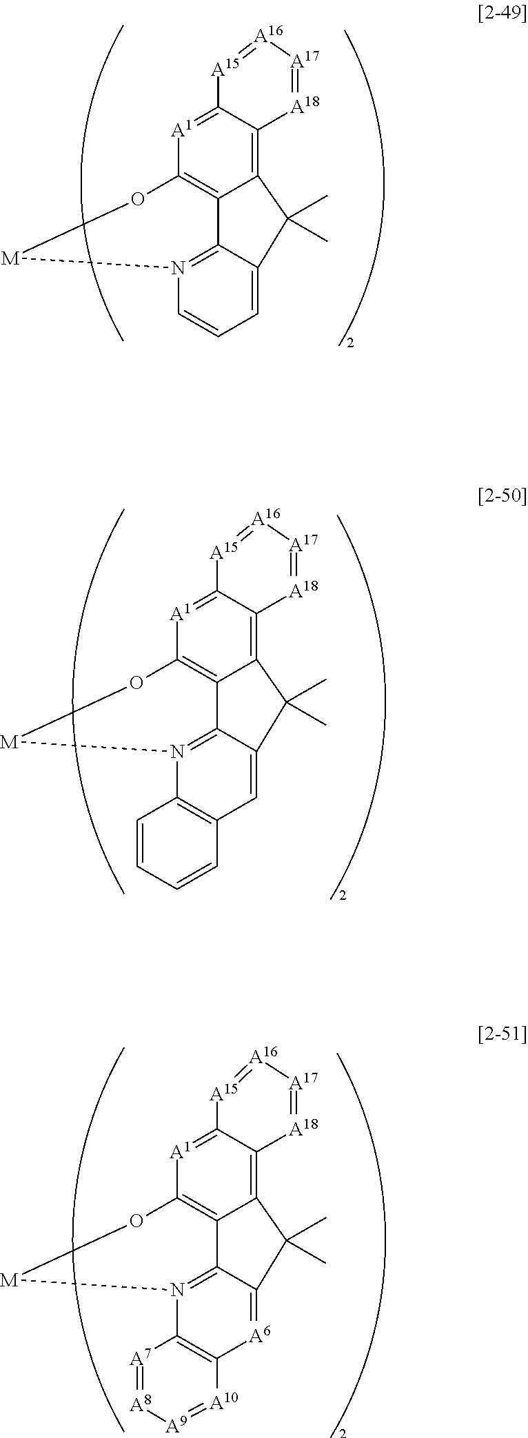


| TABLE 1 | |||||
| Color | Maximum | ||||
| coordinates | emission | ||||
| Voltage | Efficiency | (CIE) | wavelength | ||
| (V) | (cd/A) | x | y | (λmax) (nm) | ||
| Example 2-1 | 5.3 | 42 | 0.330 | 0.612 | 518 |
| Example 2-2 | 4.8 | 39 | 0.327 | 0.611 | 517 |
| Example 2-3 | 4.8 | 38 | 0.328 | 0.613 | 517 |
| Example 2-4 | 5.0 | 35 | 0.325 | 0.615 | 516 |
| Example 2-5 | 5.1 | 35 | 0.326 | 0.614 | 516 |
| Example 2-6 | 5.3 | 41 | 0.328 | 0.611 | 517 |
| Example 2-7 | 5.4 | 40 | 0.331 | 0.613 | 518 |
| Example 2-8 | 5.3 | 39 | 0.330 | 0.613 | 518 |
| Example 2-9 | 5.8 | 34 | 0.329 | 0.613 | 517 |
| Example 2-10 | 5.1 | 37 | 0.329 | 0.612 | 517 |
| Example 2-11 | 4.8 | 40 | 0.327 | 0.611 | 517 |
| Example 2-12 | 5.3 | 35 | 0.326 | 0.615 | 516 |
| Example 2-13 | 5.3 | 36 | 0.330 | 0.613 | 518 |
| Example 2-14 | 5.0 | 34 | 0.326 | 0.615 | 516 |
| Comparative | 6.1 | 33 | 0.327 | 0.611 | 517 |
| Example 2 | |||||
| TABLE 2 | |||||
| Color | Maximum | ||||
| coordinates | emission | ||||
| Voltage | Efficiency | (CIE) | wavelength | ||
| (V) | (cd/A) | x | y | (λmax) (nm) | ||
| Example 3-1 | 5.4 | 20 | 0.661 | 0.338 | 625 |
| Example 3-2 | 4.7 | 23 | 0.663 | 0.337 | 626 |
| Example 3-3 | 4.7 | 24 | 0.662 | 0.338 | 625 |
| Example 3-4 | 4.2 | 29 | 0.660 | 0.340 | 624 |
| Example 3-5 | 4.3 | 30 | 0.661 | 0.339 | 625 |
| Example 3-6 | 4.8 | 23 | 0.661 | 0.338 | 625 |
| Example 3-7 | 4.9 | 22 | 0.660 | 0.340 | 625 |
| Example 3-8 | 5.1 | 21 | 0.662 | 0.338 | 626 |
| Example 3-9 | 4.7 | 26 | 0.660 | 0.340 | 625 |
| Example 3-10 | 4.9 | 25 | 0.662 | 0.337 | 625 |
| Example 3-11 | 4.6 | 27 | 0.660 | 0.340 | 624 |
| Example 3-12 | 5.1 | 23 | 0.662 | 0.338 | 625 |
| Example 3-13 | 5.3 | 21 | 0.661 | 0.339 | 625 |
| Example 3-14 | 4.9 | 24 | 0.660 | 0.340 | 625 |
| Comparative | 5.6 | 19 | 0.661 | 0.338 | 625 |
| Example 3 | |||||
Claims (5)


Priority Applications (1)
| Application Number | Priority Date | Filing Date | Title |
|---|---|---|---|
| US14/814,085 US20150340628A1 (en) | 2010-07-14 | 2015-07-30 | Metal complex compound and organic light emitting diode device including the same |
Applications Claiming Priority (2)
| Application Number | Priority Date | Filing Date | Title |
|---|---|---|---|
| KR10-2010-0068017 | 2010-07-14 | ||
| KR1020100068017A KR101201721B1 (en) | 2010-07-14 | 2010-07-14 | Metal complex compound and organic light emitting diode device including the same |
Related Child Applications (1)
| Application Number | Title | Priority Date | Filing Date |
|---|---|---|---|
| US14/814,085 Continuation US20150340628A1 (en) | 2010-07-14 | 2015-07-30 | Metal complex compound and organic light emitting diode device including the same |
Publications (2)
| Publication Number | Publication Date |
|---|---|
| US20120012824A1 US20120012824A1 (en) | 2012-01-19 |
| US9096529B2 true US9096529B2 (en) | 2015-08-04 |
Family
ID=44720229
Family Applications (2)
| Application Number | Title | Priority Date | Filing Date |
|---|---|---|---|
| US13/168,760 Active 2032-05-02 US9096529B2 (en) | 2010-07-14 | 2011-06-24 | Metal complex compound and organic light emitting diode device including the same |
| US14/814,085 Abandoned US20150340628A1 (en) | 2010-07-14 | 2015-07-30 | Metal complex compound and organic light emitting diode device including the same |
Family Applications After (1)
| Application Number | Title | Priority Date | Filing Date |
|---|---|---|---|
| US14/814,085 Abandoned US20150340628A1 (en) | 2010-07-14 | 2015-07-30 | Metal complex compound and organic light emitting diode device including the same |
Country Status (4)
| Country | Link |
|---|---|
| US (2) | US9096529B2 (en) |
| EP (1) | EP2407458B1 (en) |
| JP (1) | JP5850613B2 (en) |
| KR (1) | KR101201721B1 (en) |
Cited By (1)
| Publication number | Priority date | Publication date | Assignee | Title |
|---|---|---|---|---|
| US10811618B2 (en) | 2016-12-19 | 2020-10-20 | Universal Display Corporation | Organic electroluminescent materials and devices |
Families Citing this family (5)
| Publication number | Priority date | Publication date | Assignee | Title |
|---|---|---|---|---|
| KR102021273B1 (en) * | 2011-05-27 | 2019-09-16 | 가부시키가이샤 한도오따이 에네루기 켄큐쇼 | Carbazole compound, light-emitting element, light-emitting device, electronic device, and lighting device |
| KR101512014B1 (en) | 2012-04-05 | 2015-04-16 | (주)씨에스엘쏠라 | New arylcarbazolylacridine-based organic electroluminescent compounds and organic electroluminescent device comprising the same |
| KR20140071897A (en) | 2012-11-26 | 2014-06-12 | 가부시키가이샤 한도오따이 에네루기 켄큐쇼 | Light-emitting element, light-emitting device, electronic device, and lighting device |
| KR102379123B1 (en) | 2015-08-27 | 2022-03-24 | 엘지디스플레이 주식회사 | Organic light emitting display device and lighting apparatus for vehicles using the same |
| KR102140189B1 (en) * | 2016-07-11 | 2020-07-31 | 엘티소재주식회사 | Hetero-cyclic compound and organic light emitting device using the same |
Citations (8)
| Publication number | Priority date | Publication date | Assignee | Title |
|---|---|---|---|---|
| JPH07197021A (en) | 1994-01-06 | 1995-08-01 | Fuji Electric Co Ltd | Organic thin film light emitting device |
| JPH09176629A (en) | 1995-12-25 | 1997-07-08 | Toyo Ink Mfg Co Ltd | Organic electroluminescent device material and organic electroluminescent device using the same |
| JP2000012222A (en) | 1998-06-19 | 2000-01-14 | Toray Ind Inc | Light-emitting element |
| JP2000100569A (en) | 1998-09-22 | 2000-04-07 | Toray Ind Inc | Luminescent element |
| JP2000208261A (en) | 1999-01-13 | 2000-07-28 | Minolta Co Ltd | Organic electroluminescence element |
| JP2000357588A (en) | 1999-06-11 | 2000-12-26 | Toyota Central Res & Dev Lab Inc | Organic electroluminescent device |
| US20050019605A1 (en) | 2003-07-25 | 2005-01-27 | Raymond Kwong | Materials and structures for enhancing the performance of organic light emitting devices |
| US20070034863A1 (en) * | 2003-09-29 | 2007-02-15 | Rocco Fortte | Metal complexes |
-
2010
- 2010-07-14 KR KR1020100068017A patent/KR101201721B1/en active Active
- 2010-12-16 JP JP2010280380A patent/JP5850613B2/en active Active
-
2011
- 2011-06-24 US US13/168,760 patent/US9096529B2/en active Active
- 2011-07-04 EP EP11172555.2A patent/EP2407458B1/en active Active
-
2015
- 2015-07-30 US US14/814,085 patent/US20150340628A1/en not_active Abandoned
Patent Citations (8)
| Publication number | Priority date | Publication date | Assignee | Title |
|---|---|---|---|---|
| JPH07197021A (en) | 1994-01-06 | 1995-08-01 | Fuji Electric Co Ltd | Organic thin film light emitting device |
| JPH09176629A (en) | 1995-12-25 | 1997-07-08 | Toyo Ink Mfg Co Ltd | Organic electroluminescent device material and organic electroluminescent device using the same |
| JP2000012222A (en) | 1998-06-19 | 2000-01-14 | Toray Ind Inc | Light-emitting element |
| JP2000100569A (en) | 1998-09-22 | 2000-04-07 | Toray Ind Inc | Luminescent element |
| JP2000208261A (en) | 1999-01-13 | 2000-07-28 | Minolta Co Ltd | Organic electroluminescence element |
| JP2000357588A (en) | 1999-06-11 | 2000-12-26 | Toyota Central Res & Dev Lab Inc | Organic electroluminescent device |
| US20050019605A1 (en) | 2003-07-25 | 2005-01-27 | Raymond Kwong | Materials and structures for enhancing the performance of organic light emitting devices |
| US20070034863A1 (en) * | 2003-09-29 | 2007-02-15 | Rocco Fortte | Metal complexes |
Non-Patent Citations (4)
| Title |
|---|
| Extended European Search Report dated Oct. 17, 2011, issued by the European Patent Office, 6 pages. |
| Machine translation of JP09-176629. Date of publication: Jul. 8, 1997. * |
| Machine translation of JP2000-357588. Date of publication: Dec. 26, 2000. * |
| Qiao et al. "High-efficiency organic to near-infrared emissions from bis-cyclometalated iridium complexes with phenyl-benzoquinoline isomers as ligands" J. Mater. Chem. 2009, 19, 6573-6580. Date of publication: Jul. 22, 2009. * |
Cited By (1)
| Publication number | Priority date | Publication date | Assignee | Title |
|---|---|---|---|---|
| US10811618B2 (en) | 2016-12-19 | 2020-10-20 | Universal Display Corporation | Organic electroluminescent materials and devices |
Also Published As
| Publication number | Publication date |
|---|---|
| KR101201721B1 (en) | 2012-11-15 |
| EP2407458B1 (en) | 2014-10-29 |
| EP2407458A1 (en) | 2012-01-18 |
| JP5850613B2 (en) | 2016-02-03 |
| KR20120007312A (en) | 2012-01-20 |
| JP2012020986A (en) | 2012-02-02 |
| US20150340628A1 (en) | 2015-11-26 |
| US20120012824A1 (en) | 2012-01-19 |
Similar Documents
| Publication | Publication Date | Title |
|---|---|---|
| US11515482B2 (en) | Deep HOMO (highest occupied molecular orbital) emitter device structures | |
| US20220220374A1 (en) | Metal-assisted delayed fluorescent materials as co-host materials for fluorescent oleds | |
| US20150340628A1 (en) | Metal complex compound and organic light emitting diode device including the same | |
| US9478748B2 (en) | Organic light emitting diode device | |
| US20230172060A1 (en) | Organic light emitting device | |
| US9105858B2 (en) | Organic electroluminescent device and display apparatus | |
| US8872423B2 (en) | Organic electroluminescent device and display device | |
| US11997919B2 (en) | Organic electric element, display panel comprising the same and display device comprising the same | |
| US11345663B2 (en) | Compound and display panel containing the same | |
| US20250280653A1 (en) | Organic electroluminescent device, organic electroluminescent apparatus and photoelectric device | |
| US10128445B2 (en) | Organic light emitting element and organic light emitting display device including the same | |
| US11889754B2 (en) | Organic compound, and organic light emitting diode and organic light emitting display device including the same | |
| US12167680B2 (en) | Organic electric element, display panel comprising the same and display device comprising the same | |
| US20100140603A1 (en) | Blue light emitting compound and organic light emitting diode device comprising the same | |
| US11411184B2 (en) | Compound, display panel, and display apparatus | |
| US12016242B2 (en) | Heterocyclic compound and application thereof | |
| CN102157703B (en) | OLED (Organic Light Emitting Diode) device for increasing brightness | |
| US11751475B2 (en) | Organic compound, display panel and display apparatus | |
| US20230200209A1 (en) | Organometallic compound and organic light-emitting diode including the same | |
| US12545833B2 (en) | Organic compound, organic light emitting diode, and organic light emitting display device including the same | |
| US20070148494A1 (en) | Display device | |
| US20140332777A1 (en) | Phosphorescent host material and organic light-emitting device including the same | |
| US8835022B2 (en) | Metal complex compound and organic light emitting diode device including the same | |
| US20230209989A1 (en) | Organometallic compound and organic light-emitting diode including the same | |
| US20250098405A1 (en) | Light emitting device and display panel |
Legal Events
| Date | Code | Title | Description |
|---|---|---|---|
| AS | Assignment |
Owner name: SAMSUNG MOBILE DISPLAY CO., LTD., KOREA, REPUBLIC Free format text: ASSIGNMENT OF ASSIGNORS INTEREST;ASSIGNORS:HAMADA, YUJI;LEE, KWAN-HEE;REEL/FRAME:026509/0734 Effective date: 20110620 |
|
| AS | Assignment |
Owner name: SAMSUNG DISPLAY CO., LTD., KOREA, REPUBLIC OF Free format text: MERGER;ASSIGNOR:SAMSUNG MOBILE DISPLAY CO., LTD.;REEL/FRAME:028921/0334 Effective date: 20120702 |
|
| FEPP | Fee payment procedure |
Free format text: PAYOR NUMBER ASSIGNED (ORIGINAL EVENT CODE: ASPN); ENTITY STATUS OF PATENT OWNER: LARGE ENTITY |
|
| FEPP | Fee payment procedure |
Free format text: PAYOR NUMBER ASSIGNED (ORIGINAL EVENT CODE: ASPN); ENTITY STATUS OF PATENT OWNER: LARGE ENTITY |
|
| FEPP | Fee payment procedure |
Free format text: PAYER NUMBER DE-ASSIGNED (ORIGINAL EVENT CODE: RMPN); ENTITY STATUS OF PATENT OWNER: LARGE ENTITY |
|
| STCF | Information on status: patent grant |
Free format text: PATENTED CASE |
|
| MAFP | Maintenance fee payment |
Free format text: PAYMENT OF MAINTENANCE FEE, 4TH YEAR, LARGE ENTITY (ORIGINAL EVENT CODE: M1551); ENTITY STATUS OF PATENT OWNER: LARGE ENTITY Year of fee payment: 4 |
|
| MAFP | Maintenance fee payment |
Free format text: PAYMENT OF MAINTENANCE FEE, 8TH YEAR, LARGE ENTITY (ORIGINAL EVENT CODE: M1552); ENTITY STATUS OF PATENT OWNER: LARGE ENTITY Year of fee payment: 8 |