US11889754B2 - Organic compound, and organic light emitting diode and organic light emitting display device including the same - Google Patents

Organic compound, and organic light emitting diode and organic light emitting display device including the same Download PDF

Info

Publication number
US11889754B2
US11889754B2 US16/985,079 US202016985079A US11889754B2 US 11889754 B2 US11889754 B2 US 11889754B2 US 202016985079 A US202016985079 A US 202016985079A US 11889754 B2 US11889754 B2 US 11889754B2
Authority
US
United States
Prior art keywords
compound
substituted
unsubstituted
mol
light emitting
Prior art date
Legal status (The legal status is an assumption and is not a legal conclusion. Google has not performed a legal analysis and makes no representation as to the accuracy of the status listed.)
Active, expires
Application number
US16/985,079
Other versions
US20210050527A1 (en
Inventor
Ji-Cheol SHIN
Seon-Keun Yoo
Jeong-Dae Seo
Sang-Beom Kim
Hee-Jun Park
Seo-Yong HYUN
Seok-Keun Yoon
Current Assignee (The listed assignees may be inaccurate. Google has not performed a legal analysis and makes no representation or warranty as to the accuracy of the list.)
P & Htech
LG Display Co Ltd
P&H Tech Co Ltd
Original Assignee
P & Htech
LG Display Co Ltd
Priority date (The priority date is an assumption and is not a legal conclusion. Google has not performed a legal analysis and makes no representation as to the accuracy of the date listed.)
Filing date
Publication date
Application filed by P & Htech, LG Display Co Ltd filed Critical P & Htech
Assigned to P&H TECH reassignment P&H TECH ASSIGNMENT OF ASSIGNORS INTEREST (SEE DOCUMENT FOR DETAILS). Assignors: HYUN, Seo-Yong, YOON, SEOK-KEUN
Assigned to LG DISPLAY CO., LTD reassignment LG DISPLAY CO., LTD ASSIGNMENT OF ASSIGNORS INTEREST (SEE DOCUMENT FOR DETAILS). Assignors: KIM, SANG-BEOM, PARK, HEE-JUN, SEO, JEONG-DAE, SHIN, Ji-Cheol, YOO, SEON-KEUN
Assigned to P&H TECH reassignment P&H TECH CORRECTIVE ASSIGNMENT TO CORRECT THE ERROR ON THE COVER SHEET ATTORNEY'S SIGNATURE PREVIOUSLY RECORDED ON REEL 053438 FRAME 0253. ASSIGNOR(S) HEREBY CONFIRMS THE ASSIGNMENT. Assignors: HYUN, Seo-Yong, YOON, SEOK-KEUN
Publication of US20210050527A1 publication Critical patent/US20210050527A1/en
Application granted granted Critical
Publication of US11889754B2 publication Critical patent/US11889754B2/en
Active legal-status Critical Current
Adjusted expiration legal-status Critical

Links

Images

Classifications

    • CCHEMISTRY; METALLURGY
    • C07ORGANIC CHEMISTRY
    • C07DHETEROCYCLIC COMPOUNDS
    • C07D403/00Heterocyclic compounds containing two or more hetero rings, having nitrogen atoms as the only ring hetero atoms, not provided for by group C07D401/00
    • C07D403/02Heterocyclic compounds containing two or more hetero rings, having nitrogen atoms as the only ring hetero atoms, not provided for by group C07D401/00 containing two hetero rings
    • C07D403/04Heterocyclic compounds containing two or more hetero rings, having nitrogen atoms as the only ring hetero atoms, not provided for by group C07D401/00 containing two hetero rings directly linked by a ring-member-to-ring-member bond
    • HELECTRICITY
    • H10SEMICONDUCTOR DEVICES; ELECTRIC SOLID-STATE DEVICES NOT OTHERWISE PROVIDED FOR
    • H10KORGANIC ELECTRIC SOLID-STATE DEVICES
    • H10K85/00Organic materials used in the body or electrodes of devices covered by this subclass
    • H10K85/60Organic compounds having low molecular weight
    • H10K85/649Aromatic compounds comprising a hetero atom
    • H10K85/654Aromatic compounds comprising a hetero atom comprising only nitrogen as heteroatom
    • CCHEMISTRY; METALLURGY
    • C07ORGANIC CHEMISTRY
    • C07DHETEROCYCLIC COMPOUNDS
    • C07D401/00Heterocyclic compounds containing two or more hetero rings, having nitrogen atoms as the only ring hetero atoms, at least one ring being a six-membered ring with only one nitrogen atom
    • C07D401/14Heterocyclic compounds containing two or more hetero rings, having nitrogen atoms as the only ring hetero atoms, at least one ring being a six-membered ring with only one nitrogen atom containing three or more hetero rings
    • CCHEMISTRY; METALLURGY
    • C07ORGANIC CHEMISTRY
    • C07DHETEROCYCLIC COMPOUNDS
    • C07D403/00Heterocyclic compounds containing two or more hetero rings, having nitrogen atoms as the only ring hetero atoms, not provided for by group C07D401/00
    • C07D403/02Heterocyclic compounds containing two or more hetero rings, having nitrogen atoms as the only ring hetero atoms, not provided for by group C07D401/00 containing two hetero rings
    • C07D403/10Heterocyclic compounds containing two or more hetero rings, having nitrogen atoms as the only ring hetero atoms, not provided for by group C07D401/00 containing two hetero rings linked by a carbon chain containing aromatic rings
    • CCHEMISTRY; METALLURGY
    • C07ORGANIC CHEMISTRY
    • C07DHETEROCYCLIC COMPOUNDS
    • C07D403/00Heterocyclic compounds containing two or more hetero rings, having nitrogen atoms as the only ring hetero atoms, not provided for by group C07D401/00
    • C07D403/14Heterocyclic compounds containing two or more hetero rings, having nitrogen atoms as the only ring hetero atoms, not provided for by group C07D401/00 containing three or more hetero rings
    • CCHEMISTRY; METALLURGY
    • C07ORGANIC CHEMISTRY
    • C07DHETEROCYCLIC COMPOUNDS
    • C07D413/00Heterocyclic compounds containing two or more hetero rings, at least one ring having nitrogen and oxygen atoms as the only ring hetero atoms
    • C07D413/02Heterocyclic compounds containing two or more hetero rings, at least one ring having nitrogen and oxygen atoms as the only ring hetero atoms containing two hetero rings
    • C07D413/04Heterocyclic compounds containing two or more hetero rings, at least one ring having nitrogen and oxygen atoms as the only ring hetero atoms containing two hetero rings directly linked by a ring-member-to-ring-member bond
    • CCHEMISTRY; METALLURGY
    • C07ORGANIC CHEMISTRY
    • C07DHETEROCYCLIC COMPOUNDS
    • C07D413/00Heterocyclic compounds containing two or more hetero rings, at least one ring having nitrogen and oxygen atoms as the only ring hetero atoms
    • C07D413/14Heterocyclic compounds containing two or more hetero rings, at least one ring having nitrogen and oxygen atoms as the only ring hetero atoms containing three or more hetero rings
    • CCHEMISTRY; METALLURGY
    • C07ORGANIC CHEMISTRY
    • C07DHETEROCYCLIC COMPOUNDS
    • C07D471/00Heterocyclic compounds containing nitrogen atoms as the only ring hetero atoms in the condensed system, at least one ring being a six-membered ring with one nitrogen atom, not provided for by groups C07D451/00 - C07D463/00
    • C07D471/02Heterocyclic compounds containing nitrogen atoms as the only ring hetero atoms in the condensed system, at least one ring being a six-membered ring with one nitrogen atom, not provided for by groups C07D451/00 - C07D463/00 in which the condensed system contains two hetero rings
    • C07D471/04Ortho-condensed systems
    • CCHEMISTRY; METALLURGY
    • C07ORGANIC CHEMISTRY
    • C07DHETEROCYCLIC COMPOUNDS
    • C07D487/00Heterocyclic compounds containing nitrogen atoms as the only ring hetero atoms in the condensed system, not provided for by groups C07D451/00 - C07D477/00
    • C07D487/02Heterocyclic compounds containing nitrogen atoms as the only ring hetero atoms in the condensed system, not provided for by groups C07D451/00 - C07D477/00 in which the condensed system contains two hetero rings
    • C07D487/04Ortho-condensed systems
    • CCHEMISTRY; METALLURGY
    • C07ORGANIC CHEMISTRY
    • C07DHETEROCYCLIC COMPOUNDS
    • C07D498/00Heterocyclic compounds containing in the condensed system at least one hetero ring having nitrogen and oxygen atoms as the only ring hetero atoms
    • C07D498/02Heterocyclic compounds containing in the condensed system at least one hetero ring having nitrogen and oxygen atoms as the only ring hetero atoms in which the condensed system contains two hetero rings
    • C07D498/04Ortho-condensed systems
    • CCHEMISTRY; METALLURGY
    • C07ORGANIC CHEMISTRY
    • C07DHETEROCYCLIC COMPOUNDS
    • C07D519/00Heterocyclic compounds containing more than one system of two or more relevant hetero rings condensed among themselves or condensed with a common carbocyclic ring system not provided for in groups C07D453/00 or C07D455/00
    • CCHEMISTRY; METALLURGY
    • C09DYES; PAINTS; POLISHES; NATURAL RESINS; ADHESIVES; COMPOSITIONS NOT OTHERWISE PROVIDED FOR; APPLICATIONS OF MATERIALS NOT OTHERWISE PROVIDED FOR
    • C09KMATERIALS FOR MISCELLANEOUS APPLICATIONS, NOT PROVIDED FOR ELSEWHERE
    • C09K11/00Luminescent, e.g. electroluminescent, chemiluminescent materials
    • C09K11/06Luminescent, e.g. electroluminescent, chemiluminescent materials containing organic luminescent materials
    • HELECTRICITY
    • H10SEMICONDUCTOR DEVICES; ELECTRIC SOLID-STATE DEVICES NOT OTHERWISE PROVIDED FOR
    • H10KORGANIC ELECTRIC SOLID-STATE DEVICES
    • H10K50/00Organic light-emitting devices
    • H10K50/10OLEDs or polymer light-emitting diodes [PLED]
    • H10K50/11OLEDs or polymer light-emitting diodes [PLED] characterised by the electroluminescent [EL] layers
    • HELECTRICITY
    • H10SEMICONDUCTOR DEVICES; ELECTRIC SOLID-STATE DEVICES NOT OTHERWISE PROVIDED FOR
    • H10KORGANIC ELECTRIC SOLID-STATE DEVICES
    • H10K50/00Organic light-emitting devices
    • H10K50/10OLEDs or polymer light-emitting diodes [PLED]
    • H10K50/14Carrier transporting layers
    • H10K50/15Hole transporting layers
    • H10K50/155Hole transporting layers comprising dopants
    • HELECTRICITY
    • H10SEMICONDUCTOR DEVICES; ELECTRIC SOLID-STATE DEVICES NOT OTHERWISE PROVIDED FOR
    • H10KORGANIC ELECTRIC SOLID-STATE DEVICES
    • H10K85/00Organic materials used in the body or electrodes of devices covered by this subclass
    • H10K85/60Organic compounds having low molecular weight
    • H10K85/615Polycyclic condensed aromatic hydrocarbons, e.g. anthracene
    • HELECTRICITY
    • H10SEMICONDUCTOR DEVICES; ELECTRIC SOLID-STATE DEVICES NOT OTHERWISE PROVIDED FOR
    • H10KORGANIC ELECTRIC SOLID-STATE DEVICES
    • H10K85/00Organic materials used in the body or electrodes of devices covered by this subclass
    • H10K85/60Organic compounds having low molecular weight
    • H10K85/649Aromatic compounds comprising a hetero atom
    • H10K85/657Polycyclic condensed heteroaromatic hydrocarbons
    • H10K85/6572Polycyclic condensed heteroaromatic hydrocarbons comprising only nitrogen in the heteroaromatic polycondensed ring system, e.g. phenanthroline or carbazole
    • CCHEMISTRY; METALLURGY
    • C09DYES; PAINTS; POLISHES; NATURAL RESINS; ADHESIVES; COMPOSITIONS NOT OTHERWISE PROVIDED FOR; APPLICATIONS OF MATERIALS NOT OTHERWISE PROVIDED FOR
    • C09KMATERIALS FOR MISCELLANEOUS APPLICATIONS, NOT PROVIDED FOR ELSEWHERE
    • C09K2211/00Chemical nature of organic luminescent or tenebrescent compounds
    • C09K2211/10Non-macromolecular compounds
    • C09K2211/1018Heterocyclic compounds
    • HELECTRICITY
    • H10SEMICONDUCTOR DEVICES; ELECTRIC SOLID-STATE DEVICES NOT OTHERWISE PROVIDED FOR
    • H10KORGANIC ELECTRIC SOLID-STATE DEVICES
    • H10K50/00Organic light-emitting devices
    • H10K50/10OLEDs or polymer light-emitting diodes [PLED]
    • H10K50/11OLEDs or polymer light-emitting diodes [PLED] characterised by the electroluminescent [EL] layers
    • H10K50/125OLEDs or polymer light-emitting diodes [PLED] characterised by the electroluminescent [EL] layers specially adapted for multicolour light emission, e.g. for emitting white light
    • H10K50/13OLEDs or polymer light-emitting diodes [PLED] characterised by the electroluminescent [EL] layers specially adapted for multicolour light emission, e.g. for emitting white light comprising stacked EL layers within one EL unit
    • H10K50/131OLEDs or polymer light-emitting diodes [PLED] characterised by the electroluminescent [EL] layers specially adapted for multicolour light emission, e.g. for emitting white light comprising stacked EL layers within one EL unit with spacer layers between the electroluminescent layers
    • HELECTRICITY
    • H10SEMICONDUCTOR DEVICES; ELECTRIC SOLID-STATE DEVICES NOT OTHERWISE PROVIDED FOR
    • H10KORGANIC ELECTRIC SOLID-STATE DEVICES
    • H10K50/00Organic light-emitting devices
    • H10K50/10OLEDs or polymer light-emitting diodes [PLED]
    • H10K50/14Carrier transporting layers
    • H10K50/15Hole transporting layers
    • HELECTRICITY
    • H10SEMICONDUCTOR DEVICES; ELECTRIC SOLID-STATE DEVICES NOT OTHERWISE PROVIDED FOR
    • H10KORGANIC ELECTRIC SOLID-STATE DEVICES
    • H10K50/00Organic light-emitting devices
    • H10K50/10OLEDs or polymer light-emitting diodes [PLED]
    • H10K50/17Carrier injection layers
    • H10K50/171Electron injection layers
    • HELECTRICITY
    • H10SEMICONDUCTOR DEVICES; ELECTRIC SOLID-STATE DEVICES NOT OTHERWISE PROVIDED FOR
    • H10KORGANIC ELECTRIC SOLID-STATE DEVICES
    • H10K59/00Integrated devices, or assemblies of multiple devices, comprising at least one organic light-emitting element covered by group H10K50/00
    • H10K59/10OLED displays
    • H10K59/12Active-matrix OLED [AMOLED] displays
    • HELECTRICITY
    • H10SEMICONDUCTOR DEVICES; ELECTRIC SOLID-STATE DEVICES NOT OTHERWISE PROVIDED FOR
    • H10KORGANIC ELECTRIC SOLID-STATE DEVICES
    • H10K59/00Integrated devices, or assemblies of multiple devices, comprising at least one organic light-emitting element covered by group H10K50/00
    • H10K59/30Devices specially adapted for multicolour light emission
    • H10K59/38Devices specially adapted for multicolour light emission comprising colour filters or colour changing media [CCM]

Definitions

  • the present disclosure relates to an organic compound, and more particularly, to an organic compound being capable of increasing an emitting efficiency and decreasing a driving voltage, and an organic light emitting diode and an organic light emitting display (OLED) device including the organic compound.
  • organic compound being capable of increasing an emitting efficiency and decreasing a driving voltage
  • organic light emitting diode and an organic light emitting display (OLED) device including the organic compound.
  • OLED device which includes an organic light emitting diode and may be called to as an organic electroluminescent device
  • the organic light emitting diode emits light by injecting electrons from a cathode as an electron injection electrode and holes from an anode as a hole injection electrode into an organic emitting layer, combining the electrons with the holes, generating an exciton, and transforming the exciton from an excited state to a ground state.
  • a flexible transparent substrate for example, a plastic substrate, can be used as a base substrate where elements are formed.
  • the organic light emitting diode can be operated at a voltage lower than a voltage required to operate other display devices and has low power consumption.
  • the light from the organic light emitting diode has excellent color purity.
  • the organic emitting layer may has a multi-layered structure having a hole injection layer (HIL), a hole transporting layer (HTL), an emitting material layer (EML), an electron transporting layer (ETL) and an electron injection layer (EIL).
  • HIL hole injection layer
  • HTL hole transporting layer
  • EML emitting material layer
  • ETL electron transporting layer
  • EIL electron injection layer
  • the organic light emitting diode there is a limitation in a hole injection/transporting property into the EML. As a result, the organic light emitting diode and the OLED device have low emitting efficiency and high driving voltage.
  • the present disclosure is directed to an organic compound, an organic light emitting diode and an OLED device that substantially obviate one or more of the problems associated with the limitations and disadvantages of the related conventional art.
  • an aspect of the present disclosure is an organic compound of Formula 1:
  • each of X 1 , X 2 and X 3 is independently selected from carbon (C) and nitrogen (N), provided that at least one of X 1 to X 3 is N; each of Z 1 , Z 2 and Z 3 is independently selected from a substituted or unsubstituted C6 to C30 aryl group, a substituted or unsubstituted C5 to C30 heteroaryl group, a substituted or unsubstituted C1 to C12 alkyl group, a substituted or unsubstituted C1 to C12 alkoxy group, a substituted or unsubstituted C1 to C12 ether group, halogen, cyano (CN), and trimethylsilyl; or each of Z 1 , Z 2 and Z 3 is represented by one of the following Formula 2, Formula 3 and Formula 4, provided that at least one of Z1 to Z3 is selected from one of the Formulas 2 to 4,
  • each of X 11 and X 12 is independently selected from C and N, provided that at least one of X 11 and X 12 is N; each of X 13 to X 16 is independently selected from C and N; R 1 is selected from a substituted or unsubstituted C6 to C30 aryl group, a substituted or unsubstituted C5 to C30 heteroaryl group, a substituted or unsubstituted C1 to C12 alkyl group, a substituted or unsubstituted C1 to C12 alkoxy group, cyano, halogen and trifluoromethyl; and m1 is an integer of 0 to 4.
  • each of X 2 and X 22 is independently selected from C and N, provided that at least one of X 21 and X 22 is N;
  • R 2 is selected from cyano and phenyl;
  • R 3 is selected from a substituted or unsubstituted C6 to C30 aryl group, a substituted or unsubstituted C5 to C30 heteroaryl group, a substituted or unsubstituted C1 to C12 alkyl group, a substituted or unsubstituted C1 to C12 alkoxy group, cyano, halogen and trifluoromethyl;
  • m2 is an integer of 0 to 3.
  • each of X 31 and X 32 is independently selected from N and oxygen (O), provided that when one of X 31 and X 32 is N, then the other one of X 31 and X 32 is O; each of X 33 to X 36 is independently selected from C and N; R 4 is selected from a substituted or unsubstituted C6 to C30 aryl group, a substituted or unsubstituted C5 to C30 heteroaryl group, a substituted or unsubstituted C1 to C12 alkyl group, a substituted or unsubstituted C1 to C12 alkoxy group, cyano, halogen and trifluoromethyl; and m3 is an integer of 0 to 4.
  • an organic light emitting diode including first and second electrodes facing each other; a first emitting material layer between the first and second electrodes; a first hole auxiliary layer between the first electrode and the first emitting material layer; and a first electron auxiliary layer between the first emitting material layer and the second electrode, wherein the first hole auxiliary layer include a first host and an organic compound of the present disclosure as a first dopant.
  • an organic light emitting diode including first and second electrodes facing each other; a first charge generation layer positioned between the first and second electrodes and including a first N-type charge generation layer and a first P-type charge generation layer; a first emitting stack including a first emitting material layer between the first electrode and the first N-type charge generation layer, a first hole auxiliary layer between the first electrode and the first emitting material layer, and a first electron auxiliary layer between the first emitting material layer and the first N-type charge generation layer; and a second emitting stack including a second emitting material layer between the first P-type charge generation layer and the second electrode, a second hole auxiliary layer between the first P-type charge generation layer and the second emitting material layer, and a second electron auxiliary layer between the second emitting material layer and the second electrode, wherein the first P-type charge generation layer includes a first host and an organic compound of the present disclosure as a first dopant.
  • an organic light emitting display device including a substrate; an organic light emitting diode disposed on or over the substrate; and a thin film transistor positioned between the substrate and the organic light emitting diode and connected to the organic light emitting diode.
  • FIG. 1 is a schematic circuit diagram of an OLED device of the present disclosure.
  • FIG. 2 is a schematic cross-sectional view of an OLED device according to a first embodiment of the present disclosure.
  • FIG. 3 is a schematic cross-sectional view of an organic light emitting diode included in the OLED device according to the first embodiment of the present disclosure.
  • FIG. 4 is a schematic cross-sectional view of an OLED device according to a second embodiment of the present disclosure.
  • FIG. 5 is a schematic cross-sectional view of an OLED device according to a third embodiment of the present disclosure.
  • FIG. 6 is a schematic cross-sectional view of an organic light emitting diode having a two-stack structure included in the OLED device according to the second and third embodiments of the present disclosure.
  • FIG. 7 is a schematic cross-sectional view of an organic light emitting diode having a three-stack structure included in the OLED device according to the second and third embodiments of the present disclosure.
  • FIG. 1 is a schematic circuit diagram of an OLED device of the present disclosure.
  • an OLED device includes a gate line GL, a data line DL, a power line PL, a switching thin film transistor TFT Ts, a driving TFT Td, a storage capacitor Cst, and an organic light emitting diode D.
  • the gate line GL and the data line DL cross each other to define a pixel region P.
  • the switching TFT Ts is connected to the gate line GL and the data line DL, and the driving TFT Td and the storage capacitor Cst are connected to the switching TFT Ts and the power line PL.
  • the organic light emitting diode D is connected to the driving TFT Td.
  • the switching TFT Ts when the switching TFT Ts is turned on by a gate signal applied through the gate line GL, a data signal from the data line DL is applied to the gate electrode of the driving TFT Td and an electrode of the storage capacitor Cst.
  • the driving TFT Td When the driving TFT Td is turned on by the data signal, an electric current is supplied to the organic light emitting diode D from the power line PL. As a result, the organic light emitting diode D emits light. In this case, when the driving TFT Td is turned on, a level of an electric current applied from the power line PL to the organic light emitting diode D is determined such that the organic light emitting diode D can produce a gray scale.
  • the storage capacitor Cst serves to maintain the voltage of the gate electrode of the driving TFT Td when the switching TFT Ts is turned off. Accordingly, even if the switching TFT Ts is turned off, a level of an electric current applied from the power line PL to the organic light emitting diode D is maintained to next frame.
  • the OLED device displays a desired image.
  • FIG. 2 is a schematic cross-sectional view of an OLED device according to a first embodiment of the present disclosure.
  • the OLED device 100 includes a substrate 110 , a driving TFT Td and an organic light emitting diode D connected to the driving TFT Td.
  • the substrate 110 may be a glass substrate or a plastic substrate.
  • the substrate 110 may be a polyimide substrate.
  • a buffer layer 120 is formed on the substrate, and the driving TFT Td is formed on the buffer layer 120 .
  • the buffer layer 120 may be omitted.
  • a semiconductor layer 122 is formed on the buffer layer 120 .
  • the semiconductor layer 122 may include an oxide semiconductor material or polycrystalline silicon.
  • a light-shielding pattern (not shown) may be formed under the semiconductor layer 122 .
  • the light to the semiconductor layer 122 is shielded or blocked by the light-shielding pattern such that thermal degradation of the semiconductor layer 122 can be prevented.
  • impurities may be doped into both sides of the semiconductor layer 122 .
  • a gate insulating layer 124 is formed on the semiconductor layer 122 .
  • the gate insulating layer 124 may be formed of an inorganic insulating material such as silicon oxide or silicon nitride.
  • a gate electrode 130 which is formed of a conductive material, e.g., metal, is formed on the gate insulating layer 124 to correspond to a center of the semiconductor layer 122 .
  • the gate insulating layer 124 is formed on an entire surface of the substrate 110 .
  • the gate insulating layer 124 may be patterned to have the same shape as the gate electrode 130 .
  • An interlayer insulating layer 132 which is formed of an insulating material, is formed on the gate electrode 130 .
  • the interlayer insulating layer 132 may be formed of an inorganic insulating material, e.g., silicon oxide or silicon nitride, or an organic insulating material, e.g., benzocyclobutene or photo-acryl.
  • the interlayer insulating layer 132 includes first and second contact holes 134 and 136 exposing both sides of the semiconductor layer 122 .
  • the first and second contact holes 134 and 136 are positioned at both sides of the gate electrode 130 to be spaced apart from the gate electrode 130 .
  • the first and second contact holes 134 and 136 are formed through the gate insulating layer 124 .
  • the gate insulating layer 124 is patterned to have the same shape as the gate electrode 130 , the first and second contact holes 134 and 136 is formed only through the interlayer insulating layer 132 .
  • a source electrode 140 and a drain electrode 142 which are formed of a conductive material, e.g., metal, are formed on the interlayer insulating layer 132 .
  • the source electrode 140 and the drain electrode 142 are spaced apart from each other with respect to the gate electrode 130 and respectively contact both sides of the semiconductor layer 122 through the first and second contact holes 134 and 136 .
  • the semiconductor layer 122 , the gate electrode 130 , the source electrode 140 and the drain electrode 142 constitute the driving TFT Td.
  • the gate electrode 130 , the source electrode 140 , and the drain electrode 142 are positioned over the semiconductor layer 122 .
  • the driving TFT Td has a coplanar structure.
  • the gate electrode may be positioned under the semiconductor layer, and the source and drain electrodes may be positioned over the semiconductor layer such that the driving TFT Td may have an inverted staggered structure.
  • the semiconductor layer may include amorphous silicon.
  • the gate line and the data line cross each other to define the pixel region, and the switching TFT Ts ( FIG. 1 ) is formed to be connected to the gate and data lines.
  • the switching TFT Ts is connected to the driving TFT Td as the driving element.
  • the power line which may be formed to be parallel to and spaced apart from one of the gate and data lines, and the storage capacitor for maintaining the voltage of the gate electrode of the driving TFT Td in one frame may be further formed.
  • a passivation layer 150 which includes a drain contact hole 152 exposing the drain electrode 142 of the driving TFT Td, is formed to cover the driving TFT Td.
  • a first electrode 160 which is connected to the drain electrode 142 of the driving TFT Td through the drain contact hole 152 , is separately formed in each pixel region.
  • the first electrode 160 may be an anode and may be formed of a conductive material having a relatively high work function.
  • the first electrode 160 may be formed of a transparent conductive material such as indium-tin-oxide (ITO) or indium-zinc-oxide (IZO).
  • a reflection electrode or a reflection layer may be formed under the first electrode 160 .
  • the reflection electrode or the reflection layer may be formed of aluminum-palladium-copper (APC) alloy.
  • a bank layer 166 is formed on the passivation layer 150 to cover an edge of the first electrode 160 .
  • the bank layer 166 is positioned at a boundary of the pixel region and exposes a center of the first electrode 160 in the pixel region.
  • An organic emitting layer 170 is formed on the first electrode 160 .
  • the organic emitting layer 170 is formed in each pixel region P.
  • the organic emitting layer 170 may include a red organic emitting layer, a green organic emitting layer and a blue organic emitting layer in red, green and blue pixel regions, respectively.
  • a second electrode 180 is formed over the substrate 110 where the organic emitting layer 170 is formed.
  • the second electrode 180 covers an entire surface of the display area and may be formed of a conductive material having a relatively low work function to serve as a cathode.
  • the second electrode 180 may be formed of aluminum (Al), magnesium (Mg) or Al—Mg alloy.
  • the first electrode 160 , the organic emitting layer 170 and the second electrode 180 constitute the organic light emitting diode D.
  • an encapsulation film is formed on the second electrode 180 to prevent penetration of moisture into the organic light emitting diode D.
  • the encapsulation film includes a first inorganic insulating layer, an organic insulating layer and a second inorganic insulating layer sequentially stacked, but it is not limited thereto.
  • a polarization plate (not shown) for reducing an ambient light reflection may be disposed over the top-emission type organic light emitting diode D.
  • the polarization plate may be a circular polarization plate.
  • FIG. 3 is a schematic cross-sectional view of an organic light emitting diode included in the OLED device according to the first embodiment of the present disclosure.
  • the organic light emitting diode D includes the first and second electrodes 160 and 180 , which face each other, and the organic emitting layer 170 therebetween.
  • the organic emitting layer 170 includes an emitting material layer (EML) 177 , a hole auxiliary layer 175 between the first electrode 160 and the EML 177 , and an electron auxiliary layer 179 between the EML 177 and the second electrode 180 .
  • EML emitting material layer
  • the hole auxiliary layer 175 includes a host and a dopant of an organic compound of the present disclosure.
  • the hole auxiliary layer 175 may include a hole injection layer (HIL) 171 and a hole transporting layer (HTL) 173 between the HIL 171 and the EML 177 , and the organic compound of the present disclosure as the dopant 190 may be included in the HIL 171 .
  • HIL hole injection layer
  • HTL hole transporting layer
  • the organic compound of the present disclosure which is used as a dopant in the hole auxiliary layer and/or a p-type charge generation layer, is represented by Formula 1.
  • each of X 1 , X 2 and X 3 is independently selected from carbon (C) and nitrogen (N), and at least one of X 1 to X 3 is N.
  • Each of Z 1 , Z 2 and Z 3 is independently selected from a substituted or unsubstituted C6 to C30 aryl group, a substituted or unsubstituted C5 to C30 heteroaryl group, a substituted or unsubstituted C1 to C12 alkyl group, a substituted or unsubstituted C1 to C12 alkoxy group, a substituted or unsubstituted C1 to C12 ether group, halogen, cyano (CN) and trimethylsilyl; or each of X 1 , X 2 and X 3 is independently selected from Formula 2, Formula 3 and Formula 4, and at least one of Z 1 to Z 3 is selected from Formulas 2 to 4.
  • the alkyl group and/or the alkoxy group may be substituted by halogen.
  • a substituted alkyl group may be trifluoromethyl, and a substituted alkoxy group may be trifluoromethoxy.
  • each of X 11 and X 12 is independently selected from C and N, and at least one of X 11 and X 12 is N.
  • Each of X 13 to X 16 is independently selected from C and N.
  • R 1 is selected from a substituted or unsubstituted C6 to C30 aryl group, a substituted or unsubstituted C5 to C30 heteroaryl group, a substituted or unsubstituted C1 to C12 alkyl group, a substituted or unsubstituted C1 to C12 alkoxy group, cyano, halogen and trifluoromethyl, and m1 is an integer of 0 to 4.
  • At least one of X 13 to X 16 may be C, and R 1 may be selected from methyl, trifluoromethyl, trifluoromethoxy, cyano and fluorine (F).
  • each of X 21 and X 22 is independently selected from C and N, and at least one of X 21 and X 22 is N.
  • R 2 is selected from cyano and phenyl
  • R 3 is selected from a substituted or unsubstituted C6 to C30 aryl group, a substituted or unsubstituted C5 to C30 heteroaryl group, a substituted or unsubstituted C1 to C12 alkyl group, a substituted or unsubstituted C1 to C12 alkoxy group, cyano, halogen and trifluoromethyl
  • m2 is an integer of 0 to 3.
  • R 2 may be phenyl substituted by at least one of F and CN, and R 3 may be CN.
  • one of X 31 and X 32 is N, and one of X 31 and X 32 is oxygen (O).
  • Each of X 33 to X 36 is independently selected from C and N.
  • R 4 is selected from a substituted or unsubstituted C6 to C30 aryl group, a substituted or unsubstituted C5 to C30 heteroaryl group, a substituted or unsubstituted C1 to C12 alkyl group, a substituted or unsubstituted C1 to C12 alkoxy group, cyano, halogen and trifluoromethyl, and m3 is an integer of 0 to 4.
  • At least one of X 33 to X 36 may be C, and R 4 may be selected from F, CN and trifluoromethyl.
  • the organic compound of the present disclosure may be one of compounds of Formula 5.
  • the HIL 171 has a first thickness
  • the HTL 173 may have a second thickness being greater than the first thickness.
  • the first thickness may be about 1 to 50 nm
  • the second thickness may be about 50 to 150 nm.
  • a host of the HIL 171 may be the same as or different from a material of the HTL 173 .
  • the host of the HIL 171 and the material of the HTL 173 may be independently selected from the group consisting of NPD (or NPB, N,N′-bis(naphthalen-1-yl)-N,N′-bis(phenyl)-2,2′-dimethylbenzidine), TPD (N,N′-bis-(3-methylphenyl)-N,N′-bis-(phenyl)-benzidine), spiro-TAD (2,2′,7,7′-tetrakis(N,N-diphenylamino)-9,9′-spirofluorene) and MTDATA (4,4′,4′′-tris(N-3-methylphenyl-N-phenylamino)-triphenylamine), but it is not limited thereto.
  • the dopant 190 may have a volume ratio of about 1 to 30 with respect to the host
  • the EML 177 includes a host and a dopant.
  • each of the host and the dopant may be a fluorescent compound, a phosphorescent compound or a delayed fluorescent compound.
  • the electron auxiliary layer 179 may include an electron transporting layer (ETL) and an electron injection layer (EIL) between the ETL and the second electrode 180 .
  • ETL electron transporting layer
  • EIL electron injection layer
  • an electron blocking layer (EBL) may be formed between the hole auxiliary layer 175 and the EML 177
  • a hole blocking layer (HBL) may be formed between the EML 177 and the electron auxiliary layer 179 .
  • the hole auxiliary layer 175 e.g., the HIL 171
  • the hole auxiliary layer 175 includes the host and the organic compound of the present disclosure as the dopant 190 .
  • the LUMO level of the organic compound is equal to or has relatively small difference from the HOMO level of a material in adjacent layer, e.g., the HTL 173 , the hole injection property is improved.
  • a difference between the LUMO level of the organic compound and the HOMO level of the host may be about 0.1 eV or less.
  • the HTL 173 may be formed of the same material as the host of the HIL 171 without the dopant.
  • the organic light emitting diode D and the OLED device 100 including the organic compound as the dopant in the hole auxiliary layer 175 have advantages in the emitting efficiency and the driving voltage.
  • An ITO transparent electrode having an emitting area of 2 mm*2 mm is formed on a glass substrate and is cleaned. In the vacuum chamber of about 10-6 Torr, layers are sequentially deposited on an ITO transparent electrode.
  • HIL host (Formula 6)+p-type dopant (5 vol %), 5 nm), (2) HTL (Formula 6, 100 nm), (3) EBL (Formula 7, 10 nm), (4) EML (host (Formula 8)+dopant (Formula 9, 3 vol %) 20 nm)), (5) ETL (Formula 10+Liq (50 vol %), 30 nm), (6) EIL (LiF, mm), and (7) Cathode (Al, 100 nm)
  • the HIL is formed without the p-type dopant.
  • the properties, i.e., the driving voltage, the emitting efficiency and the color coordinate index, of the organic light emitting diodes of Examples 1 to 37 and Comparative Example are measured using Source meter (Model 237, Keithley) and Luminance meter (PR-650, Photo Research) and listed in Table 1.
  • the driving voltage means a voltage with a current density of 10 mA/cm 2 .
  • the emitting efficiency of the organic light emitting diodes of Ex1 to Ex37 using the organic compounds of the present disclosure as the p-type dopant in the HIL is significantly increased.
  • the driving voltage of the organic light emitting diode of the present disclosure is significantly reduced.
  • FIG. 4 is a schematic cross-sectional view of an OLED device according to a second embodiment of the present disclosure.
  • the OLED device 200 includes a substrate 210 , an emitting diode D over the substrate 210 , a driving TFT Td, which is positioned between the substrate 210 and the organic light emitting diode D and connected to the organic light emitting diode D, and a color filter 230 between the substrate 210 and the organic light emitting diode D.
  • the substrate 210 may be a glass substrate or a plastic substrate.
  • the substrate 210 may be a polyimide substrate.
  • a red pixel region RP, a green pixel region GP and a blue pixel region BP are defined on the substrate 210 , and the driving TFT Td is disposed in each of the red, green and blue pixel regions RP, GP and BP.
  • a white pixel region (not shown) may be further defined on the substrate 210 . In this instance, the driving TFT Td is also disposed in the white pixel region.
  • the driving TFT Td may include a semiconductor layer on the substrate 210 , a gate electrode, which is disposed over the semiconductor layer and overlaps the semiconductor layer, a source electrode, which is disposed over the gate electrode and connected one end of the semiconductor layer, and a drain electrode, which is disposed over the gate electrode and connected to the other end of the semiconductor layer.
  • the source and drain electrodes are spaced apart from each other.
  • a first insulating layer 220 is formed on the driving TFT Td, and the color filter 230 is formed on the first insulating layer 220 .
  • the color filter 230 includes a red color filter pattern 230 a corresponding to the red pixel region RP, a green color filter pattern 230 b corresponding to the green pixel region GP and a blue color filter pattern 230 c corresponding to the blue pixel region BP.
  • a second insulating layer 240 is formed on the color filter 230 .
  • a contact hole 222 which exposes an electrode, e.g., the drain electrode, of the driving TFT Td, is formed through the first and second insulating layers 220 and 240 .
  • the color filter 230 is positioned between the first and second insulating layers 220 and 240 such that the first and second insulating layers 220 and 240 are spaced apart from each other in an emission area of the red, green and blue pixel regions RP, GP and BP.
  • the white pixel regions is further defined, there is no color filter in the white pixel region such that the first and second insulating layers 220 and 240 contact each other in an entire of the white pixel region.
  • a first electrode 250 which is connected to the driving TFT Td through the contact hole 222 , is formed on the second insulating layer 240 .
  • the first electrode 250 is separated in each of the red, green and blue pixel regions RP, GP and BP.
  • the first electrode 250 may serve as an anode and include a conductive material having relatively high work function.
  • the first electrode 250 may be formed or include a transparent conductive material such as indium-tin-oxide (ITO), indium-zinc-oxide (IZO) or zinc oxide (ZnO).
  • a bank layer 260 covering an edge of the first electrode 250 is formed on the second insulating layer 240 .
  • the bank layer 260 exposes a center of the first electrode 250 in the red, green and blue pixel regions RP, GP and BP.
  • An organic emitting layer 252 is formed on the first electrode 250 .
  • the organic emitting layer 252 emits white light and is continuously formed on an entire display area, which include the red, green and blue pixel regions RP, GP and BP, as one body. Namely, the organic emitting layer 252 is formed to cover an entire surface of the bank layer 260 such that the organic emitting layer 252 in adjacent pixel regions is continuous.
  • a second electrode 254 is formed over the substrate 210 including the organic emitting layer 252 .
  • the second electrode 254 covers an entire display area.
  • the second electrode 254 may be formed of or include a conductive material having relatively low work function to serve as a cathode.
  • the second electrode 254 may be formed of aluminum (Al), magnesium (Mg) or Al—Mg alloy.
  • the first electrode 250 , the organic emitting layer 252 and the second electrode 254 constitute the organic light emitting diode D.
  • an encapsulation film may be formed on the second electrode 254 to prevent penetration of moisture into the organic light emitting diode D.
  • the encapsulation film may include a first inorganic insulating layer, an organic insulating layer and a second inorganic insulating layer sequentially stacked, but it is not limited thereto.
  • a polarization plate for reducing an ambient light reflection may be disposed at an outer side of the substrate 210 .
  • the polarization plate may be a circular polarization plate.
  • a cover window (not shown) may be attached on an outer side of the substrate 210 or the polarization plate.
  • the substrate 210 and the cover window may have flexibility such that a flexible OLED device may be provided.
  • the OLED device of FIG. 4 is a bottom-emission type. Namely, the light from the organic emitting layer 252 passes through the first electrode 250 and the color filter 230 such that an image is displayed on a side of the substrate 210 .
  • the first electrode 250 is a transparent electrode
  • the second electrode 254 is a reflective electrode.
  • the light from the organic emitting layer 252 may directly pass through the first electrode 250 or indirectly pass through the first electrode 250 after being reflected on the second electrode 254 .
  • the color filter 230 is positioned between the first and second insulating layers 220 and 240 .
  • a position of the color filter 230 is not restricted thereto in a space between the organic light emitting diode D and the substrate 210 .
  • the color filter 230 may be positioned between the substrate 210 and the first insulating layer 220 .
  • the second insulating layer 240 may be omitted.
  • the OLED device 200 Since the white light from the organic light emitting diode D passes through the color filter 230 , the OLED device 200 displays a full color image.
  • FIG. 5 is a schematic cross-sectional view of an OLED device according to a third embodiment of the present disclosure.
  • the OLED device 200 includes a first substrate 210 , a second electrode 270 facing the first electrode 210 , an organic light emitting diode D over the first substrate 210 , a driving TFT Td, which is positioned between the first substrate 210 and the organic light emitting diode D and connected to the organic light emitting diode D, and a color filter 230 between the second substrate 270 and the organic light emitting diode D.
  • Each of the first and second substrates 210 and 270 may be a glass substrate or a plastic substrate.
  • each of the first and second substrates 210 and 270 may be a polyimide substrate.
  • a red pixel region RP, a green pixel region GP and a blue pixel region BP are defined on the first substrate 210 , and the driving TFT Td is disposed in each of the red, green and blue pixel regions RP, GP and BP.
  • a white pixel region (not shown) may be further defined on the first substrate 210 . In this instance, the driving TFT Td is also disposed in the white pixel region.
  • the driving TFT Td may include a semiconductor layer on the first substrate 210 , a gate electrode, which is disposed over the semiconductor layer and overlaps the semiconductor layer, a source electrode, which is disposed over the gate electrode and connected one end of the semiconductor layer, and a drain electrode, which is disposed over the gate electrode and connected to the other end of the semiconductor layer.
  • the source and drain electrodes are spaced apart from each other.
  • An insulating layer 220 is formed on the driving TFT Td, and a contact hole 222 , which exposes an electrode, e.g., the drain electrode, of the driving TFT Td, is formed through the insulating layer 220 .
  • a first electrode 250 which is connected to the driving TFT Td through the contact hole 222 , is formed on the insulating layer 220 .
  • the first electrode 250 is separated in each of the red, green and blue pixel regions RP, GP and BP.
  • the first electrode 250 may serve as an anode and include a conductive material having relatively high work function.
  • the first electrode 250 may include a transparent electrode layer, which may be formed or include a transparent conductive material such as indium-tin-oxide (ITO), indium-zinc-oxide (IZO) or zinc oxide (ZnO), and a reflection electrode layer (or reflection layer).
  • the first electrode 250 may have a triple-layered structure of upper and lower layers of ITO and a middle layer of aluminum-palladium-copper (APC) alloy.
  • a bank layer 260 covering an edge of the first electrode 250 is formed on the insulating layer 220 .
  • the bank layer 260 exposes a center of the first electrode 250 in the red, green and blue pixel regions RP, GP and BP.
  • An organic emitting layer 252 is formed on the first electrode 250 .
  • the organic emitting layer 252 emits white light and is continuously formed on an entire display area, which include the red, green and blue pixel regions RP, GP and BP, as one body. Namely, the organic emitting layer 252 is formed to cover an entire surface of the bank layer 260 such that the organic emitting layer 252 in adjacent pixel regions is continuous.
  • a second electrode 254 is formed over the substrate 210 including the organic emitting layer 252 .
  • the second electrode 254 covers an entire display area.
  • the second electrode 254 may be formed of or include a conductive material having relatively low work function to serve as a cathode.
  • the second electrode 254 may be formed of aluminum (Al), magnesium (Mg) or Al—Mg alloy and may have a thin profile to transmit the light.
  • the first electrode 250 , the organic emitting layer 252 and the second electrode 254 constitute the organic light emitting diode D.
  • a color filter 230 is formed over the organic light emitting diode D. Namely, the color filter 230 is positioned between the organic light emitting diode D and the second substrate 270 .
  • the color filter 230 includes a red color filter pattern 230 a corresponding to the red pixel region RP, a green color filter pattern 230 b corresponding to the green pixel region GP and a blue color filter pattern 230 c corresponding to the blue pixel region BP.
  • a polarization plate for reducing an ambient light reflection may be disposed at an outer side of the second substrate 270 .
  • the polarization plate may be a circular polarization plate.
  • the OLED device of FIG. 5 is a top-emission type. Namely, the light from the organic emitting layer 252 passes through the second electrode 254 and the color filter 230 such that an image is displayed on a side of the second substrate 270 .
  • the first electrode 250 is a reflective electrode
  • the second electrode 254 is a transparent (semi-transparent) electrode.
  • the light from the organic emitting layer 252 may directly pass through the second electrode 254 or indirectly pass through the second electrode 254 after being reflected on the first electrode 250 .
  • the OLED device 200 Since the white light from the organic light emitting diode D passes through the color filter 230 , the OLED device 200 displays a full color image.
  • FIG. 6 is a schematic cross-sectional view of an organic light emitting diode having a two-stack structure included in the OLED device according to the second and third embodiments of the present disclosure.
  • the emitting diode D includes a first electrode 250 , a second electrode 254 facing the first electrode 250 and an organic emitting layer 252 between the first and second electrodes 250 and 254 , and the organic emitting layer 252 includes first and second emitting stacks ST 1 and ST 2 and a charge generation layer (CGL) 330 .
  • CGL charge generation layer
  • the first electrode 250 may serve as an anode for injecting the hole and may include a conductive material having high work function, e.g., ITO, IZO or ZnO.
  • the second electrode 254 may serve as a cathode for injecting the electron and may include a conductive material having low work function, e.g., Al, Mg or Al—Mg alloy.
  • the second electrode 254 serves as a reflection electrode.
  • the first electrode 250 may further include a reflection layer or a reflection electrode, and the second electrode 254 serves as a transparent electrode.
  • the CGL 330 is positioned between the first and second emitting stacks ST 1 and ST 2 , and the first emitting stack ST 1 , the CGL 330 and the second emitting stack ST 2 are sequentially stacked on the first electrode 250 .
  • the first emitting stack ST 1 is positioned between the first electrode 250 and the CGL 330
  • the second emitting stack ST 2 is positioned between the second electrode 254 and the CGL 330 .
  • the first emitting stack ST 1 which is positioned between the first electrode 250 and the CGL 330 , may include a first EML 316 , a first hole auxiliary layer 313 between the first electrode 250 and the first EML 316 , and a first electron auxiliary layer 318 between the first EML 316 and the CGL 330 .
  • the first hole auxiliary layer 313 may include an HIL 312 and a first HTL 314 between the HIL 312 and the first EML 316 .
  • the first electron auxiliary layer 318 may be a first ETL.
  • the second emitting stack ST 2 may include a second EML 324 between the CGL 330 and the second electrode 254 , a second hole auxiliary layer 322 between the CGL 330 and the second EML 324 , and a second electron auxiliary layer 327 between the second EML 324 and the second electrode 254 .
  • the second hole auxiliary layer 322 may be a second HTL.
  • the second electron auxiliary layer 327 may include a second ETL 326 and an EIL 328 between the second ETL 326 and the second electrode 254 .
  • the CGL 330 is positioned between the first and second emitting stacks ST 1 and ST 2 . Namely, the first and second emitting stacks ST 1 and ST 2 are connected through the CGL 330 .
  • the CGL 330 may be a P-N junction CGL of an N-type CGL 330 N and a P-type CGL 330 P.
  • the N-type CGL 330 N is positioned between the first electron auxiliary layer 318 and the second hole auxiliary layer 322
  • the P-type CGL 330 P is positioned between the N-type CGL 330 N and the second hole auxiliary layer 322 .
  • the CGL 330 generates charges or separates the holes and the electrons such that the electron and the hole are provided into the first and second emitting stacks ST 1 and ST 2 , respectively.
  • the N-type CGL 330 N provides the electron into the first electron auxiliary layer 318 of the first emitting stack ST 1
  • the first electron auxiliary layer 318 provides the electron into the first EML 316
  • the P-type CGL 330 P provides the hole into the second hole auxiliary layer 322 of the second emitting stack ST 2
  • the second hole auxiliary layer 322 provides the hole into the second EML 324 . Accordingly, in the organic light emitting diode D including a plurality of emitting layers, the emitting efficiency is improved, and the driving voltage is lowered.
  • the first EML 316 may be a blue EML
  • the second EML 324 may be a yellow-green EML
  • the second EML 324 may further include a red EML to have a double-layered structure.
  • Each of the first and second EMLs 316 and 324 includes a host and a dopant.
  • Each of the host and the dopant may be a fluorescent compound, a phosphorescent compound or a delayed fluorescent compound.
  • At least one of the first hole auxiliary layer 313 , i.e., the HIL 312 , and the P-type CGL 330 P includes the organic compound of the present disclosure.
  • the organic compound may be a dopant.
  • the first hole auxiliary layer 313 i.e., the HIL 312
  • the P-type CGL 330 P may include a second host (not shown) and a second dopant 394 of the organic compound of the present disclosure.
  • each of the first and second HTLs 314 and 322 includes a host without a dopant.
  • the first HTL 314 may include the first host
  • the second HTL 322 may include the second host.
  • the first and second hosts may be same or different, and the first and second dopants 392 and 394 may be same or different.
  • the HIL 312 when the HIL 312 include the organic compound as the first dopant 392 , the HIL 312 has a first thickness and the first HTL 314 has a second thickness being greater than the first thickness.
  • the first thickness may be about 1 to 50 nm, and the second thickness may be about 50 to 150 nm.
  • the first host of the HIL 312 , the second host of the P-type CGL 330 P, a material (host) of the first HTL 314 and a material (host) of the second HTL 322 may be same or different.
  • each of the first host of the HIL 312 , the second host of the P-type CGL 330 P, the material of the first HTL 314 and the material of the second HTL 322 may be independently selected from the group consisting of NPD (or NPB, N,N′-bis(naphthalen-1-yl)-N,N′-bis(phenyl)-2,2′-dimethylbenzidine), TPD (N,N′-bis-(3-methylphenyl)-N,N′-bis-(phenyl)-benzidine), spiro-TAD (2,2′,7,7′-tetrakis(N,N-diphenylamino)-9,9′-spirofluorene) and MTDATA (4
  • the first dopant 392 may have a volume ratio of about 1 to 30 with respect to the first host, and the second dopant 394 may have a volume ratio of about 1 to 30 with respect to the second host.
  • At least one of the first hole auxiliary layer 313 e.g., the HIL 312 , and the P-type CGL 330 P includes the host and the organic compound of the present disclosure as the dopants 392 and 394 .
  • the LUMO level of the organic compound is equal to or has relatively small difference from the HOMO level of a material in adjacent layer, e.g., the first and second HTLs 314 and 322 , the hole injection/transporting property is improved.
  • a difference between the LUMO level of the organic compound and the HOMO level of the host, i.e., the first and second hosts may be about 0.1 eV or less.
  • the organic light emitting diode D and the OLED device 200 including the organic compound as the dopant in the first hole auxiliary layer 313 and/or the P-type CGL 330 P have advantages in the emitting efficiency and the driving voltage.
  • FIG. 7 is a schematic cross-sectional view of an organic light emitting diode having a three-stack structure included in the OLED device according to the second and third embodiments of the present disclosure.
  • an organic light emitting diode D includes a first electrode 250 , a second electrode 254 , an organic emitting layer 252 between the first and second electrodes 250 and 254 , and the organic emitting layer 252 includes first to third emitting stacks ST 1 , ST 2 and ST 3 and first and second charge generation layers (CGLs) 430 and 450 .
  • first and second charge generation layers CGLs
  • four or more emitting stacks and three or more CGLs may be disposed between the first and second electrodes 250 and 254 .
  • the first electrode 250 may serve as an anode for injecting the hole and may include a conductive material having high work function, e.g., ITO, IZO or ZnO.
  • the second electrode 254 may serve as a cathode for injecting the electron and may include a conductive material having low work function, e.g., Al, Mg or Al—Mg alloy.
  • the second electrode 254 serves as a reflection electrode.
  • the first electrode 250 may further include a reflection layer or a reflection electrode, and the second electrode 254 serves as a transparent electrode.
  • the first and second CGLs 430 and 450 are positioned between the first and second emitting stacks ST 1 and ST 2 and the second and third emitting stacks ST 2 and ST 3 , respectively. Namely, the first emitting stack ST 1 , the first CGL 430 , the second emitting stack ST 2 , the second CGL 450 and the third emitting stack ST 3 are sequentially stacked on the first electrode 250 . In other words, the first emitting stack ST 1 is positioned between the first electrode 250 and the first CGL 430 , and the second emitting stack ST 2 is positioned between the First and Second CGLs 430 and 450 . In addition, the third emitting stack ST 3 is positioned between the second electrode 254 and the second CGL 450 .
  • the first emitting stack ST 1 may include a first EML 416 , a first hole auxiliary layer 413 between the first electrode 250 and the first EML 416 , and a first electron auxiliary layer 418 between the first EML 416 and the CGL 430 .
  • the first hole auxiliary layer 413 may include an HIL 412 and a first HTL 414 between the HIL 412 and the first EML 416 .
  • the first electron auxiliary layer 418 may be a first ETL.
  • the second emitting stack ST 2 may include a second EML 424 between the first CGL 430 and the second CGL 450 , a second hole auxiliary layer 422 between the first CGL 430 and the second EML 424 , and a second electron auxiliary layer 426 between the second EML 424 and the second CGL 450 .
  • the second hole auxiliary layer 422 may be a second HTL, and the second electron auxiliary layer 426 may be a second ETL.
  • the third emitting stack ST 3 may include a third EML 444 between the second CGL 450 and the second electrode 254 , a third hole auxiliary layer 442 between the second CGL 450 and the second EML 444 , and a third electron auxiliary layer 447 between the third EML 444 and the second electrode 254 .
  • the third hole auxiliary layer 442 may be a third HTL.
  • the third electron auxiliary layer 447 may include a third ETL 446 and an EIL 448 between the third ETL 446 and the second electrode 254 .
  • the first CGL 430 is positioned between the first emitting stack ST 1 and the second emitting stack ST 2 . Namely, the first and second emitting stacks ST 1 and ST 2 are connected through the first CGL 430 .
  • the first CGL 430 may be a P-N junction CGL of a first N-type CGL 430 N and a first P-type CGL 430 P.
  • the first N-type CGL 430 N is positioned between the first electron auxiliary layer 418 and the second hole auxiliary layer 422
  • the first P-type CGL 430 P is positioned between the first N-type CGL 430 N and the second hole auxiliary layer 422 .
  • the first P-type CGL 430 P contacts the second hole auxiliary layer 422 .
  • the second CGL 450 is positioned between the second emitting stack ST 2 and the third emitting stack ST 3 . Namely, the second and third emitting stacks ST 2 and ST 3 are connected through the second CGL 450 .
  • the second CGL 450 may be a P-N junction CGL of a second N-type CGL 450 N and a second P-type CGL 450 P.
  • the second N-type CGL 450 N is positioned between the second electron auxiliary layer 426 and the third hole auxiliary layer 442
  • the second P-type CGL 450 P is positioned between the second N-type CGL 450 N and the third hole auxiliary layer 442 .
  • the second P-type CGL 450 P contacts the third hole auxiliary layer 442 .
  • the first and second CGLs 430 and 450 generate charges or separate the holes and the electrons such that the electron and the hole are provided into the first to third emitting stacks ST 1 to ST 3 , respectively.
  • the first N-type CGL 430 N provides the electron into the first electron auxiliary layer 418 of the first emitting stack ST 1
  • the first P-type CGL 430 P provides the hole into the second hole auxiliary layer 422 of the second emitting stack ST 2 .
  • the second N-type CGL 450 N provides the electron into the second electron auxiliary layer 426 of the second emitting stack ST 2
  • the second P-type CGL 450 P provides the hole into the third hole auxiliary layer 442 of the third emitting stack ST 3 .
  • the emitting efficiency is improved, and the driving voltage is lowered.
  • Each of the first and third EMLs 416 and 444 may be a blue EML, and the second EML 424 may be a yellow-green EML. As a result, the white light may be provided from the organic emitting layer 252 .
  • the second EML 424 may further include a red EML to have a double-layered structure.
  • Each of the first to third EMLs 416 , 424 and 444 includes a host and a dopant.
  • Each of the host and the dopant may be a fluorescent compound, a phosphorescent compound or a delayed fluorescent compound.
  • At least one of the first hole auxiliary layer 413 , i.e., the HIL 412 , and the first and second P-type CGLs 430 P and 450 P includes the organic compound of the present disclosure.
  • the organic compound may be a dopant.
  • the first hole auxiliary layer 413 i.e., the HIL 412
  • the first P-type CGL 430 P may include a second host (not shown) and a second dopant 494 of the organic compound of the present disclosure
  • the second P-type CGL 450 P may include a third host (not shown) and a third dopant 496 of the organic compound of the present disclosure.
  • each of the first to third HTLs 414 , 422 and 442 includes a host without a dopant.
  • the first HTL 414 may include the first host
  • the second HTL 422 may include the second host
  • the third HTL 442 may include the third host.
  • the first to third hosts may be same or different, and the first to third dopants 492 , 494 and 496 may be same or different.
  • the HIL 412 when the HIL 412 include the organic compound as the first dopant 492 , the HIL 412 has a first thickness and the first HTL 414 has a second thickness being greater than the first thickness.
  • the first thickness may be about 1 to 50 nm, and the second thickness may be about 50 to 150 nm.
  • the first host of the HIL 412 , the second host of the first P-type CGL 430 P, the third host of the second P-type CGL 450 P, a material (host) of the first HTL 414 , a material (host) of the second HTL 422 and a material (host) of the third HTL 442 may be same or different.
  • each of the first host of the HIL 412 , the second host of the first P-type CGL 430 P, the third host of the second P-type CGL 450 P, the material of the first HTL 414 , the material of the second HTL 422 and the material of the third HTL 442 may be independently selected from the group consisting of NPD (or NPB, N,N′-bis(naphthalen-1-yl)-N,N′-bis(phenyl)-2,2′-dimethylbenzidine), TPD (N,N′-bis-(3-methylphenyl)-N,N′-bis-(phenyl)-benzidine), spiro-TAD (2,2′,7,7′-tetrakis(N,N-diphenylamino)-9,9′-spirofluorene) and MTDATA (4,4′,4′′-tris(N-3-methylphenyl-N-phenylamino)-triphenyl
  • the first dopant 492 may have a volume ratio of about 1 to 30 with respect to the first host
  • the second dopant 494 may have a volume ratio of about 1 to 30 with respect to the second host
  • the third dopant 496 may have a volume ratio of about 1 to with respect to the third host.
  • the first hole auxiliary layer 413 e.g., the HL 412 , the first P-type CGL 430 P and the second P-type CGL 450 P includes the host and the organic compound of the present disclosure as the dopants 492 , 494 and 496 .
  • the LUMO level of the organic compound is equal to or has relatively small difference from the HOMO level of a material in adjacent layer, e.g., the first to third second HTLs 414 , 422 and 442 , the hole injection/transporting property is improved.
  • a difference between the LUMO level of the organic compound and the HOMO level of the host, i.e., the first to third hosts may be about 0.1 eV or less.
  • the organic light emitting diode D and the OLED device 200 including the organic compound as the dopant in the first hole auxiliary layer 413 , the first P-type CGL 430 P and/or the second P-type CGL 450 P have advantages in the emitting efficiency and the driving voltage.

Abstract

The present disclosure provides an organic compound of the following formula and an organic light emitting diode and an OLED device including the same.

Description

CROSS-REFERENCE TO RELATED APPLICATIONS
The present application claims the benefit of Korean Patent Application No. 10-2019-0099524 filed in the Republic of Korea on Aug. 14, 2019, which is hereby incorporated by reference in its entirety.
BACKGROUND Technical Field
The present disclosure relates to an organic compound, and more particularly, to an organic compound being capable of increasing an emitting efficiency and decreasing a driving voltage, and an organic light emitting diode and an organic light emitting display (OLED) device including the organic compound.
Description of the Related Art
Recently, requirement for flat panel display devices having small occupied area is increased. Among the flat panel display devices, a technology of an OLED device, which includes an organic light emitting diode and may be called to as an organic electroluminescent device, is rapidly developed.
The organic light emitting diode emits light by injecting electrons from a cathode as an electron injection electrode and holes from an anode as a hole injection electrode into an organic emitting layer, combining the electrons with the holes, generating an exciton, and transforming the exciton from an excited state to a ground state. A flexible transparent substrate, for example, a plastic substrate, can be used as a base substrate where elements are formed. In addition, the organic light emitting diode can be operated at a voltage lower than a voltage required to operate other display devices and has low power consumption. Moreover, the light from the organic light emitting diode has excellent color purity.
For example, the organic emitting layer may has a multi-layered structure having a hole injection layer (HIL), a hole transporting layer (HTL), an emitting material layer (EML), an electron transporting layer (ETL) and an electron injection layer (EIL).
However, in the related art organic light emitting diode, there is a limitation in a hole injection/transporting property into the EML. As a result, the organic light emitting diode and the OLED device have low emitting efficiency and high driving voltage.
SUMMARY
The present disclosure is directed to an organic compound, an organic light emitting diode and an OLED device that substantially obviate one or more of the problems associated with the limitations and disadvantages of the related conventional art.
Additional features and advantages of the present disclosure are set forth in the description which follows, and will be apparent from the description, or evident by practice of the present disclosure. The objectives and other advantages of the present disclosure are realized and attained by the features described herein as well as in the appended drawings.
To achieve these and other advantages in accordance with the purpose of the embodiments of the present disclosure, as described herein, an aspect of the present disclosure is an organic compound of Formula 1:
Figure US11889754-20240130-C00002

In Formula 1, each of X1, X2 and X3 is independently selected from carbon (C) and nitrogen (N), provided that at least one of X1 to X3 is N; each of Z1, Z2 and Z3 is independently selected from a substituted or unsubstituted C6 to C30 aryl group, a substituted or unsubstituted C5 to C30 heteroaryl group, a substituted or unsubstituted C1 to C12 alkyl group, a substituted or unsubstituted C1 to C12 alkoxy group, a substituted or unsubstituted C1 to C12 ether group, halogen, cyano (CN), and trimethylsilyl; or each of Z1, Z2 and Z3 is represented by one of the following Formula 2, Formula 3 and Formula 4, provided that at least one of Z1 to Z3 is selected from one of the Formulas 2 to 4,
Figure US11889754-20240130-C00003

In Formula 2, each of X11 and X12 is independently selected from C and N, provided that at least one of X11 and X12 is N; each of X13 to X16 is independently selected from C and N; R1 is selected from a substituted or unsubstituted C6 to C30 aryl group, a substituted or unsubstituted C5 to C30 heteroaryl group, a substituted or unsubstituted C1 to C12 alkyl group, a substituted or unsubstituted C1 to C12 alkoxy group, cyano, halogen and trifluoromethyl; and m1 is an integer of 0 to 4. In Formula 3, each of X2 and X22 is independently selected from C and N, provided that at least one of X21 and X22 is N; R2 is selected from cyano and phenyl; R3 is selected from a substituted or unsubstituted C6 to C30 aryl group, a substituted or unsubstituted C5 to C30 heteroaryl group, a substituted or unsubstituted C1 to C12 alkyl group, a substituted or unsubstituted C1 to C12 alkoxy group, cyano, halogen and trifluoromethyl; and m2 is an integer of 0 to 3. In Formula 4, each of X31 and X32 is independently selected from N and oxygen (O), provided that when one of X31 and X32 is N, then the other one of X31 and X32 is O; each of X33 to X36 is independently selected from C and N; R4 is selected from a substituted or unsubstituted C6 to C30 aryl group, a substituted or unsubstituted C5 to C30 heteroaryl group, a substituted or unsubstituted C1 to C12 alkyl group, a substituted or unsubstituted C1 to C12 alkoxy group, cyano, halogen and trifluoromethyl; and m3 is an integer of 0 to 4.
Another aspect of the present disclosure is an organic light emitting diode including first and second electrodes facing each other; a first emitting material layer between the first and second electrodes; a first hole auxiliary layer between the first electrode and the first emitting material layer; and a first electron auxiliary layer between the first emitting material layer and the second electrode, wherein the first hole auxiliary layer include a first host and an organic compound of the present disclosure as a first dopant.
Another aspect of the present disclosure is an organic light emitting diode including first and second electrodes facing each other; a first charge generation layer positioned between the first and second electrodes and including a first N-type charge generation layer and a first P-type charge generation layer; a first emitting stack including a first emitting material layer between the first electrode and the first N-type charge generation layer, a first hole auxiliary layer between the first electrode and the first emitting material layer, and a first electron auxiliary layer between the first emitting material layer and the first N-type charge generation layer; and a second emitting stack including a second emitting material layer between the first P-type charge generation layer and the second electrode, a second hole auxiliary layer between the first P-type charge generation layer and the second emitting material layer, and a second electron auxiliary layer between the second emitting material layer and the second electrode, wherein the first P-type charge generation layer includes a first host and an organic compound of the present disclosure as a first dopant.
Another aspect of the present disclosure is an organic light emitting display device including a substrate; an organic light emitting diode disposed on or over the substrate; and a thin film transistor positioned between the substrate and the organic light emitting diode and connected to the organic light emitting diode.
It is to be understood that both the foregoing general description and the following detailed description are exemplary and explanatory and are intended to further explain the present disclosure as claimed.
BRIEF DESCRIPTION OF THE SEVERAL VIEWS OF THE DRAWINGS
The accompanying drawings, which are included to provide a further understanding of the present disclosure and are incorporated in and constitute a part of this specification, illustrate embodiments of the present disclosure and together with the description serve to explain the principles of the present disclosure.
FIG. 1 is a schematic circuit diagram of an OLED device of the present disclosure.
FIG. 2 is a schematic cross-sectional view of an OLED device according to a first embodiment of the present disclosure.
FIG. 3 is a schematic cross-sectional view of an organic light emitting diode included in the OLED device according to the first embodiment of the present disclosure.
FIG. 4 is a schematic cross-sectional view of an OLED device according to a second embodiment of the present disclosure.
FIG. 5 is a schematic cross-sectional view of an OLED device according to a third embodiment of the present disclosure.
FIG. 6 is a schematic cross-sectional view of an organic light emitting diode having a two-stack structure included in the OLED device according to the second and third embodiments of the present disclosure.
FIG. 7 is a schematic cross-sectional view of an organic light emitting diode having a three-stack structure included in the OLED device according to the second and third embodiments of the present disclosure.
DETAILED DESCRIPTION
Reference will now be made in detail to some of the examples and preferred embodiments, which are illustrated in the accompanying drawings.
FIG. 1 is a schematic circuit diagram of an OLED device of the present disclosure.
As shown in FIG. 1 , an OLED device includes a gate line GL, a data line DL, a power line PL, a switching thin film transistor TFT Ts, a driving TFT Td, a storage capacitor Cst, and an organic light emitting diode D. The gate line GL and the data line DL cross each other to define a pixel region P.
The switching TFT Ts is connected to the gate line GL and the data line DL, and the driving TFT Td and the storage capacitor Cst are connected to the switching TFT Ts and the power line PL. The organic light emitting diode D is connected to the driving TFT Td.
In the OLED device, when the switching TFT Ts is turned on by a gate signal applied through the gate line GL, a data signal from the data line DL is applied to the gate electrode of the driving TFT Td and an electrode of the storage capacitor Cst.
When the driving TFT Td is turned on by the data signal, an electric current is supplied to the organic light emitting diode D from the power line PL. As a result, the organic light emitting diode D emits light. In this case, when the driving TFT Td is turned on, a level of an electric current applied from the power line PL to the organic light emitting diode D is determined such that the organic light emitting diode D can produce a gray scale.
The storage capacitor Cst serves to maintain the voltage of the gate electrode of the driving TFT Td when the switching TFT Ts is turned off. Accordingly, even if the switching TFT Ts is turned off, a level of an electric current applied from the power line PL to the organic light emitting diode D is maintained to next frame.
As a result, the OLED device displays a desired image.
FIG. 2 is a schematic cross-sectional view of an OLED device according to a first embodiment of the present disclosure.
As shown in FIG. 2 , the OLED device 100 according to the first embodiment of the present disclosure includes a substrate 110, a driving TFT Td and an organic light emitting diode D connected to the driving TFT Td.
The substrate 110 may be a glass substrate or a plastic substrate. For example, in some embodiments, the substrate 110 may be a polyimide substrate.
A buffer layer 120 is formed on the substrate, and the driving TFT Td is formed on the buffer layer 120. The buffer layer 120 may be omitted.
A semiconductor layer 122 is formed on the buffer layer 120. The semiconductor layer 122 may include an oxide semiconductor material or polycrystalline silicon.
When the semiconductor layer 122 includes the oxide semiconductor material, a light-shielding pattern (not shown) may be formed under the semiconductor layer 122. The light to the semiconductor layer 122 is shielded or blocked by the light-shielding pattern such that thermal degradation of the semiconductor layer 122 can be prevented. On the other hand, when the semiconductor layer 122 includes polycrystalline silicon, impurities may be doped into both sides of the semiconductor layer 122.
A gate insulating layer 124 is formed on the semiconductor layer 122. The gate insulating layer 124 may be formed of an inorganic insulating material such as silicon oxide or silicon nitride.
A gate electrode 130, which is formed of a conductive material, e.g., metal, is formed on the gate insulating layer 124 to correspond to a center of the semiconductor layer 122.
In FIG. 2 , the gate insulating layer 124 is formed on an entire surface of the substrate 110. Alternatively, the gate insulating layer 124 may be patterned to have the same shape as the gate electrode 130.
An interlayer insulating layer 132, which is formed of an insulating material, is formed on the gate electrode 130. The interlayer insulating layer 132 may be formed of an inorganic insulating material, e.g., silicon oxide or silicon nitride, or an organic insulating material, e.g., benzocyclobutene or photo-acryl.
The interlayer insulating layer 132 includes first and second contact holes 134 and 136 exposing both sides of the semiconductor layer 122. The first and second contact holes 134 and 136 are positioned at both sides of the gate electrode 130 to be spaced apart from the gate electrode 130.
The first and second contact holes 134 and 136 are formed through the gate insulating layer 124. Alternatively, when the gate insulating layer 124 is patterned to have the same shape as the gate electrode 130, the first and second contact holes 134 and 136 is formed only through the interlayer insulating layer 132.
A source electrode 140 and a drain electrode 142, which are formed of a conductive material, e.g., metal, are formed on the interlayer insulating layer 132.
The source electrode 140 and the drain electrode 142 are spaced apart from each other with respect to the gate electrode 130 and respectively contact both sides of the semiconductor layer 122 through the first and second contact holes 134 and 136.
The semiconductor layer 122, the gate electrode 130, the source electrode 140 and the drain electrode 142 constitute the driving TFT Td.
In the driving TFT Td, the gate electrode 130, the source electrode 140, and the drain electrode 142 are positioned over the semiconductor layer 122. Namely, the driving TFT Td has a coplanar structure.
Alternatively, in the driving TFT Td, the gate electrode may be positioned under the semiconductor layer, and the source and drain electrodes may be positioned over the semiconductor layer such that the driving TFT Td may have an inverted staggered structure. In this instance, the semiconductor layer may include amorphous silicon.
Although not shown, the gate line and the data line cross each other to define the pixel region, and the switching TFT Ts (FIG. 1 ) is formed to be connected to the gate and data lines. The switching TFT Ts is connected to the driving TFT Td as the driving element.
In addition, the power line, which may be formed to be parallel to and spaced apart from one of the gate and data lines, and the storage capacitor for maintaining the voltage of the gate electrode of the driving TFT Td in one frame may be further formed.
A passivation layer 150, which includes a drain contact hole 152 exposing the drain electrode 142 of the driving TFT Td, is formed to cover the driving TFT Td.
A first electrode 160, which is connected to the drain electrode 142 of the driving TFT Td through the drain contact hole 152, is separately formed in each pixel region. The first electrode 160 may be an anode and may be formed of a conductive material having a relatively high work function. For example, in some embodiments, the first electrode 160 may be formed of a transparent conductive material such as indium-tin-oxide (ITO) or indium-zinc-oxide (IZO).
When the OLED device 100 is operated in a top-emission type, a reflection electrode or a reflection layer may be formed under the first electrode 160. For example, in some embodiments, the reflection electrode or the reflection layer may be formed of aluminum-palladium-copper (APC) alloy.
A bank layer 166 is formed on the passivation layer 150 to cover an edge of the first electrode 160. Namely, the bank layer 166 is positioned at a boundary of the pixel region and exposes a center of the first electrode 160 in the pixel region.
An organic emitting layer 170 is formed on the first electrode 160. The organic emitting layer 170 is formed in each pixel region P. For example, in some embodiments, the organic emitting layer 170 may include a red organic emitting layer, a green organic emitting layer and a blue organic emitting layer in red, green and blue pixel regions, respectively.
A second electrode 180 is formed over the substrate 110 where the organic emitting layer 170 is formed. The second electrode 180 covers an entire surface of the display area and may be formed of a conductive material having a relatively low work function to serve as a cathode. For example, in some embodiments, the second electrode 180 may be formed of aluminum (Al), magnesium (Mg) or Al—Mg alloy.
The first electrode 160, the organic emitting layer 170 and the second electrode 180 constitute the organic light emitting diode D.
Although not shown, an encapsulation film is formed on the second electrode 180 to prevent penetration of moisture into the organic light emitting diode D. The encapsulation film includes a first inorganic insulating layer, an organic insulating layer and a second inorganic insulating layer sequentially stacked, but it is not limited thereto.
A polarization plate (not shown) for reducing an ambient light reflection may be disposed over the top-emission type organic light emitting diode D. For example, in some embodiments, the polarization plate may be a circular polarization plate.
FIG. 3 is a schematic cross-sectional view of an organic light emitting diode included in the OLED device according to the first embodiment of the present disclosure.
As shown in FIG. 3 , the organic light emitting diode D includes the first and second electrodes 160 and 180, which face each other, and the organic emitting layer 170 therebetween. The organic emitting layer 170 includes an emitting material layer (EML) 177, a hole auxiliary layer 175 between the first electrode 160 and the EML 177, and an electron auxiliary layer 179 between the EML 177 and the second electrode 180.
The hole auxiliary layer 175 includes a host and a dopant of an organic compound of the present disclosure. For example, in some embodiments, the hole auxiliary layer 175 may include a hole injection layer (HIL) 171 and a hole transporting layer (HTL) 173 between the HIL 171 and the EML 177, and the organic compound of the present disclosure as the dopant 190 may be included in the HIL 171.
The organic compound of the present disclosure, which is used as a dopant in the hole auxiliary layer and/or a p-type charge generation layer, is represented by Formula 1.
Figure US11889754-20240130-C00004
In Formula 1, each of X1, X2 and X3 is independently selected from carbon (C) and nitrogen (N), and at least one of X1 to X3 is N. Each of Z1, Z2 and Z3 is independently selected from a substituted or unsubstituted C6 to C30 aryl group, a substituted or unsubstituted C5 to C30 heteroaryl group, a substituted or unsubstituted C1 to C12 alkyl group, a substituted or unsubstituted C1 to C12 alkoxy group, a substituted or unsubstituted C1 to C12 ether group, halogen, cyano (CN) and trimethylsilyl; or each of X1, X2 and X3 is independently selected from Formula 2, Formula 3 and Formula 4, and at least one of Z1 to Z3 is selected from Formulas 2 to 4. The alkyl group and/or the alkoxy group may be substituted by halogen. For example, in some embodiments, a substituted alkyl group may be trifluoromethyl, and a substituted alkoxy group may be trifluoromethoxy.
Figure US11889754-20240130-C00005
In Formula 2, each of X11 and X12 is independently selected from C and N, and at least one of X11 and X12 is N. Each of X13 to X16 is independently selected from C and N. R1 is selected from a substituted or unsubstituted C6 to C30 aryl group, a substituted or unsubstituted C5 to C30 heteroaryl group, a substituted or unsubstituted C1 to C12 alkyl group, a substituted or unsubstituted C1 to C12 alkoxy group, cyano, halogen and trifluoromethyl, and m1 is an integer of 0 to 4.
For example, in some embodiments, at least one of X13 to X16 may be C, and R1 may be selected from methyl, trifluoromethyl, trifluoromethoxy, cyano and fluorine (F).
In Formula 3, each of X21 and X22 is independently selected from C and N, and at least one of X21 and X22 is N. R2 is selected from cyano and phenyl, and R3 is selected from a substituted or unsubstituted C6 to C30 aryl group, a substituted or unsubstituted C5 to C30 heteroaryl group, a substituted or unsubstituted C1 to C12 alkyl group, a substituted or unsubstituted C1 to C12 alkoxy group, cyano, halogen and trifluoromethyl, and m2 is an integer of 0 to 3.
For example, in some embodiments, R2 may be phenyl substituted by at least one of F and CN, and R3 may be CN.
In Formula 4, one of X31 and X32 is N, and one of X31 and X32 is oxygen (O). Each of X33 to X36 is independently selected from C and N. R4 is selected from a substituted or unsubstituted C6 to C30 aryl group, a substituted or unsubstituted C5 to C30 heteroaryl group, a substituted or unsubstituted C1 to C12 alkyl group, a substituted or unsubstituted C1 to C12 alkoxy group, cyano, halogen and trifluoromethyl, and m3 is an integer of 0 to 4.
For example, in some embodiments, at least one of X33 to X36 may be C, and R4 may be selected from F, CN and trifluoromethyl.
For example, in some embodiments, the organic compound of the present disclosure may be one of compounds of Formula 5.
Figure US11889754-20240130-C00006
Figure US11889754-20240130-C00007
Figure US11889754-20240130-C00008
Figure US11889754-20240130-C00009
Figure US11889754-20240130-C00010
Figure US11889754-20240130-C00011
Figure US11889754-20240130-C00012
Figure US11889754-20240130-C00013
Figure US11889754-20240130-C00014
Figure US11889754-20240130-C00015
Figure US11889754-20240130-C00016
Figure US11889754-20240130-C00017
Figure US11889754-20240130-C00018
Figure US11889754-20240130-C00019
Figure US11889754-20240130-C00020
Figure US11889754-20240130-C00021
Figure US11889754-20240130-C00022
Figure US11889754-20240130-C00023
Figure US11889754-20240130-C00024
[Synthesis of Organic Compounds]
1. Synthesis of Compound 4
(1) Compound 4-1
Figure US11889754-20240130-C00025
In a flask, 2,3-diamino-6-bromobenzonitrile (10 g, 0.047 mol), 1,1′-carbonyldiimidazole (9.29 g, 0.057 mol) and DMF (dimethylformamide, 200 ml) were stirred and reacted under the room temperature for 24 hrs. After completion of reaction, the resultant was extracted and re-crystalized to obtain the compound 4-1. (8.5 g, yield=75.7%)
(2) Compound 4-2
Figure US11889754-20240130-C00026
The compound 4-1 (10 g, 0.042 mol), potassium hydroxide (11.79 g, 0.210 mol), H2O (20 ml), and 1,4-dioxane (400 ml) were put into a flask. After K3Fe(CN)6 (41.49 g, 0.126 mol) and H2O (420 ml) was added, the mixture was stirred and reacted at 100° C. for 12 hrs. After completion of reaction, the resultant was extracted and column-refined to obtain the compound 4-2. (5 g, yield=33.7%)
(3) Compound 4-3
Figure US11889754-20240130-C00027
The compound 4-2 (10 g, 0.042 mol), malononitrile (4.2 g, 0.063 mol) and methylene chloride (300 ml) were put into a flask and cooled in an ice-bath. TiCl4 (12.05 g, 0.063 mol) was slowly dropped, and pyridine (10.5 g, 0.127 mol) was very slowly added. After 1 hr, the ice-bath was removed. The mixture was stirred and reacted for 24 hrs. After completion of reaction, the resultant was extracted using hydrochloric acid aqueous solution and column-refined to obtain the compound 4-3. (7.6 g, yield=61.9%)
(4) Compound 4-4
Figure US11889754-20240130-C00028
In a flask, magnesium (1.85 g, 0.076 mol), iodine (I2) (0.83 g, 0.003 mol) and THE (tetrahydrofuran, 15 ml) were stirred, and the compound 4-3 (18.52 g, 0.065 mol) dissolved in THF (100 ml) was slowly added. The mixture was refluxed/stirred and reacted for 1 hr. After completion of reaction, the mixture was cooled into the room temperature to obtain the Grignard reagent. In another flask, 2,4,6-trichloro-1,3,5-triazine (10 g, 0.054 mol) and THF (100 ml) were added, and the mixture was cooled into 0° C. Grignard reagent was added into the mixture, and the mixture was stirred and reacted under the room temperature for 2 hrs. After completion of reaction, cool water was added at 0° C. to finish the reaction. The solid product was filtered and column-refined to obtain the compound 4-4. (9.8 g, yield=51.1%)
(5) Compound 4
Figure US11889754-20240130-C00029
In a flask, the compound 4-4 (10 g, 0.028 mol), 3,5-dicyanophenylboronic acid (11.20 g, 0.065 mol), potassium carbonate (19.57 g, 0.141 mol), Pd(PPh3)4 (1.64 g, 0.0014 mol), toluene (200 ml), ethanol (40 ml) and H2O (20 ml) were refluxed/stirred and reacted for 8 hrs. After completion of reaction, the resultant was extracted and column-refined to obtain the compound 4. (10 g, yield=65.8%)
H-NMR (200 MHz, CDCl3): δ ppm, 2H (8.79/s) 1H (7.99/d, 6.5/d) 2H (7.47/s) 4H (8.01/s), LC/MS: m/z=536[(M+1)+]
2. Synthesis of Compound 17
(1) Compound 17-1
Figure US11889754-20240130-C00030
In a flask, the compound 4-3 (10 g, 0.035 mol), bis(pinacolato)diboron (11.62 g, 0.045 mol), potassium acetate (6.91 g, 0.070 mol), PdCl2(dppf) (0.77 g, 0.001 mol) and 1,4-dioxane (200 ml) were stirred and reacted at 95° C. for 12 hrs. After completion of reaction, the resultant was extracted and column-refined to obtain the compound 17-1. (8.6 g, yield=73.7%)
(2) Compound 17-2
Figure US11889754-20240130-C00031
In a flask, the compound 4-4 (10 g, 0.028 mol), the compound 17-1 (10.32 g, 0.031 mol), potassium carbonate (11.74 g, 0.085 mol), Pd(PPh3)4 (1.64 g, 0.0014 mol), toluene (200 ml), ethanol (40 ml) and H2O (20 ml) were refluxed/stirred and reacted for 5 hrs. After completion of reaction, the resultant was extracted and column-refined to obtain the compound 17-2. (11.2 g, yield=74.4%)
(3) Compound 17
Figure US11889754-20240130-C00032
In a flask, the compound 17-2 (10 g, 0.019 mol), perfluorophenylboronic acid (4.47 g, 0.021 mol), potassium carbonate (7.95 g, 0.057 mol), Pd(PPh3)4 (1.11 g, 0.001 mol), toluene (200 ml), ethanol (40 ml), and H2O (20 ml) were refluxed/stirred and reacted for 7 hrs. After completion of reaction, the resultant was extracted and column-refined to obtain the compound 17. (8.0 g, yield=63.8%)
3. Synthesis of Compound 14
Figure US11889754-20240130-C00033
In a flask, the compound 17-2 (10 g, 0.019 mol), 3,5-dicyanophenylboronic acid (3.95 g, 0.021 mol, Mascot), potassium carbonate (7.95 g, 0.057 mol), Pd(PPh3)4 (1.11 g, 0.001 mol), toluene (200 ml), ethanol (40 ml) and H2O (20 ml) were refluxed/stirred and reacted for 7 hrs. After completion of reaction, the resultant was extracted and column-refined to obtain the compound 14. (8.4 g, yield=71.4%)
H-NMR (200 MHz, CDCl3): δ ppm, 1H (7.47/s), 2H (7.99/d, 6.5/d, 8.01/s), LC/MS: m/z=613[(M+1)+]
4. Synthesis of Compound 15
(1) Compound 15-1
Figure US11889754-20240130-C00034
The compound 4-2 (10 g, 0.042 mol), (pentafluorophenyl)acetonitrile (12.3 g, 0.059 mol) and methylene chloride (400 ml) were put into a flask and cooled in an ice-bath. TiCl4 (11.2 g, 0.059 mol) was slowly dropped, and pyridine (10.5 g, 0.127 mol) was very slowly added. After 1 hr, the ice-bath was removed. The mixture was stirred and reacted for 24 hrs. After completion of reaction, the resultant was extracted using hydrochloric acid aqueous solution and column-refined to obtain the compound 15-1. (10.9 g, yield=60.5%)
(2) Compound 15-2
Figure US11889754-20240130-C00035
In a flask, the compound 15-1 (10 g, 0.023 mol), bis(pinacolato)diboron (7.8 g, 0.031 mol), potassium acetate (4.62 g, 0.047 mol), PdCl2(dppf) (0.52 g, 0.0007 mol) and 1,4-dioxane (200 ml) were stirred and reacted at 95° C. for 12 hrs. After completion of reaction, the resultant was extracted and column-refined to obtain the compound 15-2. (8.3 g, yield=74.7%)
(3) Compound 15-3
Figure US11889754-20240130-C00036
In a flask, the compound 15-2 (10 g, 0.021 mol), 2,4,6-trichloro-1,3,5-triazine (4.69 g, 0.025 mol), potassium carbonate (7.32 g, 0.053 mol), Pd(PPh3)4 (1.22 g, 0.001 mol), toluene (200 ml), ethanol (40 ml) and H2O (20 ml) were refluxed/stirred and reacted for 7 hrs. After completion of reaction, the resultant was extracted and column-refined to obtain the compound 15-3. (7.7 g, yield=73.6%)
(4) Compound 15-4
Figure US11889754-20240130-C00037
In a flask, the compound 15-3 (10 g, 0.020 mol), the compound 17-1 (8.04 g, 0.024 mol), potassium carbonate (6.99 g, 0.051 mol), Pd(PPh3)4 (1.17 g, 0.001 mol), toluene (200 ml), ethanol (40 ml) and H2O (20 ml) were refluxed/stirred and reacted for 7 hrs. After completion of reaction, the resultant was extracted and column-refined to obtain the compound 15-4. (10.3 g, yield=76.8%)
(5) Compound 15
Figure US11889754-20240130-C00038
In a flask, the compound 15-4 (10 g, 0.015 mol), 3,5-difluorophenylboronic acid (2.86 g, 0.018 mol), potassium carbonate (5.21 g, 0.038 mol), Pd(PPh3)4 (0.87 g, 0.001 mol), toluene (200 ml), ethanol (40 ml) and H2O (20 ml) were refluxed/stirred and reacted for 7 hrs. After completion of reaction, the resultant was extracted and column-refined to obtain the compound 15. (7.4 g, yield=66.2%)
H-NMR (200 MHz, CDCl3): δ ppm, 1H (6.64/s), 2H (7.99/s, 7.29/s, 6.5/d), LC/MS: m/z=740[(M+1)+]
5. Synthesis of Compound 21
Figure US11889754-20240130-C00039
In a flask, the compound 17-2 (10 g, 0.019 mol), the compound 17-1 (7.29 g, 0.021 mol), potassium carbonate (7.95 g, 0.057 mol), Pd(PPh3)4 (1.11 g, 0.001 mol), toluene (200 ml), ethanol (40 ml) and H2O (20 ml) were refluxed/stirred and reacted for 7 hrs. After completion of reaction, the resultant was extracted and column-refined to obtain the compound 21. (9.7 g, yield=73.3%)
H-NMR (200 MHz, CDCl3): δ ppm, 3H (7.99/d, 6.5/d), LC/MS: m/z=690[(M+1)+]
6. Synthesis of Compound 22
(1) Compound 22-1
Figure US11889754-20240130-C00040
The compound 4-2 (10 g, 0.042 mol), 5-(cyanomethyl)isophthalonitrile (9.9 g, 0.059 mol) and methylene chloride (300 ml) were put into a flask and cooled in an ice-bath. TiCl4 (11.2 g, 0.059 mol) was slowly dropped, and pyridine (10.5 g, 0.127 mol) was very slowly added. After 1 hr, the ice-bath was removed. The mixture was stirred and reacted for 24 hrs. After completion of reaction, the resultant was extracted using hydrochloric acid aqueous solution and column-refined to obtain the compound 22-1. (10.3 g, yield=63.1%)
(2) Compound 22-2
Figure US11889754-20240130-C00041
In a flask, the compound 22-1 (10 g, 0.026 mol), bis(pinacolato)diboron (8.57 g, 0.034 mol), potassium acetate (5.10 g, 0.052 mol), PdCl2(dppf) (0.57 g, 0.001 mol) and 1,4-dioxane (200 ml) were stirred and reacted at 95° C. for 12 hrs. After completion of reaction, the resultant was extracted and column-refined to obtain the compound 22-2. (8.5 g, yield=75.7%)
(3) Compound 22
Figure US11889754-20240130-C00042
In a flask, the compound 22-2 (10 g, 0.023 mol), the compound 17-2 (14.5 g, 0.027 mol), potassium carbonate (7.99 g, 0.058 mol), Pd(PPh3)4 (1.34 g, 0.001 mol), toluene (200 ml), ethanol (40 ml) and H2O (20 ml) were refluxed/stirred and reacted for 7 hrs. After completion of reaction, the resultant was extracted and column-refined to obtain the compound 22. (13.3 g, yield=72.6%)
H-NMR (200 MHz, CDCl3): δ ppm, 1H (7.39/s), 2H (8.11/s), 3H (7.99/d, 6.5/d), LC/MS: m/z=690[(M+1)+]
7. Synthesis of Compound 29
(1) Compound 29-1
Figure US11889754-20240130-C00043
2,4,6-trichloro-1,3,5-triazine (10 g, 0.054 mol), pentafluorophenylboronic acid (13.8 g, 0.065 mol), potassium carbonate (18.74 g, 0.136 mol), Pd(PPh3)4 (3.13 g, 0.0027 mol), toluene (200 ml), ethanol (40 ml) and H2O (20 ml) were refluxed/stirred and reacted for 8 hrs. After completion of reaction, the resultant was extracted and column-refined to obtain the compound 29-1. (11.3 g, yield=65.9%)
(2) Compound 29-2
Figure US11889754-20240130-C00044
In a flask, ethyl-2-cyanoacetate (8.6 g, 0.076 mol) and THF (400 ml) were cooled at 0° C. After sodium hydride (2.11 g, 0.089 mol) was slowly added, the mixture was stirred for 1 hr. The compound 29-1 (10 g, 0.032 mol) dissolved in THE (60 ml) was added into the mixture, and the mixture was stirred and reacted under the room temperature for 12 hrs. After completion of reaction, the resultant was extracted and column-refined to obtain the compound 29-2. (11.7 g, yield=78.8%)
(3) Compound 29-3
Figure US11889754-20240130-C00045
In a flask, the compound 29-2 (10 g, 0.021 mol) and 3-fluorobenzene-1,2-diamine (11 g, 0.087 mol) were stirred and reacted at 200° C. for 12 hrs. After completion of reaction, the resultant was extracted and re-crystalized to obtain the compound 29-3. (9.5 g, yield=72%)
(4) Compound 29
Figure US11889754-20240130-C00046
The compound 29-3 (10 g, 0.017 mol), potassium hydroxide (14.2 g, 0.252 mol), H2O (25 ml) and 1,4-dioxane (500 ml) were put into a flask. After K3Fe(CN)6 (55.5 g, 0.168 mol) and H2O (690 ml) was added, the mixture was stirred and reacted at 100° C. for 12 hrs. After completion of reaction, the resultant was extracted and column-refined to obtain the compound 29. (3.2 g, yield=32.2%)
H-NMR (200 MHz, CDCl3): δ ppm, 2H (7.99/d, 7.86/d, 6.1/d), LC/MS: m/z=589[(M+1)+]
8. Synthesis of Compound 40
(1) Compound 40-1
Figure US11889754-20240130-C00047
In a flask, ethyl-2-cyanoacetate (22.08 g, 0.195 mol) and THF (400 ml) were cooled at 0° C. After sodium hydride (5.60 g, 0.233 mol) was slowly added, the mixture was stirred for 1 hr. 2,4,6-trichloro-1,3,5-triazine (10 g, 0.054 mol) dissolved in THF (60 ml) was added into the mixture, and the mixture was stirred and reacted under the room temperature for 12 hrs. After completion of reaction, the resultant was extracted and column-refined to obtain the compound 40-1. (17 g, yield=75.6%)
(2) Compound 40-2
Figure US11889754-20240130-C00048
In a flask, the compound 40-1 (10 g, 0.024 mol) and o-phenylenediamine (15.66 g, 0.145 mol) were stirred and reacted at 200° C. for 12 hrs. After completion of reaction, the resultant was extracted and re-crystalized to obtain the compound 40-2. (9.5 g, yield=72%)
(3) Compound 40
Figure US11889754-20240130-C00049
The compound 40-2 (10 g, 0.018 mol), potassium hydroxide (15.4 g, 0.274 mol), H2O (25 ml) and 1,4-dioxane (500 ml) were put into a flask. After K3Fe(CN)6 (60.2 g, 0.183 mol) and H2O (690 ml) was added, the mixture was stirred and reacted at 100° C. for 12 hrs. After completion of reaction, the resultant was extracted and column-refined to obtain the compound 40. (3 g, yield=30.3%)
H-NMR (200 MHz, CDCl3): δ ppm, 6H (7.91/d, 7.86/d), LC/MS: m/z=540[(M+1)+]
9. Synthesis of Compound 44
(1) Compound 44-1
Figure US11889754-20240130-C00050
In a flask, the compound 40-1 (10 g, 0.024 mol) and 4,5-diaminophthalonitrile (23.05 g, 0.144 mol) were stirred and reacted at 200° C. for 12 hrs. After completion of reaction, the resultant was extracted and re-crystalized to obtain the compound 44-1. (12.5 g, yield=74.3%)
(2) Compound 44
Figure US11889754-20240130-C00051
The compound 44-1 (10 g, 0.0144 mol), potassium hydroxide (12.04 g, 0.215 mol), H2O (20 ml) and 1,4-dioxane (500 ml) were put into a flask. After K3Fe(CN)6 (47.3 g, 0.144 mol) and H2O (400 ml) was added, the mixture was stirred and reacted at 100° C. for 12 hrs. After completion of reaction, the resultant was extracted and column-refined to obtain the compound 44. (3.3 g, yield=33.3%)
H-NMR (200 MHz, CDCl3): δ ppm, 6H (6.0/s), LC/MS: m/z=690[(M+1)+]
10. Synthesis of Compound 45
(1) Compound 45-1
Figure US11889754-20240130-C00052
In a flask, the compound 40-1 (10 g, 0.024 mol) and 4,5-bis(trifluoromethyl)benzene-1,2-diamine (35.35 g, 0.145 mol) were stirred and reacted at 200° C. for 12 hrs. After completion of reaction, the resultant was extracted and re-crystalized to obtain the compound 45-1. (16.8 g, yield=73.4%)
(2) Compound 45
Figure US11889754-20240130-C00053
The compound 45-1 (10 g, 0.0105 mol), potassium hydroxide (8.82 g, 0.157 mol), H2O (15 ml) and 1,4-dioxane (500 ml) were put into a flask. After K3Fe(CN)6 (34.5 g, 0.105 mol) and H2O (350 ml) was added, the mixture was stirred and reacted at 100° C. for 12 hrs. After completion of reaction, the resultant was extracted and column-refined to obtain the compound 45. (3 g, yield=30.2%)
H-NMR (200 MHz, CDCl3): δ ppm, 6H (5.58/s), LC/MS: m/z=948[(M+1)+]
11. Synthesis of Compound 66
(1) Compound 66-1
Figure US11889754-20240130-C00054
In a flask, the compound 40-1 (10 g, 0.024 mol) and 5,6-diaminopyrazine-2,3-dicarbonitrile (23.19 g, 0.145 mol, Mascot) were stirred and reacted at 200° C. for 12 hrs. After completion of reaction, the resultant was extracted and re-crystalized to obtain the compound 66-1. (12.4 g, yield=73.1%)
(2) Compound 66
Figure US11889754-20240130-C00055
The compound 66-1 (10 g, 0.0142 mol), potassium hydroxide (11.98 g, 0.213 mol), H2O (15 ml) and 1,4-dioxane (500 ml) were put into a flask. After K3Fe(CN)6 (46.86 g, 0.142 mol) and H2O (470 ml) was added, the mixture was stirred and reacted at 100° C. for 12 hrs. After completion of reaction, the resultant was extracted and column-refined to obtain the compound 66. (3.1 g, yield=31%)
H-NMR (200 MHz, CDCl3): δ ppm, 6H (5.58/s), LC/MS: m/z=948[(M+1)+]
12. Synthesis of Compound 68
(1) Compound 68-1
Figure US11889754-20240130-C00056
In a flask, 2-chloropyrimidine-4,5-diamine (10 g, 0.069 mol), copper(I) cyanide (19.6 g, 0.145 mol) and DMF (400 ml) were stirred and reacted at 100° C. for 5 hrs. After completion of reaction, the mixture was cooled into the room temperature. The resultant was extracted and column-refined to obtain the compound 68-1. (6.5 g, yield=69.5%)
(2) Compound 68-2
Figure US11889754-20240130-C00057
In a flask, the compound 40-1 (10 g, 0.024 mol) and the compound 68-1 (15.66 g, 0.145 mol) were stirred and reacted at 200° C. for 12 hrs. After completion of reaction, the resultant was extracted and re-crystalized to obtain the compound 68-2. (9.5 g, yield=72%)
(3) Compound 68
Figure US11889754-20240130-C00058
The compound 68-2 (10 g, 0.016 mol), potassium hydroxide (13.4 g, 0.24 mol), H2O (15 ml) and 1,4-dioxane (300 ml) were put into a flask. After K3Fe(CN)6 (52.5 g, 0.159 mol) and H2O (270 ml) was added, the mixture was stirred and reacted at 100° C. for 9 hrs. After completion of reaction, the resultant was extracted and column-refined to obtain the compound 68. (3.1 g, yield=31.1%)
H-NMR (200 MHz, CDCl3): δ ppm, 4H (7.99/d), 2H (7.86/m, 6.5/d), LC/MS: m/z=640[(M+1)+]
13. Synthesis of Compound 74
(1) Compound 74-1
Figure US11889754-20240130-C00059
In a flask, magnesium (1.85 g, 0.076 mol), iodine (0.83 g, 0.003 mol) and THF (15 ml) were stirred, and 2-bromobenzoxazole (11.19 g, 0.065 mol) dissolved in THF (100 ml) was slowly added. The mixture was refluxed/stirred and reacted for 1 hr. After completion of reaction, the mixture was cooled into the room temperature to obtain the Grignard reagent. In another flask, 2,4,6-trichloro-1,3,5-triazine (10 g, 0.054 mol) and THF (100 ml) were added, and the mixture was cooled into 0° C. Grignard reagent was added into the mixture, and the mixture was stirred and reacted under the room temperature for 2 hrs. After completion of reaction, cool water was added at 0° C. to finish the reaction. The solid product was filtered and column-refined to obtain the compound 74-1. (9.4 g, yield=64.9%)
(2) Compound 74
Figure US11889754-20240130-C00060
In a flask, the compound 74-1 (10 g, 0.037 mol), perfluorophenylboronic acid (18.25 g, 0.086 mol), potassium carbonate (25.88 g, 0.187 mol), Pd(PPh3)4 (2.16 g, 0.0019 mol), toluene (200 ml), ethanol (40 ml) and H2O (20 ml) were refluxed/stirred and reacted for 8 hrs. After completion of reaction, the resultant was extracted and column-refined to obtain the compound 74. (13 g, yield=65.4%)
H-NMR (200 MHz, CDCl3): δ ppm, 2H (7.74/d, 7.39/d), LC/MS: m/z=530[(M+1)+]
14. Synthesis of Compound 86
(1) Compound 86-1
Figure US11889754-20240130-C00061
In a flask, 2-bromobenzoxazole (10 g, 0.050 mol), bis(pinacolato)diboron (16.4 g, 0.065 mol), potassium acetate (9.91 g, 0.101 mol), PdCl2(dppf) (1.1 g, 0.001 mol) and 1,4-dioxane (200 ml) were stirred and reacted at 95° C. for 12 hrs. After completion of reaction, the resultant was extracted and column-refined to obtain the compound 86-1. (9.2 g, yield=74.3%)
(2) Compound 86-2
Figure US11889754-20240130-C00062
In a flask, magnesium (3.69 g, 0.152 mol), iodine (1.38 g, 0.005 mol) and THF (30 ml) were stirred, and 2-bromobenzoxazole (17.8 g, 0.09 mol) dissolved in THE (200 ml) was slowly added. The mixture was refluxed/stirred and reacted for 1 hr. After completion of reaction, the mixture was cooled into the room temperature to obtain the Grignard reagent. In another flask, 2,4,6-trichloro-1,3,5-triazine (10 g, 0.054 mol) and TH (100 ml) were added, and the mixture was cooled into 0° C. Grignard reagent was added into the mixture, and the mixture was stirred and reacted under the room temperature for 2 hrs. After completion of reaction, cool water was added at 0° C. to finish the reaction. The solid product was filtered and column-refined to obtain the compound 86-2. (10 g, yield=67%)
(3) Compound 86
Figure US11889754-20240130-C00063
In a flask, the compound 86-2 (10 g, 0.029 mol), the compound 86-1 (15.9 g, 0.064 mol), potassium carbonate (23.9 g, 0.174 mol), Pd(PPh3)4 (4.95 g, 0.003 mol), toluene (200 ml), ethanol (40 ml) and H2O (20 ml) were refluxed/stirred and reacted for 7 hrs. After completion of reaction, the resultant was extracted and column-refined to obtain the compound 86. (8.7 g, yield=70.4%)
H-NMR (200 MHz, CDCl3): δ ppm, 6H (7.74/m, 7.39/d), LC/MS: m/z=432[(M+1)+]
15. Synthesis of Compound 90
(1) Compound 90-1
Figure US11889754-20240130-C00064
In a flask, 5-aminopyrimidin-4-ol (10 g, 0.090 mol), trimethyl orthoformate (19.1 g, 0.180 mol) and acetic acid (21.6 g, 0.360 mol) were reacted at 85° C. for 2 hrs. After completion of reaction, the resultant was extracted and column-refined to obtain the compound 90-1. (7.9 g, yield=72.5%)
(2) Compound 90-2
Figure US11889754-20240130-C00065
In a flask, carbon tertrabromide (30.1 g, 0.091 mol) and sodium t-butoxide (31.7 g, 0.330 mol) were added to DMF (35 ml), where the compound 90-1 (10 g, 0.083 mol) was dissolved, and the mixture was stirred under the room temperature for 5 hrs. After completion of reaction, the resultant was extracted using CH2Cl2 and column-refined to obtain the compound 90-2. (13.5 g, yield=81.8%)
(3) Compound 90-3
Figure US11889754-20240130-C00066
In a flask, the compound 90-2 (10 g, 0.050 mol), bis(pinacolato)diboron (16.5 g, 0.065 mol), potassium acetate (9.81 g, 0.100 mol), PdCl2(dppf) (1.1 g, 0.001 mol) and 1,4-dioxane (200 ml) were stirred and reacted at 95° C. for 12 hrs. After completion of reaction, the resultant was extracted and column-refined to obtain the compound 90-3. (9.2 g, yield=74.5%)
(4) Compound 90-4
Figure US11889754-20240130-C00067
In a flask, 2-amino-4,5-difluorophenol (10 g, 0.069 mol), trimethyl orthoformate (14.6 g, 0.138 mol) and acetic acid (16.5 g, 0.276 mol) were reacted at 85° C. for 2 hrs. After completion of reaction, the resultant was extracted and column-refined to obtain the compound 90-4. (8.1 g, yield=75.8%)
(5) Compound 90-5
Figure US11889754-20240130-C00068
In a flask, carbon tertrabromide (23.5 g, 0.071 mol) and sodium t-butoxide (24.8 g, 0.258 mol) were added to DMF (35 ml), where the compound 90-4 (10 g, 0.059 mol) was dissolved, and the mixture was stirred under the room temperature for 5 hrs. After completion of reaction, the resultant was extracted using CH2Cl2 and column-refined to obtain the compound 90-5. (12.4 g, yield=82.1%)
(6) Compound 90-6
Figure US11889754-20240130-C00069
In a flask, the compound 90-5 (10 g, 0.043 mol), bis(pinacolato)diboron (14.1 g, 0.056 mol), potassium acetate (8.39 g, 0.085 mol), PdCl2(dppf) (0.94 g, 0.001 mol) and 1,4-dioxane (200 ml) were stirred and reacted at 95° C. for 12 hrs. After completion of reaction, the resultant was extracted and column-refined to obtain the compound 90-6. (9.1 g, yield=75.8%)
(7) Compound 90-7
Figure US11889754-20240130-C00070
In a flask, 5-aminopyridazin-4-ol (10 g, 0.090 mol), trimethyl orthoformate (19.1 g, 0.180 mol) and acetic acid (21.6 g, 0.360 mol) were reacted at 85° C. for 2 hrs. After completion of reaction, the resultant was extracted and column-refined to obtain the compound 90-7. (7.8 g, yield=71.6%)
(8) Compound 90-8
Figure US11889754-20240130-C00071
In a flask, carbon tertrabromide (30.1 g, 0.091 mol) and sodium t-butoxide (31.7 g, 0.330 mol) were added to DMF (35 ml), where the compound 90-7 (10 g, 0.083 mol) was dissolved, and the mixture was stirred under the room temperature for 5 hrs. After completion of reaction, the resultant was extracted using CH2Cl2 and column-refined to obtain the compound 90-8. (13.8 g, yield=83.6%)
(9) Compound 90-9
Figure US11889754-20240130-C00072
In a flask, the compound 90-8 (10 g, 0.050 mol), bis(pinacolato)diboron (16.5 g, 0.065 mol), potassium acetate (9.81 g, 0.100 mol), PdCl2(dppf) (1.1 g, 0.001 mol) and 1,4-dioxane (200 ml) were stirred and reacted at 95° C. for 12 hrs. After completion of reaction, the resultant was extracted and column-refined to obtain the compound 90-9. (8.8 g, yield=71.2%)
(10) Compound 90-10
Figure US11889754-20240130-C00073
In a flask, 2,4,6-trichloro-1,3,5-triazine (10 g, 0.054 mol), the compound 90-3 (16.1 g, 0.065 mol), potassium carbonate (18.7 g, 0.136 mol), Pd(PPh3)4 (3.13 g, 0.0027 mol), toluene (200 ml), ethanol (40 ml) and H2O (20 ml) were refluxed/stirred and reacted for 8 hrs. After completion of reaction, the resultant was extracted and column-refined to obtain the compound 90-10. (9.9 g, yield=67.9%)
(11) Compound 90-11
Figure US11889754-20240130-C00074
In a flask, the compound 90-10 (10 g, 0.037 mol), the compound 90-6 (12.5 g, 0.045 mol), potassium carbonate (12.8 g, 0.093 mol), Pd(PPh3)4 (2.15 g, 0.0019 mol), toluene (200 ml), ethanol (40 ml) and H2O (20 ml) were stirred and reacted for 8 hrs. After completion of reaction, the resultant was extracted and column-refined to obtain the compound 90-11. (8.7 g, yield=60.4%)
(12) Compound 90
Figure US11889754-20240130-C00075
In a flask, the compound 90-11 (10 g, 0.026 mol), the compound 90-9 (7.65 g, 0.031 mol), potassium carbonate (8.9 g, 0.064 mol), Pd(PPh3)4 (1.49 g, 0.0013 mol), toluene (200 ml), ethanol (40 ml) and H2O (20 ml) were stirred and reacted for 8 hrs. After completion of reaction, the resultant was extracted and column-refined to obtain the compound 90. (7.6 g, yield=62.3%)
H-NMR (200 MHz, CDCl3): δ ppm, 1H (9.26/s, 8.78/s) 2H (9.24/s, 6.95/s), LC/MS: m/z=472[(M+1)+]
16. Synthesis of Compound 91
(1) Compound 91-1
Figure US11889754-20240130-C00076
In a flask, 4-amino-5-hydroxyphthalonitrile (10 g, 0.063 mol), trimethyl orthoformate (13.3 g, 0.126 mol) and acetic acid (15.1 g, 0.251 mol) were reacted at 85° C. for 2 hrs. After completion of reaction, the resultant was extracted and column-refined to obtain the compound 91-1. (7.7 g, yield=72.4%)
(2) Compound 91-2
Figure US11889754-20240130-C00077
In a flask, carbon tertrabromide (21.57 g, 0.065 mol) and sodium t-butoxide (22.73 g, 0.237 mol) were added to DMF (35 ml), where the compound 91-1 (10 g, 0.059 mol) was dissolved, and the mixture was stirred under the room temperature for 5 hrs. After completion of reaction, the resultant was extracted using CH2Cl2 and column-refined to obtain the compound 91-2. (12.1 g, yield=82.5%)
(3) Compound 91-3
Figure US11889754-20240130-C00078
In a flask, magnesium (3.67 g, 0.151 mol), iodine (1.15 g, 0.005 mol) and THF (15 ml) were stirred, and 2-bromobenzoxazole (22.2 g, 0.091 mol) dissolved in THF (200 ml) was slowly added. The mixture was refluxed/stirred and reacted for 1 hr. After completion of reaction, the mixture was cooled into the room temperature to obtain the Grignard reagent. In another flask, 2,4,6-trichloro-1,3,5-triazine (10 g, 0.054 mol) and TH (100 ml) were added, and the mixture was cooled into 0° C. Grignard reagent was added into the mixture, and the mixture was stirred and reacted under the room temperature for 2 hrs. After completion of reaction, cool water was added at 0° C. to finish the reaction. The solid product was filtered and column-refined to obtain the compound 91-3. (15.3 g, yield=62.7%)
(4) Compound 91-4
Figure US11889754-20240130-C00079
In a flask, the compound 91-2 (10 g, 0.040 mol), bis(pinacolato)diboron (13.3 g, 0.052 mol), potassium acetate (7.91 g, 0.081 mol), PdCl2(dppf) (0.89 g, 0.001 mol) and 1,4-dioxane (200 ml) were stirred and reacted at 95° C. for 12 hrs. After completion of reaction, the resultant was extracted and column-refined to obtain the compound 91-4. (8.9 g, yield=74.8%)
(5) Compound 91
Figure US11889754-20240130-C00080
In a flask, the compound 91-3 (10 g, 0.022 mol), the compound 91-4 (7.87, 0.024 mol), potassium carbonate (9.05 g, 0.066 mol), Pd(PPh3)4 (1.28 g, 0.0011 mol), toluene (200 ml), ethanol (40 ml) and H2O (20 ml) were stirred and reacted for 8 hrs. After completion of reaction, the resultant was extracted and column-refined to obtain the compound 91. (8.1 g, yield=62.5%)
H-NMR (200 MHz, CDCl3): δ ppm, 6H (7.69/s), LC/MS: m/z=582[(M+1)+]
17. Synthesis of Compound 95
(1) Compound 95-1
Figure US11889754-20240130-C00081
In a flask, ethyl-2-cyanoacetate (5.2 g, 0.046 mol) and THF (30 ml) were cooled at 0° C. After sodium hydride (1.28 g, 0.053 mol) was slowly added, the mixture was stirred for 1 hr. The compound 17-2 (10 g, 0.019 mol) dissolved in TH (60 ml) was added into the mixture, and the mixture was stirred and reacted under the room temperature for 12 hrs. After completion of reaction, the resultant was extracted and column-refined to obtain the compound 95-1. (8.5 g, yield=74.1%)
(2) Compound 95-2
Figure US11889754-20240130-C00082
In a flask, the compound 95-1 (10 g, 0.017 mol) and o-phenylenediamine (3.61 g, 0.033 mol) were stirred and reacted at 200° C. for 10 hrs. After completion of reaction, the resultant was extracted and re-crystalized to obtain the compound 95-2. (7.8 g, yield=72.6%)
(3) Compound 95
Figure US11889754-20240130-C00083
The compound 95-2 (10 g, 0.016 mol), potassium hydroxide (13.4 g, 0.24 mol), H2O (15 ml) and 1,4-dioxane (300 ml) were put into a flask. After K3Fe(CN)6 (52.5 g, 0.159 mol) and H2O (270 ml) was added, the mixture was stirred and reacted at 100° C. for 9 hrs. After completion of reaction, the resultant was extracted and column-refined to obtain the compound 95. (3.1 g, yield=31.1%)
H-NMR (200 MHz, CDCl3): δ ppm, 4H (7.99/d), 2H (7.86/m, 6.5/d), LC/MS: m/z=640[(M+1)+]
18. Synthesis of Compound 98
(1) Compound 98-1
Figure US11889754-20240130-C00084
In a flask, ethyl-2-cyanoacetate (7.36 g, 0.065 mol) and THF (100 ml) were cooled at 0° C. After sodium hydride (1.82 g, 0.076 mol) was slowly added, the mixture was stirred for 1 hr. 2,4,6-trichloro-1,3,5-triazine (10 g, 0.054 mol) dissolved in THF (60 ml) was added into the mixture, and the mixture was stirred and reacted under the room temperature for 12 hrs. After completion of reaction, the resultant was extracted and column-refined to obtain the compound 98-1. (10.7 g, yield=75.5%)
(2) Compound 98-2
Figure US11889754-20240130-C00085
In a flask, the compound 98-1 (10 g, 0.038 mol) and o-phenylenediamine (8.28 g, 0.076 mol) were stirred and reacted at 200° C. for 12 hrs. After completion of reaction, the resultant was extracted and re-crystalized to obtain the compound 98-2. (7.3 g, yield=73%)
(3) Compound 98-3
Figure US11889754-20240130-C00086
The compound 98-2 (10 g, 0.033 mol), potassium hydroxide (6.44 g, 0.114 mol), H2O (15 ml) and 1,4-dioxane (500 ml) were put into a flask. After K3Fe(CN)6 (26.98 g, 0.082 mol) and H2O (270 ml) was added, the mixture was stirred and reacted at 100° C. for 12 hrs. After completion of reaction, the resultant was extracted and column-refined to obtain the compound 98-3. (3.4 g, yield=34.2%)
(4) Compound 98-4
Figure US11889754-20240130-C00087
In a flask, ethyl-2-cyanoacetate (5.35 g, 0.047 mol) and THF (100 ml) were cooled at 0° C. After sodium hydride (1.32 g, 0.055 mol) was slowly added, the mixture was stirred for 1 hr. 4-bromo-2,3,5,6-tetrafluorobenzonitrile (10 g, 0.039 mol) dissolved in TH (60 ml) was added into the mixture, and the mixture was stirred and reacted under the room temperature for 12 hrs. After completion of reaction, the resultant was extracted and column-refined to obtain the compound 98-4. (8.6 g, yield=76.3%)
(5) Compound 98-5
Figure US11889754-20240130-C00088
In a flask, the compound 98-4 (10 g, 0.035 mol) and 2,3-diamino-6-bromobenzonitrile (14.82 g, 0.07 mol) were stirred and reacted at 200° C. for 12 hrs. After completion of reaction, the resultant was extracted and re-crystalized to obtain the compound 98-5. (11.6 g, yield=76.4%)
(6) Compound 98-6
Figure US11889754-20240130-C00089
The compound 98-5 (10 g, 0.023 mol), potassium hydroxide (19.4 g, 0.346 mol), H2O (20 ml) and 1,4-dioxane (500 ml) were put into a flask. After K3Fe(CN)6 (75.8 g, 0.230 mol) and H2O (270 ml) was added, the mixture was stirred and reacted at 100° C. for 12 hrs. After completion of reaction, the resultant was extracted and column-refined to obtain the compound 98-6. (3.2 g, yield=32.1%)
(7) Compound 98-7
Figure US11889754-20240130-C00090
In a flask, the compound 98-6 (10 g, 0.023 mol), bis(pinacolato)diboron (7.64 g, 0.030 mol), potassium acetate (4.54 g, 0.046 mol), PdCl2(dppf) (0.51 g, 0.0007 mol) and 1,4-dioxane (200 ml) were stirred and reacted at 95° C. for 12 hrs. After completion of reaction, the resultant was extracted and column-refined to obtain the compound 98-7. (8 g, yield=72.1%)
(8) Compound 98-8
Figure US11889754-20240130-C00091
In a flask, the compound 98-5 (10 g, 0.023 mol), the compound 98-7 (12.14 g, 0.025 mol), potassium carbonate (9.55 g, 0.069 mol), Pd(PPh3)4 (1.33 g, 0.0012 mol), toluene (200 ml), ethanol (40 ml) and H2O (20 ml) were stirred and reacted for 8 hrs. After completion of reaction, the resultant was extracted and column-refined to obtain the compound 98-8. (10.6 g, yield=74.2%)
(9) Compound 98
Figure US11889754-20240130-C00092
THF (200 ml) and water (50 ml) were added to the mixture of the compound 98-8 (10 g, 0.016 mol), the compound 17-1 (5.88 g, 0.018 mol), potassium carbonate (6.69 g, 0.048 mol) and Pd(PPh3)4 (0.93 g, 0.0008 mol), and the mixture was stirred and reacted at 60° C. for 8 hrs. After completion of reaction, the resultant was extracted and column-refined to obtain the compound 98. (9 g, yield=70.7%)
H-NMR (200 MHz, CDCl3): δ ppm, 2H (7.86/m, 6.5/d) 4H (7.99/d), LC/MS: m/z=788[(M+1)+]
19. Synthesis of Compound 102
Figure US11889754-20240130-C00093
THF (200 ml) and water (50 ml) were added to the mixture of the compound 74-1 (10 g, 0.037 mol), the compound 17-1 (27.3 g, 0.082 mol), potassium carbonate (25.8 g, 0.187 mol) and Pd(PPh3)4 (2.1 g, 0.0019 mol), and the mixture was stirred and reacted at 60° C. for 8 hrs. After completion of reaction, the resultant was extracted and column-refined to obtain the compound 102. (16.1 g, yield=71.1%)
H-NMR (200 MHz, CDCl3): δ ppm, 2H (7.99/d, 7.74/d, 7.39/d, 6.5/d), LC/MS: m/z=604[(M+1)+]
20. Synthesis of Compound 103
Figure US11889754-20240130-C00094
In a flask, the compound 17-2 (10 g, 0.019 mol), the compound 91-4 (6.22, 0.021 mol), potassium carbonate (7.95 g, 0.057 mol), Pd(PPh3)4 (1.11 g, 0.001 mol), toluene (200 ml), ethanol (40 ml) and H2O (20 ml) were stirred and reacted for 8 hrs. After completion of reaction, the resultant was extracted and column-refined to obtain the compound 103. (8.2 g, yield=65.4%)
H-NMR (200 MHz, CDCl3): δ ppm, 2H (7.99/d, 7.69/s, 6.5/d), LC/MS: m/z=654[(M+1)+]
21. Synthesis of Compound 109
(1) Compound 109-1
Figure US11889754-20240130-C00095
In a flask, ethyl-2-cyanoacetate (7.56 g, 0.067 mol) and TH (500 ml) were cooled at 0° C. After sodium hydride (13.1 g, 0.078 mol) was slowly added, the mixture was stirred for 1 hr. The compound 4-4 (10 g, 0.028 mol) dissolved in THE (60 ml) was added into the mixture, and the mixture was stirred and reacted under the room temperature for 12 hrs. After completion of reaction, the resultant was extracted and column-refined to obtain the compound 109-1. (10.3 g, yield=71.8%)
(2) Compound 109-2
Figure US11889754-20240130-C00096
In a flask, the compound 109-1 (10 g, 0.0197 mol) and 4,5-diaminophthalonitrile (12.5 g, 0.079 mol) were stirred and reacted at 200° C. for 14 hrs. After completion of reaction, the resultant was extracted and re-crystalized to obtain the compound 109-2. (9.7 g, yield=73.3%)
(3) Compound 109
Figure US11889754-20240130-C00097
The compound 109-2 (10 g, 0.015 mol), potassium hydroxide (12.7 g, 0.225 mol), H2O (15 ml) and 1,4-dioxane (300 ml) were put into a flask. After K3Fe(CN)6 (49.2 g, 0.15 mol) and H2O (250 ml) was added, the mixture was stirred and reacted at 100° C. for 9 hrs. After completion of reaction, the resultant was extracted and column-refined to obtain the compound 109. (3.5 g, yield=35.2%)
H-NMR (200 MHz, CDCl3): δ ppm, 1H (7.99/d, 6.5/d, 5.6/s), 4H (6.0/s), LC/MS: m/z=665[(M+1)+]
22. Synthesis of Compound 110
(1) Compound 110-1
Figure US11889754-20240130-C00098
In a flask, ethyl-2-cyanoacetate (12.8 g, 0.113 mol) and THF (300 ml) were cooled at 0° C. After sodium hydride (3.62 g, 0.151 mol) was slowly added, the mixture was stirred for 1 hr. 2,4,6-trichloro-1,3,5-triazine (10 g, 0.054 mol) dissolved in THF (60 ml) was added into the mixture, and the mixture was stirred and reacted under the room temperature for 12 hrs. After completion of reaction, the resultant was extracted and column-refined to obtain the compound 110-1. (14 g, yield=76.4%)
(2) Compound 110-2
Figure US11889754-20240130-C00099
In a flask, the compound 110-1 (10 g, 0.029 mol) and 3,4,5,6-tetrafluorobenzene-1,2-diamine (10.67 g, 0.059 mol) were stirred and reacted at 200° C. for 12 hrs. After completion of reaction, the resultant was extracted and re-crystalized to obtain the compound 110-2. (12 g, yield=71.1%)
(3) Compound 110-3
Figure US11889754-20240130-C00100
The compound 110-2 (10 g, 0.018 mol), potassium hydroxide (9.85 g, 0.176 mol), H2O (20 ml) and 1,4-dioxane (300 ml) were put into a flask. After K3Fe(CN)6 (40.45 g, 0.123 mol) and H2O (400 ml) was added, the mixture was stirred and reacted at 100° C. for 12 hrs. After completion of reaction, the resultant was extracted and column-refined to obtain the compound 110-3. (3.2 g, yield=32.2%)
(4) Compound 110-4
Figure US11889754-20240130-C00101
In a flask, 4-bromobenzene-1,2-diamine (10 g, 0.053 mol), 1,1′-carbonyldiimidazole (10.53 g, 0.064 mol) and DMF (200 ml) were stirred and reacted under the room temperature for 24 hrs. After completion of reaction, the resultant was extracted and re-crystalized to obtain the compound 110-4. (8.6 g, yield=75.5%)
(5) Compound 110-5
Figure US11889754-20240130-C00102
The compound 110-4 (10 g, 0.047 mol), potassium hydroxide (13.17 g, 0.235 mol), H2O (25 ml) and 1,4-dioxane (500 ml) were put into a flask. After K3Fe(CN)6 (46.37 g, 0.141 mol) and H2O (470 ml) was added, the mixture was stirred and reacted at 100° C. for 12 hrs. After completion of reaction, the resultant was extracted and column-refined to obtain the compound 110-5. (3.2 g, yield=32.3%)
(6) Compound 110-6
Figure US11889754-20240130-C00103
The compound 110-5 (10 g, 0.042 mol), malononitrile (4.69 g, 0.071 mol) and methylene chloride (300 ml) were put into a flask and cooled in an ice-bath. TiCl4 (13.48 g, 0.0711 mol) was slowly dropped, and pyridine (11.25 g, 0.142 mol) was very slowly added. After 1 hr, the ice-bath was removed. The mixture was stirred and reacted for 24 hrs. After completion of reaction, the resultant was extracted using hydrochloric acid aqueous solution and column-refined to obtain the compound 110-6. (7.7 g, yield=62.7%)
(7) Compound 110-7
Figure US11889754-20240130-C00104
In a flask, the compound 110-6 (10 g, 0.0386 mol), bis(pinacolato)diboron (12.74 g, 0.050 mol), potassium acetate (7.58 g, 0.077 mol), PdCl2(dppf) (0.85 g, 0.0012 mol) and 1,4-dioxane (200 ml) were stirred and reacted at 95° C. for 12 hrs. After completion of reaction, the resultant was extracted and column-refined to obtain the compound 110-7. (8.6 g, yield=72.7%)
(8) Compound 110
Figure US11889754-20240130-C00105
THF (200 ml) and water (50 ml) were added to the mixture of the compound 110-3 (10 g, 0.017 mol), the compound 110-7 (6.49 g, 0.021 mol), potassium carbonate (7.33 g, 0.053 mol) and Pd(PPh3)4 (1.02 g, 0.0009 mol), and the mixture was stirred and reacted at 60° C. for 8 hrs. After completion of reaction, the resultant was extracted and column-refined to obtain the compound 110. (9 g, yield=71.7%)
H-NMR (200 MHz, CDCl3): δ ppm, 1H (7.99/d, 6.5/d, 5.6/s), LC/MS: m/z=709[(M+1)+]
23. Synthesis of Compound 117
(1) Compound 117-1
Figure US11889754-20240130-C00106
2,4,6-trichloro-1,3,5-triazine (10 g, 0.054 mol), the compound 91-4 (19.2 g, 0.065 mol), potassium carbonate (22.4 g, 0.163 mol), Pd(PPh3)4 (3.13 g, 0.003 mol), toluene (300 ml), ethanol (50 ml) and H2O (30 ml) were stirred for 10 hr. After completion of reaction, the resultant was extracted and column-refined to obtain the compound 117-1. (11.6 g, yield=67.4%)
(2) Compound 117-2
Figure US11889754-20240130-C00107
In a flask, ethyl-2-cyanoacetate (8.4 g, 0.074 mol) and THF (300 ml) were cooled at 0° C. After sodium hydride (3.4 g, 0.087 mol) was slowly added, the mixture was stirred for 1 hr. The compound 117-1 (10 g, 0.031 mol) dissolved in THF (60 ml) was added into the mixture, and the mixture was stirred and reacted under the room temperature for 12 hrs. After completion of reaction, the resultant was extracted and column-refined to obtain the compound 117-2. (11.3 g, yield=76.1%)
(3) Compound 117-3
Figure US11889754-20240130-C00108
In a flask, the compound 117-2 (10 g, 0.021 mol) and 4,5-diaminophthalonitrile (20.2 g, 0.084 mol) were stirred and reacted at 200° C. for 10 hrs. After completion of reaction, the resultant was extracted and re-crystalized to obtain the compound 117-3. (10.7 g, yield=76.4%)
(4) Compound 117
Figure US11889754-20240130-C00109
The compound 117-3 (10 g, 0.0152 mol), potassium hydroxide (12.8 g, 0.228 mol), H2O (20 ml) and 1,4-dioxane (500 ml) were put into a flask. After K3Fe(CN)6 (49.9 g, 0.152 mol) and H2O (400 ml) was added, the mixture was stirred and reacted at 100° C. for 12 hrs. After completion of reaction, the resultant was extracted and column-refined to obtain the compound 117. (3.2 g, yield=32%)
H-NMR (200 MHz, CDCl3): δ ppm, 2H (7.69/s), LC/MS: m/z=658[(M+1)+]
24. Synthesis of Compound 120
(1) Compound 120-1
Figure US11889754-20240130-C00110
In a flask, ethyl-2-cyanoacetate (6.9 g, 0.061 mol) and THF (30 ml) were cooled at 0° C. After sodium hydride (0.96 g, 0.040 mol) was slowly added, the mixture was stirred for 1 hr. The compound 86-2 (1 g, 0.029 mol) dissolved in THF (60 ml) was added into the mixture, and the mixture was stirred and reacted under the room temperature for 12 hrs. After completion of reaction, the resultant was extracted and column-refined to obtain the compound 120-1. (9.1 g, yield=74.6%)
(2) Compound 120-2
Figure US11889754-20240130-C00111
In a flask, the compound 120-1 (0 g, 0.023 mol) and o-phenylenediamine (5.3 g, 0.049 mol) were stirred and reacted at 200° C. for 10 hrs. After completion of reaction, the resultant was extracted and re-crystalized to obtain the compound 120-2. (8.3 g, yield=75.2%)
(3) Compound 120
Figure US11889754-20240130-C00112
The compound 120-2 (10 g, 0.021 mol), potassium hydroxide (17.9 g, 0.319 mol), H2O (30 ml) and 1,4-dioxane (300 ml) were put into a flask. After K3Fe(CN)6 (69.9 g, 0.213 mol) and H2O (400 ml) was added, the mixture was stirred and reacted at 100° C. for 12 hrs. After completion of reaction, the resultant was extracted and column-refined to obtain the compound 120. (3.3 g, yield=33.1%)
H-NMR (200 MHz, CDCl3): δ ppm, 2H (7.99/d, 7.86/m), 4H (7.74/m, 7.39/d), LC/MS: m/z=654[(M+1)+]
25. Synthesis of Compound 123
(1) Compound 123-1
Figure US11889754-20240130-C00113
In a flask, 2-amino-3,4,5,6-tetrafluorophenol (10 g, 0.055 mol), trimethyl orthoformate (11.7 g, 0.110 mol) and acetic acid (13.3 g, 0.221 mol) were reacted at 85° C. for 2 hrs. After completion of reaction, the resultant was extracted and column-refined to obtain the compound 123-1. (7.9 g, yield=74.8%)
(2) Compound 123-2
Figure US11889754-20240130-C00114
In a flask, carbon tertrabromide (19.1 g, 0.058 mol) and sodium t-butoxide (20.1 g, 0.209 mol) were added to DMF (35 ml), where the compound 123-1 (10 g, 0.052 mol) was dissolved, and the mixture was stirred under the room temperature for 5 hrs. After completion of reaction, the resultant was extracted using CH2Cl2 and column-refined to obtain the compound 123-2. (11.1 g, yield=78.5%)
(3) Compound 123-3
Figure US11889754-20240130-C00115
In a flask, magnesium (3.69 g, 0.152 mol), iodine (1.38 g, 0.005 mol) and THF (15 ml) were stirred, and the compound 123-2 (24.3 g, 0.089 mol) dissolved in TH (100 ml) was slowly added. The mixture was refluxed/stirred and reacted for 1 hr. After completion of reaction, the mixture was cooled into the room temperature to obtain the Grignard reagent. In another flask, 2,4,6-trichloro-1,3,5-triazine (10 g, 0.054 mol) and THF (100 ml) were added, and the mixture was cooled into 0° C. Grignard reagent was added into the mixture, and the mixture was stirred and reacted under the room temperature for 2 hrs. After completion of reaction, cool water was added at 0° C. to finish the reaction. The solid product was filtered and column-refined to obtain the compound 123-3. (16.6 g, yield=62.0%)
(4) Compound 123-4
Figure US11889754-20240130-C00116
In a flask, ethyl-2-cyanoacetate (2.7 g, 0.024 mol) and THF (30 ml) were cooled at 0° C. After sodium hydride (0.68 g, 0.028 mol) was slowly added, the mixture was stirred for 1 hr. The compound 123-3 (10 g, 0.020 mol) dissolved in THE (60 ml) was added into the mixture, and the mixture was stirred and reacted under the room temperature for 12 hrs. After completion of reaction, the resultant was extracted and column-refined to obtain the compound 123-4. (8.5 g, yield=73.6%)
(5) Compound 123-5
Figure US11889754-20240130-C00117
In a flask, the compound 123-4 (10 g, 0.017 mol) and 4,5-diaminophthalonitrile (4.9 g, 0.034 mol) were stirred and reacted at 200° C. for 12 hrs. After completion of reaction, the resultant was extracted and re-crystalized to obtain the compound 123-5. (9.1 g, yield=78.1%)
(6) compound 123
Figure US11889754-20240130-C00118
The compound 123-5 (10 g, 0.015 mol), potassium hydroxide (12.7 g, 0.226 mol), H2O (30 ml) and 1,4-dioxane (300 ml) were put into a flask. After K3Fe(CN)6 (49.6 g, 0.151 mol) and H2O (400 ml) was added, the mixture was stirred and reacted at 100° C. for 12 hrs. After completion of reaction, the resultant was extracted and column-refined to obtain the compound 123. (3.3 g, yield=33.1%)
H-NMR (200 MHz, CDCl3): δ ppm, 2H (6.0/s), LC/MS: m/z=662[(M+1)+]
26. Synthesis of Compound 146
(1) Compound 146-1
Figure US11889754-20240130-C00119
In a flask, the compound 102-1 (10 g, 0.037 mol), the compound 17-1 (14.9 g, 0.049 mol), potassium carbonate (15.5 g, 0.112 mol), Pd(PPh3)4 (2.16 g, 0.002 mol), toluene (200 ml), ethanol (40 ml) and H2O (20 ml) were stirred and reacted for 7 hrs. After completion of reaction, the resultant was extracted and column-refined to obtain the compound 146-1. (10.3 g, yield=63.1%)
(2) Compound 146-2
Figure US11889754-20240130-C00120
In a flask, ethyl-2-cyanoacetate (5.5 g, 0.048 mol) and THF (200 ml) were cooled at 0° C. After sodium hydride (0.77 g, 0.032 mol) was slowly added, the mixture was stirred for 1 hr. The compound 146-1 (10 g, 0.023 mol) dissolved in THF (60 ml) was added into the mixture, and the mixture was stirred and reacted under the room temperature for 12 hrs. After completion of reaction, the resultant was extracted and column-refined to obtain the compound 146-2. (8.7 g, yield=73.9%)
(3) Compound 146-3
Figure US11889754-20240130-C00121
In a flask, the compound 146-2 (10 g, 0.019 mol) and o-Phenylenediamine (4.1 g, 0.038 mol) were stirred and reacted at 200° C. for 12 hrs. After completion of reaction, the resultant was extracted and re-crystalized to obtain the compound 146-3. (8.5 g, yield=78.2%)
(4) Compound 146
Figure US11889754-20240130-C00122
The compound 146-3 (10 g, 0.018 mol), potassium hydroxide (15.1 g, 0.269 mol), H2O (30 ml) and 1,4-dioxane (300 ml) were put into a flask. After K3Fe(CN)6 (59.2 g, 0.179 mol) and H2O (400 ml) was added, the mixture was stirred and reacted at 100° C. for 12 hrs. After completion of reaction, the resultant was extracted and column-refined to obtain the compound 146. (3.2 g, yield=32.1%)
H-NMR (200 MHz, CDCl3): δ ppm, 1H (7.99/d, 6.5/d), 2H (7.69/s, 6.0/s), LC/MS: m/z=654[(M+1)+]
27. Synthesis of Compound 151
(1) Compound 151-1
Figure US11889754-20240130-C00123
In a flask, the compound 117-1 (10 g, 0.031 mol), the compound 17-1 (12.5 g, 0.038 mol), potassium carbonate (13.1 g, 0.095 mol), Pd(PPh3)4 (1.82 g, 0.002 mol), toluene (200 ml), ethanol (40 ml) and H2O (20 ml) were stirred and reacted for 7 hrs. After completion of reaction, the resultant was extracted and column-refined to obtain the compound 151-1. (10.7 g, yield=69.8%)
(2) Compound 151-2
Figure US11889754-20240130-C00124
In a flask, ethyl-2-cyanoacetate (5.1 g, 0.046 mol) and THF (200 ml) were cooled at 0° C. After sodium hydride (1.15 g, 0.029 mol) was slowly added, the mixture was stirred for 1 hr. The compound 151-1 (10 g, 0.021 mol) dissolved in THE (60 ml) was added into the mixture, and the mixture was stirred and reacted under the room temperature for 12 hrs. After completion of reaction, the resultant was extracted and column-refined to obtain the compound 151-2. (8.6 g, yield=74.2%)
(3) Compound 151-3
Figure US11889754-20240130-C00125
In a flask, the compound 151-2 (10 g, 0.018 mol) and 4,5-diaminophthalonitrile (5.62 g, 0.036 mol) were stirred and reacted at 200° C. for 12 hrs. After completion of reaction, the resultant was extracted and re-crystalized to obtain the compound 151-3. (9.1 g, yield=77.9%)
(4) Compound 151
Figure US11889754-20240130-C00126
The compound 151-3 (10 g, 0.015 mol), potassium hydroxide (12.8 g, 0.229 mol), H2O (30 ml) and 1,4-dioxane (300 ml) were put into a flask. After K3Fe(CN)6 (50.1 g, 0.152 mol) and H2O (400 mol) was added, the mixture was stirred and reacted at 100° C. for 12 hrs. After completion of reaction, the resultant was extracted and column-refined to obtain the compound 151. (2.9 g, yield=29.1%)
H-NMR (200 MHz, CDCl3): δ ppm, 1H (7.99/d, 6.5/d), 2H (7.69/s, 6.0/s), LC/MS: m/z=654[(M+1)+]
28. Synthesis of Compound 159
(1) Compound 159-1
Figure US11889754-20240130-C00127
In a flask, 2,6-dibromo-4-chloropyridine (10 g, 0.037 mol), CuI (1.40 g, 0.007 mol), picolinic acid (5.31 g, 0.015 mol), Cs2CO3 (19.5 g, 0.155 mol), ethyl 2-cyanoacetate (17.5 g, 0.155 mol) and 1,4-dioxane (400 ml) were stirred and reacted at 80° C. for 15 hrs. After completion of reaction, the mixture was cooled into the room temperature. The resultant was extracted and column-refined to obtain the compound 159-1. (8.4 g, yield=67.9%)
(2) Compound 159-2
Figure US11889754-20240130-C00128
In a flask, ethyl-2-cyanoacetate (4.4 g, 0.039 mol) and THF (200 ml) were cooled at 0° C. After sodium hydride (1.0 g, 0.042 mol) was slowly added, the mixture was stirred for 1 hr. The compound 159-1 (10 g, 0.029 mol) dissolved in THE (60 ml) was added into the mixture, and the mixture was stirred and reacted under the room temperature for 12 hrs. After completion of reaction, the resultant was extracted and column-refined to obtain the compound 159-2. (9.1 g, yield=74.1%)
(3) Compound 159-3
Figure US11889754-20240130-C00129
In a flask, the compound 159-2 (10 g, 0.024 mol) and 4,5-diaminophthalonitrile (23.0 g, 0.146 mol) were stirred and reacted at 200° C. for 10 hrs. After completion of reaction, the resultant was extracted and re-crystalized to obtain the compound 159-3. (12.6 g, yield=74.8%)
(4) Compound 159
Figure US11889754-20240130-C00130
The compound 159-3 (10 g, 0.014 mol), potassium hydroxide (12.1 g, 0.216 mol), H2O (30 ml) and 1,4-dioxane (300 ml) were put into a flask. After K3Fe(CN)6 (47.4 g, 0.144 mol) and H2O (400 ml) was added, the mixture was stirred and reacted at 100° C. for 12 hrs. After completion of reaction, the resultant was extracted and column-refined to obtain the compound 159. (2.9 g, yield=29.1%)
H-NMR (200 MHz, CDCl3): δ ppm, 2H (7.51/s), 6H (6.0/s), LC/MS: m/z=654[(M+1)+]
29. Synthesis of Compound 161
(1) Compound 161-1
Figure US11889754-20240130-C00131
In a flask, the compound 159-2 (10 g, 0.024 mol) and 4,5-difluorobenzene-1,2-diamine (21.0 g, 0.145 mol) were stirred and reacted at 200° C. for 12 hrs. After completion of reaction, the resultant was extracted and re-crystalized to obtain the compound 161-1. (12.1 g, yield=76.5%)
(2) Compound 161
Figure US11889754-20240130-C00132
The compound 161-1 (10 g, 0.015 mol), potassium hydroxide (12.9 g, 0.230 mol), H2O (30 ml) and 1,4-dioxane (300 ml) were put into a flask. After K3Fe(CN)6 (50.5 g, 0.153 mol) and H2O (400 ml) was added, the mixture was stirred and reacted at 100° C. for 12 hrs. After completion of reaction, the resultant was extracted and column-refined to obtain the compound 161. (3.2 g, yield=32.3%)
H-NMR (200 MHz, CDCl3): δ ppm, 2H (7.51/s), 6H (4.8/s), LC/MS: m/z=646[(M+1)+]
30. Synthesis of Compound 162
(1) Compound 162-1
Figure US11889754-20240130-C00133
In a flask, the compound A (10 g, 0.037 mol) and o-phenylenediamine (7.9 g, 0.074 mol) were stirred and reacted at 200° C. for 12 hrs. After completion of reaction, the resultant was extracted and re-crystalized to obtain the compound 162-1. (9.2 g, yield=79.1%)
(2) Compound 161-2
Figure US11889754-20240130-C00134
The compound 162-1 (10 g, 0.032 mol), potassium hydroxide (26.8 g, 0.479 mol), H2O (30 ml) and 1,4-dioxane (300 ml) were put into a flask. After K3Fe(CN)6 (105 g, 0.319 mol) and H2O (400 ml) was added, the mixture was stirred and reacted at 100° C. for 12 hrs. After completion of reaction, the resultant was extracted and column-refined to obtain the compound 162-2. (3.2 g, yield=32.2%)
(3) Compound 162
Figure US11889754-20240130-C00135
The compound 162-2 (10 g, 0.028 mol), benzimidazol-2-one (9.3 g, 0.071 mol) and methylene chloride (500 ml) were put into a flask and cooled in an ice-bath. TiCl4 (12.2 g, 0.064 mol) was slowly dropped, and pyridine (7.62 g, 0.096 mol) was very slowly added. After 1 hr, the ice-bath was removed. The mixture was stirred and reacted for 24 hrs. After completion of reaction, the resultant was extracted using hydrochloric acid aqueous solution and column-refined to obtain the compound 162. (11.5 g, yield=66.3%)
H-NMR (200 MHz, CDCl3): δ ppm, 1H (7.47/s), 6H (7.99/d, 7.86/m), LC/MS: m/z=539[(M+1)+]
31. Synthesis of Compound 163
(1) Compound 163-1
Figure US11889754-20240130-C00136
In a flask, 2-chloro-4,6-dimethylpyrimidine (10 g, 0.070 mol), CuI (1.34 g, 0.007 mol), picolinic acid (5.06 g, 0.014 mol), Cs2CO3 (18.1 g, 0.148 mol), ethyl 2-cyanoacetate (16.7 g, 0.147 mol) and 1,4-dioxane (300 ml) were stirred and reacted at 80° C. for 14 hrs. After completion of reaction, the mixture was cooled into the room temperature. The resultant was extracted and column-refined to obtain the compound 163-1. (10.3 g, yield=66.9%)
(2) Compound 163-2
Figure US11889754-20240130-C00137
Me3SiCN (13.6 g, 0.137 mol) and t-BuOK (15.35 g, 0.137 mol) were added into THE (300 ml), and the mixture was reacted under the room temperature for 3 hrs. After the compound 163-1 (10 g, 0.046 mol) was added, the mixture was stirred and reacted for 12 hrs. After completion of reaction, the mixture was cooled into the room temperature. The resultant was extracted and column-refined to obtain the compound 163-2. (58.6 g, yield=58.6%)
(3) Compound 163-3
Figure US11889754-20240130-C00138
In a flask, 4,5-diaminophthalonitrile (10 g, 0.063 mol), 1,1′-carbonyldiimidazole (12.3 g, 0.076 mol) and DMF (200 ml) were stirred and reacted under the room temperature for 24 hrs. After completion of reaction, the resultant was extracted and re-crystalized to obtain the compound 163-3. (8.9 g, yield=76.4%)
(4) Compound 163-4
Figure US11889754-20240130-C00139
The compound 163-3 (10 g, 0.054 mol), potassium hydroxide (15.2 g, 0.271 mol), H2O (30 ml) and 1,4-dioxane (500 ml) were added into a flask, and K3Fe(CN)6 (53.6 g, 0.163 mol) and H2O (490 ml) were dropped. The mixture was stirred and reacted at 100° C. for 12 hrs. After completion of reaction, the resultant was extracted and column-refined to obtain the compound 163-4. (5.8 g, yield=39.7%)
(5) Compound 163-5
Figure US11889754-20240130-C00140
In a flask, the compound 163-2 (10 g, 0.037 mol) and 4,5-diaminophthalonitrile (11.75 g, 0.074 mol) were stirred and reacted at 200° C. for 12 hrs. After completion of reaction, the resultant was extracted and re-crystalized to obtain the compound 163-5. (70.2 g, yield=75.6%)
(6) Compound 163-6
Figure US11889754-20240130-C00141
The compound 163-5 (10 g, 0.027 mol), potassium hydroxide (22.5 g, 0.405 mol), H2O (20 ml) and 1,4-dioxane (500 ml) were added into a flask, and K3Fe(CN)6 (88.5 g, 0.27 mol) and H2O (470 ml) were dropped. The mixture was stirred and reacted at 100° C. for 12 hrs. After completion of reaction, the resultant was extracted and column-refined to obtain the compound 163-6. (3.3 g, yield=33.2%)
(7) Compound 163
Figure US11889754-20240130-C00142
The compound 163-6 (10 g, 0.028 mol), the compound 163-4 (11.1 g, 0.061 mol) and methylene chloride (500 ml) were put into a flask and cooled in an ice-bath. TiCl4 (7.87 g, 0.041 mol) was slowly dropped, and pyridine (6.57 g, 0.083 mol) was very slowly added. After 1 hr, the ice-bath was removed. The mixture was stirred and reacted for 24 hrs. After completion of reaction, the resultant was extracted using hydrochloric acid aqueous solution and column-refined to obtain the compound 163. (12.8 g, yield=67.1%)
H-NMR (200 MHz, CDCl3): δ ppm, 1H (7.47/s), 6H (6.0/s), LC/MS: m/z=654[(M+1)+]
32. Synthesis of Compound 170
(1) Compound 170-1
Figure US11889754-20240130-C00143
(8.2 g, 0.074 mol) were stirred and reacted at 200° C. for 12 hrs. After completion of reaction, the resultant was extracted and re-crystalized to obtain the compound 170-1. (9.1 g, yield=77.7%)
(2) Compound 170-2
Figure US11889754-20240130-C00144
The compound 1 (g, 0.032 mol), potassium hydroxide (26.7 g, 0.476 mol), H2O (20 ml) and 1,4-dioxane (500 ml) were added into a flask, and K3Fe(CN) (104.5 g, 0.317 mol) and H2O (500 ml) were dropped. The mixture was stirred and reacted at 100° C. for 14 hrs. After completion of reaction, the resultant was extracted and column-refined to obtain the compound 170-2. (2.9 g, yield=29.2%)
(3) Compound 170
Figure US11889754-20240130-C00145
The compound 170-2 (10 g, 0.032 mol), imidazopyrazinone (9.0 g, 0.067 mol) and methylene chloride (500 ml) were put into a flask and cooled in an ice-bath. TiCl4 (12.1 g, 0.064 mol) was slowly dropped, and pyridine (7.57 g, 0.096 mol) was very slowly added. After 1 hr, the ice-bath was removed. The mixture was stirred and reacted for 24 hrs. After completion of reaction, the resultant was extracted using hydrochloric acid aqueous solution and column-refined to obtain the compound 170. (11.6 g, yield=66.6%)
H-NMR (200 MHz, CDCl3): δ ppm, 1H (7.47/s), 2H (7.50/d), 4H (8.68/d), LC/MS: m/z=545[(M+1)+]
33. Synthesis of Compound 171
(1) Compound 171-1
Figure US11889754-20240130-C00146
In a flask, 5,6-diaminopyrazine-2,3-dicarbonitrile (10 g, 0.062 mol), 1,1′-carbonyldiimidazole (12.1 g, 0.075 mol) and DMF (200 ml) were stirred and reacted under the room temperature for 24 hrs. After completion of reaction, the resultant was extracted and re-crystalized to obtain the compound 171-1. (8.4 g, yield=72.3%)
(2) Compound 171-2
Figure US11889754-20240130-C00147
The compound 171-1 (10 g, 0.054 mol), potassium hydroxide (15.1 g, 0.269 mol), H2O (30 ml) and 1,4-dioxane (400 ml) were added into a flask, and K3Fe(CN)6 (53.1 g, 0.161 mol) and H2O (420 ml) were dropped. The mixture was stirred and reacted at 100° C. for 12 hrs. After completion of reaction, the resultant was extracted and column-refined to obtain the compound 171-2. (3.8 g, yield=38.4%)
(3) Compound 171-3
Figure US11889754-20240130-C00148
In a flask, the compound 163-2 (10 g, 0.037 mol) and 5,6-diaminopyrazine-2,3-dicarbonitrile (11.9 g, 0.074 mol) were stirred and reacted at 200° C. for 12 hrs. After completion of reaction, the resultant was extracted and re-crystalized to obtain the compound 171-3. (10.3 g, yield=75.9%)
(4) Compound 171-4
Figure US11889754-20240130-C00149
The compound 171-3 (10 g, 0.027 mol), potassium hydroxide (7.7 g, 0.137 mol), H2O (30 ml) and 1,4-dioxane (400 ml) were added into a flask, and K3Fe(CN)6 (27.04 g, 0.082 mol) and H2O (420 ml) were dropped. The mixture was stirred and reacted at 100° C. for 12 hrs. After completion of reaction, the resultant was extracted and column-refined to obtain the compound 171-4. (3.3 g, yield=33.2%)
(5) Compound 171
Figure US11889754-20240130-C00150
The compound 171-4 (10 g, 0.027 mol), the compound 171-2 (11.1 g, 0.061 mol) and methylene chloride (300 ml) were put into a flask and cooled in an ice-bath. TiCl4 (15.3 g, 0.08 mol) was slowly dropped, and pyridine (12.7 g, 0.162 mol) was very slowly added. After 1 hr, the ice-bath was removed. The mixture was stirred and reacted for 24 hrs. After completion of reaction, the resultant was extracted using hydrochloric acid aqueous solution and column-refined to obtain the compound 171. (11.7 g, H-NM/R (200 MHz, CDCl3): δ ppm, 1H (7.47/LC/MS: m/z=695[(M+1)+]
34. Synthesis of Compound 174
Figure US11889754-20240130-C00151
In a flask, 2,4,6-tribromopyridine (10 g, 0.032 mol), the compound 17-1 (34.6 g, 0.104 mol), potassium carbonate (26.3 g, 0.190 mol), Pd(PPh3)4 (1.83 g, 0.0016 mol), toluene (300 ml), ethanol (40 ml) and H2O (20 ml) were refluxed/stirred and reacted for 9 hrs. After completion of reaction, the resultant was extracted and column-refined to obtain the compound 174. (16.6 g, yield=76.1%)
H-NMR (200 MHz, CDCl3): δ ppm, 2H (7.51/s), 3H (7.99/d, 6.5/d), LC/MS: m/z=688[(M+1)+]
35. Synthesis of Compound 176
Figure US11889754-20240130-C00152
In a flask, 2,4,6-tribromopyrimidine (10 g, 0.032 mol), the compound 17-1 (33.4 g, 0.101 mol), potassium carbonate (21.8 g, 0.158 mol), Pd(PPh3)4 (1.82 g, 0.0016 mol), toluene (300 ml), ethanol (40 ml) and H2O (20 ml) were refluxed/stirred and reacted for 9 hrs. After completion of reaction, the resultant was extracted and column-refined to obtain the compound 176. (15.7 g, yield=72.1%)
H-NMR (200 MHz, CDCl3): δ ppm, 1H (7.47/s), 3H (7.99/d, 6.5/d), LC/MS: m/z=689[(M+1)+]
36. Synthesis of Compound 177
Figure US11889754-20240130-C00153
In a flask, 2,4,6-tribromopyridine (10 g, 0.032 mol), the compound 91-4 (29.9 g, 0.101 mol), potassium carbonate (21.9 g, 0.158 mol), Pd(PPh3)4 (1.83 g, 0.0016 mol), toluene (400 ml), ethanol (50 ml) and H2O (30 ml) were refluxed/stirred and reacted for 9 hrs. After completion of reaction, the resultant was extracted and column-refined to obtain the compound 177. (13.3 g, yield=72.4%)
H-NMR (200 MHz, CDCl3): δ ppm, 2H (8.47/s), 6H (7.69/s), LC/MS: m/z=580[(M+1)+]
37. Synthesis of Compound 178
Figure US11889754-20240130-C00154
In a flask, 2,4,6-tribromopyrimidine (10 g, 0.032 mol), the compound 91-4 (29.8 g, 0.101 mol), potassium carbonate (21.8 g, 0.158 mol), Pd(PPh3)4 (1.82 g, 0.0016 mol), toluene (400 ml), ethanol (50 ml) and H2O (30 ml) were refluxed/stirred and reacted for 9 hrs. After completion of reaction, the resultant was extracted and column-refined to obtain the compound 178. (13.1 g, yield=71.4%)
H-NMR (200 MHz, CDCl3): δ ppm, 1H (8.71/s), 6H (7.69/s), LC/MS: m/z=581 [(M+1)+]
Referring back to FIG. 3 , the HIL 171 has a first thickness, and the HTL 173 may have a second thickness being greater than the first thickness. For example, in some embodiments, the first thickness may be about 1 to 50 nm, and the second thickness may be about 50 to 150 nm.
A host of the HIL 171 may be the same as or different from a material of the HTL 173. For example, the host of the HIL 171 and the material of the HTL 173 may be independently selected from the group consisting of NPD (or NPB, N,N′-bis(naphthalen-1-yl)-N,N′-bis(phenyl)-2,2′-dimethylbenzidine), TPD (N,N′-bis-(3-methylphenyl)-N,N′-bis-(phenyl)-benzidine), spiro-TAD (2,2′,7,7′-tetrakis(N,N-diphenylamino)-9,9′-spirofluorene) and MTDATA (4,4′,4″-tris(N-3-methylphenyl-N-phenylamino)-triphenylamine), but it is not limited thereto. The dopant 190 may have a volume ratio of about 1 to 30 with respect to the host.
The EML 177 includes a host and a dopant. For example, in some embodiments, each of the host and the dopant may be a fluorescent compound, a phosphorescent compound or a delayed fluorescent compound.
The electron auxiliary layer 179 may include an electron transporting layer (ETL) and an electron injection layer (EIL) between the ETL and the second electrode 180.
Although not shown, an electron blocking layer (EBL) may be formed between the hole auxiliary layer 175 and the EML 177, and a hole blocking layer (HBL) may be formed between the EML 177 and the electron auxiliary layer 179.
As mentioned above, the hole auxiliary layer 175, e.g., the HIL 171, includes the host and the organic compound of the present disclosure as the dopant 190. Since the LUMO level of the organic compound is equal to or has relatively small difference from the HOMO level of a material in adjacent layer, e.g., the HTL 173, the hole injection property is improved. For example, in some embodiments, a difference between the LUMO level of the organic compound and the HOMO level of the host may be about 0.1 eV or less. In this instance, the HTL 173 may be formed of the same material as the host of the HIL 171 without the dopant.
Accordingly, the organic light emitting diode D and the OLED device 100 including the organic compound as the dopant in the hole auxiliary layer 175 have advantages in the emitting efficiency and the driving voltage.
[Organic Light Emitting Diode]
An ITO transparent electrode having an emitting area of 2 mm*2 mm is formed on a glass substrate and is cleaned. In the vacuum chamber of about 10-6 Torr, layers are sequentially deposited on an ITO transparent electrode.
(1) HIL (host (Formula 6)+p-type dopant (5 vol %), 5 nm), (2) HTL (Formula 6, 100 nm), (3) EBL (Formula 7, 10 nm), (4) EML (host (Formula 8)+dopant (Formula 9, 3 vol %) 20 nm)), (5) ETL (Formula 10+Liq (50 vol %), 30 nm), (6) EIL (LiF, mm), and (7) Cathode (Al, 100 nm)
Figure US11889754-20240130-C00155
(1) Examples 1 to 37 (Ex1 to Ex37)
The compounds 4, 14, 15, 17, 21, 22, 29, 40, 44, 45, 66, 68, 74, 86, 90, 91, 95, 98, 102, 103, 109, 110, 117, 120, 123, 146, 151, 159, 161, 162, 163, 170, 171, 174, 176, 177 and 178 in Formula 5 is used as the p-type dopant in the HIL.
(2) Comparative Example (Ref)
The HIL is formed without the p-type dopant.
The properties, i.e., the driving voltage, the emitting efficiency and the color coordinate index, of the organic light emitting diodes of Examples 1 to 37 and Comparative Example are measured using Source meter (Model 237, Keithley) and Luminance meter (PR-650, Photo Research) and listed in Table 1. The driving voltage means a voltage with a current density of 10 mA/cm2.
TABLE 1
P-dopant V cd/A CIEx CIEy
Ex 1 compound 4 5.53 7.01 0.135 0.132
Ex 2 compound 14 5.38 7.02 0.135 0.133
Ex 3 compound 15 5.74 7.01 0.132 0.129
Ex 4 compound 17 5.44 7.01 0.134 0.138
Ex 5 compound 21 5.87 7.05 0.132 0.130
Ex 6 compound 22 5.61 7.05 0.132 0.132
Ex 7 compound 29 5.69 7.07 0.135 0.135
Ex 8 compound 40 4.94 7.16 0.133 0.132
Ex 9 compound 44 5.62 7.09 0.133 0.130
Ex 10 compound 45 4.90 7.08 0.134 0.133
Ex 11 compound 66 4.93 7.14 0.134 0.134
Ex 12 compound 68 5.15 7.17 0.132 0.136
Ex 13 compound 74 5.00 7.09 0.135 0.135
Ex 14 compound 86 5.80 6.94 0.132 0.131
Ex 15 compound 90 5.77 7.12 0.138 0.130
Ex 16 compound 91 5.72 6.98 0.131 0.130
Ex 17 compound 95 5.66 7.09 0.133 0.130
Ex 18 compound 98 5.56 7.13 0.134 0.134
Ex 19 compound 102 5.78 7.11 0.132 0.135
Ex 20 compound 103 5.81 7.03 0.132 0.131
Ex 21 compound 109 5.74 7.06 0.132 0.129
Ex 22 compound 110 5.39 7.08 0.135 0.135
Ex 23 compound 117 5.76 7.02 0.132 0.131
Ex 24 compound 120 5.63 7.11 0.133 0.133
Ex 25 compound 123 5.67 7.13 0.134 0.133
Ex 26 compound 146 5.68 6.99 0.131 0.130
Ex 27 compound 151 5.62 7.12 0.132 0.130
Ex 28 compound 159 5.68 7.15 0.135 0.133
Ex 29 compound 161 5.31 7.09 0.135 0.135
Ex 30 compound 162 5.72 6.85 0.132 0.132
Ex 31 compound 163 5.78 6.92 0.130 0.131
Ex 32 compound 170 5.18 7.12 0.133 0.131
Ex 33 compound 171 5.59 6.98 0.131 0.131
Ex 34 compound 174 5.62 7.02 0.133 0.132
Ex 35 compound 176 5.78 7.07 0.131 0.130
Ex 36 compound 177 5.82 7.06 0.132 0.131
Ex 37 compound 178 5.85 7.01 0.132 0.130
Ref 6.03 6.81 0.131 0.131
As shown in Table 1, in comparison to the organic light emitting diodes of Ref, the emitting efficiency of the organic light emitting diodes of Ex1 to Ex37 using the organic compounds of the present disclosure as the p-type dopant in the HIL is significantly increased. In addition, the driving voltage of the organic light emitting diode of the present disclosure is significantly reduced.
FIG. 4 is a schematic cross-sectional view of an OLED device according to a second embodiment of the present disclosure.
As shown in FIG. 4 , the OLED device 200 includes a substrate 210, an emitting diode D over the substrate 210, a driving TFT Td, which is positioned between the substrate 210 and the organic light emitting diode D and connected to the organic light emitting diode D, and a color filter 230 between the substrate 210 and the organic light emitting diode D.
The substrate 210 may be a glass substrate or a plastic substrate. For example, in some embodiments, the substrate 210 may be a polyimide substrate.
A red pixel region RP, a green pixel region GP and a blue pixel region BP are defined on the substrate 210, and the driving TFT Td is disposed in each of the red, green and blue pixel regions RP, GP and BP. A white pixel region (not shown) may be further defined on the substrate 210. In this instance, the driving TFT Td is also disposed in the white pixel region.
For example, in some embodiments, the driving TFT Td may include a semiconductor layer on the substrate 210, a gate electrode, which is disposed over the semiconductor layer and overlaps the semiconductor layer, a source electrode, which is disposed over the gate electrode and connected one end of the semiconductor layer, and a drain electrode, which is disposed over the gate electrode and connected to the other end of the semiconductor layer. The source and drain electrodes are spaced apart from each other.
A first insulating layer 220 is formed on the driving TFT Td, and the color filter 230 is formed on the first insulating layer 220. The color filter 230 includes a red color filter pattern 230 a corresponding to the red pixel region RP, a green color filter pattern 230 b corresponding to the green pixel region GP and a blue color filter pattern 230 c corresponding to the blue pixel region BP.
A second insulating layer 240 is formed on the color filter 230. A contact hole 222, which exposes an electrode, e.g., the drain electrode, of the driving TFT Td, is formed through the first and second insulating layers 220 and 240.
Namely, the color filter 230 is positioned between the first and second insulating layers 220 and 240 such that the first and second insulating layers 220 and 240 are spaced apart from each other in an emission area of the red, green and blue pixel regions RP, GP and BP. When the white pixel regions is further defined, there is no color filter in the white pixel region such that the first and second insulating layers 220 and 240 contact each other in an entire of the white pixel region.
A first electrode 250, which is connected to the driving TFT Td through the contact hole 222, is formed on the second insulating layer 240. The first electrode 250 is separated in each of the red, green and blue pixel regions RP, GP and BP. The first electrode 250 may serve as an anode and include a conductive material having relatively high work function. For example, in some embodiments, the first electrode 250 may be formed or include a transparent conductive material such as indium-tin-oxide (ITO), indium-zinc-oxide (IZO) or zinc oxide (ZnO).
A bank layer 260 covering an edge of the first electrode 250 is formed on the second insulating layer 240. The bank layer 260 exposes a center of the first electrode 250 in the red, green and blue pixel regions RP, GP and BP.
An organic emitting layer 252 is formed on the first electrode 250. The organic emitting layer 252 emits white light and is continuously formed on an entire display area, which include the red, green and blue pixel regions RP, GP and BP, as one body. Namely, the organic emitting layer 252 is formed to cover an entire surface of the bank layer 260 such that the organic emitting layer 252 in adjacent pixel regions is continuous.
A second electrode 254 is formed over the substrate 210 including the organic emitting layer 252. The second electrode 254 covers an entire display area. The second electrode 254 may be formed of or include a conductive material having relatively low work function to serve as a cathode. For example, in some embodiments, the second electrode 254 may be formed of aluminum (Al), magnesium (Mg) or Al—Mg alloy.
The first electrode 250, the organic emitting layer 252 and the second electrode 254 constitute the organic light emitting diode D.
Although not shown, an encapsulation film may be formed on the second electrode 254 to prevent penetration of moisture into the organic light emitting diode D. The encapsulation film may include a first inorganic insulating layer, an organic insulating layer and a second inorganic insulating layer sequentially stacked, but it is not limited thereto. In addition, a polarization plate for reducing an ambient light reflection may be disposed at an outer side of the substrate 210. For example, in some embodiments, the polarization plate may be a circular polarization plate.
A cover window (not shown) may be attached on an outer side of the substrate 210 or the polarization plate. The substrate 210 and the cover window may have flexibility such that a flexible OLED device may be provided.
The OLED device of FIG. 4 is a bottom-emission type. Namely, the light from the organic emitting layer 252 passes through the first electrode 250 and the color filter 230 such that an image is displayed on a side of the substrate 210.
Namely, the first electrode 250 is a transparent electrode, and the second electrode 254 is a reflective electrode. The light from the organic emitting layer 252 may directly pass through the first electrode 250 or indirectly pass through the first electrode 250 after being reflected on the second electrode 254.
In FIG. 4 , the color filter 230 is positioned between the first and second insulating layers 220 and 240. However, a position of the color filter 230 is not restricted thereto in a space between the organic light emitting diode D and the substrate 210. For example, in some embodiments, the color filter 230 may be positioned between the substrate 210 and the first insulating layer 220. In this instance, the second insulating layer 240 may be omitted.
Since the white light from the organic light emitting diode D passes through the color filter 230, the OLED device 200 displays a full color image.
FIG. 5 is a schematic cross-sectional view of an OLED device according to a third embodiment of the present disclosure.
As shown in FIG. 5 , the OLED device 200 includes a first substrate 210, a second electrode 270 facing the first electrode 210, an organic light emitting diode D over the first substrate 210, a driving TFT Td, which is positioned between the first substrate 210 and the organic light emitting diode D and connected to the organic light emitting diode D, and a color filter 230 between the second substrate 270 and the organic light emitting diode D.
Each of the first and second substrates 210 and 270 may be a glass substrate or a plastic substrate. For example, in some embodiments, each of the first and second substrates 210 and 270 may be a polyimide substrate.
A red pixel region RP, a green pixel region GP and a blue pixel region BP are defined on the first substrate 210, and the driving TFT Td is disposed in each of the red, green and blue pixel regions RP, GP and BP. A white pixel region (not shown) may be further defined on the first substrate 210. In this instance, the driving TFT Td is also disposed in the white pixel region.
For example, in some embodiments, the driving TFT Td may include a semiconductor layer on the first substrate 210, a gate electrode, which is disposed over the semiconductor layer and overlaps the semiconductor layer, a source electrode, which is disposed over the gate electrode and connected one end of the semiconductor layer, and a drain electrode, which is disposed over the gate electrode and connected to the other end of the semiconductor layer. The source and drain electrodes are spaced apart from each other.
An insulating layer 220 is formed on the driving TFT Td, and a contact hole 222, which exposes an electrode, e.g., the drain electrode, of the driving TFT Td, is formed through the insulating layer 220.
A first electrode 250, which is connected to the driving TFT Td through the contact hole 222, is formed on the insulating layer 220. The first electrode 250 is separated in each of the red, green and blue pixel regions RP, GP and BP. The first electrode 250 may serve as an anode and include a conductive material having relatively high work function. For example, in some embodiments, the first electrode 250 may include a transparent electrode layer, which may be formed or include a transparent conductive material such as indium-tin-oxide (ITO), indium-zinc-oxide (IZO) or zinc oxide (ZnO), and a reflection electrode layer (or reflection layer). The first electrode 250 may have a triple-layered structure of upper and lower layers of ITO and a middle layer of aluminum-palladium-copper (APC) alloy.
A bank layer 260 covering an edge of the first electrode 250 is formed on the insulating layer 220. The bank layer 260 exposes a center of the first electrode 250 in the red, green and blue pixel regions RP, GP and BP.
An organic emitting layer 252 is formed on the first electrode 250. The organic emitting layer 252 emits white light and is continuously formed on an entire display area, which include the red, green and blue pixel regions RP, GP and BP, as one body. Namely, the organic emitting layer 252 is formed to cover an entire surface of the bank layer 260 such that the organic emitting layer 252 in adjacent pixel regions is continuous.
A second electrode 254 is formed over the substrate 210 including the organic emitting layer 252. The second electrode 254 covers an entire display area. The second electrode 254 may be formed of or include a conductive material having relatively low work function to serve as a cathode. For example, in some embodiments, the second electrode 254 may be formed of aluminum (Al), magnesium (Mg) or Al—Mg alloy and may have a thin profile to transmit the light.
The first electrode 250, the organic emitting layer 252 and the second electrode 254 constitute the organic light emitting diode D.
A color filter 230 is formed over the organic light emitting diode D. Namely, the color filter 230 is positioned between the organic light emitting diode D and the second substrate 270. The color filter 230 includes a red color filter pattern 230 a corresponding to the red pixel region RP, a green color filter pattern 230 b corresponding to the green pixel region GP and a blue color filter pattern 230 c corresponding to the blue pixel region BP.
Although not shown, a polarization plate for reducing an ambient light reflection may be disposed at an outer side of the second substrate 270. For example, in some embodiments, the polarization plate may be a circular polarization plate.
The OLED device of FIG. 5 is a top-emission type. Namely, the light from the organic emitting layer 252 passes through the second electrode 254 and the color filter 230 such that an image is displayed on a side of the second substrate 270.
Namely, the first electrode 250 is a reflective electrode, and the second electrode 254 is a transparent (semi-transparent) electrode. The light from the organic emitting layer 252 may directly pass through the second electrode 254 or indirectly pass through the second electrode 254 after being reflected on the first electrode 250.
Since the white light from the organic light emitting diode D passes through the color filter 230, the OLED device 200 displays a full color image.
FIG. 6 is a schematic cross-sectional view of an organic light emitting diode having a two-stack structure included in the OLED device according to the second and third embodiments of the present disclosure.
As shown in FIG. 6 , the emitting diode D includes a first electrode 250, a second electrode 254 facing the first electrode 250 and an organic emitting layer 252 between the first and second electrodes 250 and 254, and the organic emitting layer 252 includes first and second emitting stacks ST1 and ST2 and a charge generation layer (CGL) 330.
The first electrode 250 may serve as an anode for injecting the hole and may include a conductive material having high work function, e.g., ITO, IZO or ZnO. The second electrode 254 may serve as a cathode for injecting the electron and may include a conductive material having low work function, e.g., Al, Mg or Al—Mg alloy.
When the emitting diode D is a bottom-emission type, the second electrode 254 serves as a reflection electrode. On the other hand, when the emitting diode D is a top-emission type, the first electrode 250 may further include a reflection layer or a reflection electrode, and the second electrode 254 serves as a transparent electrode.
The CGL 330 is positioned between the first and second emitting stacks ST1 and ST2, and the first emitting stack ST1, the CGL 330 and the second emitting stack ST2 are sequentially stacked on the first electrode 250. Namely, the first emitting stack ST1 is positioned between the first electrode 250 and the CGL 330, and the second emitting stack ST2 is positioned between the second electrode 254 and the CGL 330.
The first emitting stack ST1, which is positioned between the first electrode 250 and the CGL 330, may include a first EML 316, a first hole auxiliary layer 313 between the first electrode 250 and the first EML 316, and a first electron auxiliary layer 318 between the first EML 316 and the CGL 330.
The first hole auxiliary layer 313 may include an HIL 312 and a first HTL 314 between the HIL 312 and the first EML 316. In addition, the first electron auxiliary layer 318 may be a first ETL.
The second emitting stack ST2 may include a second EML 324 between the CGL 330 and the second electrode 254, a second hole auxiliary layer 322 between the CGL 330 and the second EML 324, and a second electron auxiliary layer 327 between the second EML 324 and the second electrode 254.
The second hole auxiliary layer 322 may be a second HTL. The second electron auxiliary layer 327 may include a second ETL 326 and an EIL 328 between the second ETL 326 and the second electrode 254.
The CGL 330 is positioned between the first and second emitting stacks ST1 and ST2. Namely, the first and second emitting stacks ST1 and ST2 are connected through the CGL 330. The CGL 330 may be a P-N junction CGL of an N-type CGL 330N and a P-type CGL 330P.
The N-type CGL 330N is positioned between the first electron auxiliary layer 318 and the second hole auxiliary layer 322, and the P-type CGL 330P is positioned between the N-type CGL 330N and the second hole auxiliary layer 322.
The CGL 330 generates charges or separates the holes and the electrons such that the electron and the hole are provided into the first and second emitting stacks ST1 and ST2, respectively.
Namely, the N-type CGL 330N provides the electron into the first electron auxiliary layer 318 of the first emitting stack ST1, and the first electron auxiliary layer 318 provides the electron into the first EML 316. The P-type CGL 330P provides the hole into the second hole auxiliary layer 322 of the second emitting stack ST2, and the second hole auxiliary layer 322 provides the hole into the second EML 324. Accordingly, in the organic light emitting diode D including a plurality of emitting layers, the emitting efficiency is improved, and the driving voltage is lowered.
For example, in some embodiments, the first EML 316 may be a blue EML, and the second EML 324 may be a yellow-green EML. The second EML 324 may further include a red EML to have a double-layered structure.
Each of the first and second EMLs 316 and 324 includes a host and a dopant. Each of the host and the dopant may be a fluorescent compound, a phosphorescent compound or a delayed fluorescent compound.
At least one of the first hole auxiliary layer 313, i.e., the HIL 312, and the P-type CGL 330P includes the organic compound of the present disclosure. The organic compound may be a dopant. Namely, the first hole auxiliary layer 313, i.e., the HIL 312, may include a first host (not shown) and a first dopant 392 of the organic compound of the present disclosure, and the P-type CGL 330P may include a second host (not shown) and a second dopant 394 of the organic compound of the present disclosure. On the other hand, each of the first and second HTLs 314 and 322 includes a host without a dopant. For example, in some embodiments, the first HTL 314 may include the first host, and the second HTL 322 may include the second host.
The first and second hosts may be same or different, and the first and second dopants 392 and 394 may be same or different.
For example, in some embodiments, when the HIL 312 include the organic compound as the first dopant 392, the HIL 312 has a first thickness and the first HTL 314 has a second thickness being greater than the first thickness. The first thickness may be about 1 to 50 nm, and the second thickness may be about 50 to 150 nm.
The first host of the HIL 312, the second host of the P-type CGL 330P, a material (host) of the first HTL 314 and a material (host) of the second HTL 322 may be same or different. For example, in some embodiments, each of the first host of the HIL 312, the second host of the P-type CGL 330P, the material of the first HTL 314 and the material of the second HTL 322 may be independently selected from the group consisting of NPD (or NPB, N,N′-bis(naphthalen-1-yl)-N,N′-bis(phenyl)-2,2′-dimethylbenzidine), TPD (N,N′-bis-(3-methylphenyl)-N,N′-bis-(phenyl)-benzidine), spiro-TAD (2,2′,7,7′-tetrakis(N,N-diphenylamino)-9,9′-spirofluorene) and MTDATA (4,4′,4″-tris(N-3-methylphenyl-N-phenylamino)-triphenylamine), but it is not limited thereto.
The first dopant 392 may have a volume ratio of about 1 to 30 with respect to the first host, and the second dopant 394 may have a volume ratio of about 1 to 30 with respect to the second host.
As mentioned above, at least one of the first hole auxiliary layer 313, e.g., the HIL 312, and the P-type CGL 330P includes the host and the organic compound of the present disclosure as the dopants 392 and 394. Since the LUMO level of the organic compound is equal to or has relatively small difference from the HOMO level of a material in adjacent layer, e.g., the first and second HTLs 314 and 322, the hole injection/transporting property is improved. For example, in some embodiments, a difference between the LUMO level of the organic compound and the HOMO level of the host, i.e., the first and second hosts, may be about 0.1 eV or less.
Accordingly, the organic light emitting diode D and the OLED device 200 including the organic compound as the dopant in the first hole auxiliary layer 313 and/or the P-type CGL 330P have advantages in the emitting efficiency and the driving voltage.
FIG. 7 is a schematic cross-sectional view of an organic light emitting diode having a three-stack structure included in the OLED device according to the second and third embodiments of the present disclosure.
As shown in FIG. 7 , an organic light emitting diode D includes a first electrode 250, a second electrode 254, an organic emitting layer 252 between the first and second electrodes 250 and 254, and the organic emitting layer 252 includes first to third emitting stacks ST1, ST2 and ST3 and first and second charge generation layers (CGLs) 430 and 450. Alternatively, four or more emitting stacks and three or more CGLs may be disposed between the first and second electrodes 250 and 254.
The first electrode 250 may serve as an anode for injecting the hole and may include a conductive material having high work function, e.g., ITO, IZO or ZnO. The second electrode 254 may serve as a cathode for injecting the electron and may include a conductive material having low work function, e.g., Al, Mg or Al—Mg alloy.
When the organic light emitting diode D is a bottom-emission type, the second electrode 254 serves as a reflection electrode. On the other hand, when the organic light emitting diode D is a top-emission type, the first electrode 250 may further include a reflection layer or a reflection electrode, and the second electrode 254 serves as a transparent electrode.
The first and second CGLs 430 and 450 are positioned between the first and second emitting stacks ST1 and ST2 and the second and third emitting stacks ST2 and ST3, respectively. Namely, the first emitting stack ST1, the first CGL 430, the second emitting stack ST2, the second CGL 450 and the third emitting stack ST3 are sequentially stacked on the first electrode 250. In other words, the first emitting stack ST1 is positioned between the first electrode 250 and the first CGL 430, and the second emitting stack ST2 is positioned between the First and Second CGLs 430 and 450. In addition, the third emitting stack ST3 is positioned between the second electrode 254 and the second CGL 450.
The first emitting stack ST1 may include a first EML 416, a first hole auxiliary layer 413 between the first electrode 250 and the first EML 416, and a first electron auxiliary layer 418 between the first EML 416 and the CGL 430.
The first hole auxiliary layer 413 may include an HIL 412 and a first HTL 414 between the HIL 412 and the first EML 416. In addition, the first electron auxiliary layer 418 may be a first ETL.
The second emitting stack ST2 may include a second EML 424 between the first CGL 430 and the second CGL 450, a second hole auxiliary layer 422 between the first CGL 430 and the second EML 424, and a second electron auxiliary layer 426 between the second EML 424 and the second CGL 450.
The second hole auxiliary layer 422 may be a second HTL, and the second electron auxiliary layer 426 may be a second ETL.
The third emitting stack ST3 may include a third EML 444 between the second CGL 450 and the second electrode 254, a third hole auxiliary layer 442 between the second CGL 450 and the second EML 444, and a third electron auxiliary layer 447 between the third EML 444 and the second electrode 254.
The third hole auxiliary layer 442 may be a third HTL. The third electron auxiliary layer 447 may include a third ETL 446 and an EIL 448 between the third ETL 446 and the second electrode 254.
The first CGL 430 is positioned between the first emitting stack ST1 and the second emitting stack ST2. Namely, the first and second emitting stacks ST1 and ST2 are connected through the first CGL 430. The first CGL 430 may be a P-N junction CGL of a first N-type CGL 430N and a first P-type CGL 430P.
The first N-type CGL 430N is positioned between the first electron auxiliary layer 418 and the second hole auxiliary layer 422, and the first P-type CGL 430P is positioned between the first N-type CGL 430N and the second hole auxiliary layer 422. The first P-type CGL 430P contacts the second hole auxiliary layer 422.
The second CGL 450 is positioned between the second emitting stack ST2 and the third emitting stack ST3. Namely, the second and third emitting stacks ST2 and ST3 are connected through the second CGL 450. The second CGL 450 may be a P-N junction CGL of a second N-type CGL 450N and a second P-type CGL 450P.
The second N-type CGL 450N is positioned between the second electron auxiliary layer 426 and the third hole auxiliary layer 442, and the second P-type CGL 450P is positioned between the second N-type CGL 450N and the third hole auxiliary layer 442. The second P-type CGL 450P contacts the third hole auxiliary layer 442.
The first and second CGLs 430 and 450 generate charges or separate the holes and the electrons such that the electron and the hole are provided into the first to third emitting stacks ST1 to ST3, respectively.
Namely, in the first CGL 430, the first N-type CGL 430N provides the electron into the first electron auxiliary layer 418 of the first emitting stack ST1, and the first P-type CGL 430P provides the hole into the second hole auxiliary layer 422 of the second emitting stack ST2.
In the second CGL 450, the second N-type CGL 450N provides the electron into the second electron auxiliary layer 426 of the second emitting stack ST2, and the second P-type CGL 450P provides the hole into the third hole auxiliary layer 442 of the third emitting stack ST3.
Accordingly, in the organic light emitting diode D including a plurality of emitting layers, the emitting efficiency is improved, and the driving voltage is lowered.
Each of the first and third EMLs 416 and 444 may be a blue EML, and the second EML 424 may be a yellow-green EML. As a result, the white light may be provided from the organic emitting layer 252. The second EML 424 may further include a red EML to have a double-layered structure.
Each of the first to third EMLs 416, 424 and 444 includes a host and a dopant. Each of the host and the dopant may be a fluorescent compound, a phosphorescent compound or a delayed fluorescent compound.
At least one of the first hole auxiliary layer 413, i.e., the HIL 412, and the first and second P- type CGLs 430P and 450P includes the organic compound of the present disclosure. The organic compound may be a dopant. Namely, the first hole auxiliary layer 413, i.e., the HIL 412, may include a first host (not shown) and a first dopant 492 of the organic compound of the present disclosure, and the first P-type CGL 430P may include a second host (not shown) and a second dopant 494 of the organic compound of the present disclosure. The second P-type CGL 450P may include a third host (not shown) and a third dopant 496 of the organic compound of the present disclosure.
On the other hand, each of the first to third HTLs 414, 422 and 442 includes a host without a dopant. For example, in some embodiments, the first HTL 414 may include the first host, the second HTL 422 may include the second host, and the third HTL 442 may include the third host.
The first to third hosts may be same or different, and the first to third dopants 492, 494 and 496 may be same or different.
For example, in some embodiments, when the HIL 412 include the organic compound as the first dopant 492, the HIL 412 has a first thickness and the first HTL 414 has a second thickness being greater than the first thickness. The first thickness may be about 1 to 50 nm, and the second thickness may be about 50 to 150 nm.
The first host of the HIL 412, the second host of the first P-type CGL 430P, the third host of the second P-type CGL 450P, a material (host) of the first HTL 414, a material (host) of the second HTL 422 and a material (host) of the third HTL 442 may be same or different. For example, in some embodiments, each of the first host of the HIL 412, the second host of the first P-type CGL 430P, the third host of the second P-type CGL 450P, the material of the first HTL 414, the material of the second HTL 422 and the material of the third HTL 442 may be independently selected from the group consisting of NPD (or NPB, N,N′-bis(naphthalen-1-yl)-N,N′-bis(phenyl)-2,2′-dimethylbenzidine), TPD (N,N′-bis-(3-methylphenyl)-N,N′-bis-(phenyl)-benzidine), spiro-TAD (2,2′,7,7′-tetrakis(N,N-diphenylamino)-9,9′-spirofluorene) and MTDATA (4,4′,4″-tris(N-3-methylphenyl-N-phenylamino)-triphenylamine), but it is not limited thereto.
The first dopant 492 may have a volume ratio of about 1 to 30 with respect to the first host, the second dopant 494 may have a volume ratio of about 1 to 30 with respect to the second host, and the third dopant 496 may have a volume ratio of about 1 to with respect to the third host.
As mentioned above, at least one of the first hole auxiliary layer 413, e.g., the HL 412, the first P-type CGL 430P and the second P-type CGL 450P includes the host and the organic compound of the present disclosure as the dopants 492, 494 and 496. Since the LUMO level of the organic compound is equal to or has relatively small difference from the HOMO level of a material in adjacent layer, e.g., the first to third second HTLs 414, 422 and 442, the hole injection/transporting property is improved. For example, in some embodiments, a difference between the LUMO level of the organic compound and the HOMO level of the host, i.e., the first to third hosts, may be about 0.1 eV or less.
Accordingly, the organic light emitting diode D and the OLED device 200 including the organic compound as the dopant in the first hole auxiliary layer 413, the first P-type CGL 430P and/or the second P-type CGL 450P have advantages in the emitting efficiency and the driving voltage.
It will be apparent to those skilled in the art that various modifications and variations can be made in the present invention without departing from the spirit or scope of the invention. Thus, it is intended that the present invention cover the modifications and variations of this invention provided they come within the scope of the appended claims and their equivalents.
The various embodiments described above can be combined to provide further embodiments. All of the U.S. patents, U.S. patent application publications, U.S. patent applications, foreign patents, foreign patent applications and non-patent publications referred to in this specification and/or listed in the Application Data Sheet are incorporated herein by reference, in their entirety. Aspects of the embodiments can be modified, if necessary to employ concepts of the various patents, applications and publications to provide yet further embodiments.
These and other changes can be made to the embodiments in light of the above-detailed description. In general, in the following claims, the terms used should not be construed to limit the claims to the specific embodiments disclosed in the specification and the claims, but should be construed to include all possible embodiments along with the full scope of equivalents to which such claims are entitled. Accordingly, the claims are not limited by the disclosure.

Claims (25)

What is claimed is:
1. An organic compound represented by the following Formula 1:
Figure US11889754-20240130-C00156
wherein:
each of X1, X2 and X3 is independently selected from carbon (C) and nitrogen (N), provided that at least one of X1 to X3 is N, and
each of Z1, Z2 and Z3 is independently selected from a substituted or unsubstituted C6 to C30 aryl group, a substituted or unsubstituted C5 to C30 heteroaryl group, a substituted or unsubstituted C1 to C12 alkyl group, a substituted or unsubstituted C1 to C12 alkoxy group, a substituted or unsubstituted C1 to C12 ether group, halogen, cyano (CN), trimethylsilyl, Formula 2, Formula 3 and Formula 4, provided that at least one of Z1 to Z3 is represented by one of the following Formulas 2 to 4,
Figure US11889754-20240130-C00157
wherein in Formula 2,
each of X11 and X12 is independently selected from C and N, provided that at least one of X11 and X12 is N,
each of X13 to X16 is independently selected from C and N,
R1 is selected from a substituted or unsubstituted C6 to C30 aryl group, a substituted or unsubstituted C5 to C30 heteroaryl group, a substituted or unsubstituted C1 to C12 alkyl group, a substituted or unsubstituted C1 to C12 alkoxy group, cyano, halogen and trifluoromethyl, and
m1 is an integer of 0 to 4,
wherein in Formula 3,
each of X21 and X22 is independently selected from C and N, provided that at least one of X21 and X22 is N,
R2 is selected from cyano and phenyl,
R3 is selected from a substituted or unsubstituted C6 to C30 aryl group, a substituted or unsubstituted C5 to C30 heteroaryl group, a substituted or unsubstituted C1 to C12 alkyl group, a substituted or unsubstituted C1 to C12 alkoxy group, cyano, halogen and trifluoromethyl, and m2 is an integer of 0 to 3,
wherein in Formula 4,
each of X31 and X32 is independently selected from N and oxygen (O), provided that when one of X31 and X32 is N, then the other one of X31 and X32 is O,
each of X33 to X36 is independently selected from C and N,
R4 is selected from a substituted or unsubstituted C6 to C30 aryl group, a substituted or unsubstituted C5 to C30 heteroaryl group, a substituted or unsubstituted C1 to C12 alkyl group, a substituted or unsubstituted C1 to C12 alkoxy group, cyano, halogen and trifluoromethyl, and
m3 is an integer of 0 to 4.
2. The organic compound of claim 1, wherein at least one of X13 to X16 is C, and R1 is selected from methyl, trifluoromethyl, trifluoromethoxy, cyano and fluorine (F).
3. The organic compound of to claim 1, wherein R2 is phenyl substituted by at least one of F and CN, and R3 is CN.
4. The organic compound of claim 1, wherein at least one of X33 to X36 is C, and R4 is selected from F, CN and trifluoromethyl.
5. The organic compound of claim 1, wherein the organic compound has one of the following structures:
Figure US11889754-20240130-C00158
Figure US11889754-20240130-C00159
Figure US11889754-20240130-C00160
Figure US11889754-20240130-C00161
Figure US11889754-20240130-C00162
Figure US11889754-20240130-C00163
Figure US11889754-20240130-C00164
Figure US11889754-20240130-C00165
Figure US11889754-20240130-C00166
Figure US11889754-20240130-C00167
Figure US11889754-20240130-C00168
Figure US11889754-20240130-C00169
Figure US11889754-20240130-C00170
Figure US11889754-20240130-C00171
Figure US11889754-20240130-C00172
Figure US11889754-20240130-C00173
Figure US11889754-20240130-C00174
Figure US11889754-20240130-C00175
Figure US11889754-20240130-C00176
Figure US11889754-20240130-C00177
Figure US11889754-20240130-C00178
Figure US11889754-20240130-C00179
Figure US11889754-20240130-C00180
Figure US11889754-20240130-C00181
Figure US11889754-20240130-C00182
Figure US11889754-20240130-C00183
Figure US11889754-20240130-C00184
Figure US11889754-20240130-C00185
Figure US11889754-20240130-C00186
Figure US11889754-20240130-C00187
Figure US11889754-20240130-C00188
Figure US11889754-20240130-C00189
Figure US11889754-20240130-C00190
Figure US11889754-20240130-C00191
Figure US11889754-20240130-C00192
Figure US11889754-20240130-C00193
Figure US11889754-20240130-C00194
Figure US11889754-20240130-C00195
Figure US11889754-20240130-C00196
Figure US11889754-20240130-C00197
Figure US11889754-20240130-C00198
Figure US11889754-20240130-C00199
Figure US11889754-20240130-C00200
Figure US11889754-20240130-C00201
Figure US11889754-20240130-C00202
Figure US11889754-20240130-C00203
Figure US11889754-20240130-C00204
Figure US11889754-20240130-C00205
Figure US11889754-20240130-C00206
Figure US11889754-20240130-C00207
Figure US11889754-20240130-C00208
Figure US11889754-20240130-C00209
Figure US11889754-20240130-C00210
6. An organic light emitting diode, comprising:
first and second electrodes facing each other;
a first emitting material layer between the first and second electrodes;
a first hole auxiliary layer between the first electrode and the first emitting material layer; and
a first electron auxiliary layer between the first emitting material layer and the second electrode,
wherein the first hole auxiliary layer comprises a first host and a first dopant including an organic compound represented by the following Formula 1:
Figure US11889754-20240130-C00211
wherein:
each of X1, X2 and X3 is independently selected from carbon (C) and nitrogen (N),
provided that at least one of X1 to X3 is N, and
each of Z1, Z2 and Z3 is independently selected from a substituted or unsubstituted C6 to C30 aryl group, a substituted or unsubstituted C5 to C30 heteroaryl group, a substituted or unsubstituted C1 to C12 alkyl group, a substituted or unsubstituted C1 to C12 alkoxy group, a substituted or unsubstituted C1 to C12 ether group, halogen, cyano (CN), trimethylsilyl, Formula 2, Formula 3 and Formula 4, provided that at least one of Z1 to Z3 is represented by one of the following Formulas 2 to 4,
Figure US11889754-20240130-C00212
wherein in Formula 2,
each of X11 and X12 is independently selected from C and N, provided that at least one of X11 and X12 is N,
each of X13 to X16 is independently selected from C and N,
R1 is selected from a substituted or unsubstituted C6 to C30 aryl group, a substituted or unsubstituted C5 to C30 heteroaryl group, a substituted or unsubstituted C1 to C12 alkyl group, a substituted or unsubstituted C1 to C12 alkoxy group, cyano, halogen and trifluoromethyl, and
m1 is an integer of 0 to 4,
wherein in Formula 3,
each of X21 and X22 is independently selected from C and N, provided that at least one of X21 and X22 is N,
R2 is selected from cyano and phenyl,
R3 is selected from a substituted or unsubstituted C6 to C30 aryl group, a substituted or unsubstituted C5 to C30 heteroaryl group, a substituted or unsubstituted C1 to C12 alkyl group, a substituted or unsubstituted C1 to C12 alkoxy group, cyano, halogen and trifluoromethyl, and m2 is an integer of 0 to 3,
wherein in Formula 4,
each of X31 and X32 is independently selected from N and oxygen (O), provided that when one of X31 and X32 is N, then the other one of X31 and X32 is O,
each of X33 to X36 is independently selected from C and N,
R4 is selected from a substituted or unsubstituted C6 to C30 aryl group, a substituted or unsubstituted C5 to C30 heteroaryl group, a substituted or unsubstituted C1 to C12 alkyl group, a substituted or unsubstituted C1 to C12 alkoxy group, cyano, halogen and trifluoromethyl, and
m3 is an integer of 0 to 4.
7. The organic light emitting diode of claim 6, wherein the first hole auxiliary layer comprises:
a hole injection layer between the first electrode and the first emitting material layer; and
a first hole transporting layer between the hole injection layer and the first emitting material layer,
wherein the hole injection layer includes the first host and the first dopant, and the first hole transporting layer includes the first host.
8. The organic light emitting diode of claim 6, further comprising:
a second emitting material layer between the first emitting material layer and the first electron auxiliary layer;
a first charge generation layer between the first emitting material layer and the second emitting material layer and including a first N-type charge generation layer and a first P-type charge generation layer;
a second electron auxiliary layer between the first charge generation layer and the first emitting material layer; and
a second hole auxiliary layer between the first charge generation layer and the second emitting material layer.
9. The organic light emitting diode of claim 8, wherein the first P-type charge generation layer comprises a second host and a second dopant including the organic compound.
10. The organic light emitting diode of claim 9, wherein the second hole auxiliary layer comprises the second host.
11. The organic light emitting diode of claim 8, further comprising:
a third emitting material layer between the second emitting material layer and the first electron auxiliary layer;
a second charge generation layer between the second emitting material layer and the third emitting material layer and including a second N-type charge generation layer and a second P-type charge generation layer;
a third electron auxiliary layer between the second charge generation layer and the second emitting material layer; and
a third hole auxiliary layer between the second charge generation layer and the third emitting material layer.
12. The organic light emitting diode of claim 11, wherein the second P-type charge generation layer includes a third host and a third dopant including the organic compound.
13. The organic light emitting diode of claim 12, wherein the third hole auxiliary layer comprises the third host.
14. An organic light emitting diode, comprising:
first and second electrodes facing each other;
a first charge generation layer between the first and second electrodes and including a first N-type charge generation layer and a first P-type charge generation layer;
a first emitting stack including a first emitting material layer between the first electrode and the first N-type charge generation layer, a first hole auxiliary layer between the first electrode and the first emitting material layer, and a first electron auxiliary layer between the first emitting material layer and the first N-type charge generation layer; and
a second emitting stack including a second emitting material layer between the first P-type charge generation layer and the second electrode, a second hole auxiliary layer between the first P-type charge generation layer and the second emitting material layer, and a second electron auxiliary layer between the second emitting material layer and the second electrode,
wherein the first P-type charge generation layer comprises a first host and a first dopant including an organic compound represented by the following Formula 1:
Figure US11889754-20240130-C00213
wherein:
each of X1, X2 and X3 is independently selected from carbon (C) and nitrogen (N), provided that at least one of X1 to X3 is N, and
each of Z1, Z2 and Z3 is independently selected from a substituted or unsubstituted C6 to C30 aryl group, a substituted or unsubstituted C5 to C30 heteroaryl group, a substituted or unsubstituted C1 to C12 alkyl group, a substituted or unsubstituted C1 to C12 alkoxy group, a substituted or unsubstituted C1 to C12 ether group, halogen, cyano (CN), trimethylsilyl, Formula 2, Formula 3 and Formula 4, provided that at least one of Z1 to Z3 is represented by one of the following Formulas 2 to 4,
Figure US11889754-20240130-C00214
wherein in Formula 2,
each of X11 and X12 is independently selected from C and N, provided that at least one of X11 and X12 is N,
each of X13 to X16 is independently selected from C and N,
R1 is selected from a substituted or unsubstituted C6 to C30 aryl group, a substituted or unsubstituted C5 to C30 heteroaryl group, a substituted or unsubstituted C1 to C12 alkyl group, a substituted or unsubstituted C1 to C12 alkoxy group, cyano, halogen and trifluoromethyl, and
m1 is an integer of 0 to 4,
wherein in Formula 3,
each of X21 and X22 is independently selected from C and N, provided that at least one of X21 and X22 is N,
R2 is selected from cyano and phenyl,
R3 is selected from a substituted or unsubstituted C6 to C30 aryl group, a substituted or unsubstituted C5 to C30 heteroaryl group, a substituted or unsubstituted C1 to C12 alkyl group, a substituted or unsubstituted C1 to C12 alkoxy group, cyano, halogen and trifluoromethyl, and m2 is an integer of 0 to 3,
wherein in Formula 4,
each of X31 and X32 is independently selected from N and oxygen (O), provided that when one of X31 and X32 is N, then the other one of X31 and X32 is O,
each of X33 to X36 is independently selected from C and N,
R4 is selected from a substituted or unsubstituted C6 to C30 aryl group, a substituted or unsubstituted C5 to C30 heteroaryl group, a substituted or unsubstituted C1 to C12 alkyl group, a substituted or unsubstituted C1 to C12 alkoxy group, cyano, halogen and trifluoromethyl, and
m3 is an integer of 0 to 4.
15. The organic light emitting diode of claim 14, wherein the second hole auxiliary layer comprises the first host.
16. The organic light emitting diode of claim 14, further comprising:
a second charge generation layer between the second emitting stack and the second electrode and including a second N-type charge generation layer and a second P-type charge generation layer; and
a third emitting stack including a third emitting material layer between the second P-type charge generation layer and the second electrode, a third hole auxiliary layer between the second P-type charge generation layer and the third emitting material layer, and a third electron auxiliary layer between the third emitting material layer and the second electrode,
wherein the second P-type charge generation layer includes a second host and a second dopant including the organic compound.
17. The organic light emitting diode of claim 16, wherein the third hole auxiliary layer comprises the second host.
18. An organic light emitting display device, comprising:
a substrate;
an organic light emitting diode of claim 6 over the substrate; and
a thin film transistor positioned between the substrate and the organic light emitting diode and connected to the organic light emitting diode.
19. The organic light emitting display device of claim 18, further comprising:
red, green and blue color filter patterns respectively corresponding to red, green and blue pixel regions,
wherein the organic light emitting diode corresponds to the red, green and blue pixel regions, and
wherein the red, green and blue color filter patterns are positioned between the substrate and the organic light emitting diode or over the organic light emitting diode.
20. An organic light emitting display device, comprising:
a substrate;
an organic light emitting diode of claim 14 over the substrate; and
a thin film transistor positioned between the substrate and the organic light emitting diode and connected to the organic light emitting diode.
21. The organic light emitting display device of claim 20, further comprising:
red, green and blue color filter patterns respectively corresponding to red, green and blue pixel regions,
wherein the organic light emitting diode corresponds to the red, green and blue pixel regions, and
wherein the red, green and blue color filter patterns are positioned between the substrate and the organic light emitting diode or over the organic light emitting diode.
22. The organic light emitting diode of claim 6, wherein the organic compound has one of the following structures:
Figure US11889754-20240130-C00215
Figure US11889754-20240130-C00216
Figure US11889754-20240130-C00217
Figure US11889754-20240130-C00218
Figure US11889754-20240130-C00219
Figure US11889754-20240130-C00220
Figure US11889754-20240130-C00221
Figure US11889754-20240130-C00222
Figure US11889754-20240130-C00223
Figure US11889754-20240130-C00224
Figure US11889754-20240130-C00225
Figure US11889754-20240130-C00226
Figure US11889754-20240130-C00227
Figure US11889754-20240130-C00228
Figure US11889754-20240130-C00229
Figure US11889754-20240130-C00230
Figure US11889754-20240130-C00231
Figure US11889754-20240130-C00232
Figure US11889754-20240130-C00233
Figure US11889754-20240130-C00234
Figure US11889754-20240130-C00235
Figure US11889754-20240130-C00236
Figure US11889754-20240130-C00237
Figure US11889754-20240130-C00238
Figure US11889754-20240130-C00239
Figure US11889754-20240130-C00240
Figure US11889754-20240130-C00241
Figure US11889754-20240130-C00242
Figure US11889754-20240130-C00243
Figure US11889754-20240130-C00244
Figure US11889754-20240130-C00245
Figure US11889754-20240130-C00246
Figure US11889754-20240130-C00247
Figure US11889754-20240130-C00248
Figure US11889754-20240130-C00249
Figure US11889754-20240130-C00250
Figure US11889754-20240130-C00251
Figure US11889754-20240130-C00252
Figure US11889754-20240130-C00253
Figure US11889754-20240130-C00254
Figure US11889754-20240130-C00255
Figure US11889754-20240130-C00256
Figure US11889754-20240130-C00257
Figure US11889754-20240130-C00258
Figure US11889754-20240130-C00259
Figure US11889754-20240130-C00260
Figure US11889754-20240130-C00261
Figure US11889754-20240130-C00262
Figure US11889754-20240130-C00263
Figure US11889754-20240130-C00264
Figure US11889754-20240130-C00265
Figure US11889754-20240130-C00266
Figure US11889754-20240130-C00267
Figure US11889754-20240130-C00268
Figure US11889754-20240130-C00269
23. The organic light emitting diode of claim 14, wherein the organic compound has one of the following structures:
Figure US11889754-20240130-C00270
Figure US11889754-20240130-C00271
Figure US11889754-20240130-C00272
Figure US11889754-20240130-C00273
Figure US11889754-20240130-C00274
Figure US11889754-20240130-C00275
Figure US11889754-20240130-C00276
Figure US11889754-20240130-C00277
Figure US11889754-20240130-C00278
Figure US11889754-20240130-C00279
Figure US11889754-20240130-C00280
Figure US11889754-20240130-C00281
Figure US11889754-20240130-C00282
Figure US11889754-20240130-C00283
Figure US11889754-20240130-C00284
Figure US11889754-20240130-C00285
Figure US11889754-20240130-C00286
Figure US11889754-20240130-C00287
Figure US11889754-20240130-C00288
Figure US11889754-20240130-C00289
Figure US11889754-20240130-C00290
Figure US11889754-20240130-C00291
Figure US11889754-20240130-C00292
Figure US11889754-20240130-C00293
Figure US11889754-20240130-C00294
Figure US11889754-20240130-C00295
Figure US11889754-20240130-C00296
Figure US11889754-20240130-C00297
Figure US11889754-20240130-C00298
Figure US11889754-20240130-C00299
Figure US11889754-20240130-C00300
Figure US11889754-20240130-C00301
Figure US11889754-20240130-C00302
Figure US11889754-20240130-C00303
Figure US11889754-20240130-C00304
Figure US11889754-20240130-C00305
Figure US11889754-20240130-C00306
Figure US11889754-20240130-C00307
Figure US11889754-20240130-C00308
Figure US11889754-20240130-C00309
Figure US11889754-20240130-C00310
Figure US11889754-20240130-C00311
Figure US11889754-20240130-C00312
Figure US11889754-20240130-C00313
Figure US11889754-20240130-C00314
Figure US11889754-20240130-C00315
Figure US11889754-20240130-C00316
Figure US11889754-20240130-C00317
Figure US11889754-20240130-C00318
Figure US11889754-20240130-C00319
Figure US11889754-20240130-C00320
Figure US11889754-20240130-C00321
Figure US11889754-20240130-C00322
Figure US11889754-20240130-C00323
Figure US11889754-20240130-C00324
24. The organic light emitting display device of claim 18, wherein the organic compound has one of the following structures:
Figure US11889754-20240130-C00325
Figure US11889754-20240130-C00326
Figure US11889754-20240130-C00327
Figure US11889754-20240130-C00328
Figure US11889754-20240130-C00329
Figure US11889754-20240130-C00330
Figure US11889754-20240130-C00331
Figure US11889754-20240130-C00332
Figure US11889754-20240130-C00333
Figure US11889754-20240130-C00334
Figure US11889754-20240130-C00335
Figure US11889754-20240130-C00336
Figure US11889754-20240130-C00337
Figure US11889754-20240130-C00338
Figure US11889754-20240130-C00339
Figure US11889754-20240130-C00340
Figure US11889754-20240130-C00341
Figure US11889754-20240130-C00342
Figure US11889754-20240130-C00343
Figure US11889754-20240130-C00344
Figure US11889754-20240130-C00345
Figure US11889754-20240130-C00346
Figure US11889754-20240130-C00347
Figure US11889754-20240130-C00348
Figure US11889754-20240130-C00349
Figure US11889754-20240130-C00350
Figure US11889754-20240130-C00351
Figure US11889754-20240130-C00352
Figure US11889754-20240130-C00353
Figure US11889754-20240130-C00354
Figure US11889754-20240130-C00355
Figure US11889754-20240130-C00356
Figure US11889754-20240130-C00357
Figure US11889754-20240130-C00358
Figure US11889754-20240130-C00359
Figure US11889754-20240130-C00360
Figure US11889754-20240130-C00361
Figure US11889754-20240130-C00362
Figure US11889754-20240130-C00363
Figure US11889754-20240130-C00364
Figure US11889754-20240130-C00365
Figure US11889754-20240130-C00366
Figure US11889754-20240130-C00367
Figure US11889754-20240130-C00368
Figure US11889754-20240130-C00369
Figure US11889754-20240130-C00370
Figure US11889754-20240130-C00371
Figure US11889754-20240130-C00372
Figure US11889754-20240130-C00373
Figure US11889754-20240130-C00374
Figure US11889754-20240130-C00375
Figure US11889754-20240130-C00376
Figure US11889754-20240130-C00377
Figure US11889754-20240130-C00378
Figure US11889754-20240130-C00379
Figure US11889754-20240130-C00380
Figure US11889754-20240130-C00381
Figure US11889754-20240130-C00382
Figure US11889754-20240130-C00383
Figure US11889754-20240130-C00384
Figure US11889754-20240130-C00385
25. The organic light emitting display device of claim 20, wherein the organic compound has one of the following structures:
Figure US11889754-20240130-C00386
Figure US11889754-20240130-C00387
Figure US11889754-20240130-C00388
Figure US11889754-20240130-C00389
Figure US11889754-20240130-C00390
Figure US11889754-20240130-C00391
Figure US11889754-20240130-C00392
Figure US11889754-20240130-C00393
Figure US11889754-20240130-C00394
Figure US11889754-20240130-C00395
Figure US11889754-20240130-C00396
Figure US11889754-20240130-C00397
Figure US11889754-20240130-C00398
Figure US11889754-20240130-C00399
Figure US11889754-20240130-C00400
Figure US11889754-20240130-C00401
Figure US11889754-20240130-C00402
Figure US11889754-20240130-C00403
Figure US11889754-20240130-C00404
Figure US11889754-20240130-C00405
Figure US11889754-20240130-C00406
Figure US11889754-20240130-C00407
Figure US11889754-20240130-C00408
Figure US11889754-20240130-C00409
Figure US11889754-20240130-C00410
Figure US11889754-20240130-C00411
Figure US11889754-20240130-C00412
Figure US11889754-20240130-C00413
Figure US11889754-20240130-C00414
Figure US11889754-20240130-C00415
Figure US11889754-20240130-C00416
Figure US11889754-20240130-C00417
Figure US11889754-20240130-C00418
Figure US11889754-20240130-C00419
Figure US11889754-20240130-C00420
Figure US11889754-20240130-C00421
Figure US11889754-20240130-C00422
Figure US11889754-20240130-C00423
Figure US11889754-20240130-C00424
Figure US11889754-20240130-C00425
Figure US11889754-20240130-C00426
Figure US11889754-20240130-C00427
Figure US11889754-20240130-C00428
Figure US11889754-20240130-C00429
Figure US11889754-20240130-C00430
Figure US11889754-20240130-C00431
Figure US11889754-20240130-C00432
Figure US11889754-20240130-C00433
Figure US11889754-20240130-C00434
Figure US11889754-20240130-C00435
Figure US11889754-20240130-C00436
Figure US11889754-20240130-C00437
Figure US11889754-20240130-C00438
Figure US11889754-20240130-C00439
Figure US11889754-20240130-C00440
Figure US11889754-20240130-C00441
Figure US11889754-20240130-C00442
Figure US11889754-20240130-C00443
Figure US11889754-20240130-C00444
Figure US11889754-20240130-C00445
Figure US11889754-20240130-C00446
US16/985,079 2019-08-14 2020-08-04 Organic compound, and organic light emitting diode and organic light emitting display device including the same Active 2042-05-03 US11889754B2 (en)

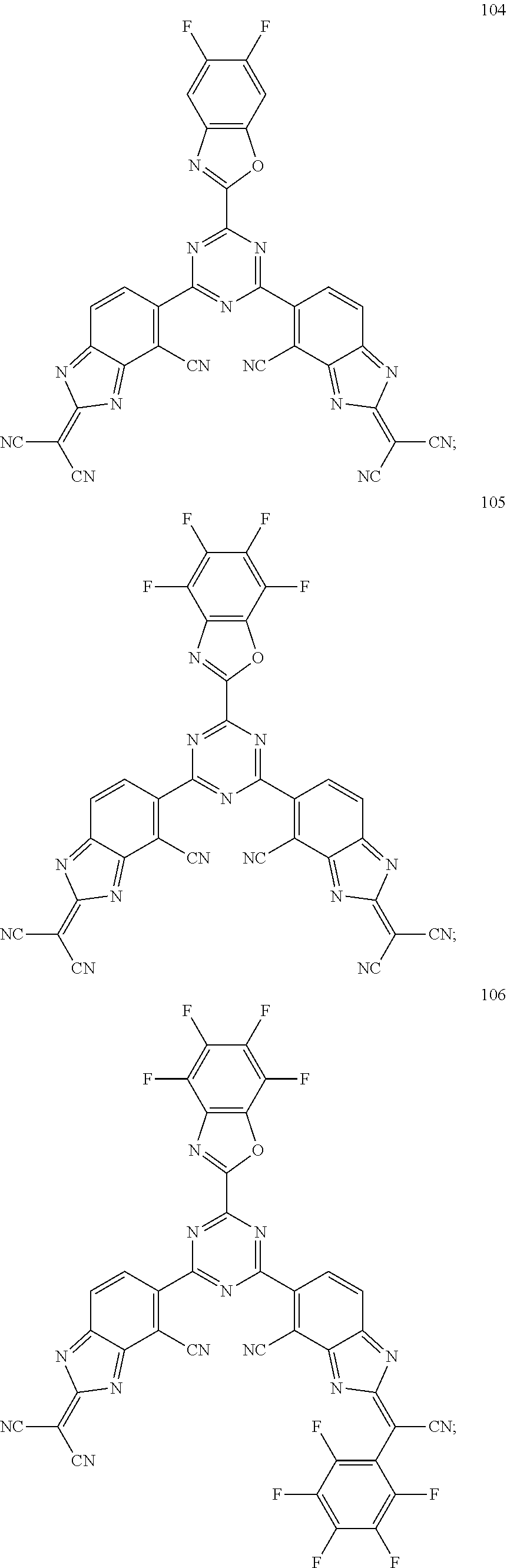
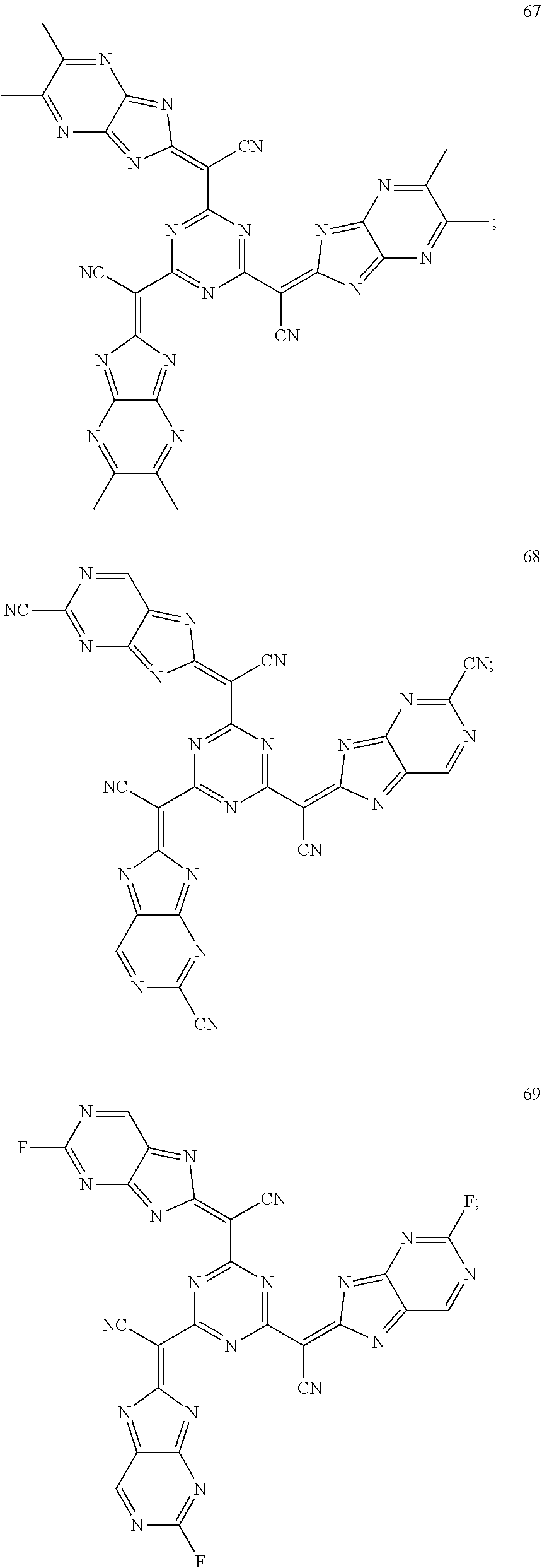
Applications Claiming Priority (2)

Application Number Priority Date Filing Date Title
KR1020190099524A KR20210020358A (en) 2019-08-14 2019-08-14 Organic compound, and organic light emitting diode and organic light emitting display device including the same
KR10-2019-0099524 2019-08-14

Publications (2)

Publication Number Publication Date
US20210050527A1 US20210050527A1 (en) 2021-02-18
US11889754B2 true US11889754B2 (en) 2024-01-30

Family

ID=74567436

Family Applications (1)

Application Number Title Priority Date Filing Date
US16/985,079 Active 2042-05-03 US11889754B2 (en) 2019-08-14 2020-08-04 Organic compound, and organic light emitting diode and organic light emitting display device including the same

Country Status (3)

Country Link
US (1) US11889754B2 (en)
KR (1) KR20210020358A (en)
CN (1) CN112390784B (en)

Families Citing this family (3)

* Cited by examiner, † Cited by third party
Publication number Priority date Publication date Assignee Title
CN113105442B (en) * 2021-02-25 2022-11-15 浙江华显光电科技有限公司 Triazine derivative, organic photoelectric element containing triazine derivative and application of organic photoelectric element
KR20230008951A (en) * 2021-07-07 2023-01-17 (주)피엔에이치테크 organic light-emitting diode with low operating voltage and High efficiency having multi-functional single hole-layer
KR20230010087A (en) * 2021-07-08 2023-01-18 (주)피엔에이치테크 An compound for multi functional hole transportation Layer and an electroluminescent device using the same

Citations (9)

* Cited by examiner, † Cited by third party
Publication number Priority date Publication date Assignee Title
US20140367645A1 (en) * 2013-06-17 2014-12-18 Samsung Display Co., Ltd. Organic light emitting diode device
CN104835921A (en) 2014-02-07 2015-08-12 罗门哈斯电子材料韩国有限公司 Organic electroluminescent device
CN106946852A (en) 2017-04-26 2017-07-14 江苏三月光电科技有限公司 It is a kind of using triazine and benzimidazole as the organic compound of core and its application on OLED
CN107056783A (en) * 2017-06-15 2017-08-18 江苏三月光电科技有限公司 A kind of compound containing azepine spiro fluorene and nitrogenous hexa-member heterocycle and its application on organic electroluminescence device
US20180166647A1 (en) * 2016-12-12 2018-06-14 Lg Display Co., Ltd. Organic compound and light emitting diode and organic light emitting diode display device using the same
CN109748909A (en) 2017-11-02 2019-05-14 江苏三月光电科技有限公司 The compound of a kind of fluorenes of xanthene containing spiral shell and nitrogenous hexa-member heterocycle, preparation method and its application in organic electroluminescence device
US20200194706A1 (en) * 2017-08-29 2020-06-18 Doosan Solus Co., Ltd. Organic electroluminescent device
US20210130336A1 (en) * 2018-04-13 2021-05-06 Idemitsu Kosan Co.,Ltd. Compound, material for organic electroluminescent elements, organic electroluminescent element, and electronic device
US20220274952A1 (en) * 2019-07-30 2022-09-01 Tosoh Corporation Cyclic azine compound, material for organic light emitting diode, electron transport material for organic light emitting diode, and organic light emitting diode

Patent Citations (11)

* Cited by examiner, † Cited by third party
Publication number Priority date Publication date Assignee Title
US20140367645A1 (en) * 2013-06-17 2014-12-18 Samsung Display Co., Ltd. Organic light emitting diode device
CN104835921A (en) 2014-02-07 2015-08-12 罗门哈斯电子材料韩国有限公司 Organic electroluminescent device
US20180166647A1 (en) * 2016-12-12 2018-06-14 Lg Display Co., Ltd. Organic compound and light emitting diode and organic light emitting diode display device using the same
CN108218858A (en) 2016-12-12 2018-06-29 乐金显示有限公司 Organic compound and light emitting diode and organic LED display device including the organic compound
US10937984B2 (en) 2016-12-12 2021-03-02 Lg Display Co., Ltd. Organic compound and light emitting diode and organic light emitting diode display device using the same
CN106946852A (en) 2017-04-26 2017-07-14 江苏三月光电科技有限公司 It is a kind of using triazine and benzimidazole as the organic compound of core and its application on OLED
CN107056783A (en) * 2017-06-15 2017-08-18 江苏三月光电科技有限公司 A kind of compound containing azepine spiro fluorene and nitrogenous hexa-member heterocycle and its application on organic electroluminescence device
US20200194706A1 (en) * 2017-08-29 2020-06-18 Doosan Solus Co., Ltd. Organic electroluminescent device
CN109748909A (en) 2017-11-02 2019-05-14 江苏三月光电科技有限公司 The compound of a kind of fluorenes of xanthene containing spiral shell and nitrogenous hexa-member heterocycle, preparation method and its application in organic electroluminescence device
US20210130336A1 (en) * 2018-04-13 2021-05-06 Idemitsu Kosan Co.,Ltd. Compound, material for organic electroluminescent elements, organic electroluminescent element, and electronic device
US20220274952A1 (en) * 2019-07-30 2022-09-01 Tosoh Corporation Cyclic azine compound, material for organic light emitting diode, electron transport material for organic light emitting diode, and organic light emitting diode

Also Published As

Publication number Publication date
CN112390784B (en) 2024-02-20
CN112390784A (en) 2021-02-23
US20210050527A1 (en) 2021-02-18
KR20210020358A (en) 2021-02-24

Similar Documents

Publication Publication Date Title
US11469378B2 (en) Electroluminescent compound and electroluminescent device including the same
US11889754B2 (en) Organic compound, and organic light emitting diode and organic light emitting display device including the same
US9257663B2 (en) Organic electroluminescent element and display device
US9450193B2 (en) Compound for organic photoelectric device and organic photoelectric device including the same
US8502201B2 (en) Light-emitting element
US11895911B2 (en) Organic light emitting device
US20130033171A1 (en) Organometallic compound and organic electroluminescence device employing the same
US11950500B2 (en) Organic light emitting diode and organic light emitting device having thereof
US11557731B2 (en) Organic light emitting diode having n-type host with narrow band gap and organic light emitting display device including the same
US11332474B2 (en) Compound and organic light-emission device
US20130001536A1 (en) Novel benzoxazolyl carbazole compound and organic light-emitting device including the same
US11384072B2 (en) Organic compound, and organic light emitting diode and organic light emitting display device including the same
US11696495B2 (en) Organic emitting compound, and organic light emitting diode and organic light emitting display device including the same
US20200194674A1 (en) Organic compound, organic light emitting diode, and organic light emitting display device including the same
US9178164B2 (en) Organic compound and organic electroluminescent device employing the same
US10693077B2 (en) Compound and organic electronic device using the same
US20210408395A1 (en) Organic compound and organic light emitting diode and organic light emitting display device including the same
US11505557B2 (en) Organic compound, and organic light emitting diode and organic light emitting display device including the same
US11374177B2 (en) Compound and organic light emitting device comprising the same
US20210305513A1 (en) Organic light emitting diode and organic light emitting device having thereof
US10693075B2 (en) Spiro compound and organic electronic device comprising the same
US20190092745A1 (en) Compound and organic electronic device using the same
US20230203075A1 (en) Organometallic compound and organic light-emitting diode including the same
US20230209989A1 (en) Organometallic compound and organic light-emitting diode including the same
US20230203074A1 (en) Organometallic compound and organic light-emitting diode including the same

Legal Events

Date Code Title Description
FEPP Fee payment procedure

Free format text: ENTITY STATUS SET TO UNDISCOUNTED (ORIGINAL EVENT CODE: BIG.); ENTITY STATUS OF PATENT OWNER: LARGE ENTITY

AS Assignment

Owner name: P&H TECH, KOREA, REPUBLIC OF

Free format text: ASSIGNMENT OF ASSIGNORS INTEREST;ASSIGNORS:HYUN, SEO-YONG;YOON, SEOK-KEUN;REEL/FRAME:053438/0253

Effective date: 20200714

Owner name: LG DISPLAY CO., LTD, KOREA, REPUBLIC OF

Free format text: ASSIGNMENT OF ASSIGNORS INTEREST;ASSIGNORS:SHIN, JI-CHEOL;YOO, SEON-KEUN;SEO, JEONG-DAE;AND OTHERS;REEL/FRAME:053438/0244

Effective date: 20200715

AS Assignment

Owner name: P&H TECH, KOREA, REPUBLIC OF

Free format text: CORRECTIVE ASSIGNMENT TO CORRECT THE ERROR ON THE COVER SHEET ATTORNEY'S SIGNATURE PREVIOUSLY RECORDED ON REEL 053438 FRAME 0253. ASSIGNOR(S) HEREBY CONFIRMS THE ASSIGNMENT;ASSIGNORS:HYUN, SEO-YONG;YOON, SEOK-KEUN;REEL/FRAME:053480/0938

Effective date: 20200714

STPP Information on status: patent application and granting procedure in general

Free format text: DOCKETED NEW CASE - READY FOR EXAMINATION

STPP Information on status: patent application and granting procedure in general

Free format text: NON FINAL ACTION MAILED

STPP Information on status: patent application and granting procedure in general

Free format text: RESPONSE TO NON-FINAL OFFICE ACTION ENTERED AND FORWARDED TO EXAMINER

STPP Information on status: patent application and granting procedure in general

Free format text: NOTICE OF ALLOWANCE MAILED -- APPLICATION RECEIVED IN OFFICE OF PUBLICATIONS

STPP Information on status: patent application and granting procedure in general

Free format text: PUBLICATIONS -- ISSUE FEE PAYMENT RECEIVED

STPP Information on status: patent application and granting procedure in general

Free format text: PUBLICATIONS -- ISSUE FEE PAYMENT VERIFIED

STCF Information on status: patent grant

Free format text: PATENTED CASE