US9082823B2 - Semiconductor device and method of manufacturing the same - Google Patents
Semiconductor device and method of manufacturing the same Download PDFInfo
- Publication number
- US9082823B2 US9082823B2 US14/185,195 US201414185195A US9082823B2 US 9082823 B2 US9082823 B2 US 9082823B2 US 201414185195 A US201414185195 A US 201414185195A US 9082823 B2 US9082823 B2 US 9082823B2
- Authority
- US
- United States
- Prior art keywords
- region
- semiconductor layer
- pair
- electrodes
- memory element
- Prior art date
- Legal status (The legal status is an assumption and is not a legal conclusion. Google has not performed a legal analysis and makes no representation as to the accuracy of the status listed.)
- Expired - Fee Related
Links
Images


Classifications
-
- H—ELECTRICITY
- H01—ELECTRIC ELEMENTS
- H01L—SEMICONDUCTOR DEVICES NOT COVERED BY CLASS H10
- H01L21/00—Processes or apparatus adapted for the manufacture or treatment of semiconductor or solid state devices or of parts thereof
- H01L21/70—Manufacture or treatment of devices consisting of a plurality of solid state components formed in or on a common substrate or of parts thereof; Manufacture of integrated circuit devices or of parts thereof
- H01L21/71—Manufacture of specific parts of devices defined in group H01L21/70
- H01L21/768—Applying interconnections to be used for carrying current between separate components within a device comprising conductors and dielectrics
- H01L21/76838—Applying interconnections to be used for carrying current between separate components within a device comprising conductors and dielectrics characterised by the formation and the after-treatment of the conductors
-
- H—ELECTRICITY
- H01—ELECTRIC ELEMENTS
- H01L—SEMICONDUCTOR DEVICES NOT COVERED BY CLASS H10
- H01L27/00—Devices consisting of a plurality of semiconductor or other solid-state components formed in or on a common substrate
- H01L27/02—Devices consisting of a plurality of semiconductor or other solid-state components formed in or on a common substrate including semiconductor components specially adapted for rectifying, oscillating, amplifying or switching and having at least one potential-jump barrier or surface barrier; including integrated passive circuit elements with at least one potential-jump barrier or surface barrier
- H01L27/04—Devices consisting of a plurality of semiconductor or other solid-state components formed in or on a common substrate including semiconductor components specially adapted for rectifying, oscillating, amplifying or switching and having at least one potential-jump barrier or surface barrier; including integrated passive circuit elements with at least one potential-jump barrier or surface barrier the substrate being a semiconductor body
- H01L27/10—Devices consisting of a plurality of semiconductor or other solid-state components formed in or on a common substrate including semiconductor components specially adapted for rectifying, oscillating, amplifying or switching and having at least one potential-jump barrier or surface barrier; including integrated passive circuit elements with at least one potential-jump barrier or surface barrier the substrate being a semiconductor body including a plurality of individual components in a repetitive configuration
- H01L27/101—Devices consisting of a plurality of semiconductor or other solid-state components formed in or on a common substrate including semiconductor components specially adapted for rectifying, oscillating, amplifying or switching and having at least one potential-jump barrier or surface barrier; including integrated passive circuit elements with at least one potential-jump barrier or surface barrier the substrate being a semiconductor body including a plurality of individual components in a repetitive configuration including resistors or capacitors only
-
- H—ELECTRICITY
- H01—ELECTRIC ELEMENTS
- H01L—SEMICONDUCTOR DEVICES NOT COVERED BY CLASS H10
- H01L21/00—Processes or apparatus adapted for the manufacture or treatment of semiconductor or solid state devices or of parts thereof
- H01L21/70—Manufacture or treatment of devices consisting of a plurality of solid state components formed in or on a common substrate or of parts thereof; Manufacture of integrated circuit devices or of parts thereof
- H01L21/71—Manufacture of specific parts of devices defined in group H01L21/70
- H01L21/768—Applying interconnections to be used for carrying current between separate components within a device comprising conductors and dielectrics
- H01L21/76838—Applying interconnections to be used for carrying current between separate components within a device comprising conductors and dielectrics characterised by the formation and the after-treatment of the conductors
- H01L21/76895—Local interconnects; Local pads, as exemplified by patent document EP0896365
-
- H—ELECTRICITY
- H01—ELECTRIC ELEMENTS
- H01L—SEMICONDUCTOR DEVICES NOT COVERED BY CLASS H10
- H01L23/00—Details of semiconductor or other solid state devices
- H01L23/52—Arrangements for conducting electric current within the device in operation from one component to another, i.e. interconnections, e.g. wires, lead frames
- H01L23/522—Arrangements for conducting electric current within the device in operation from one component to another, i.e. interconnections, e.g. wires, lead frames including external interconnections consisting of a multilayer structure of conductive and insulating layers inseparably formed on the semiconductor body
- H01L23/525—Arrangements for conducting electric current within the device in operation from one component to another, i.e. interconnections, e.g. wires, lead frames including external interconnections consisting of a multilayer structure of conductive and insulating layers inseparably formed on the semiconductor body with adaptable interconnections
- H01L23/5252—Arrangements for conducting electric current within the device in operation from one component to another, i.e. interconnections, e.g. wires, lead frames including external interconnections consisting of a multilayer structure of conductive and insulating layers inseparably formed on the semiconductor body with adaptable interconnections comprising anti-fuses, i.e. connections having their state changed from non-conductive to conductive
-
- H—ELECTRICITY
- H01—ELECTRIC ELEMENTS
- H01L—SEMICONDUCTOR DEVICES NOT COVERED BY CLASS H10
- H01L2924/00—Indexing scheme for arrangements or methods for connecting or disconnecting semiconductor or solid-state bodies as covered by H01L24/00
-
- H—ELECTRICITY
- H01—ELECTRIC ELEMENTS
- H01L—SEMICONDUCTOR DEVICES NOT COVERED BY CLASS H10
- H01L2924/00—Indexing scheme for arrangements or methods for connecting or disconnecting semiconductor or solid-state bodies as covered by H01L24/00
- H01L2924/0001—Technical content checked by a classifier
- H01L2924/0002—Not covered by any one of groups H01L24/00, H01L24/00 and H01L2224/00
Definitions
- the present disclosure relates to a semiconductor device suitable for a memory element such as an OTP (One Time Programmable) element and to a method of manufacturing the semiconductor device.
- a memory element such as an OTP (One Time Programmable) element
- the OTP element is a nonvolatile memory element capable of storing information even when an electric power source of a device is turned off.
- several structures such as a fuse-type structure and an anti-fuse-type structure have been proposed for the OTP element.
- a resistor is fused by flowing a large current to a resistive element formed of, for example, polysilicon or the like to change short-circuit state between both electrodes to open state therebetween, and thereby, an information writing operation is performed.
- a large current is flown at the time of writing as described above, a transistor having a high current ability capable of flowing a large current and a wiring having a large width capable of flowing a large current therein are necessitated. Therefore, in the fuse-type OTP element, there has been a disadvantage that the whole area including a peripheral circuit is increased.
- an alloy such as silicide
- an electrode section is melted by applying a voltage equal to or larger than a dielectric strength voltage to, for example, an MOS (Metal Oxide Semiconductor)-type capacitive element, breaking down a dielectric film, and flowing a large current.
- MOS Metal Oxide Semiconductor
- the melted metal forms a filament between electrodes, and thereby, open state between both the electrodes is changed to short-circuit state therebetween.
- an information writing operation is performed (for example, see Japanese Unexamined Patent Application Publication No. 2012-174863).
- the anti-fuse-type OTP element at the time of writing, a large current is not necessitated as much as in the fuse-type OTP element. Therefore, the anti-fuse-type OTP element is advantageous in terms of the area, and electric power consumption is allowed to be suppressed.
- a semiconductor device including: a first semiconductor layer having a first conductivity type; a pair of first electrodes arranged to be separated from each other in the first semiconductor layer; a second electrode provided on the first semiconductor layer between the pair of first electrodes with a dielectric film in between; and a pair of connection sections electrically connected to the pair of first electrodes, wherein one or both of the pair of first electrodes are divided into a first region and a second region, the first region and the second region being connected by a bridge section.
- a method of manufacturing a semiconductor device including: forming a pair of first electrodes in a first semiconductor layer having first conductive-type, one or both of the pair of first electrodes being divided into a first region and a second region; forming a dielectric film on the first semiconductor layer between the pair of first electrodes; forming a second electrode arranged on the dielectric film; forming a bride section electrically connecting the first region and the second region; and forming a pair of connection sections connected to the pair of first electrodes.
- one or both of the pair of first electrodes are divided into the first region and the second region, the bridge section electrically connecting the first region and the second region is provided, and thereby, at the time of writing, heat generated between the pair of first electrodes is confined, and heat conduction to the connection section connected to the second region is allowed to be suppressed.
- one or both of the pair of first electrodes are divided into a heat confinement region (the first region) at the time of writing and a connection region with respect to the connection section (the second region).
- FIG. 1A is a plan view illustrating a configuration of a memory element configuring a semiconductor device (memory device) according to a first embodiment of the present disclosure.
- FIG. 1B is a cross-sectional view of the memory element illustrated in FIG. 1A .
- FIG. 2A is a schematic view illustrating a configuration of the memory element illustrated in FIG. 1A before a writing operation.
- FIG. 2B is a schematic view illustrating a configuration of the memory element illustrated in FIG. 1A after the writing operation.
- FIG. 3 is a block diagram illustrating a configuration example of the memory device illustrated in FIG. 1A .
- FIG. 4 is a circuit diagram illustrating a configuration example of a memory cell illustrated in FIG. 3 .
- FIG. 5A is a cross-sectional view illustrating a method of manufacturing the memory element illustrated in FIG. 1A in order of steps.
- FIG. 5B is a cross-sectional view illustrating a step following a step of FIG. 5A .
- FIG. 5C is a cross-sectional view illustrating a step following the step of FIG. 5B .
- FIG. 5D is a cross-sectional view illustrating a step following the step of FIG. 5C .
- FIG. 5E is a cross-sectional view illustrating a step following the step of FIG. 5D .
- FIG. 5F is a cross-sectional view illustrating a step following the step of FIG. 5E .
- FIG. 6A is a plan view illustrating a configuration of a memory element as a comparative example.
- FIG. 6B is a cross-sectional view of the memory element illustrated in FIG. 6A .
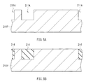
- FIG. 7A is a plan view illustrating a configuration of a memory element according to a second embodiment of the present disclosure.
- FIG. 7B is a cross-sectional view of the memory element illustrated in FIG. 7A .
- FIG. 8A is a plan view illustrating a configuration of a memory element according to a third embodiment of the present disclosure.
- FIG. 8B is a cross-sectional view of the memory element illustrated in FIG. 8A .
- FIG. 9A is a plan view illustrating a configuration of a memory element according to Modification 1 of the first embodiment.
- FIG. 9B is a cross-sectional view of the memory element illustrated in FIG. 9A .
- FIG. 10A is a plan view illustrating a configuration of a memory element according to Modification 2 of the second embodiment.
- FIG. 10B is a cross-sectional view of the memory element illustrated in FIG. 10A .
- FIG. 11A is a plan view illustrating a configuration of a memory element according to Modification 3 of the third embodiment.
- FIG. 11B is a cross-sectional view of the memory element illustrated in FIG. 11A .
- FIG. 1A illustrates a planar configuration of a semiconductor element (a memory element 21 ) configuring a semiconductor device (a memory device 1 ) according to a first embodiment of the present disclosure.
- FIG. 1B illustrates a configuration of a cross-section taken along a line I-I of the memory element 21 illustrated in FIG. 1A .
- the memory element 21 is an element in which information is stored by a writing operation. Although described in detail later, the memory element 21 is a so-called anti-fuse-type OTP element.
- the memory element 21 in this embodiment has an MOS-type transistor structure, and has a semiconductor layer 212 N and a semiconductor layer 213 N (a pair of first electrodes) that correspond to a source electrode and a drain electrode, respectively.
- the semiconductor layer 213 N (a drain electrode) is divided into a heat confinement region 213 A (a first region) and a connection region 213 B (a second region).
- the heat confinement region 213 A and the connection region 213 B are electrically connected by an electrically-conductive film 218 .
- a semiconductor layer 211 P may configure, for example, a semiconductor substrate, and may be, for example, a P-type (first conductive-type) semiconductor layer.
- the semiconductor layer 211 P may be made, for example, of a semiconductor material in which, for example, silicon (Si) or the like is doped with an impurity such as boron (B). Further, examples of the material forming the semiconductor layer 211 P are not limited thereto, and for example, an SOI (Silicon On Insulator) substrate may be used.
- the semiconductor layer 212 N and the semiconductor layer 213 N correspond to a source electrode and a drain electrode, respectively, and are arranged to be separated from each other with a predetermined space in between in the semiconductor layer 211 P.
- Each of the semiconductor layer 212 N and the semiconductor layer 213 N may be, for example, an N-type (second conductive-type) semiconductor layer (configuring a so-called N+layer).
- Each of the semiconductor layers 212 N and 213 N may be made of a semiconductor material in which, for example, Si or the like is doped with an impurity such as arsenic (As) and phosphorus (P).
- Each of the thicknesses of the semiconductor layer 212 N and the semiconductor layer 213 N may be, for example, from about 50 nm to about 200 nm both inclusive.
- the semiconductor layers 212 N and 213 N are allowed to be easily formed by a self-aligning method or a method using a mask pattern with the use of a predetermined photoresist, an oxide film, and the like in the region of the semiconductor layer 211 P.
- a distance between the semiconductor layer 212 N and the semiconductor layer 213 N may be desirably as small as possible (such as from about 50 nm to about 200 nm both inclusive), since thereby, the memory element 21 having a small element size is achievable.
- the semiconductor layer 213 N (corresponding to a drain electrode) in this embodiment is divided into the heat confinement region 213 A (the first region) and the connection region 213 B (the second region) with an element separation film 214 (an insulating film 214 A) in between.
- the heat confinement region 213 A and the connection region 213 B are electrically connected by the after-described electrically-conductive film 218 .
- the element separation film 214 integrated with the insulating film 214 A is arranged inside the semiconductor layer 211 P, and faces the top surface of the semiconductor layer 211 P.
- the element separation film 214 is arranged in the periphery of the semiconductor layer 212 N and the semiconductor layer 213 N other than the space between the semiconductor layer 212 N and the semiconductor layer 213 N.
- the element separation film 214 prevents diffusion of heat generated between the semiconductor layers 212 N and 213 N that produce heat by application of a voltage (to the semiconductor layer 213 N, in particular, to the heat confinement region 213 A).
- the element separation film 214 insulates the heat confinement region 213 A from the connection region 213 B, and thereby, protects a joint section between the connection region 213 B and an after-described contact section 215 B and the like from burnout.
- Examples of a material of the element separation film 214 may include a common insulating material such as silicon oxide (SiO 2 ) and silicon nitride (SiN x ). The thickness thereof may be, for example, from about 100 nm to about 800 nm both inclusive.
- a dielectric film 216 is provided in a region (in this example, a region between the semiconductor layers 212 N and 213 N and partial regions in the semiconductor layers 212 N and 213 N) corresponding to the space between the semiconductor layers 212 N and 213 N that is located on the semiconductor layer 211 P.
- the dielectric film 216 may be made, for example, of an insulating material (a dielectric material) similar to that of a common gate insulating film in an MOS transistor such as SiO 2 , and the thickness thereof may be, for example, from about several nm to about 20 nm both inclusive.
- An electrically-conductive film 217 corresponds to a gate electrode.
- the electrically-conductive film 217 is provided on a region where the dielectric film 216 is formed, and thereby, a laminated structure configured of the dielectric film 216 as a lower layer and the electrically-conductive film 217 as an upper layer is formed.
- the electrically-conductive film 218 is provided in a region (in this example, a region between the heat confinement region 213 A and the connection region 213 B and partial regions in the heat confinement region 213 A and the connection region 213 B) corresponding to the space between the heat confinement region 213 A and the connection region 213 B, and the heat confinement region 213 A and the connection region 213 B are electrically connected by the electrically-conductive film 218 .
- the electrically-conductive films 217 and 218 may be made, for example, of a conductive material such as polycrystal silicon and a silicide metal, and each of the thicknesses thereof may be, for example, from about 50 nm to about 500 nm both inclusive.
- the electrically-conductive film 218 may be formed of a metal material such as titanium nitride (TiN) and nickel silicide (NiSi 2 ).
- An insulating layer 219 is provided to cover the semiconductor layers 212 N and 213 N and the electrically-conductive films 217 and 218 .
- the insulating layer 219 may be made, for example, of an insulating material such as SiO 2 and SiN x , and the thickness thereof may be, for example, from about 50 nm to about 2000 nm both inclusive.
- Each of contact sections 215 A and 215 B may be made, for example, of a conductive material such as a metal such as tungsten (W) and aluminum (Al).
- the contact section 215 A is provided on the semiconductor layer 212 N and inside the element separation film 214 so that the semiconductor layer 212 N is electrically connected to a wiring layer 220 .
- the contact section 215 B is provided on the connection region 213 B of the semiconductor layer 213 N and inside the element separation film 214 so that the connection region 213 B is electrically connected to a wiring layer 221 .
- FIG. 2A illustrates a cross-sectional configuration of the memory element 21 before a writing operation
- FIG. 2B illustrates a cross-sectional configuration of the memory element 21 after the writing operation.
- the memory element 21 before the writing operation has the semiconductor layers 211 P, 212 N, and 213 N ( 213 A and 213 B); the contact sections 215 A and 215 B; the element separation film 214 ; the insulating layer 219 ; the dielectric film 216 ; and the electrically-conductive films 217 and 218 .
- an after-described filament 210 (an electrically-conductive path section) is formed in addition to the semiconductor layers 211 P, 212 N, and 213 N ( 213 A and 213 B); the contact sections 215 A and 215 B; the element separation film 214 ; the insulating layer 219 ; the dielectric film 216 ; and the electrically-conductive films 217 and 218 that are described above.
- the filament 210 is formed in the region between the semiconductor layer 212 N and the semiconductor layer 213 N through the semiconductor layer 211 P, and serves as an electrically-conductive path that electrically connects the semiconductor layers 212 N and 213 N.
- the semiconductor layers 212 N and 213 N are short-circuited (in a short-circuit state) based on a predetermined resistance value (by a resistance component) by the filament 210 .
- Such a filament 210 is formed as follows.
- the filament 210 may be formed on the following principle. That is, first, when the foregoing voltage V1 is applied between the heat confinement region 213 A of the semiconductor layer 213 N and the electrically-conducive film 217 of the memory element 21 , insulation breakdown occurs in part or all of the dielectric film 216 . Accordingly, a current suddenly flows between the electrically-conducive film 217 and the semiconductor layer 213 N. The insulation breakdown of the dielectric film 216 occurs mainly on the semiconductor layer 213 N side where the electric field intensity is relatively high.
- the insulation breakdown of the dielectric film 216 does not occur uniformly as a whole, but occurs in a local region where the insulation breakdown voltage is relatively low. Therefore, at the time of the insulation breakdown of the dielectric film 216 , the foregoing current flows locally, leading to large current density, large heat generation, and major damage in semiconductor crystal (such as silicon crystal) in a region below the dielectric film 216 in the semiconductor layer 211 P.
- a current instantaneously flows between the semiconductor layers 212 N and 213 N due to an electrical potential difference therebetween based on a leak path caused by the foregoing damage as a starting point, and junctional disruption occurs.
- Heat resulting from the current flowing at this time causes migration, which results in movement of one or both of the conductor components configuring the electrode 213 A and the contact section 215 B and the conductor component configuring the contact section 215 A into the semiconductor layer 211 P.
- the filament 210 may be formed.
- the semiconductor layers 212 N and 213 N are electrically separated (an open state).
- the semiconductor layers 212 N and 213 N are in a state of being electrically connected (a short-circuit state) by the resistance component.
- insulation breakdown occurs in part or all of the dielectric film 216 . Accordingly, the memory element 21 is allowed to serve as an anti-fuse-type OTP element.
- FIG. 3 illustrates a block configuration of the memory device 1 according to this embodiment.
- the memory device 1 is a memory device (a so-called OTP ROM (Read Only Memory)) in which, as described above, information (data) is allowed to be written only once, the written information is allowed to be read many times, and the information is not allowed to be erased.
- the memory device 1 includes a memory array 2 having a plurality of memory elements 21 (memory cells 20 ), a word line drive section 31 , and a bit line drive section/sense amplifier 32 .
- the word line drive section 31 and the bit line drive section/sense amplifier 32 correspond to drive sections (a writing operation section and a programming operation section).
- the word line drive section 31 applies a predetermined electric potential (an after-described word line electric potential) to each of a plurality of (in this example, m (m: one of integer numbers equal to or larger than 2) pieces of) word lines WL 1 to WLm that are arranged in parallel fashion in a line direction.
- a predetermined electric potential an after-described word line electric potential
- the bit line drive section/sense amplifier 32 applies a predetermined electric potential (an after-described writing operation-use voltage) to each of a plurality of (in this example, m pieces of) bit lines BL 1 to BLm that are arranged in parallel fashion in a column direction.
- the predetermined voltage V1 is applied to each of the after-described memory elements 21 in the memory cells 20 , and the after-described information writing operation is performed.
- the bit line drive section/sense amplifier 32 performs an operation of reading information from the respective memory cells 20 with the use of the foregoing m pieces of bit lines BL 1 to BLm, and has a function to perform predetermined signal amplification processing in the internal sense amplifier. It is to be noted that, on the following description, as a collective term of the bit lines BL 1 to BLm, “bit line BL” will be used as appropriate.
- the word line drive section 31 and the bit line drive section/sense amplifier 32 select one of the memory cells 20 to become a drive target (an operation target) from the plurality of memory cells 20 in the memory array 2 , and selectively performs the information writing operation or the information reading operation.
- the plurality of memory cells 20 may be arranged in a line-column state (a matrix state).
- FIG. 4 illustrates an example of a circuit configuration of the memory array 2 .
- one word line WL and one bit line BL are connected to each of the memory cells 20 .
- each of the memory cells 20 has one memory element 21 and one selective transistor 22 , and has a so-called “1T1R”-type circuit configuration.
- one word line WL is connected to a gate of one selective transistor 22 .
- One bit line BL is connected to one of the source and the drain of each of the memory elements 21
- the after-described contact section 215 B in this example, a drain electrode
- the after-described contact section 215 A in this example, a source electrode
- An electric potential of the contact section 217 (the gate electrode) is set to a predetermined electric potential (a gate electric potential Vg). That is, in each of the memory cells 20 , one memory element 21 and one selective transistor 22 are connected in series between one bit line BL and the ground GND.
- the selective transistor 22 is a transistor used to select one of the memory elements 21 to become a drive target (a writing operation target or a reading operation target), and may be configured, for example, of an MOS (Metal Oxide Semiconductor) transistor. However, the selective transistor 22 is not necessarily configured thereof, and a transistor having other structure may be used as the selective transistor 22 .
- MOS Metal Oxide Semiconductor
- the structure of the memory element 21 illustrated in FIG. 1A is allowed to be easily formed by a method similar to that of steps of forming a general MOS transistor (such as steps of forming an self-aligning source and drain with the use of a gate of an MOS transistor as a mask).
- steps of forming a general MOS transistor such as steps of forming an self-aligning source and drain with the use of a gate of an MOS transistor as a mask.
- a distance between the semiconductor layers 212 N and 213 N that are separated from each other is allowed to be decreased, and dimensions are favorably controllable.
- a concave section 211 A for arranging the element separation film 214 in the semiconductor layer 211 P may be formed, for example, by etching.
- SiO 2 may be buried into the concave section 211 A to arrange the element separation film 214 .
- an impurity is injected with the use of an ion irradiation apparatus, and thereby, the semiconductor layers 212 N and 213 N are formed in predetermined regions.
- the whole surface of the semiconductor layer 211 P in which the element separation film 214 and the semiconductor layers 212 N and 213 N are formed is coated with a dielectric film. Thereafter, portions of the dielectric film other than a predetermined region may be removed by etching or the like to form the dielectric film 216 . Subsequently, an electrically-conductive film is formed on the semiconductor layer 211 P and the dielectric film 216 by, for example, sputtering or the like, and thereafter, the electrically-conductive film may be processed by, for example, etching or the like to form the electrically-conductive films 217 and 218 .
- the whole surfaces of the semiconductor layer 211 P and the electrically-conductive films 217 and 218 are coated with the insulating layer 219 .
- through holes 219 A and 219 B are formed in predetermined positions.
- a metal material such as W may be filled into the through holes 219 A and 219 B, and thereafter, the wiring layers 220 and 221 made of, for example, Al may be formed on the insulating layer 219 . Accordingly, the memory element 21 illustrated in FIGS. 1A and 1B is completed.
- the word line drive section 31 applies the predetermined electric potential (the word line electric potential) to each of the m pieces of word lines WL 1 to WLm. Further, concurrently, the bit line drive section/sense amplifier 32 applies the predetermined electric potential (the writing operation-use voltage) to each of the m pieces of bit lines BL 1 to BLm. Thereby, one of the memory cells 20 to become a drive target (a writing operation target) is selected from the plurality of memory cells 20 in the memory array 2 , the after-described predetermined voltage V1 is applied to the memory element 21 in such a selected memory cell 20 , and thereby, the information writing operation (only once) is selectively performed.
- the predetermined electric potential the word line electric potential
- the bit line drive section/sense amplifier 32 applies the predetermined electric potential (the writing operation-use voltage) to each of the m pieces of bit lines BL 1 to BLm.
- bit line drive section/sense amplifier 32 performs the operation of reading information from one of the memory elements 21 in one of the memory cells 20 as a drive target (a reading operation target) with the use of the m pieces of bit lines BL 1 to BLm, and performs predetermined signal amplification processing in the internal sense amplifier. Thereby, the operation of reading information from one of the memory elements 21 is selectively performed.
- the predetermined electric potential (the word line electric potential) is applied to the word line WL connected to such a selected memory cell 20 , and the predetermined electric potential (the writing operation-use voltage) is applied to the bit line BL connected to such a selected memory cell 20 .
- a ground electric potential (such as 0V) is applied to each of word lines WL connected thereto, and an electric potential of each of bit lines BL connected thereto is set to a floating state or the ground electric potential (0V).
- one selective transistor 22 in the drive-target memory cell 20 is turned into on-state, the drive-target memory element 21 is selected, and thereby, the writing operation or the reading operation is performed.
- each of the memory cells 20 has one memory element 21 configured of a transistor and one selective transistor 22 .
- one word line WL is connected to the gate of one selective transistor 22 .
- One bit line BL is connected to one of the source and the drain of one selective transistor 22
- one of the source and the drain of one memory element 21 is connected to the other one of the source and the drain of one selective transistor 22 .
- the other one of the source and the drain of one memory element 21 is connected to the ground GND, and the gate is connected to a gate line GL to which a predetermined gate voltage Vg is applied.
- a voltage equal to or larger than a predetermined threshold voltage Vth is applied to the respective gates of the memory element 21 and the selective transistor 22 , and both of which are turned into on-state (the gate voltage Vg of the memory element 21 >Vth).
- a voltage not larger than respective withstand voltages of the memory element 21 and the selective transistor 22 is applied to the bit line BL, and a state in which currents respectively flow to the memory element 21 and the selective transistor 22 is set.
- FIG. 6A and FIG. 6B respectively illustrate a planar configuration and a cross-sectional configuration of a general memory element 101 .
- a gate an electrically-conductive film 1017
- a drain a semiconductor layer 1013 N
- insulation breakdown occurs in part or all of a dielectric film 1016 (part of a region on the semiconductor layer 1013 N side, for example), and thereby, a current flows between the electrically-conductive film 1017 and the semiconductor layer 1013 N.
- a filament (not illustrated) as an electrically-conductive path that electrically connects a semiconductor layer 1012 N and the semiconductor layer 1013 N is formed between the semiconductor layers 1012 N and 1013 N.
- a contact section 1015 and a wiring layer 1021 may burn out due to high heat generated at the time of applying the voltage.
- the semiconductor layer 213 N corresponding to a drain electrode is divided into the heat confinement region 213 A and the connection region 213 B, and the insulating film 214 A is arranged between the heat confinement region 213 A and the connection region 213 B.
- the electrically-conductive film 218 is provided on the insulating film 214 A, and thereby, the heat confinement region 213 A and the connection region 213 B are electrically connected.
- the semiconductor layer 213 N is divided into the heat confinement region 213 A and the connection region 213 B, and a voltage is applied between the heat confinement region 213 A and the electrically-conductive film 217 . Further, in the connection region 213 B, the contact section 215 B that connects the connection region 213 B to the wiring layer 221 is formed. Thereby, heat generated upon applying a voltage to the heat confinement region 213 A and the electrically-conductive film 217 is allowed to be confined in the heat confinement region 213 A, and burnout in the joint section between the wiring layer 221 and the contact section 215 B connecting thereto is allowed to be prevented without increasing the area of the semiconductor layer 213 N. That is, the area of the memory element 21 is allowed to be reduced.
- the memory element 21 is a gate stress-type OTP element, in which high heat generated by applying a high voltage may affect only an electrode to which the voltage is applied, in this case, only the connection section (the contact section 215 B) of the semiconductor layer 213 N. Specifically, such high heat may cause burnout only in the electrode to which the voltage is applied, in this case, only in the connection section (the contact section 215 B) of the semiconductor layer 213 N. Therefore, the area, the shape, and the like on the semiconductor layer 212 N side not affected by the burnout and the like are not particularly limited.
- FIG. 7A illustrates a planar configuration of a memory element 31 configuring a memory device 1 according to the second embodiment of the present disclosure.
- FIG. 7B illustrates a configuration of a cross-section taken along a line I-I of the memory element 31 illustrated in FIG. 7A .
- the memory element 31 is different from the foregoing first embodiment in that the heat confinement region 213 A and the connection region 213 B are electrically connected with the use of a shared contact 222 .
- the dielectric film 216 is formed in a region under the electrically-conductive film 218 as in the case of the dielectric film 216 formed in the region under the electrically-conductive film 217 , and the heat confinement region 213 A is electrically connected to the wiring layer 221 without through the connection region 213 B. Specifically, the heat confinement region 213 A is connected to the contact section 215 B through the shared contact 222 and the electrically-conductive film 218 .
- the shared contact 222 is made of a material same as the material of the foregoing contact sections 215 A and 215 B, and is formed in steps same as the steps thereof.
- the shared contact 222 may be formed to cover part of the heat confinement region 213 A, a side surface of the electrically-conductive film 218 , and part of the top surface of the electrically-conductive film 218 .
- the whole surface of the semiconductor layer 211 P in which the semiconductor layers 212 N and 213 N and the insulating film 214 A are provided is coated with a dielectric.
- an electrical conductor is formed on the dielectric film by sputtering and/or the like.
- portions of the electrically-conducive film and the dielectric film in predetermined positions such as positions on the heat confinement region 213 A and on the semiconductor layer 212 N are removed by etching, and thereby, the dielectric films 216 A and 216 B and the electrically-conducive films 217 and 218 are formed.
- the contact sections 215 A and 215 B and the shared contact 222 are formed.
- the wiring layers 220 and 221 are formed by a method similar to that of the first embodiment, and thereby, the memory device 1 illustrated in FIG. 7A and FIG. 7B is completed.
- the heat confinement region 213 A and the connection region 213 B are electrically connected with the use of the shared contact 222 . Therefore, the step of removing the dielectric film in the region where the electrically-conductive film 218 connecting the heat confinement region 213 A and the connection region 213 B is formed is omitted. That is, compared to in the first embodiment, the number of manufacturing steps is allowed to be decreased.
- the heat confinement region 213 A is directly and electrically connected to the contact section 215 B not through the connection region 213 B but thorough the shared contact 222 and the electrically-conductive film 218 . Therefore, the connection region 213 B of the semiconductor 213 N may be omitted.
- FIG. 8A illustrates a planar configuration of a memory element 41 configuring a memory device 1 according to the third embodiment of the present disclosure.
- FIG. 8B illustrates a configuration of a cross-section taken along a line I-I of the memory element 41 illustrated in FIG. 8A .
- the memory element 41 is different from the foregoing first and second embodiments in that a region having a small width is formed between the heat confinement region 213 A and the connection region 213 B of the semiconductor layer 213 N, and such a region is configured to serve as a bridge section (a bridge structure 213 C) that electrically connects the heat confinement region 213 A and the connection region 213 B.
- the bridge structure 213 C is the semiconductor layer 213 N having a small width located between the heat confinement region 213 A and the connection region 213 B. It is to be noted that, in order to suppress conduction of heat from the heat confinement region 213 A to the connection region 213 B, the thickness of the bridge structure 213 C may be preferably thin as illustrated in FIG. 8B . However, the thickness thereof may remain the same as the thickness of the semiconductor layer 213 N. By reducing the area of the semiconductor layer 213 N, heat conduction is allowed to be sufficiently decreased. Further, it may be preferable that the element separation film 214 does not exist below the bridge structure 213 C.
- the bridge structure 213 C is formed in the insulating film 214 A that separates the heat confinement region 213 A from the connection region 213 B. Therefore, the heat confinement region 213 A and the connection region 213 B are electrically connected without forming an external connection structure such as the electrically-conductive film 218 and the shared contact 222 formed in the foregoing embodiments. Thereby, the structure of the memory element 41 is allowed to be simplified without an additional step.
- Each of memory elements 51 , 61 , and 71 configuring the memory device 1 of Modifications 1 to 3 is a source-drain-type OTP element.
- the source-drain-type OTP element may operate based on the following principle. First, for example, the semiconductor layer 211 P of the memory element 51 is set to GND, a positive voltage is applied to the semiconductor layer 213 A out of the semiconductor layers 213 A and 213 B as the heat confinement region, and a negative voltage is applied to a heat confinement region 212 A. Accordingly, a voltage is applied to an interface between the semiconductor layer 213 A and the semiconductor layer 211 P.
- FIG. 9A illustrates a planar configuration of a memory element 51 according to a modification of the foregoing first embodiment.
- FIG. 9B illustrates a configuration of a cross-section taken along a line I-I of the memory element 51 illustrated in FIG. 9A .
- the semiconductor layer 212 N is divided into the heat confinement region 212 A (semiconductor layer 212 A) and a connection region 212 B that are separated with an insulating film 214 B in between.
- the heat confinement region 212 A and the connection region 212 B are electrically connected by an electrically-conductive film 218 B.
- the size and the shape of the heat confinement region 212 A are not necessarily the same as the size and the shape of the heat confinement region 213 A, and the heat confinement regions 212 A and 213 A may be independently designed. The same is similarly applied to the connection regions 212 B and 213 B.
- FIG. 10A illustrates a planar configuration of a memory element 61 according to a modification of the foregoing second embodiment.
- FIG. 10B illustrates a configuration of a cross-section taken along a line I-I of the memory element 61 illustrated in FIG. 10A .
- a structure similar to that of the semiconductor layer 213 N in the second embodiment is applied to the semiconductor layer 212 N.
- the heat confinement region 212 A and the connection region 212 B are electrically connected with the use of a shared contact 223 .
- FIG. 11A illustrates a planar configuration of a memory element 71 according to a modification of the foregoing third embodiment.
- FIG. 11B illustrates a configuration of a cross-section taken along a line I-I of the memory element 71 illustrated in FIG. 11A .
- a structure similar to that of the semiconductor layer 213 N in the third embodiment is applied to the semiconductor layer 212 N.
- the heat confinement region 212 A and the connection region 212 B are electrically connected by forming a bridge structure 212 C obtained by thinning the semiconductor layer 212 N in a groove provided in the semiconductor layer 211 .
- materials of the respective layers are not limited to the materials described in the foregoing embodiments and the like, and other materials may be used. Further, in the foregoing embodiments, the description has been given with specific examples of the configurations of the memory element, the memory cell, the memory device, and the like. However, all layers are not necessarily included, and other layers may be further included.
- the circuit configuration of the memory cell is not limited thereto. That is, on the contrary, the selective transistor 22 on the ground GND side and the memory element 21 on the bit line BL side may be connected in series.
- each of the semiconductor layers 212 N, 213 N, 222 N, and 223 N is an N-type semiconductor layer.
- the electric conductivity types (P-type and N-type) of these semiconductor layers may be opposite to the foregoing types.
- a semiconductor device may be configured of a semiconductor integrated circuit including other elements (such as a transistor, a capacitive element, and a resistance element) in addition to the foregoing memory device.
- a semiconductor device including:
- a second electrode provided on the first semiconductor layer between the pair of first electrodes with a dielectric film in between;
- one or both of the pair of first electrodes are divided into a first region and a second region, the first region and the second region being connected by a bridge section.
- a method of manufacturing a semiconductor device including:
- first semiconductor layer having first conductive-type, one or both of the pair of first electrodes being divided into a first region and a second region;
Abstract
Description
- 1. First Embodiment (an MOS transistor structure: an example in which a bridge section between a first region and a second region is formed of an electrically-conductive film)
- 1-1. Basic Configuration
- 1-2. Configuration of Memory Device
- 1-3. Manufacturing Method
- 1-4. Function and Effect
- 2. Second Embodiment (an example in which a shared contact is used for a bridge section)
- 3. Third Embodiment (an example in which a bridge section is formed in an insulating film)
- 4. Modifications (examples of source-drain-type memory elements)
- Modification 1
-
Modification 2 - Modification 3
- Other Modifications
Claims (9)
Applications Claiming Priority (2)
| Application Number | Priority Date | Filing Date | Title |
|---|---|---|---|
| JP2013037316A JP2014165444A (en) | 2013-02-27 | 2013-02-27 | Semiconductor device and manufacturing method of the same |
| JP2013-037316 | 2013-02-27 |
Publications (2)
| Publication Number | Publication Date |
|---|---|
| US20140239441A1 US20140239441A1 (en) | 2014-08-28 |
| US9082823B2 true US9082823B2 (en) | 2015-07-14 |
Family
ID=51369633
Family Applications (1)
| Application Number | Title | Priority Date | Filing Date |
|---|---|---|---|
| US14/185,195 Expired - Fee Related US9082823B2 (en) | 2013-02-27 | 2014-02-20 | Semiconductor device and method of manufacturing the same |
Country Status (3)
| Country | Link |
|---|---|
| US (1) | US9082823B2 (en) |
| JP (1) | JP2014165444A (en) |
| CN (1) | CN104009038A (en) |
Citations (2)
| Publication number | Priority date | Publication date | Assignee | Title |
|---|---|---|---|---|
| JP2012174863A (en) | 2011-02-21 | 2012-09-10 | Sony Corp | Semiconductor device and operation method of the same |
| US20130058150A1 (en) * | 2011-09-05 | 2013-03-07 | Renesas Electronics Corporation | Otp memory |
-
2013
- 2013-02-27 JP JP2013037316A patent/JP2014165444A/en active Pending
-
2014
- 2014-02-18 CN CN201410054310.1A patent/CN104009038A/en active Pending
- 2014-02-20 US US14/185,195 patent/US9082823B2/en not_active Expired - Fee Related
Patent Citations (2)
| Publication number | Priority date | Publication date | Assignee | Title |
|---|---|---|---|---|
| JP2012174863A (en) | 2011-02-21 | 2012-09-10 | Sony Corp | Semiconductor device and operation method of the same |
| US20130058150A1 (en) * | 2011-09-05 | 2013-03-07 | Renesas Electronics Corporation | Otp memory |
Also Published As
| Publication number | Publication date |
|---|---|
| US20140239441A1 (en) | 2014-08-28 |
| CN104009038A (en) | 2014-08-27 |
| JP2014165444A (en) | 2014-09-08 |
Similar Documents
| Publication | Publication Date | Title |
|---|---|---|
| US8797782B2 (en) | Semiconductor device and operation method thereof | |
| JP4981661B2 (en) | Split channel antifuse array structure | |
| US9502424B2 (en) | Integrated circuit device featuring an antifuse and method of making same | |
| TWI518849B (en) | Electronic device including a nonvolatile memory structure having an antifuse component and a process of forming the same | |
| JP5893662B2 (en) | Nonvolatile memory cell structure and method for programming and reading the same | |
| US9336895B2 (en) | Memory device, semiconductor unit and method of operating the same, and electronic apparatus | |
| JP2009117461A (en) | Antifuse element and method of setting antifuse element | |
| WO2006121828A2 (en) | One time programmable memory cell | |
| TWI747528B (en) | Small area low voltage anti-fuse element and array | |
| US8611129B2 (en) | Semiconductor device and operation method thereof | |
| US9478307B2 (en) | Memory device, writing method, and reading method | |
| TW201803079A (en) | Semiconductor device | |
| US9842802B2 (en) | Integrated circuit device featuring an antifuse and method of making same | |
| US20150206595A1 (en) | Antifuse array architecture | |
| US20140268984A1 (en) | Semiconductor device and electronic apparatus | |
| JP2006059919A (en) | Mos electric fuse, its programming method, and semiconductor device using it | |
| JP5596467B2 (en) | Method for writing to semiconductor device and memory device | |
| US6949423B1 (en) | MOSFET-fused nonvolatile read-only memory cell (MOFROM) | |
| CN107492553B (en) | Three-transistor OTP memory cell | |
| US9082823B2 (en) | Semiconductor device and method of manufacturing the same | |
| CN106133841B (en) | One-time programmable memory, electronic system, method for operating one-time programmable memory and method for programming one-time programmable memory | |
| CN109671710B (en) | OTP cell with improved programmability | |
| US10355003B2 (en) | Anti-fuses memory cell and memory apparatus | |
| US9941017B1 (en) | Antifuse one-time programmable semiconductor memory |
Legal Events
| Date | Code | Title | Description |
|---|---|---|---|
| AS | Assignment |
Owner name: SONY CORPORATION, JAPAN Free format text: ASSIGNMENT OF ASSIGNORS INTEREST;ASSIGNORS:KOBAYASHI, SHOJI;YANAGISAWA, YUKI;REEL/FRAME:032301/0597 Effective date: 20140122 |
|
| STCF | Information on status: patent grant |
Free format text: PATENTED CASE |
|
| FEPP | Fee payment procedure |
Free format text: PAYOR NUMBER ASSIGNED (ORIGINAL EVENT CODE: ASPN); ENTITY STATUS OF PATENT OWNER: LARGE ENTITY |
|
| MAFP | Maintenance fee payment |
Free format text: PAYMENT OF MAINTENANCE FEE, 4TH YEAR, LARGE ENTITY (ORIGINAL EVENT CODE: M1551); ENTITY STATUS OF PATENT OWNER: LARGE ENTITY Year of fee payment: 4 |
|
| FEPP | Fee payment procedure |
Free format text: MAINTENANCE FEE REMINDER MAILED (ORIGINAL EVENT CODE: REM.); ENTITY STATUS OF PATENT OWNER: LARGE ENTITY |
|
| LAPS | Lapse for failure to pay maintenance fees |
Free format text: PATENT EXPIRED FOR FAILURE TO PAY MAINTENANCE FEES (ORIGINAL EVENT CODE: EXP.); ENTITY STATUS OF PATENT OWNER: LARGE ENTITY |
|
| STCH | Information on status: patent discontinuation |
Free format text: PATENT EXPIRED DUE TO NONPAYMENT OF MAINTENANCE FEES UNDER 37 CFR 1.362 |
|
| FP | Lapsed due to failure to pay maintenance fee |
Effective date: 20230714 |