US9081248B2 - Reflector and display device having the same - Google Patents
Reflector and display device having the same Download PDFInfo
- Publication number
- US9081248B2 US9081248B2 US13/421,438 US201213421438A US9081248B2 US 9081248 B2 US9081248 B2 US 9081248B2 US 201213421438 A US201213421438 A US 201213421438A US 9081248 B2 US9081248 B2 US 9081248B2
- Authority
- US
- United States
- Prior art keywords
- reflective layer
- light
- refractive index
- display device
- reflector
- Prior art date
- Legal status (The legal status is an assumption and is not a legal conclusion. Google has not performed a legal analysis and makes no representation as to the accuracy of the status listed.)
- Active, expires
Links
Images


Classifications
-
- G—PHYSICS
- G02—OPTICS
- G02B—OPTICAL ELEMENTS, SYSTEMS OR APPARATUS
- G02B5/00—Optical elements other than lenses
- G02B5/08—Mirrors
- G02B5/0816—Multilayer mirrors, i.e. having two or more reflecting layers
-
- G—PHYSICS
- G02—OPTICS
- G02F—OPTICAL DEVICES OR ARRANGEMENTS FOR THE CONTROL OF LIGHT BY MODIFICATION OF THE OPTICAL PROPERTIES OF THE MEDIA OF THE ELEMENTS INVOLVED THEREIN; NON-LINEAR OPTICS; FREQUENCY-CHANGING OF LIGHT; OPTICAL LOGIC ELEMENTS; OPTICAL ANALOGUE/DIGITAL CONVERTERS
- G02F1/00—Devices or arrangements for the control of the intensity, colour, phase, polarisation or direction of light arriving from an independent light source, e.g. switching, gating or modulating; Non-linear optics
- G02F1/01—Devices or arrangements for the control of the intensity, colour, phase, polarisation or direction of light arriving from an independent light source, e.g. switching, gating or modulating; Non-linear optics for the control of the intensity, phase, polarisation or colour
- G02F1/165—Devices or arrangements for the control of the intensity, colour, phase, polarisation or direction of light arriving from an independent light source, e.g. switching, gating or modulating; Non-linear optics for the control of the intensity, phase, polarisation or colour based on translational movement of particles in a fluid under the influence of an applied field
- G02F1/166—Devices or arrangements for the control of the intensity, colour, phase, polarisation or direction of light arriving from an independent light source, e.g. switching, gating or modulating; Non-linear optics for the control of the intensity, phase, polarisation or colour based on translational movement of particles in a fluid under the influence of an applied field characterised by the electro-optical or magneto-optical effect
- G02F1/167—Devices or arrangements for the control of the intensity, colour, phase, polarisation or direction of light arriving from an independent light source, e.g. switching, gating or modulating; Non-linear optics for the control of the intensity, phase, polarisation or colour based on translational movement of particles in a fluid under the influence of an applied field characterised by the electro-optical or magneto-optical effect by electrophoresis
-
- G—PHYSICS
- G02—OPTICS
- G02B—OPTICAL ELEMENTS, SYSTEMS OR APPARATUS
- G02B5/00—Optical elements other than lenses
- G02B5/20—Filters
- G02B5/201—Filters in the form of arrays
-
- G—PHYSICS
- G02—OPTICS
- G02B—OPTICAL ELEMENTS, SYSTEMS OR APPARATUS
- G02B5/00—Optical elements other than lenses
- G02B5/20—Filters
- G02B5/28—Interference filters
- G02B5/285—Interference filters comprising deposited thin solid films
-
- G—PHYSICS
- G02—OPTICS
- G02F—OPTICAL DEVICES OR ARRANGEMENTS FOR THE CONTROL OF LIGHT BY MODIFICATION OF THE OPTICAL PROPERTIES OF THE MEDIA OF THE ELEMENTS INVOLVED THEREIN; NON-LINEAR OPTICS; FREQUENCY-CHANGING OF LIGHT; OPTICAL LOGIC ELEMENTS; OPTICAL ANALOGUE/DIGITAL CONVERTERS
- G02F1/00—Devices or arrangements for the control of the intensity, colour, phase, polarisation or direction of light arriving from an independent light source, e.g. switching, gating or modulating; Non-linear optics
- G02F1/01—Devices or arrangements for the control of the intensity, colour, phase, polarisation or direction of light arriving from an independent light source, e.g. switching, gating or modulating; Non-linear optics for the control of the intensity, phase, polarisation or colour
- G02F1/13—Devices or arrangements for the control of the intensity, colour, phase, polarisation or direction of light arriving from an independent light source, e.g. switching, gating or modulating; Non-linear optics for the control of the intensity, phase, polarisation or colour based on liquid crystals, e.g. single liquid crystal display cells
- G02F1/133—Constructional arrangements; Operation of liquid crystal cells; Circuit arrangements
- G02F1/1333—Constructional arrangements; Manufacturing methods
- G02F1/1335—Structural association of cells with optical devices, e.g. polarisers or reflectors
- G02F1/133509—Filters, e.g. light shielding masks
- G02F1/133514—Colour filters
-
- G—PHYSICS
- G02—OPTICS
- G02F—OPTICAL DEVICES OR ARRANGEMENTS FOR THE CONTROL OF LIGHT BY MODIFICATION OF THE OPTICAL PROPERTIES OF THE MEDIA OF THE ELEMENTS INVOLVED THEREIN; NON-LINEAR OPTICS; FREQUENCY-CHANGING OF LIGHT; OPTICAL LOGIC ELEMENTS; OPTICAL ANALOGUE/DIGITAL CONVERTERS
- G02F1/00—Devices or arrangements for the control of the intensity, colour, phase, polarisation or direction of light arriving from an independent light source, e.g. switching, gating or modulating; Non-linear optics
- G02F1/01—Devices or arrangements for the control of the intensity, colour, phase, polarisation or direction of light arriving from an independent light source, e.g. switching, gating or modulating; Non-linear optics for the control of the intensity, phase, polarisation or colour
- G02F1/165—Devices or arrangements for the control of the intensity, colour, phase, polarisation or direction of light arriving from an independent light source, e.g. switching, gating or modulating; Non-linear optics for the control of the intensity, phase, polarisation or colour based on translational movement of particles in a fluid under the influence of an applied field
- G02F1/1675—Constructional details
- G02F1/1677—Structural association of cells with optical devices, e.g. reflectors or illuminating devices
-
- G—PHYSICS
- G02—OPTICS
- G02F—OPTICAL DEVICES OR ARRANGEMENTS FOR THE CONTROL OF LIGHT BY MODIFICATION OF THE OPTICAL PROPERTIES OF THE MEDIA OF THE ELEMENTS INVOLVED THEREIN; NON-LINEAR OPTICS; FREQUENCY-CHANGING OF LIGHT; OPTICAL LOGIC ELEMENTS; OPTICAL ANALOGUE/DIGITAL CONVERTERS
- G02F1/00—Devices or arrangements for the control of the intensity, colour, phase, polarisation or direction of light arriving from an independent light source, e.g. switching, gating or modulating; Non-linear optics
- G02F1/01—Devices or arrangements for the control of the intensity, colour, phase, polarisation or direction of light arriving from an independent light source, e.g. switching, gating or modulating; Non-linear optics for the control of the intensity, phase, polarisation or colour
- G02F1/165—Devices or arrangements for the control of the intensity, colour, phase, polarisation or direction of light arriving from an independent light source, e.g. switching, gating or modulating; Non-linear optics for the control of the intensity, phase, polarisation or colour based on translational movement of particles in a fluid under the influence of an applied field
- G02F1/1675—Constructional details
- G02F1/1679—Gaskets; Spacers; Sealing of cells; Filling or closing of cells
- G02F1/1681—Gaskets; Spacers; Sealing of cells; Filling or closing of cells having two or more microcells partitioned by walls, e.g. of microcup type
-
- G—PHYSICS
- G02—OPTICS
- G02F—OPTICAL DEVICES OR ARRANGEMENTS FOR THE CONTROL OF LIGHT BY MODIFICATION OF THE OPTICAL PROPERTIES OF THE MEDIA OF THE ELEMENTS INVOLVED THEREIN; NON-LINEAR OPTICS; FREQUENCY-CHANGING OF LIGHT; OPTICAL LOGIC ELEMENTS; OPTICAL ANALOGUE/DIGITAL CONVERTERS
- G02F1/00—Devices or arrangements for the control of the intensity, colour, phase, polarisation or direction of light arriving from an independent light source, e.g. switching, gating or modulating; Non-linear optics
- G02F1/01—Devices or arrangements for the control of the intensity, colour, phase, polarisation or direction of light arriving from an independent light source, e.g. switching, gating or modulating; Non-linear optics for the control of the intensity, phase, polarisation or colour
- G02F1/13—Devices or arrangements for the control of the intensity, colour, phase, polarisation or direction of light arriving from an independent light source, e.g. switching, gating or modulating; Non-linear optics for the control of the intensity, phase, polarisation or colour based on liquid crystals, e.g. single liquid crystal display cells
- G02F1/133—Constructional arrangements; Operation of liquid crystal cells; Circuit arrangements
- G02F1/1333—Constructional arrangements; Manufacturing methods
- G02F1/1335—Structural association of cells with optical devices, e.g. polarisers or reflectors
- G02F1/133509—Filters, e.g. light shielding masks
- G02F1/133514—Colour filters
- G02F1/133521—Interference filters
-
- G—PHYSICS
- G02—OPTICS
- G02F—OPTICAL DEVICES OR ARRANGEMENTS FOR THE CONTROL OF LIGHT BY MODIFICATION OF THE OPTICAL PROPERTIES OF THE MEDIA OF THE ELEMENTS INVOLVED THEREIN; NON-LINEAR OPTICS; FREQUENCY-CHANGING OF LIGHT; OPTICAL LOGIC ELEMENTS; OPTICAL ANALOGUE/DIGITAL CONVERTERS
- G02F1/00—Devices or arrangements for the control of the intensity, colour, phase, polarisation or direction of light arriving from an independent light source, e.g. switching, gating or modulating; Non-linear optics
- G02F1/01—Devices or arrangements for the control of the intensity, colour, phase, polarisation or direction of light arriving from an independent light source, e.g. switching, gating or modulating; Non-linear optics for the control of the intensity, phase, polarisation or colour
- G02F1/165—Devices or arrangements for the control of the intensity, colour, phase, polarisation or direction of light arriving from an independent light source, e.g. switching, gating or modulating; Non-linear optics for the control of the intensity, phase, polarisation or colour based on translational movement of particles in a fluid under the influence of an applied field
- G02F1/1675—Constructional details
- G02F2001/1678—Constructional details characterised by the composition or particle type
-
- G—PHYSICS
- G02—OPTICS
- G02F—OPTICAL DEVICES OR ARRANGEMENTS FOR THE CONTROL OF LIGHT BY MODIFICATION OF THE OPTICAL PROPERTIES OF THE MEDIA OF THE ELEMENTS INVOLVED THEREIN; NON-LINEAR OPTICS; FREQUENCY-CHANGING OF LIGHT; OPTICAL LOGIC ELEMENTS; OPTICAL ANALOGUE/DIGITAL CONVERTERS
- G02F2201/00—Constructional arrangements not provided for in groups G02F1/00 - G02F7/00
- G02F2201/34—Constructional arrangements not provided for in groups G02F1/00 - G02F7/00 reflector
-
- G—PHYSICS
- G02—OPTICS
- G02F—OPTICAL DEVICES OR ARRANGEMENTS FOR THE CONTROL OF LIGHT BY MODIFICATION OF THE OPTICAL PROPERTIES OF THE MEDIA OF THE ELEMENTS INVOLVED THEREIN; NON-LINEAR OPTICS; FREQUENCY-CHANGING OF LIGHT; OPTICAL LOGIC ELEMENTS; OPTICAL ANALOGUE/DIGITAL CONVERTERS
- G02F2203/00—Function characteristic
- G02F2203/02—Function characteristic reflective
-
- G—PHYSICS
- G02—OPTICS
- G02F—OPTICAL DEVICES OR ARRANGEMENTS FOR THE CONTROL OF LIGHT BY MODIFICATION OF THE OPTICAL PROPERTIES OF THE MEDIA OF THE ELEMENTS INVOLVED THEREIN; NON-LINEAR OPTICS; FREQUENCY-CHANGING OF LIGHT; OPTICAL LOGIC ELEMENTS; OPTICAL ANALOGUE/DIGITAL CONVERTERS
- G02F2203/00—Function characteristic
- G02F2203/05—Function characteristic wavelength dependent
- G02F2203/055—Function characteristic wavelength dependent wavelength filtering
Definitions
- the present invention relates to a display device, and more particularly, to a high efficiency reflector which reflects multiple color light, and to a display device which can increase display quality by applying the high efficiency reflector thereto.
- Electrophoretic display devices denote devices that display an image with electrophoresis in which colored charged particles move by an electric field given from the outside.
- electrophoresis denotes an electrophoretic motion where with charged particles being dispersed into a solvent, the charged particles moves inside the solvent by Coulomb force when applying an electric field.
- Electrophoretic display devices using electrophoresis have bistability, and thus can maintain a displayed image for a long time even when an applied voltage is removed. That is, since electrophoretic display devices maintain a constant screen for a long time even when a voltage is not continuously applied thereto, the electrophoretic display devices are display devices suitable for an e-book field that does not require the quick change of a screen.
- electrophoretic display devices are not dependent on a viewing angle unlike Liquid Crystal Display (LCD) devices, and moreover, provide an image comfortable for eyes by the degree similar to papers because reflecting external light to display an image. Furthermore, electrophoretic display devices have flexibility, low power consumption, and eco like. Accordingly, the demand of electrophoretic display devices is increasing.
- LCD Liquid Crystal Display
- FIG. 1 is a sectional view illustrating a related art electrophoretic display device.
- the related art electrophoretic display device includes a lower substrate 10 and an upper substrate 20 that are facing-coupled to each other, and an electrophoretic film 30 disposed between the lower substrate 10 and the upper substrate 20 .
- the lower substrate 10 includes a plurality of pixel electrodes (not shown), and a plurality of thin film transistors (TFT, not shown) for respectively applying a voltage to the pixel electrodes.
- TFT thin film transistor
- a common electrode 22 is formed at the upper substrate 20 .
- the electrophoretic film 30 includes a plurality of microcapsules 32 that are formed of charged particles and a solvent, and an adhesive layer 34 that protects the microcapsules 32 and is adhesive to the lower substrate 10 .
- each of the microcapsules 32 includes positive charged particles, negative charged particles, and a solvent that surrounds each of the positive and negative charged particles.
- the charged particles included in the microcapsules 32 move toward the upper substrate 20 or the lower substrate 10 by electrophoresis, thereby realizing an image.
- the lower substrate 10 that is formed through a separate process, the upper substrate 20 that is formed by a separate process different from the formation process of the lower substrate 10 , and the electrophoretic film 30 that is adhered to the upper substrate 20 by a lamination process are manufactured separately, and then by coupling the two substrates 10 and 20 , the related art electrophoretic display device is completed.
- the electrophoretic film 30 is managed and conveyed, with the electrophoretic film 30 being adhered to the upper substrate 20 .
- the passivation layer adhered to the adhesive layer 34 is removed from the upper substrate 20 with the electrophoretic film 30 adhered thereto so as to expose the adhesive layer 34 .
- the electrophoretic display device is completed.
- the related art electrophoretic display device displays an image by using the reflection of external light, but has a low contrast ratio and a low color reproduction ratio because the light reflection efficiencies of the microcapsules 32 are low.
- a structure was proposed where a metal reflector is formed on a lower substrate and thus increases a light reflection rate, but in the structure, since a plurality of parasitic capacitors are formed between the reflector and the pixels of the lower substrate, the parasitic capacitors exert a bad influence on the driving of the pixels.
- the related art In applying the metal reflector of the related art, in order not to affect the driving of an active matrix of pixels, the related art requires a patterning process and a process that deposits a metal material over the metal reflector.
- the metal reflector of the related art reflects only 40% of incident light, and thus has limitations in increasing luminance, a contrast ratio, and a color reproduction ratio.
- the present invention is directed to provide a reflector and a display device having the same that substantially obviate one or more problems due to limitations and disadvantages of the related art.
- An aspect of the present invention is directed to provide a display device which has high luminance, a high contrast ratio, and a high color reproduction ratio.
- Another aspect of the present invention is directed to provide a high efficiency reflector which can increase the light efficiency of reflective display devices and self-emitting display devices.
- Another aspect of the present invention is directed to provide an electrophoretic display device which can realize a high-quality image in various colors.
- a reflector including: a first reflective layer pair reflecting red light; a second reflective layer pair reflecting green light; and a third reflective layer pair reflecting blue light, wherein the first to third reflective layer pairs are formed as a plurality of inorganic layers.
- a reflector including: a plurality of reflective layer pairs including a first reflective layer having a first refractive index, and a second reflective layer having a refractive index lower than the first refractive index, wherein the reflective layer pairs are formed to have different thicknesses, and selectively reflect incident light according to wavelengths.
- FIG. 1 is a view illustrating a structure of a related art electrophorectic display device
- FIG. 2 is a view illustrating a display device according to an embodiment of the present invention.
- FIG. 3 is a view illustrating a reflector of the display device according to an embodiment of the present invention.
- FIG. 4 is a view showing the thicknesses of a low refractive index reflection layer by reflection wavelength
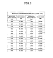
- FIG. 5 is a view showing the thicknesses of a high refractive index reflection layer by reflection wavelength
- FIG. 6 is a view showing light reflection rates with respect to the number of low refractive index reflection layer-high refractive index reflection layer pairs;
- FIGS. 7 to 9 are views illustrating an image realization method of a display device according to an embodiment of the present invention.
- FIG. 10 is a view illustrating a display device according to another embodiment of the present invention.
- a display device may include a reflective display device, a self-emitting display device, and a semi-transmissive display device.
- a reflective display device specifically, an electrophoretic display device will be described as an example of the present invention.
- an electrophoretic display device including a mono type and a color filter, and an electrophoretic display device where charged particles in a display solvent (e-ink) are colored in at least one of black, white, red, blue, green, yellow, cyan, and magenta.
- a display solvent e-ink
- FIG. 2 is a view illustrating a display device according to an embodiment of the present invention.
- the display device includes an upper substrate 170 , a lower substrate 110 , and an electrophoretic layer with a display solvent internalized therein.
- the upper substrate 170 includes: a plurality of color filters 172 that respectively convert the input light and output light of a plurality of pixels into multiple color light; a light blocking layer 174 (for example, a black matrix) that defines the pixels and prevents color mixture between the pixels; an overcoat layer 176 that planarizes the upper substrate 170 ; and a common electrode 180 .
- a light blocking layer 174 for example, a black matrix
- the color filters 172 may be configured with a plurality of red color filters, green color filters, and blue color filters.
- the upper substrate 170 is required to be transparent for displaying an image, and thus uses a transparent glass substrate or a flexible and transparent plastic substrate as a base substrate.
- the common electrode 180 of the upper substrate 170 is formed in correspondence with a plurality of pixel electrodes 114 formed at the lower substrate 110 , and supplies a common voltage Vcom to the pixels.
- the common electrode 180 transmits light incident from the outside and light that is reflected by the below-described reflector 130 .
- the common electrode 180 is formed of a conductive transparent material such as indium tin oxide (ITO) or indium zinc oxide (IZO).
- the common electrode 180 is illustrated as being formed in a plate shape to correspond to all the pixels, but this is to illustrate one embodiment of the present invention. As another embodiment of the present invention, the common electrode 180 may be patterned and formed to correspond to all or some of the pixels.
- the lower substrate 110 includes a plurality of thin film transistors (TFTs) 112 that respectively drive the pixels; a plurality of pixel electrodes 114 that receive a plurality of pixel voltages which correspond to input image data and are supplied to the pixels, respectively; and a reflector 130 that reflects light incident on the pixels.
- TFTs thin film transistors
- the electrophoretic layer is formed on the reflector 130 .
- the lower substrate 110 may apply a transparent glass substrate, a plastic substrate having flexibility, or a metal substrate having flexibility thereto as the base substrate. However, the lower substrate 110 is disposed on the reverse of a screen displaying an image, thus requiring no transparency.
- a plurality of intersected gate lines and data lines are formed at the lower substrate 110 , and the TFT 112 is formed in each of a plurality of regions where the gate lines and the data lines are intersected perpendicularly.
- the gate lines and the data lines may be formed in a single layer that is formed of silver (Ag), aluminum (Al), or an alloy thereof, which has low resistivity.
- the gate lines and the data lines may be formed in a multilayer that includes the single layer and a layer which is formed of chromium (Cr), titanium (Ti), or tantalum (Ta), which has excellent electric characteristic.
- a gate electrode of each of the TFTs 112 is connected to a corresponding gate line, a source electrode of the TFT 112 is connected to a corresponding data line, and a drain electrode of the TFT 112 is connected to a corresponding pixel electrode 114 .
- a data voltage applied to the data line is supplied to the pixel electrode 114 through switching in the TFT 112 .
- the pixel electrodes 114 are formed in respective correspondence with a plurality of pixel regions that are defined by a plurality of partition walls 140 .
- Each of the pixel electrodes 114 receives a data voltage which is inputted to a corresponding pixel by switching of a corresponding TFT 112 .
- each pixel electrode 114 may be formed in a central portion of a corresponding pixel region so as to smoothly realize an image by the electrophoretic driving of charged particles 160 .
- the pixel electrode 114 is a conductive metal layer, electrically connected to the drain electrode of the TFT 112 through a contact hole, and formed of copper (Cu), Al, or ITO. Also, the pixel electrode 114 may be formed by depositing nickel (Ni) and/or gold (Au) on Cu, Al, or ITO.
- An electric field is generated in each pixel by the common voltage Vcom applied to a pixel through the common electrode 180 and a data voltage applied to the pixel through a corresponding pixel electrode 114 , and the charged particles 160 move upward and downward in a solvent 150 by the electric field generated in each pixel, thereby realizing an image.
- the electrophoretic layer includes a display solvent that is filled into each pixel region (filling cell) that is defined by corresponding partition walls 140 .
- each of the partition walls 140 is formed to surround a corresponding pixel, and the display solvent is filled and internalized into each pixel region that is defined by corresponding partition walls 140 .
- the display solvent includes the charged particles 160 that are colored in a certain color (for example, black), and the solvent 150 that acts as a medium enabling the moving of the charged particles 160 .
- the solvent 150 may include a binder for increasing the bistability of the charged particles 160 .
- the partition walls 140 are formed on the lower substrate 110 where the below-described reflector 130 is formed, and define a plurality of regions (filling cells) into which the display solvent is filled.
- the partition walls 140 are formed to have a certain height and a certain width.
- the partition walls 140 may be formed to have a height of 10 um to 100 um and a width of 5 um to 30 um.
- the partition walls 140 may be formed by a photolithography process, a mold printing process, an imprinting process, or an embossing process.
- the partition walls 140 may be formed of a polymer, an organic material such as an epoxy acrylic-based resin, or an organic material that is capable of being coated in the shape of an organic Self-Assembled Monolayer (SAM) layer.
- SAM organic Self-Assembled Monolayer
- the charged particles 160 may be electrically charged to a positive (+) polarity or a negative ( ⁇ ) polarity, and colored in at least one of black, white, red, blue, green, yellow, cyan, and magenta.
- the charged particles 160 are exemplarily illustrated as being colored in black.
- the solvent 155 may use one of halogenated solvents, saturated hydrocarbons, silicone oils, low molecular weight halogen-containing polymers, epoxides, vinyl ethers, vinyl ester, aromatic hydrocarbon, toluene, naphthalene, paraffinic liquids, and poly chlorotrifluoroethylene polymers, or use materials, which are selected from among the materials, in combination.
- the display solvent may be filled into a corresponding pixel region by a die coating process, a casting process, a bar coating process, a slit coating process, a dispense process, a squeezing process, a screen printing process, an inkjet printing process, or a photolithography process.
- FIG. 3 is a view illustrating a reflector of the display device according to an embodiment of the present invention.
- the reflector 130 includes a plurality of reflective layers 131 to 136 .
- the reflective layer 131 of a high refractive index (n 1 ) and the reflective layer 132 of a low refractive index (n 2 ) form one pair A
- the reflective layer 133 of a high refractive index (n 1 ) and the reflective layer 134 of a low refractive index (n 2 ) form one pair B
- the reflective layer 135 of a high refractive index (n 1 ) and the reflective layer 136 of a low refractive index (n 2 ) form one pair C.
- the reflector 130 has a structure where the reflective layer pairs A to C are sequentially stacked iteratively.
- the high refractive index reflective layers 131 , 133 and 135 (high refractive index inorganic layer) and the low refractive index reflective layers 132 , 134 and 135 (low refractive index inorganic layer) are formed as insulation layers of nonconductive materials.
- the high refractive index reflective layers 131 , 133 and 135 may have a refractive index of 1.9 to 2.8. and may be formed of any one inorganic material of TiO 2 , SiNx, ZnO, and Al 2 O 3 . Alternatively, the high refractive index reflective layers 131 , 133 and 135 may also be formed by selectively combining at least two materials of TiO 2 , SiNx, ZnO, and Al 2 O 3 .
- the low refractive index reflective layers 132 , 134 and 136 may have a refractive index of 1.3 to 1.7. and may be formed by using SiO 2 as an inorganic material. Alternatively, the low refractive index reflective layers 132 , 134 and 136 may also be formed of an inorganic material including SiO 2 .
- the reflective layers 131 to 136 may be formed by a sputtering process or a Chemical Vapor Deposition (CVD) process.
- the reflective layers 131 to 136 may be formed by a spin coating process or a spray process.
- the reflector 130 is formed of a plurality of inorganic insulators, and thus does not affect the driving of the pixel electrode 114 and common electrode 180 .
- the reflective layers are stacked in order from the high refractive index (n 1 ) reflective layers 131 , 133 and 135 to the low refractive index (n 2 ) reflective layers 132 , 134 and 136 , but the order in which the high refractive index (n 1 ) reflective layers and the low refractive index (n 2 ) reflective layers are stacked is not limited thereto.
- the reflector 130 may be formed such that the number of high refractive index reflective layer-low refractive index reflective layer pairs (the number of reflective layer pairs) is a minimum of two to a maximum of ten.
- a reflection rate (R DBR ) of light incident on a reflector is determined with a refractive index ( n h ) of the high refractive index reflective layer, a refractive index ( n l ) of the low refractive index reflective layer, and the number (m) of high refractive index reflective layer-low refractive index reflective layer pairs.
- R DBR [ 1 - n _ l / n _ h ) 2 ⁇ m 1 + n _ l / n _ h ) 2 ⁇ m ] 2 ( 1 )
- n l denotes the refractive index of the low refractive index reflective layer
- n h denotes the refractive index of the high refractive index reflective layer
- m denotes the number of high refractive index reflective layer-low refractive index reflective layer pairs.
- Equation (1) As expressed in Equation (1), as the number of high refractive index reflective layer-low refractive index reflective layer pairs increases, the reflection rate of light incident on the reflector increases.
- Red, green, and blue color filters 172 Light incident on the pixels transmits red, green, and blue color filters 172 , and thus has a specific wavelength according to colors.
- red light has a wavelength of 630 nm to 780 nm
- green light has a wavelength of 450 nm to 560 nm
- blue light has a wavelength of 450 nm to 490 nm.
- the reflector 130 needs to reflect light of 450 nm to 780 nm for reflecting all color light that transmits the red, green, and blue color filters 172 .
- the wavelength of light, reflected by the reflector 130 may vary according to a stop band based on Bragg reflection law.
- the stop band of the reflector 130 is required to be sufficiently broad to include a red wavelength, a green wavelength and a blue wavelength, namely, a wavelength band of 450 nm to 780 nm, in order for the reflector 130 to reflect color light having the red wavelength, green wavelength and blue wavelength.
- the reflector 130 needs to have a certain bandwidth based on multiple color light, namely, a plurality of stop bands respectively corresponding to the red wavelength, green wavelength, and blue wavelength, in order for the reflector 130 to reflect color light having the red wavelength, green wavelength, or blue wavelength.
- the reflector 130 is formed to have the structure where the high refractive index reflective layer-low refractive index layer pairs A to C are sequentially stacked iteratively.
- the reflector 130 includes the reflective layer pairs A to C having a stop band that corresponds to the red wavelength, green wavelength and blue wavelength, and thus can efficiently reflect red, green, and blue light.
- the wavelength of light reflected by the reflector 130 is determined according to the refractive indexes of the high refractive index reflective layers 131 , 133 and 135 , the refractive indexes of the low refractive index reflective layers 132 , 134 and 136 , and the thicknesses of the reflective layers 131 to 136 .
- the thicknesses of the high refractive index reflective layers 131 , 133 and 135 and the thicknesses of the low refractive index reflective layers 132 , 134 and 136 , based on the wavelength of light to be reflected, may be determined with Equation (2).
- t l , h ⁇ 0 4 ⁇ n _ l , h ( 2 )
- t l,h denotes the thickness of the high refractive index reflective layers and the thickness of the low refractive index reflective layers
- n l,h denotes the refractive index (n 2 ) of the low refractive index reflective layer and the refractive index (n 1 ) of the high refractive index reflective layer, namely, the refractive index of a low refractive index inorganic material and the refractive index of a high refractive index inorganic material.
- ⁇ 0 denotes the wavelength of light to be reflected.
- color light to be reflected may be specified by adjusting the refractive indexes and thickness of the reflective layers 131 to 136 , but when the refractive indexes of the reflective layers 131 to 136 are fixed, the wavelength ( ⁇ 0 ) of color light to be reflected, namely, reflected light may be determined by adjusting the thickness of the reflective layers 131 to 136 .
- the low refractive index reflective layer may be formed to have a thickness of 500 ⁇ to 1,500 ⁇
- the high refractive index reflective layer may be formed to have a thickness of 200 ⁇ to 1,000 ⁇ .
- FIG. 4 is a view showing the thicknesses of low refractive index reflective layers by wavelength of light to be reflected.
- FIG. 5 is a view showing the thicknesses of high refractive index reflective layers by wavelength of light to be reflected.
- the low refractive index reflective layer may be formed to have a thickness of 81.034 nm
- the high refractive index reflective layer may be formed to have a thickness of 47.000 nm.
- the low refractive index reflective layer may be formed to have a thickness of 87.931 nm, and the high refractive index reflective layer may be formed to have a thickness of 51.000 nm.
- the low refractive index reflective layer may be formed to have a thickness of 120.690 nm, and the high refractive index reflective layer may be formed to have a thickness of 70.000 nm.
- the reflector 130 is formed to have a plurality of reflective layer pairs (which are formed in a structure where one low refractive index reflective layer and one high refractive index reflective layer are stacked) optimal for the reflection of red light, green light, and blue light, and thus reflects all incident red light, green light, and blue light.
- the first reflective layer pair may reflect first color light having a wavelength of 470 nm among wavelengths of 450 nm to 780 nm
- the second reflective layer pair may reflect second color light having a wavelength of 510 nm
- the third reflective layer pair may reflect third color light having a wavelength of 700 nm.
- the reflector 130 can selectively reflect other color light corresponding to a wavelength band of 450 nm to 780 nm, in addition to the red light, green light and blue light.
- the reflector 130 can selectively reflect color light having a wavelength less than or equal to 450 nm and color light having a wavelength greater than or equal to 780 nm.
- the reflective layer pairs A to C formed in the reflector 130 may be formed independent from the order in which red light, green light, and blue light are reflected.
- the reflective layer pairs may be formed such that reflection is performed in the order of red light, green light, and blue light with respect to a top of the reflector 130 .
- the reflective layer pairs may be formed such that reflection is performed in the order of blue light, green light, and red light with respect to a top of the reflector 130 .
- the reflective layer pairs may be formed of the same material, and have different thicknesses according to the wavelength of color light to be reflected.
- the present invention is not limited thereto.
- the low refractive index reflective layers 132 , 134 and 136 of the reflective layer pairs may be formed of the same material, and the high refractive index reflective layers 131 , 133 and 135 of the reflective layer pairs may be respectively formed of different materials.
- FIG. 6 is a view showing light reflection rates with respect to the number of low refractive index reflective layer-high refractive index reflective layer pairs.
- the display device when the reflector 130 is formed to have three reflective layer pairs for reflecting red light, green light, and blue light, it can be seen that the display device according to an embodiment of the present invention reflects 90% or more of color light incident on the reflector 130 .
- a reflector when a high refractive index reflective layer is formed of SiNx, a reflector is formed to have ten reflective layer pairs, and thus reflects approximately 100% of color light incident thereon.
- the reflector 130 when a high refractive index reflective layer is formed of TiO 2 , by using only two reflective layer pairs, the reflector 130 can reflect 90% of light incident thereon, or when the reflector 130 is formed to have five or more reflective layer pairs, the reflector 130 can reflect approximately 100% of light incident thereon.
- the present invention can enhance the luminance, contrast ratio, and color reproduction ratio of self-emitting display devices, reflective display devices, and semi-transmissive display devices such as Liquid Crystal Display (LCD) devices, Organic Light Emitting Diode (OLED) display devices, electrophoretic display devices, and electro wetting display devices.
- LCD Liquid Crystal Display
- OLED Organic Light Emitting Diode
- electrophoretic display devices electrophoretic display devices
- electro wetting display devices electro wetting display devices.
- FIGS. 7 to 9 are views illustrating an image realization method of a display device according to an embodiment of the present invention.
- the charged particles 160 move inside the solvent 150 according to an electric field that is generated in each pixel by the common voltage Vcom of the common electrode 180 and the data voltage of the pixel electrode 114 , thereby realizing an image.
- the charged particles 160 are illustrated as being colored in black.
- a first electric field is generated in a pixel, and thus, as illustrated in FIG. 7 , when the charged particles 160 move toward the common electrode 180 , namely, toward the upper side of the pixel, external incident light that passes through the color filter 172 is absorbed by the charged particles 160 which are colored in black. In this case, the external incident light is not reflected, and thus, the pixel displays a black image. That is, the luminance of an image displayed by each pixel is minimized.
- a second electric field is generated in a pixel, and thus, as illustrated in FIG. 8 , when the charged particles 160 move toward the pixel electrode 114 , namely, toward the central portion of the lower side of the pixel, light that passes through the color filter 172 is incident on the reflector 130 .
- the reflector 130 is formed to include a plurality of reflective layer pairs that reflect red light, green light, and blue light, and thus reflects incident color light toward the upper side of a pixel, namely, toward the color filter 172 .
- Color light which is reflected by the reflector 130 and is incident on the color filter 172 , is outputted to the outside, and each pixel displays an image in a color corresponding to that of the color filter 172 .
- the luminance of an image displayed by each pixel is maximized.
- the charged particles 160 move with the third electric field and are disposed at a specific position inside a pixel.
- the reflector 130 is formed to include a plurality of reflective layer pairs that reflect red light, green light, and blue light, and thus reflects incident color light toward the upper side of a pixel, namely, toward the color filter 172 .
- each pixel displays an image in a color corresponding to that of the color filter 172 .
- the image displayed by each pixel is displayed at certain luminance between the minimum luminance according to the embodiment of FIG. 7 and the maximum luminance according to the embodiment of FIG. 8 , and the certain luminance is adjusted with the third electric field.
- the color filter 172 of the display device according to an embodiment of the present invention has been illustrated and described above as being formed on the upper substrate 170 , but this is merely one embodiment of the present invention.
- a plurality of color filters 172 may be formed on a lower substrate 110 (specifically, on a reflector 130 ), in respective correspondence with a plurality of pixels.
- a transparent layer 178 using a transparent resin may be formed at a position where the color filter of FIG. 2 was formed, namely, between adjacent light blocking layers 174 that divide each pixel.
- the transparent layer 178 may be formed in plurality.
- a display solvent is internalized into the lower substrate 110 , and a reflector 130 , including a plurality of reflective layer pairs that selectively reflect multiple color light, is formed on the lower substrate 110 . Therefore, the reflector 130 reflects multiple color light that is inputted into a pixel via a corresponding color filter 172 , thereby realizing a mono image and a color image.
- the display quality of an image can be enhanced.
- the reflector 130 is formed such that the reflection of multiple color light is optimized, thus considerably increasing the color reproduction ratio of an image.
- the display devices according to the above-described embodiments of the present invention can be manufactured using a manufacture infrastructure that is used in the manufacturing process of the existing LCD device.
- the display device which has high luminance, a high contrast ratio, and a high color reproduction ratio.
- the high efficiency reflector which can increase the light efficiency of reflective display devices and self-emitting display devices.
- an electrophoretic display device which can realize a high-quality image in various colors.
Landscapes
- Physics & Mathematics (AREA)
- Nonlinear Science (AREA)
- General Physics & Mathematics (AREA)
- Optics & Photonics (AREA)
- Chemical & Material Sciences (AREA)
- Chemical Kinetics & Catalysis (AREA)
- Health & Medical Sciences (AREA)
- Life Sciences & Earth Sciences (AREA)
- Electrochemistry (AREA)
- Molecular Biology (AREA)
- Crystallography & Structural Chemistry (AREA)
- Mathematical Physics (AREA)
- Electrochromic Elements, Electrophoresis, Or Variable Reflection Or Absorption Elements (AREA)
Abstract
Description
where nl denotes the refractive index of the low refractive index reflective layer, nh denotes the refractive index of the high refractive index reflective layer, and m denotes the number of high refractive index reflective layer-low refractive index reflective layer pairs. As expressed in Equation (1), as the number of high refractive index reflective layer-low refractive index reflective layer pairs increases, the reflection rate of light incident on the reflector increases.
where tl,h denotes the thickness of the high refractive index reflective layers and the thickness of the low refractive index reflective layers, and nl,h denotes the refractive index (n2) of the low refractive index reflective layer and the refractive index (n1) of the high refractive index reflective layer, namely, the refractive index of a low refractive index inorganic material and the refractive index of a high refractive index inorganic material. λ0 denotes the wavelength of light to be reflected.
Claims (8)
Priority Applications (1)
| Application Number | Priority Date | Filing Date | Title |
|---|---|---|---|
| US14/747,900 US10254452B2 (en) | 2011-03-24 | 2015-06-23 | Reflector and display device having the same |
Applications Claiming Priority (2)
| Application Number | Priority Date | Filing Date | Title |
|---|---|---|---|
| KR10-2011-0026591 | 2011-03-24 | ||
| KR1020110026591A KR20120108565A (en) | 2011-03-24 | 2011-03-24 | Reflector and display device having the same |
Related Child Applications (1)
| Application Number | Title | Priority Date | Filing Date |
|---|---|---|---|
| US14/747,900 Division US10254452B2 (en) | 2011-03-24 | 2015-06-23 | Reflector and display device having the same |
Publications (2)
| Publication Number | Publication Date |
|---|---|
| US20120242565A1 US20120242565A1 (en) | 2012-09-27 |
| US9081248B2 true US9081248B2 (en) | 2015-07-14 |
Family
ID=46876913
Family Applications (2)
| Application Number | Title | Priority Date | Filing Date |
|---|---|---|---|
| US13/421,438 Active 2033-05-13 US9081248B2 (en) | 2011-03-24 | 2012-03-15 | Reflector and display device having the same |
| US14/747,900 Active 2033-01-12 US10254452B2 (en) | 2011-03-24 | 2015-06-23 | Reflector and display device having the same |
Family Applications After (1)
| Application Number | Title | Priority Date | Filing Date |
|---|---|---|---|
| US14/747,900 Active 2033-01-12 US10254452B2 (en) | 2011-03-24 | 2015-06-23 | Reflector and display device having the same |
Country Status (3)
| Country | Link |
|---|---|
| US (2) | US9081248B2 (en) |
| KR (1) | KR20120108565A (en) |
| CN (1) | CN102707536B (en) |
Cited By (5)
| Publication number | Priority date | Publication date | Assignee | Title |
|---|---|---|---|---|
| US11360312B2 (en) | 2017-09-22 | 2022-06-14 | Samsung Display Co., Ltd. | Display device and head mount display device |
| US12001039B2 (en) | 2018-07-30 | 2024-06-04 | Sony Interactive Entertainment Inc. | Display apparatus and imaging apparatus |
| US12190730B2 (en) | 2022-02-28 | 2025-01-07 | E Ink Corporation | Parking space management system |
| WO2025189016A1 (en) * | 2024-03-06 | 2025-09-12 | E Ink Corporation | Electro-optic displays with color filter arrays for reducing visible texture patterns in displayed images |
| US12444724B2 (en) * | 2018-01-08 | 2025-10-14 | Samsung Display Co., Ltd. | Display device |
Families Citing this family (28)
| Publication number | Priority date | Publication date | Assignee | Title |
|---|---|---|---|---|
| CN103235356B (en) * | 2013-04-16 | 2016-06-29 | 京东方科技集团股份有限公司 | Optical filter and preparation method thereof, color membrane substrates and display device |
| CN103309115B (en) * | 2013-05-30 | 2016-03-23 | 京东方科技集团股份有限公司 | Color electrophoresis display panel and manufacture method, display device |
| KR102045242B1 (en) * | 2013-06-21 | 2019-11-15 | 엘지디스플레이 주식회사 | Display apparatus |
| CN103728683A (en) * | 2013-12-25 | 2014-04-16 | 京东方科技集团股份有限公司 | Display substrate and manufacturing method thereof |
| JP3197274U (en) | 2014-07-30 | 2015-04-30 | エルジー イノテック カンパニー リミテッド | Touch panel |
| US9841595B1 (en) * | 2015-06-29 | 2017-12-12 | Amazon Technologies, Inc. | Electrowetting element with reflective surface |
| CN105549319B (en) * | 2016-02-25 | 2019-10-25 | 京东方科技集团股份有限公司 | Mask and mask exposure method, mask system and pattern control device |
| KR102568383B1 (en) * | 2016-06-17 | 2023-08-21 | 삼성디스플레이 주식회사 | Organic light emitting diode display |
| JP2018013697A (en) * | 2016-07-22 | 2018-01-25 | 株式会社半導体エネルギー研究所 | Display device and manufacturing method thereof |
| WO2018087006A1 (en) * | 2016-11-10 | 2018-05-17 | Lumileds Holding B.V. | Led lighting unit |
| CN106353945A (en) * | 2016-11-18 | 2017-01-25 | 京东方科技集团股份有限公司 | Display substrate and manufacturing method thereof and display device |
| KR102783331B1 (en) | 2017-02-02 | 2025-03-20 | 삼성디스플레이 주식회사 | Organic light emitting display device |
| CN106873282B (en) * | 2017-04-01 | 2019-11-05 | 京东方科技集团股份有限公司 | Display panel and display device |
| KR102469945B1 (en) * | 2017-07-14 | 2022-11-23 | 삼성디스플레이 주식회사 | Display device and manufacturing method thereof |
| CN107315283B (en) | 2017-08-17 | 2021-03-05 | 京东方科技集团股份有限公司 | Backlight module, display device and method for adjusting light-emitting brightness of backlight module |
| TWI640972B (en) * | 2017-12-14 | 2018-11-11 | Harvatek Corporation | Display device and light source module thereof |
| CN109613747B (en) * | 2019-02-15 | 2022-04-29 | 合肥京东方光电科技有限公司 | Array substrate for reflective display panel and its preparation method and display panel |
| JP7275946B2 (en) * | 2019-07-10 | 2023-05-18 | セイコーエプソン株式会社 | Optical filters and electronics |
| CN111796453A (en) * | 2020-07-08 | 2020-10-20 | Tcl华星光电技术有限公司 | Liquid crystal display panel |
| CN111796452A (en) * | 2020-07-08 | 2020-10-20 | Tcl华星光电技术有限公司 | A liquid crystal display panel |
| KR102809217B1 (en) * | 2020-09-29 | 2025-05-16 | 삼성디스플레이 주식회사 | Display device and manufacturing method thereof |
| CN112415828A (en) * | 2020-12-08 | 2021-02-26 | 昆山龙腾光电股份有限公司 | Display panel and display device |
| CN113253528A (en) * | 2021-05-14 | 2021-08-13 | 绵阳惠科光电科技有限公司 | Array substrate, reflective display panel and reflective display device |
| CN113156732B (en) * | 2021-05-31 | 2024-09-10 | 京东方科技集团股份有限公司 | Reflective display panel and manufacturing method thereof, and display device |
| TWI782631B (en) * | 2021-07-20 | 2022-11-01 | 友達光電股份有限公司 | Display device |
| CN117950241A (en) * | 2022-10-19 | 2024-04-30 | 华为技术有限公司 | Electronic paper and manufacturing method thereof, display module, and display device |
| CN118732113A (en) * | 2023-03-31 | 2024-10-01 | 华为技术有限公司 | Optical filters, display components and electronic devices |
| CN117075404B (en) * | 2023-09-27 | 2024-01-30 | 惠科股份有限公司 | Electronic paper and display device |
Citations (9)
| Publication number | Priority date | Publication date | Assignee | Title |
|---|---|---|---|---|
| JPH11326953A (en) | 1998-05-16 | 1999-11-26 | Semiconductor Energy Lab Co Ltd | Liquid crystal display device and its production |
| US6172726B1 (en) | 1997-09-04 | 2001-01-09 | Sony Corporation | Reflection type liquid crystal display device in which pixel electrodes have surface irregularities due to disposal over switching elements |
| US20040233524A1 (en) | 2001-12-21 | 2004-11-25 | Barret Lippey | Selective reflecting |
| US20070024954A1 (en) * | 2005-08-01 | 2007-02-01 | Nec Lcd Technologies, Ltd. | Color electronic paper display device |
| JP2009283246A (en) | 2008-05-21 | 2009-12-03 | Dainippon Printing Co Ltd | Optical member used for electroluminescent element, and electroluminescent element equipped with it |
| US20100003883A1 (en) * | 2003-11-12 | 2010-01-07 | Lg Display Co., Ltd. | Reflective type liquid crystal display device and fabricating method thereof |
| US20100053387A1 (en) * | 2008-08-26 | 2010-03-04 | Kim Gi-Bum | Image sensor with multiple types of color filters |
| US20110026099A1 (en) | 2009-08-03 | 2011-02-03 | Oh-Nam Kwon | Electrophoretic display device and method of fabricating the same |
| US20120032992A1 (en) * | 2010-08-06 | 2012-02-09 | Jae-Ik Lim | Electro phoretic display and driving method thereof |
Family Cites Families (8)
| Publication number | Priority date | Publication date | Assignee | Title |
|---|---|---|---|---|
| AU694884B2 (en) * | 1995-06-26 | 1998-07-30 | Minnesota Mining And Manufacturing Company | Transparent multilayer device |
| GB2351840A (en) * | 1999-06-02 | 2001-01-10 | Seiko Epson Corp | Multicolour light emitting devices. |
| US6545809B1 (en) * | 1999-10-20 | 2003-04-08 | Flex Products, Inc. | Color shifting carbon-containing interference pigments |
| JP4047132B2 (en) * | 2002-10-21 | 2008-02-13 | キヤノン株式会社 | Manufacturing method of display element |
| KR20070112943A (en) | 2006-05-24 | 2007-11-28 | 엘지.필립스 엘시디 주식회사 | Electronic ink panel, Electronic ink display device having same and driving method thereof |
| KR20090086410A (en) * | 2006-10-18 | 2009-08-12 | 리얼 디 | LED illuminator filter |
| KR101001519B1 (en) | 2008-10-28 | 2010-12-14 | 조정권 | Helical Gear Forming Equipment |
| KR20120106263A (en) * | 2011-03-18 | 2012-09-26 | 삼성디스플레이 주식회사 | Display substrate, display apparatus having the same and method of manufacturing the same |
-
2011
- 2011-03-24 KR KR1020110026591A patent/KR20120108565A/en not_active Ceased
-
2012
- 2012-03-15 US US13/421,438 patent/US9081248B2/en active Active
- 2012-03-22 CN CN201210083650.8A patent/CN102707536B/en not_active Expired - Fee Related
-
2015
- 2015-06-23 US US14/747,900 patent/US10254452B2/en active Active
Patent Citations (10)
| Publication number | Priority date | Publication date | Assignee | Title |
|---|---|---|---|---|
| US6172726B1 (en) | 1997-09-04 | 2001-01-09 | Sony Corporation | Reflection type liquid crystal display device in which pixel electrodes have surface irregularities due to disposal over switching elements |
| JPH11326953A (en) | 1998-05-16 | 1999-11-26 | Semiconductor Energy Lab Co Ltd | Liquid crystal display device and its production |
| US20040233524A1 (en) | 2001-12-21 | 2004-11-25 | Barret Lippey | Selective reflecting |
| US20100003883A1 (en) * | 2003-11-12 | 2010-01-07 | Lg Display Co., Ltd. | Reflective type liquid crystal display device and fabricating method thereof |
| US20070024954A1 (en) * | 2005-08-01 | 2007-02-01 | Nec Lcd Technologies, Ltd. | Color electronic paper display device |
| JP2009283246A (en) | 2008-05-21 | 2009-12-03 | Dainippon Printing Co Ltd | Optical member used for electroluminescent element, and electroluminescent element equipped with it |
| US20100053387A1 (en) * | 2008-08-26 | 2010-03-04 | Kim Gi-Bum | Image sensor with multiple types of color filters |
| US20110026099A1 (en) | 2009-08-03 | 2011-02-03 | Oh-Nam Kwon | Electrophoretic display device and method of fabricating the same |
| CN101989023A (en) | 2009-08-03 | 2011-03-23 | 乐金显示有限公司 | Electrophoretic display device and method of fabricating the same |
| US20120032992A1 (en) * | 2010-08-06 | 2012-02-09 | Jae-Ik Lim | Electro phoretic display and driving method thereof |
Cited By (5)
| Publication number | Priority date | Publication date | Assignee | Title |
|---|---|---|---|---|
| US11360312B2 (en) | 2017-09-22 | 2022-06-14 | Samsung Display Co., Ltd. | Display device and head mount display device |
| US12444724B2 (en) * | 2018-01-08 | 2025-10-14 | Samsung Display Co., Ltd. | Display device |
| US12001039B2 (en) | 2018-07-30 | 2024-06-04 | Sony Interactive Entertainment Inc. | Display apparatus and imaging apparatus |
| US12190730B2 (en) | 2022-02-28 | 2025-01-07 | E Ink Corporation | Parking space management system |
| WO2025189016A1 (en) * | 2024-03-06 | 2025-09-12 | E Ink Corporation | Electro-optic displays with color filter arrays for reducing visible texture patterns in displayed images |
Also Published As
| Publication number | Publication date |
|---|---|
| US20120242565A1 (en) | 2012-09-27 |
| US10254452B2 (en) | 2019-04-09 |
| US20150293285A1 (en) | 2015-10-15 |
| CN102707536A (en) | 2012-10-03 |
| CN102707536B (en) | 2015-05-27 |
| KR20120108565A (en) | 2012-10-05 |
Similar Documents
| Publication | Publication Date | Title |
|---|---|---|
| US10254452B2 (en) | Reflector and display device having the same | |
| US10818652B2 (en) | Display device and manufacturing method thereof | |
| US8988762B2 (en) | Electrophoretic display device and method for manufacturing the same | |
| JP5846719B2 (en) | Interferometric light modulator and display using the same | |
| JPWO2008012934A1 (en) | Display device and manufacturing method thereof | |
| TWI795334B (en) | Method for producing a display and method of integrating electrophoretic displays | |
| US20110134373A1 (en) | Reflective display devices and methods of manufacturing the same | |
| KR20120038226A (en) | Electrophoretic display device and manufacturing method thereof | |
| US9665066B2 (en) | Complex spatial light modulator and method of fabricating the same | |
| US20120133863A1 (en) | Reflective Polymer Dispersed Liquid Crystal Display Device | |
| KR100710176B1 (en) | Reflective Type Liquid Crystal Display Device And Method For Fabricating The Same | |
| US20090153939A1 (en) | Color display device | |
| KR20130067460A (en) | Electrophoretic display apparatus and method for manufacturing the same | |
| KR20170129091A (en) | Electrophoresis display device | |
| JP2009069366A (en) | Display device and method of manufacturing the same | |
| KR101858546B1 (en) | Electrofluicid display device | |
| KR101936682B1 (en) | Electrophoretic display device and driving method the same | |
| US20240329485A1 (en) | Piezo-electrophoretic films and displays, and methods for manufacturing the same | |
| KR101818150B1 (en) | Electrophoretic display device and method for manufacturing the same | |
| KR20140006326A (en) | Electrophoretic display device and manufacturing method thereof | |
| KR20130020483A (en) | Manufacturing method of electrophoretic display device | |
| KR101697971B1 (en) | Electrophoretic display device and manufacturing method thereof | |
| KR20100076822A (en) | Electrophoretic display device and method for fabricating the same | |
| KR20110071668A (en) | Electrophoretic display device and manufacturing method thereof | |
| KR20140005568A (en) | Electrophoretic display device and manufacturing method thereof |
Legal Events
| Date | Code | Title | Description |
|---|---|---|---|
| AS | Assignment |
Owner name: LG DISPLAY CO., LTD., KOREA, REPUBLIC OF Free format text: ASSIGNMENT: REPLY TO NOTICE OF NON-RECORDATION DOCUMENT NO. 501856250;ASSIGNORS:NOH, YOUNGHOON;JUNG, GOEUN;REEL/FRAME:028046/0731 Effective date: 20120315 |
|
| FEPP | Fee payment procedure |
Free format text: PAYOR NUMBER ASSIGNED (ORIGINAL EVENT CODE: ASPN); ENTITY STATUS OF PATENT OWNER: LARGE ENTITY |
|
| STCF | Information on status: patent grant |
Free format text: PATENTED CASE |
|
| MAFP | Maintenance fee payment |
Free format text: PAYMENT OF MAINTENANCE FEE, 4TH YEAR, LARGE ENTITY (ORIGINAL EVENT CODE: M1551); ENTITY STATUS OF PATENT OWNER: LARGE ENTITY Year of fee payment: 4 |
|
| FEPP | Fee payment procedure |
Free format text: MAINTENANCE FEE REMINDER MAILED (ORIGINAL EVENT CODE: REM.); ENTITY STATUS OF PATENT OWNER: LARGE ENTITY |
|
| FEPP | Fee payment procedure |
Free format text: 7.5 YR SURCHARGE - LATE PMT W/IN 6 MO, LARGE ENTITY (ORIGINAL EVENT CODE: M1555); ENTITY STATUS OF PATENT OWNER: LARGE ENTITY |
|
| MAFP | Maintenance fee payment |
Free format text: PAYMENT OF MAINTENANCE FEE, 8TH YEAR, LARGE ENTITY (ORIGINAL EVENT CODE: M1552); ENTITY STATUS OF PATENT OWNER: LARGE ENTITY Year of fee payment: 8 |
|
| AS | Assignment |
Owner name: E INK CORPORATION, MASSACHUSETTS Free format text: ASSIGNMENT OF ASSIGNORS INTEREST;ASSIGNOR:LG DISPLAY CO., LTD;REEL/FRAME:064536/0036 Effective date: 20230804 |