US9080952B2 - Method and a device of phased array inspection with pulse rate optimization - Google Patents
Method and a device of phased array inspection with pulse rate optimization Download PDFInfo
- Publication number
- US9080952B2 US9080952B2 US13/360,175 US201213360175A US9080952B2 US 9080952 B2 US9080952 B2 US 9080952B2 US 201213360175 A US201213360175 A US 201213360175A US 9080952 B2 US9080952 B2 US 9080952B2
- Authority
- US
- United States
- Prior art keywords
- pulser
- impedance
- repetition rate
- circuit
- transducer
- Prior art date
- Legal status (The legal status is an assumption and is not a legal conclusion. Google has not performed a legal analysis and makes no representation as to the accuracy of the status listed.)
- Active, expires
Links
- 238000000034 method Methods 0.000 title claims abstract description 48
- 238000007689 inspection Methods 0.000 title claims abstract description 30
- 238000005457 optimization Methods 0.000 title description 8
- 239000000523 sample Substances 0.000 claims abstract description 65
- 230000003044 adaptive effect Effects 0.000 claims abstract description 55
- 238000005265 energy consumption Methods 0.000 claims abstract description 14
- 238000004088 simulation Methods 0.000 claims description 17
- 238000005259 measurement Methods 0.000 claims description 13
- 230000008569 process Effects 0.000 claims description 12
- 230000006870 function Effects 0.000 claims description 3
- 238000012545 processing Methods 0.000 claims description 3
- 230000001066 destructive effect Effects 0.000 claims 1
- 235000013599 spices Nutrition 0.000 description 20
- 230000003068 static effect Effects 0.000 description 5
- 230000008901 benefit Effects 0.000 description 4
- 238000012360 testing method Methods 0.000 description 4
- 238000013459 approach Methods 0.000 description 2
- 238000004364 calculation method Methods 0.000 description 2
- 230000008859 change Effects 0.000 description 2
- 238000010586 diagram Methods 0.000 description 2
- 238000009659 non-destructive testing Methods 0.000 description 2
- 230000007423 decrease Effects 0.000 description 1
- 238000013461 design Methods 0.000 description 1
- 238000001514 detection method Methods 0.000 description 1
- 229910003460 diamond Inorganic materials 0.000 description 1
- 239000010432 diamond Substances 0.000 description 1
- 238000005516 engineering process Methods 0.000 description 1
- 238000011156 evaluation Methods 0.000 description 1
- 230000005284 excitation Effects 0.000 description 1
- 239000000463 material Substances 0.000 description 1
- 238000012986 modification Methods 0.000 description 1
- 230000004048 modification Effects 0.000 description 1
- 238000012544 monitoring process Methods 0.000 description 1
- 230000001052 transient effect Effects 0.000 description 1
- 238000002604 ultrasonography Methods 0.000 description 1
Images


Classifications
-
- G—PHYSICS
- G01—MEASURING; TESTING
- G01N—INVESTIGATING OR ANALYSING MATERIALS BY DETERMINING THEIR CHEMICAL OR PHYSICAL PROPERTIES
- G01N29/00—Investigating or analysing materials by the use of ultrasonic, sonic or infrasonic waves; Visualisation of the interior of objects by transmitting ultrasonic or sonic waves through the object
- G01N29/22—Details, e.g. general constructional or apparatus details
- G01N29/26—Arrangements for orientation or scanning by relative movement of the head and the sensor
- G01N29/262—Arrangements for orientation or scanning by relative movement of the head and the sensor by electronic orientation or focusing, e.g. with phased arrays
-
- G—PHYSICS
- G01—MEASURING; TESTING
- G01N—INVESTIGATING OR ANALYSING MATERIALS BY DETERMINING THEIR CHEMICAL OR PHYSICAL PROPERTIES
- G01N29/00—Investigating or analysing materials by the use of ultrasonic, sonic or infrasonic waves; Visualisation of the interior of objects by transmitting ultrasonic or sonic waves through the object
- G01N29/34—Generating the ultrasonic, sonic or infrasonic waves, e.g. electronic circuits specially adapted therefor
- G01N29/341—Generating the ultrasonic, sonic or infrasonic waves, e.g. electronic circuits specially adapted therefor with time characteristics
- G01N29/343—Generating the ultrasonic, sonic or infrasonic waves, e.g. electronic circuits specially adapted therefor with time characteristics pulse waves, e.g. particular sequence of pulses, bursts
Definitions
- the present invention relates to non-destructive testing and inspection devices (NDT/NDI) and more particularly to a method of optimizing the pulse rate of a phased array ultrasonic inspection system.
- Phased array (hereafter PA) ultrasonic instruments have been used in non-destructive testing and instrument (NDT/NDI) applications to perform ultrasonic tests that include weld inspection, bond testing, thickness profiling, in-service crack detection, etc.
- Phased array probes typically comprise a transducer assembly with from 16 to as many as 256 small individual piezoelectric elements that can each be pulsed separately.
- Pulse rate commonly known as pulse repetition frequency, is the rate at which an electrical pulse is applied to a piezoelectric element producing an ultrasound through a testing material.
- a pulser circuitry is usually employed to perform the pulsing tasks to energize each PA probe's element.
- a typical pulser circuitry of a phased array inspection system is shown in FIG. 1 .
- the typical pulser circuitry mainly comprises two groups of components.
- the first group comprises a transducer or probe 20
- the other portion embodies the whole pulser 10 , which further includes electronics such as resistors 12 , mosfet 14 , diodes 16 , analog switches 18 , etc.
- a phased array inspection system is setup with a pulse rate as high as possible.
- One prominent factor limiting the level of pulse rate is the maximum power consumption of the pulser circuit.
- the amount of power that is transferred from the ultrasonic pulser circuit to a transducer is affected by the respective electronic components that comprise the pulser itself and by the impedance of the transducer.
- the transducer impedance magnitude is affected by the excitation frequency (pulse width) of the pulser and the specific transducer coupled with the PA system and could change during the life of the specific transducer.
- the ‘real’ transducer impedance, or herein called “adaptive impedance” is therefore probe-specific and operational-setup-specific. Since the adaptive impedance of a transducer is not always readily known, in existing practice, assumed or fixed (static) transducer impedance is often arbitrarily given according to a worst case scenario to limit the maximum pulse rate specification of an instrument.
- one critical factor leading to more accurately and dynamically gauging and optimizing the pulse rate is the capability to accurately measure the real, adaptive transducer impedance according to the probe and PA system setup. More specifically, with the adaptive transducer impedance more closely estimated, the amount of power that is transferred to the transducer versus the amount of power that remain within the pulser at any pulsing cycle is known and the pulse rate can be more accurately established.
- SPICE SPICE SIMULATION OF TRANSIENT RESPONSES OF TRANSDUCERS AND SPIKE GENERATORS INCLUDED IN E/R ULTRASONIC SYSTEMS
- SPICE SPICE SIMULATION OF TRANSIENT RESPONSES OF TRANSDUCERS AND SPIKE GENERATORS INCLUDED IN E/R ULTRASONIC SYSTEMS
- the invention disclosed herein enables the optimization of pulse rate of phased array NDT/NDI devices, and therefore allow the increase of inspection accuracy and efficiency, whereas existing practice lacks an efficient approach to operate phased array systems at optimized pulse rate.
- adaptive transducer impedance or “true transducer impedance” disclosed and used in the present disclosure denotes to transducer impedance that is probe-specific and operation-setup-specific. Once the adaptive transducer impedance is calibrated for a specific probe and operation setup according to the present disclosure, it does not change during inspections. It is in contrast to the “assumed impedance” or “static impedance” which is used by existing previous practice as a fixed value without considering the specific probe or operational condition. Similarly, adaptive pulser equivalent impedance is also used in contrast with its static or assumed counterpart. All “transducer impedance” and “pulser impedance” by default denote to their adaptive forms in the present disclosure, unless “assumed” or “static” is noted.
- the energy available for the transducer is an indication of how fast scan rate can be deployed for a specific PA instrument.
- electronics simulation tool such as PSPICE
- PA can be pulsed at the highest possible rate and the PA system can be operated more efficiently.
- FIG. 1 is a prior art schematic diagram showing a typical PA pulser circuitry, to which the presently disclosed pulse rate optimization method can be applied.
- FIGS. 2 a , 2 b , 2 c and 2 d are exhibitions of tables presenting the data points generated from SPICE model for the pulser circuit 10 ; the data points are employed by the method according to the present disclosure to establish relationships between transducer impedance and pulser equivalent impedance when pulse width is set at 50 ns, 100 ns, 200 ns and 500 ns, respectively.
- FIGS. 3 a and 3 b are exhibitions showing the curve fitting process according to the presently disclosed method, to establish relationships between transducer impedance and pulser equivalent impedance when pulse width is set at 50 ns, 100 ns, 200 ns and 500 ns, respectively.
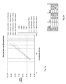
- FIG. 4 a is a chart showing the plotted relationship between total power consumption and pulse rate, with adaptive transducer impedance for each exemplary probe and operation-setup and with assumed transducer impedance as in previous practice.
- FIG. 4 b is a chart showing the plotted relationship between the pulser power consumption and pulse rate with adaptive transducer impedance for each specific exemplary probe and operation-setup specific.
- FIG. 5 is a schematic view of the preferred embodiment including elements providing pulse rate optimization for the PA system.
- FIG. 6 is a flow chart block diagram showing the steps and sub-modules of the Adaptive Impedance Calculator.
- FIG. 7 describes the Total Energy Pulse-rate Optimizer showing flow chart of the steps of seeking optimized pulse rate, with the true transducer impedance known, meeting total power consumption requirement.
- FIG. 8 delineates the Thermal Energy Pulse-rate Optimizer, showing the steps of seeking optimized pulse rate, with the true transducer impedance known, meeting both total power consumption requirement and the pulser thermal (power consumption) limit.
- FIG. 1 illustrates a conventional prior art circuitry for a typical circuitry for phased array probe pulser 10 .
- the conventional pulser-probe circuitry can be grouped into two portions, one comprises a transducer or probe 20 , the other portion embodies the whole pulser 10 , which further includes electronics such as resistors 12 , mosfet 14 , diodes 16 , analog switches 18 , etc.
- This typical pulser circuitry is also used as an exemplary pulser circuitry by the present disclosure.
- P pulser is the summation of the power lost within all discrete pulser elements, such as resistors 12 , mosfet 14 , diodes 16 , analog switches 18 , etc.
- Another principal involves the basic understanding that once a pulser circuitry, such as 10 and transducer circuit 20 are designed; there is an intrinsic physical limit to the total power consumption P total . It is widely known that, in general, higher the pulse-rate, higher the total power consumption. It is however, one of the objectives of the present disclosure to determine and quantify the relationship between the pulse rate and the total power consumption, with the true adaptive pulser impedance found using the method later described in this disclosure.
- Yet another aspect of the present disclosure is to examine the limit of the pulser power consumption imposed by the thermal limit of the pulser. It is widely known that any electronic circuitry has thermal limit and its corresponding limit to power consumption of the circuit.
- the power consumption of the pulser with the transducer impedance specific to the probe and pulser adaptive conditions (herein after referred to as “adaptive transducer impedance) is deduced and separated from the total power consumption.
- the pulser power consumption is calculated based on true measurement of the adaptive conditions including the adaptive value of the transducer impedance.
- the thermal limit on the pulser power consumption is then imposed on the pulse rate, which is another aspect of seeking optimization of the pulse rate.
- the optimized pulse rate is the highest pulse rate that meets the limit of total power consumption by both pulser and transducer, and the pulser power consumption with a limit imposed by the thermal limit of the pulser circuit.
- phased array NDT instrument For a given phased array NDT instrument, all the discrete elements found on a pulser circuit such as that of 10 are already known. Power consumption of each discrete element varies depending on various factors including voltage at power supply 30 , pulse width according to the setup of the phased array operation and the adaptive or operational value of transducer impedance. It is also known that one can use SPICE modeling to deduce the power consumption for all the discrete elements of the known pulser circuits.
- One novel aspect of the present disclosure is to provide a method to establish relationship (mathematical equations) between the power consumption lost inside pulser circuit 10 and the various factors affecting the power consumption, and subsequently finding the pulser power consumption using Eq. 1.
- SPICE is herein employed and its method is used to construct equations that model the power dissipation on all components in relation to various parameters such as voltage/pulse width/transducer impedance.
- SPICE is widely known and used for electronics simulation and modeling.
- the power of each component is computed by the SPICE simulator.
- an array of parameters are varied with a series of assumed values such as those for voltage, pulse width and transducer impedance. Tables exhibited in FIGS. 2 a , 2 b , 2 c and 2 d show an example of the data extracted from the SPICE simulation.
- power consumption of each circuit component of pulser 10 is simulated under the conditions when pulser voltage at power supply 30 is set to be 115 v and the pulse width set to be 50 ns, 100 ns, 200 ns and 500 ns, respectively.
- the power consumption of each component is simulated with result being listed.
- the simulation result for transducer power consumption (P transducer ) is 162 mW.
- the simulation result for resistor 1 ( 18 ) power consumption is 35.3 mW.
- V is the voltage at the power supply 30 , which is 115 Volt, known and given to the SPICE model in this example;
- Z eq is the equivalent impedance of pulser circuit 10 and the transducer circuit 20 .
- transducer impedance Z transducer is unknown, but are assumed as constant 50, 100, 200 and 400 ohms in the interpolation process of defining relationship between transducer impedance Z transducer and equivalent pulser impedance Z eq .
- FIGS. 2 b , 2 c and 2 d in which power supply voltage are all assumed to be 115 V and the pulse width are assumed to be 100 ns, 200 ns and 500 ns, respectively. Power consumptions of different discrete components are simulated by SPICE model. The total power consumption under each situation is calculated using Eq. 2. Then equivalent impedance of pulser 10 and transducer 20 is calculated using Eq. 3 under each situation. Subsequently, similar to the exhibition shown in FIG. 2 a , for each table shown in FIGS. 2 b , 2 c and 2 d , four pairs of Z transducer and Z eq are found and the values of which are ready to be used to establish relationship between Z transducer and Z eq .
- FIG. 3 a shows a curve fitting process establishing the relationship between Z transducer and Z eq for each specific phased array probe.
- FIG. 3 a Graphics shown in FIG. 3 a are four lines which are simple representation of the data obtained in the above simulation process with pairs of values for Z transducer and Z eq as exhibited in Tables 1 ⁇ 4 in FIGS. 2 a - 2 d for assumed pulse width of 50 ns, 100 ns, 200 ns and 500 ns, respectively.
- Curve fitting methods such as Logarithmic curve fitting known to those skilled in the art can be used to extract one equation for each group of data points for Z transducer and Z eq for each pulse width as follows.
- Z eq k 1 ln( Z transducer ) ⁇ k 2 Eq. 4
- transducer impedance are unknown but assumed constant (row one of Tables 1-4 in FIGS. 2 a ⁇ 2 d ), in order to establish relationship between Z eq and Z transducer .
- total power consumption can be obtained dynamically and the adaptive values of Z eq and Z transducer can be further determined from these measurements.
- the instant power consumption of transducer 20 can be dynamically deduced, which provides the basis to optimize the pulser pulse rate.
- the preferred embodiment includes the steps of constantly monitoring the output voltage V and the output current I at outflow at power supply 30 .
- P Total in Watt is the total power consumption expressed in Watt.
- P Total in Equ. 1 then equals to P Total in Watt when N ch is equal to one.
- the adaptive value of the transducer impedance is derived based on measurement of the specific pulser circuit.
- the task is moved onto providing guiding relationship between the power consumption and the pulse rate with established adaptive impedance for the given probe.
- FIG. 4 a depicts the process of finding the maximally allowed pulse rate (PRF) based on the limitation of total power consumption.
- PRF maximally allowed pulse rate
- the difference is shown between the curves for the probes with each with respective adaptive transducer impedance obtained based on specific probe circuit and measurement and the curve with the transducer impedance being assumed (diamond legend).
- the maximally allowed PRF for the assumed transducer impedance is about 4800 Hz using the previous practice.
- the values of optimal pulse rate range between 4000 and 8800 in Hz. This shows a clear advantage of using the presently disclosed method to determine the optimal pulse rate.
- pulse rate PRF is also limited by the power consumption within the pulser circuit.
- the relationship between pulse-rate PRF and the pulser power consumption based on adaptive transducer impedance is developed in the following.
- V transducer k 3 ln( Z transducer ) ⁇ k 4 Eq. 12
- P pulser P total - P transducer ⁇ ⁇ or Eq . ⁇ 13
- P pulser ( V 2 Z eq - V transducer 2 Z transducer ) * PulseWidth * PRF * N ch Eq . ⁇ 14
- FIG. 4 b Similar to the method described above related to FIG. 4 a for finding maximum pulse rate according to total power consumption limit, as seen in FIG. 4 b , the relationship between the pulser power consumption P pulser and the pulse rate (PRF) is plotted according to Eq. 14 for the adaptive transducer impedance for 50 ohms, 100 ohms, 200 ohms and 400 ohms, respectively.
- P pulser pulser power consumption
- PRF pulse rate
- the optimum pulse-rate is then established to be the lesser value of PRFs determined in FIGS. 4 a and 4 b , specifically for each probe.
- FIG. 5 The method as described above to calibrate the phased array system with the optimized pulse-rate is preferably implemented by a preferred embodiment embodying a phased array instrument 22 comprising one or more software modules which are executable by any PA digital processing circuits.
- Instrument 22 includes the elements that are included in an existing conventional PA instrument 22 a (not encircled), which typically includes a memory 3 , a data acquisition unit 4 and a data processor 9 a .
- the presently disclosed preferred embodiment further embodies a pulse rate optimizer 5 which is added to existing processor 9 a and form digital processor 9 for the preferred embodiment.
- Optimizer 5 can be part of the digital processor 9 or to be couple or loaded onto the existing data processor 9 a of an existing phased array inspection product.
- the pulse rate optimizer 5 includes an adaptive impedance calculator 6 , a total energy consumption pulse rate optimizer 7 and a pulser energy consumption pulse rate optimizer 8 as shown in FIG. 5 and further detailed in FIGS. 6 , 7 and 8 respectively.
- Pulse rate optimizer 8 is also called Thermal Limit Pulse-rate optimizer for the reasons provided in method description.
- FIG. 6 is a flowchart blocks depicting the sub-coding modules and/or steps embodying the adaptive impedance calculator 6 , which is turned on each time when a new probe is changed and engaged with PA instrument 22 .
- the pulse-rate optimizer receives instruction that PA system 22 needs a pulser calibration session.
- the adaptive impedance calculator records new configurations with a set of predetermined acquisition parameters.
- the acquisition parameters include those involved in Eq. 8, such as pulse width of the PA system.
- Nch is also included in the acquisition parameters, which is the number of transducer that is employed for the calibration and later inspection sessions.
- step 603 focal law is applied to test object via transducer (probe) 20 according to the configuration in step 602 .
- the following parameters from Eq. 8 are measured.
- step 605 total power consumption is calculated based on the measurement in step 604 and Eq. 8.
- step 607 adaptive pulser impedance Z eq is computed according to Eq. 3 and stored in a configuration file for the current usage of the instrument in step 608 .
- the configuration file can be resided within a memory of system 22 or 22 a.
- FIG. 7 depicting the sub-coding modules and/or steps embodying the total energy pulse-rate optimizer 7 , which is turned on each time when the system is adjusted with a new setup, such as a new pulse-width.
- step 701 optimizer 7 records a changed in new user setup for operational parameters such as pulse width or voltage.
- step 702 optimizer 7 starts the process of finding a new optimized pulse rate for the new setup parameters.
- step 702 optimizer 7 retrieves all the parameters from the user setup for pulser voltage, pulse width and number of transducer elements and the calculated adaptive impedance from step 608 .
- step 704 the optimizer 7 uses Eq. 8 and the process demonstrated in FIG. 4 a , and the given maximally available total power supply to find the optimized pulse rate PRF max .
- the value for PRF max is stored in step 705 .
- FIG. 8 depicting the sub-coding modules and/or steps embodying thermal limit or pulser energy pulse-rate optimizer (later short as Thermal Optimizer 8 ).
- Thermal Optimizer 8 is turned on each time when the system is adjusted with a new setup, such as a new pulse-width.
- thermal optimizer 8 records a changed in new user setup for operational parameters such as pulse width or voltage and retrieves predetermined k1 and k2 based obtained from SPICE model and curve fitting shown in FIG. 3 .
- thermal optimizer 8 computes adaptive Z transducer using Eq. 6 and Z eq from step 607 .
- thermal optimizer 8 retrieves predetermined k3 and k4 obtained from SPICE model and curve fitting in a process similar to the process shown in FIG. 3 and as explained in method description.
- V transducer is computed according to Eq. 12.
- the process calculates the power consumption by the pulser alone (not including consumption of the transducer) using Eq.
- thermal optimizer 8 determines if the pulser energy consumption has exceeded its thermal limit (given according to industry standard for electronic components for specific pulser circuit). If yes, Thermal Optimizer 8 decreases the PRF max and compute a new P pulser using Eq/13 and updates the new PRF max . If not, in step 812 , thermal optimizer uses the PRF max value obtained in step 705 .
Landscapes
- Physics & Mathematics (AREA)
- Health & Medical Sciences (AREA)
- Life Sciences & Earth Sciences (AREA)
- Chemical & Material Sciences (AREA)
- Analytical Chemistry (AREA)
- Biochemistry (AREA)
- General Health & Medical Sciences (AREA)
- General Physics & Mathematics (AREA)
- Immunology (AREA)
- Pathology (AREA)
- Ultra Sonic Daignosis Equipment (AREA)
Abstract
Description
P total =P pulser +P transducers Eq. 1
P total =P Res
-
- wherein, the power consumption of each element on the right-hand side of Eq. 2 is resulted from SPICE model simulation of pulser circuitry shown in
FIG. 1 , more particularly,- PRes
— 1, PRes— 2, PRes— 3, PRes— 4 are the power consumptions ofresistors - Pmosfet is the power consumption of
mosfet 14; - Pdiode
— 1 and Pdiode— 2 are the power consumptions ofdiodes
- PRes
- wherein, the power consumption of each element on the right-hand side of Eq. 2 is resulted from SPICE model simulation of pulser circuitry shown in
Z eq =k 1 ln(Z transducer)−k2 Eq. 4
Z eq=22.128 ln(Z transducer)−46.978 Eq. 5 for pulse width=50 ns
P TotalinWatt =V*I*DutyCycle*N ch Eq. 8
-
- wherein,
- DutyCycle=PulseWidth*PulseRate;
- Nch is the number of active pulsers;
- V is the voltage measured at
power supply 30; - I is the current measured at
power supply 30.
-
- wherein Vtransducer is the voltage measured between
pulser circuit 10 andtransducer 20 inFIG. 1 . - Ztransducer is the transducer impedance, the same as defined in previous discussions.
- wherein Vtransducer is the voltage measured between
V transducer =k 3 ln(Z transducer)−k 4 Eq. 12
Claims (19)
Z eq =k 1 ln(Z transducer)−k 2
Priority Applications (1)
| Application Number | Priority Date | Filing Date | Title |
|---|---|---|---|
| US13/360,175 US9080952B2 (en) | 2012-01-27 | 2012-01-27 | Method and a device of phased array inspection with pulse rate optimization |
Applications Claiming Priority (1)
| Application Number | Priority Date | Filing Date | Title |
|---|---|---|---|
| US13/360,175 US9080952B2 (en) | 2012-01-27 | 2012-01-27 | Method and a device of phased array inspection with pulse rate optimization |
Publications (2)
| Publication Number | Publication Date |
|---|---|
| US20130197841A1 US20130197841A1 (en) | 2013-08-01 |
| US9080952B2 true US9080952B2 (en) | 2015-07-14 |
Family
ID=48870994
Family Applications (1)
| Application Number | Title | Priority Date | Filing Date |
|---|---|---|---|
| US13/360,175 Active 2033-09-15 US9080952B2 (en) | 2012-01-27 | 2012-01-27 | Method and a device of phased array inspection with pulse rate optimization |
Country Status (1)
| Country | Link |
|---|---|
| US (1) | US9080952B2 (en) |
Families Citing this family (1)
| Publication number | Priority date | Publication date | Assignee | Title |
|---|---|---|---|---|
| CN113125561A (en) * | 2021-04-26 | 2021-07-16 | 合肥江丰电子材料有限公司 | Detection method of LCD (liquid Crystal display) planar target |
Citations (1)
| Publication number | Priority date | Publication date | Assignee | Title |
|---|---|---|---|---|
| US20100327880A1 (en) * | 2009-06-30 | 2010-12-30 | Orthosensor | Pulsed waveguide sensing device and method for measuring a parameter |
-
2012
- 2012-01-27 US US13/360,175 patent/US9080952B2/en active Active
Patent Citations (1)
| Publication number | Priority date | Publication date | Assignee | Title |
|---|---|---|---|---|
| US20100327880A1 (en) * | 2009-06-30 | 2010-12-30 | Orthosensor | Pulsed waveguide sensing device and method for measuring a parameter |
Non-Patent Citations (3)
| Title |
|---|
| Svilainis et al., Evaluation of the Ultrasonic Transducer Electrical Matching Performance, 2007, Ultragarsas, vol. 62, No. 4, pp. 16-21. * |
| Svilainis et al., Measurement of Complex Impedance of Ultrasonic Transducers, 2007, Ultragarsas, Nr. 1(62), pp. 26-29. * |
| Svilainis et al., Optimization of the Ultrasonic Excitation Stage, Jun. 23-26, 2008, Proceedings of the ITI 2008 30th International Conference on Information Technology Interfaces, Cavtat, Croatia, pp. 791-796. * |
Also Published As
| Publication number | Publication date |
|---|---|
| US20130197841A1 (en) | 2013-08-01 |
Similar Documents
| Publication | Publication Date | Title |
|---|---|---|
| US8192075B2 (en) | Method for performing ultrasonic testing | |
| Zhang et al. | Monte Carlo inversion of ultrasonic array data to map anisotropic weld properties | |
| Hoche et al. | Density, ultrasound velocity, acoustic impedance, reflection and absorption coefficient determination of liquids via multiple reflection method | |
| US7532992B2 (en) | Measuring apparatuses and methods of using them | |
| US11204291B2 (en) | Interface ultrasonic reflectivity-pressure relation curve establishment method and loading testbed | |
| CN114994175A (en) | Space coupling ultrasonic stress detection device and method for modal decomposition double-spectrum analysis | |
| CN111122085B (en) | Structure assembly quality evaluation method based on power distribution characteristics | |
| US11193912B2 (en) | Ultrasonic measurement apparatus and ultrasonic measurement method | |
| Alvarenga et al. | Monte Carlo uncertainty assessment of ultrasonic beam parameters from immersion transducers used to non-destructive testing | |
| US9243883B2 (en) | Apparatus and method for conducting and real-time application of EC probe calibration | |
| CN104165795B (en) | A kind of residue anti-bending bearing capacity assay method of ancient building wooden frame | |
| US9080952B2 (en) | Method and a device of phased array inspection with pulse rate optimization | |
| Jensen | Safety assessment of advanced imaging sequences II: Simulations | |
| Duxbury et al. | The effect of variation in phased array element performance for non-destructive evaluation (NDE) | |
| US20210364471A1 (en) | Method for Creating an Evaluation Table for an Ultrasonic Inspection and Method for Ultrasonic Inspection | |
| US10261054B2 (en) | Method for the non-destructive ultrasonic testing of a part by echo analysis | |
| JP5575157B2 (en) | Ultrasonic flaw detector, method and program | |
| CN113639804B (en) | Method and system for detecting quality of cable conduit | |
| US7617738B2 (en) | Method and apparatus for measuring flow rate of fluid | |
| CN115577552A (en) | A Simulation Method of Non-stationary Super-Gaussian Random Vibration Signal | |
| JP2018048830A5 (en) | ||
| CN207232088U (en) | A kind of container corrosion detection device | |
| Joneit et al. | Correction of eddy current measurements to obtain accordance with simulation results | |
| RU2784787C1 (en) | Method for eddy current control of wall thickness of metal non-magnetic pipes | |
| Dib et al. | Experimental validation of ultrasonic NDE simulation software |
Legal Events
| Date | Code | Title | Description |
|---|---|---|---|
| STCF | Information on status: patent grant |
Free format text: PATENTED CASE |
|
| MAFP | Maintenance fee payment |
Free format text: PAYMENT OF MAINTENANCE FEE, 4TH YEAR, LARGE ENTITY (ORIGINAL EVENT CODE: M1551); ENTITY STATUS OF PATENT OWNER: LARGE ENTITY Year of fee payment: 4 |
|
| AS | Assignment |
Owner name: OLYMPUS AMERICA INC., PENNSYLVANIA Free format text: MERGER;ASSIGNOR:OLYMPUS SCIENTIFIC SOLUTIONS AMERICAS INC.;REEL/FRAME:059327/0468 Effective date: 20160404 Owner name: OLYMPUS NDT INC., MASSACHUSETTS Free format text: ASSIGNMENT OF ASSIGNORS INTEREST;ASSIGNORS:SIMARD, CHRISTIAN;LAQUERRE, DENYS;REEL/FRAME:059327/0286 Effective date: 20120111 Owner name: OLYMPUS SCIENTIFIC SOLUTIONS AMERICAS INC., MASSACHUSETTS Free format text: CHANGE OF NAME;ASSIGNOR:OLYMPUS NDT INC.;REEL/FRAME:059327/0377 Effective date: 20140401 |
|
| MAFP | Maintenance fee payment |
Free format text: PAYMENT OF MAINTENANCE FEE, 8TH YEAR, LARGE ENTITY (ORIGINAL EVENT CODE: M1552); ENTITY STATUS OF PATENT OWNER: LARGE ENTITY Year of fee payment: 8 |
|
| AS | Assignment |
Owner name: EVIDENT SCIENTIFIC, INC., MASSACHUSETTS Free format text: CONFIRMATORY ASSIGNMENT;ASSIGNOR:OLYMPUS AMERICA INC.;REEL/FRAME:066143/0724 Effective date: 20231130 |