US9059120B2 - In-situ relaxation for improved CMOS product lifetime - Google Patents
In-situ relaxation for improved CMOS product lifetime Download PDFInfo
- Publication number
- US9059120B2 US9059120B2 US14/077,723 US201314077723A US9059120B2 US 9059120 B2 US9059120 B2 US 9059120B2 US 201314077723 A US201314077723 A US 201314077723A US 9059120 B2 US9059120 B2 US 9059120B2
- Authority
- US
- United States
- Prior art keywords
- field
- effect transistor
- well
- drain
- integrated circuit
- Prior art date
- Legal status (The legal status is an assumption and is not a legal conclusion. Google has not performed a legal analysis and makes no representation as to the accuracy of the status listed.)
- Expired - Fee Related, expires
Links
- 238000011065 in-situ storage Methods 0.000 title description 2
- 230000005669 field effect Effects 0.000 claims abstract description 88
- 238000000034 method Methods 0.000 claims abstract description 28
- 239000007795 chemical reaction product Substances 0.000 claims abstract description 6
- 239000000463 material Substances 0.000 claims description 24
- 239000004065 semiconductor Substances 0.000 claims description 22
- 239000012212 insulator Substances 0.000 claims description 15
- 239000000758 substrate Substances 0.000 claims description 13
- 230000008878 coupling Effects 0.000 claims description 7
- 238000010168 coupling process Methods 0.000 claims description 7
- 238000005859 coupling reaction Methods 0.000 claims description 7
- 230000005684 electric field Effects 0.000 claims description 4
- 238000002955 isolation Methods 0.000 description 22
- 239000002019 doping agent Substances 0.000 description 9
- 230000015556 catabolic process Effects 0.000 description 8
- 230000008569 process Effects 0.000 description 7
- VYPSYNLAJGMNEJ-UHFFFAOYSA-N Silicium dioxide Chemical compound O=[Si]=O VYPSYNLAJGMNEJ-UHFFFAOYSA-N 0.000 description 6
- 230000007547 defect Effects 0.000 description 6
- 238000006731 degradation reaction Methods 0.000 description 5
- 230000000694 effects Effects 0.000 description 5
- 238000009825 accumulation Methods 0.000 description 4
- 238000005229 chemical vapour deposition Methods 0.000 description 4
- 239000000615 nonconductor Substances 0.000 description 4
- XUIMIQQOPSSXEZ-UHFFFAOYSA-N Silicon Chemical compound [Si] XUIMIQQOPSSXEZ-UHFFFAOYSA-N 0.000 description 3
- 230000008859 change Effects 0.000 description 3
- 239000000470 constituent Substances 0.000 description 3
- 239000003989 dielectric material Substances 0.000 description 3
- 238000005530 etching Methods 0.000 description 3
- 229910052751 metal Inorganic materials 0.000 description 3
- 239000002184 metal Substances 0.000 description 3
- 230000000737 periodic effect Effects 0.000 description 3
- 229910052710 silicon Inorganic materials 0.000 description 3
- 239000010703 silicon Substances 0.000 description 3
- 239000000377 silicon dioxide Substances 0.000 description 3
- 239000000126 substance Substances 0.000 description 3
- ZOXJGFHDIHLPTG-UHFFFAOYSA-N Boron Chemical compound [B] ZOXJGFHDIHLPTG-UHFFFAOYSA-N 0.000 description 2
- OAICVXFJPJFONN-UHFFFAOYSA-N Phosphorus Chemical compound [P] OAICVXFJPJFONN-UHFFFAOYSA-N 0.000 description 2
- 229910052785 arsenic Inorganic materials 0.000 description 2
- RQNWIZPPADIBDY-UHFFFAOYSA-N arsenic atom Chemical compound [As] RQNWIZPPADIBDY-UHFFFAOYSA-N 0.000 description 2
- 238000000231 atomic layer deposition Methods 0.000 description 2
- 229910052796 boron Inorganic materials 0.000 description 2
- 239000000969 carrier Substances 0.000 description 2
- 238000004891 communication Methods 0.000 description 2
- 230000000295 complement effect Effects 0.000 description 2
- 239000011810 insulating material Substances 0.000 description 2
- 238000005468 ion implantation Methods 0.000 description 2
- 150000002500 ions Chemical class 0.000 description 2
- 238000001459 lithography Methods 0.000 description 2
- 229910044991 metal oxide Inorganic materials 0.000 description 2
- 150000004706 metal oxides Chemical class 0.000 description 2
- 229910052698 phosphorus Inorganic materials 0.000 description 2
- 239000011574 phosphorus Substances 0.000 description 2
- 238000005240 physical vapour deposition Methods 0.000 description 2
- 238000005498 polishing Methods 0.000 description 2
- 229910021420 polycrystalline silicon Inorganic materials 0.000 description 2
- 235000012239 silicon dioxide Nutrition 0.000 description 2
- 230000001960 triggered effect Effects 0.000 description 2
- 230000002411 adverse Effects 0.000 description 1
- 238000000429 assembly Methods 0.000 description 1
- 230000000712 assembly Effects 0.000 description 1
- 230000015572 biosynthetic process Effects 0.000 description 1
- -1 but not limited to Substances 0.000 description 1
- 239000002800 charge carrier Substances 0.000 description 1
- 229910052681 coesite Inorganic materials 0.000 description 1
- 239000004020 conductor Substances 0.000 description 1
- 229910052906 cristobalite Inorganic materials 0.000 description 1
- 239000013078 crystal Substances 0.000 description 1
- 238000000151 deposition Methods 0.000 description 1
- 230000006866 deterioration Effects 0.000 description 1
- 238000005516 engineering process Methods 0.000 description 1
- 229910052735 hafnium Inorganic materials 0.000 description 1
- VBJZVLUMGGDVMO-UHFFFAOYSA-N hafnium atom Chemical compound [Hf] VBJZVLUMGGDVMO-UHFFFAOYSA-N 0.000 description 1
- 229910000449 hafnium oxide Inorganic materials 0.000 description 1
- WIHZLLGSGQNAGK-UHFFFAOYSA-N hafnium(4+);oxygen(2-) Chemical compound [O-2].[O-2].[Hf+4] WIHZLLGSGQNAGK-UHFFFAOYSA-N 0.000 description 1
- 125000001475 halogen functional group Chemical group 0.000 description 1
- 230000006872 improvement Effects 0.000 description 1
- 238000002347 injection Methods 0.000 description 1
- 239000007924 injection Substances 0.000 description 1
- 238000009434 installation Methods 0.000 description 1
- 238000004519 manufacturing process Methods 0.000 description 1
- 230000007246 mechanism Effects 0.000 description 1
- 238000001465 metallisation Methods 0.000 description 1
- 238000012986 modification Methods 0.000 description 1
- 230000004048 modification Effects 0.000 description 1
- 229910021421 monocrystalline silicon Inorganic materials 0.000 description 1
- 238000006386 neutralization reaction Methods 0.000 description 1
- 238000000059 patterning Methods 0.000 description 1
- 238000000206 photolithography Methods 0.000 description 1
- 229920005591 polysilicon Polymers 0.000 description 1
- 239000000047 product Substances 0.000 description 1
- 230000004044 response Effects 0.000 description 1
- 229910021332 silicide Inorganic materials 0.000 description 1
- FVBUAEGBCNSCDD-UHFFFAOYSA-N silicide(4-) Chemical compound [Si-4] FVBUAEGBCNSCDD-UHFFFAOYSA-N 0.000 description 1
- 125000006850 spacer group Chemical group 0.000 description 1
- 229910052682 stishovite Inorganic materials 0.000 description 1
- 230000007704 transition Effects 0.000 description 1
- 238000003949 trap density measurement Methods 0.000 description 1
- 229910052905 tridymite Inorganic materials 0.000 description 1
Images


Classifications
-
- H—ELECTRICITY
- H01—ELECTRIC ELEMENTS
- H01L—SEMICONDUCTOR DEVICES NOT COVERED BY CLASS H10
- H01L21/00—Processes or apparatus adapted for the manufacture or treatment of semiconductor or solid state devices or of parts thereof
- H01L21/02—Manufacture or treatment of semiconductor devices or of parts thereof
- H01L21/04—Manufacture or treatment of semiconductor devices or of parts thereof the devices having potential barriers, e.g. a PN junction, depletion layer or carrier concentration layer
- H01L21/18—Manufacture or treatment of semiconductor devices or of parts thereof the devices having potential barriers, e.g. a PN junction, depletion layer or carrier concentration layer the devices having semiconductor bodies comprising elements of Group IV of the Periodic Table or AIIIBV compounds with or without impurities, e.g. doping materials
- H01L21/30—Treatment of semiconductor bodies using processes or apparatus not provided for in groups H01L21/20 - H01L21/26
- H01L21/326—Application of electric currents or fields, e.g. for electroforming
-
- H—ELECTRICITY
- H01—ELECTRIC ELEMENTS
- H01L—SEMICONDUCTOR DEVICES NOT COVERED BY CLASS H10
- H01L21/00—Processes or apparatus adapted for the manufacture or treatment of semiconductor or solid state devices or of parts thereof
- H01L21/70—Manufacture or treatment of devices consisting of a plurality of solid state components formed in or on a common substrate or of parts thereof; Manufacture of integrated circuit devices or of parts thereof
- H01L21/77—Manufacture or treatment of devices consisting of a plurality of solid state components or integrated circuits formed in, or on, a common substrate
- H01L21/78—Manufacture or treatment of devices consisting of a plurality of solid state components or integrated circuits formed in, or on, a common substrate with subsequent division of the substrate into plural individual devices
- H01L21/82—Manufacture or treatment of devices consisting of a plurality of solid state components or integrated circuits formed in, or on, a common substrate with subsequent division of the substrate into plural individual devices to produce devices, e.g. integrated circuits, each consisting of a plurality of components
- H01L21/822—Manufacture or treatment of devices consisting of a plurality of solid state components or integrated circuits formed in, or on, a common substrate with subsequent division of the substrate into plural individual devices to produce devices, e.g. integrated circuits, each consisting of a plurality of components the substrate being a semiconductor, using silicon technology
- H01L21/8232—Field-effect technology
- H01L21/8234—MIS technology, i.e. integration processes of field effect transistors of the conductor-insulator-semiconductor type
- H01L21/823437—MIS technology, i.e. integration processes of field effect transistors of the conductor-insulator-semiconductor type with a particular manufacturing method of the gate conductors, e.g. particular materials, shapes
-
- H—ELECTRICITY
- H01—ELECTRIC ELEMENTS
- H01L—SEMICONDUCTOR DEVICES NOT COVERED BY CLASS H10
- H01L21/00—Processes or apparatus adapted for the manufacture or treatment of semiconductor or solid state devices or of parts thereof
- H01L21/70—Manufacture or treatment of devices consisting of a plurality of solid state components formed in or on a common substrate or of parts thereof; Manufacture of integrated circuit devices or of parts thereof
- H01L21/77—Manufacture or treatment of devices consisting of a plurality of solid state components or integrated circuits formed in, or on, a common substrate
- H01L21/78—Manufacture or treatment of devices consisting of a plurality of solid state components or integrated circuits formed in, or on, a common substrate with subsequent division of the substrate into plural individual devices
- H01L21/82—Manufacture or treatment of devices consisting of a plurality of solid state components or integrated circuits formed in, or on, a common substrate with subsequent division of the substrate into plural individual devices to produce devices, e.g. integrated circuits, each consisting of a plurality of components
- H01L21/822—Manufacture or treatment of devices consisting of a plurality of solid state components or integrated circuits formed in, or on, a common substrate with subsequent division of the substrate into plural individual devices to produce devices, e.g. integrated circuits, each consisting of a plurality of components the substrate being a semiconductor, using silicon technology
- H01L21/8232—Field-effect technology
- H01L21/8234—MIS technology, i.e. integration processes of field effect transistors of the conductor-insulator-semiconductor type
- H01L21/823481—MIS technology, i.e. integration processes of field effect transistors of the conductor-insulator-semiconductor type isolation region manufacturing related aspects, e.g. to avoid interaction of isolation region with adjacent structure
-
- H—ELECTRICITY
- H01—ELECTRIC ELEMENTS
- H01L—SEMICONDUCTOR DEVICES NOT COVERED BY CLASS H10
- H01L21/00—Processes or apparatus adapted for the manufacture or treatment of semiconductor or solid state devices or of parts thereof
- H01L21/70—Manufacture or treatment of devices consisting of a plurality of solid state components formed in or on a common substrate or of parts thereof; Manufacture of integrated circuit devices or of parts thereof
- H01L21/77—Manufacture or treatment of devices consisting of a plurality of solid state components or integrated circuits formed in, or on, a common substrate
- H01L21/78—Manufacture or treatment of devices consisting of a plurality of solid state components or integrated circuits formed in, or on, a common substrate with subsequent division of the substrate into plural individual devices
- H01L21/82—Manufacture or treatment of devices consisting of a plurality of solid state components or integrated circuits formed in, or on, a common substrate with subsequent division of the substrate into plural individual devices to produce devices, e.g. integrated circuits, each consisting of a plurality of components
- H01L21/822—Manufacture or treatment of devices consisting of a plurality of solid state components or integrated circuits formed in, or on, a common substrate with subsequent division of the substrate into plural individual devices to produce devices, e.g. integrated circuits, each consisting of a plurality of components the substrate being a semiconductor, using silicon technology
- H01L21/8232—Field-effect technology
- H01L21/8234—MIS technology, i.e. integration processes of field effect transistors of the conductor-insulator-semiconductor type
- H01L21/823493—MIS technology, i.e. integration processes of field effect transistors of the conductor-insulator-semiconductor type with a particular manufacturing method of the wells or tubs, e.g. twin tubs, high energy well implants, buried implanted layers for lateral isolation [BILLI]
-
- H—ELECTRICITY
- H01—ELECTRIC ELEMENTS
- H01L—SEMICONDUCTOR DEVICES NOT COVERED BY CLASS H10
- H01L21/00—Processes or apparatus adapted for the manufacture or treatment of semiconductor or solid state devices or of parts thereof
- H01L21/70—Manufacture or treatment of devices consisting of a plurality of solid state components formed in or on a common substrate or of parts thereof; Manufacture of integrated circuit devices or of parts thereof
- H01L21/77—Manufacture or treatment of devices consisting of a plurality of solid state components or integrated circuits formed in, or on, a common substrate
- H01L21/78—Manufacture or treatment of devices consisting of a plurality of solid state components or integrated circuits formed in, or on, a common substrate with subsequent division of the substrate into plural individual devices
- H01L21/82—Manufacture or treatment of devices consisting of a plurality of solid state components or integrated circuits formed in, or on, a common substrate with subsequent division of the substrate into plural individual devices to produce devices, e.g. integrated circuits, each consisting of a plurality of components
- H01L21/822—Manufacture or treatment of devices consisting of a plurality of solid state components or integrated circuits formed in, or on, a common substrate with subsequent division of the substrate into plural individual devices to produce devices, e.g. integrated circuits, each consisting of a plurality of components the substrate being a semiconductor, using silicon technology
- H01L21/8232—Field-effect technology
- H01L21/8234—MIS technology, i.e. integration processes of field effect transistors of the conductor-insulator-semiconductor type
- H01L21/8238—Complementary field-effect transistors, e.g. CMOS
-
- H—ELECTRICITY
- H01—ELECTRIC ELEMENTS
- H01L—SEMICONDUCTOR DEVICES NOT COVERED BY CLASS H10
- H01L21/00—Processes or apparatus adapted for the manufacture or treatment of semiconductor or solid state devices or of parts thereof
- H01L21/70—Manufacture or treatment of devices consisting of a plurality of solid state components formed in or on a common substrate or of parts thereof; Manufacture of integrated circuit devices or of parts thereof
- H01L21/77—Manufacture or treatment of devices consisting of a plurality of solid state components or integrated circuits formed in, or on, a common substrate
- H01L21/78—Manufacture or treatment of devices consisting of a plurality of solid state components or integrated circuits formed in, or on, a common substrate with subsequent division of the substrate into plural individual devices
- H01L21/82—Manufacture or treatment of devices consisting of a plurality of solid state components or integrated circuits formed in, or on, a common substrate with subsequent division of the substrate into plural individual devices to produce devices, e.g. integrated circuits, each consisting of a plurality of components
- H01L21/84—Manufacture or treatment of devices consisting of a plurality of solid state components or integrated circuits formed in, or on, a common substrate with subsequent division of the substrate into plural individual devices to produce devices, e.g. integrated circuits, each consisting of a plurality of components the substrate being other than a semiconductor body, e.g. being an insulating body
-
- H—ELECTRICITY
- H01—ELECTRIC ELEMENTS
- H01L—SEMICONDUCTOR DEVICES NOT COVERED BY CLASS H10
- H01L27/00—Devices consisting of a plurality of semiconductor or other solid-state components formed in or on a common substrate
- H01L27/02—Devices consisting of a plurality of semiconductor or other solid-state components formed in or on a common substrate including semiconductor components specially adapted for rectifying, oscillating, amplifying or switching and having potential barriers; including integrated passive circuit elements having potential barriers
- H01L27/04—Devices consisting of a plurality of semiconductor or other solid-state components formed in or on a common substrate including semiconductor components specially adapted for rectifying, oscillating, amplifying or switching and having potential barriers; including integrated passive circuit elements having potential barriers the substrate being a semiconductor body
- H01L27/08—Devices consisting of a plurality of semiconductor or other solid-state components formed in or on a common substrate including semiconductor components specially adapted for rectifying, oscillating, amplifying or switching and having potential barriers; including integrated passive circuit elements having potential barriers the substrate being a semiconductor body including only semiconductor components of a single kind
- H01L27/085—Devices consisting of a plurality of semiconductor or other solid-state components formed in or on a common substrate including semiconductor components specially adapted for rectifying, oscillating, amplifying or switching and having potential barriers; including integrated passive circuit elements having potential barriers the substrate being a semiconductor body including only semiconductor components of a single kind including field-effect components only
- H01L27/088—Devices consisting of a plurality of semiconductor or other solid-state components formed in or on a common substrate including semiconductor components specially adapted for rectifying, oscillating, amplifying or switching and having potential barriers; including integrated passive circuit elements having potential barriers the substrate being a semiconductor body including only semiconductor components of a single kind including field-effect components only the components being field-effect transistors with insulated gate
- H01L27/092—Devices consisting of a plurality of semiconductor or other solid-state components formed in or on a common substrate including semiconductor components specially adapted for rectifying, oscillating, amplifying or switching and having potential barriers; including integrated passive circuit elements having potential barriers the substrate being a semiconductor body including only semiconductor components of a single kind including field-effect components only the components being field-effect transistors with insulated gate complementary MIS field-effect transistors
-
- H—ELECTRICITY
- H01—ELECTRIC ELEMENTS
- H01L—SEMICONDUCTOR DEVICES NOT COVERED BY CLASS H10
- H01L27/00—Devices consisting of a plurality of semiconductor or other solid-state components formed in or on a common substrate
- H01L27/02—Devices consisting of a plurality of semiconductor or other solid-state components formed in or on a common substrate including semiconductor components specially adapted for rectifying, oscillating, amplifying or switching and having potential barriers; including integrated passive circuit elements having potential barriers
- H01L27/12—Devices consisting of a plurality of semiconductor or other solid-state components formed in or on a common substrate including semiconductor components specially adapted for rectifying, oscillating, amplifying or switching and having potential barriers; including integrated passive circuit elements having potential barriers the substrate being other than a semiconductor body, e.g. an insulating body
- H01L27/1203—Devices consisting of a plurality of semiconductor or other solid-state components formed in or on a common substrate including semiconductor components specially adapted for rectifying, oscillating, amplifying or switching and having potential barriers; including integrated passive circuit elements having potential barriers the substrate being other than a semiconductor body, e.g. an insulating body the substrate comprising an insulating body on a semiconductor body, e.g. SOI
-
- H—ELECTRICITY
- H03—ELECTRONIC CIRCUITRY
- H03K—PULSE TECHNIQUE
- H03K3/00—Circuits for generating electric pulses; Monostable, bistable or multistable circuits
- H03K3/02—Generators characterised by the type of circuit or by the means used for producing pulses
- H03K3/353—Generators characterised by the type of circuit or by the means used for producing pulses by the use, as active elements, of field-effect transistors with internal or external positive feedback
- H03K3/356—Bistable circuits
- H03K3/356104—Bistable circuits using complementary field-effect transistors
-
- G—PHYSICS
- G01—MEASURING; TESTING
- G01R—MEASURING ELECTRIC VARIABLES; MEASURING MAGNETIC VARIABLES
- G01R31/00—Arrangements for testing electric properties; Arrangements for locating electric faults; Arrangements for electrical testing characterised by what is being tested not provided for elsewhere
- G01R31/26—Testing of individual semiconductor devices
- G01R31/2607—Circuits therefor
- G01R31/2621—Circuits therefor for testing field effect transistors, i.e. FET's
-
- G—PHYSICS
- G01—MEASURING; TESTING
- G01R—MEASURING ELECTRIC VARIABLES; MEASURING MAGNETIC VARIABLES
- G01R31/00—Arrangements for testing electric properties; Arrangements for locating electric faults; Arrangements for electrical testing characterised by what is being tested not provided for elsewhere
- G01R31/26—Testing of individual semiconductor devices
- G01R31/2642—Testing semiconductor operation lifetime or reliability, e.g. by accelerated life tests
Definitions
- the invention relates generally to integrated circuits and, in particular, to methods and assemblies for extending the useful lifetime of an integrated circuit.
- CMOS complementary metal oxide semiconductor
- Interface degradation may originate from an increase in trap density at device interfaces, such as interfaces with the gate dielectric layer, caused by voltage stress over time. Because of the trapping of charge carriers, the switching characteristics of the CMOS field-effect transistor can be changed.
- Another effect that may reduce the useful lifetime of CMOS field-effect transistors is the presence of mobile carriers in the gate dielectric layer. These mobile carriers trigger numerous physical damage processes that can drastically change the device electrical parameters over prolonged periods of operation. For example, damage accumulation can eventually cause the integrated circuit to fail by causing shifts in the threshold voltages of the CMOS field-effect transistors.
- a method for restoring an electrical parameter of a field-effect transistor in an integrated circuit.
- the method includes coupling a source, a drain, and a gate electrode of the field-effect transistor with ground.
- the method further includes applying a restoration voltage to a well beneath the field-effect transistor while the source, the drain, and the gate electrode of the field-effect transistor are coupled with ground.
- a structure in an embodiment of the invention, includes an integrated circuit with a field-effect transistor and a well beneath the field-effect transistor, a first power supply configured to supply a positive supply voltage and ground to the integrated circuit, and a second power supply configured to supply a restoration voltage to the integrated circuit.
- the field-effect transistor has a source, a drain, and a gate electrode.
- the structure further includes a switch having a first position coupling either the positive supply voltage or ground from the first power supply with the well during normal operation of the integrated circuit and a second position coupling the first restoration voltage from the second power supply with the well during a relaxation operation.
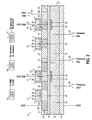
- FIG. 1 is a cross-sectional view of field-effect transistors wired with a relaxation circuit in accordance with an embodiment of the invention and biased in normal operation.
- FIG. 2 is a cross-sectional view similar to FIG. 1 in which the relaxation circuit is activated to subject the field-effect transistors to a relaxation operation.
- an integrated circuit 10 is comprised of a plurality of field-effect transistors 12 , 14 , 16 , 18 that are arranged at the top surface of a semiconductor-on-insulator (SOI) wafer 20 .
- SOI wafer 20 includes a device layer 22 , a buried insulator layer 24 , and a substrate 26 .
- the device layer 22 is separated from the substrate 26 by the intervening buried insulator layer 24 to provide electrical isolation and is considerably thinner than the substrate 26 .
- the thickness of the device layer 22 may range from about 3 nm to about 100 nm.
- the device layer 22 may have a thickness in the ultra-thin regime (i.e., 3 nm to 10 nm) suitable to manufacture fully-depleted SOI devices (FDSOI).
- the device layer 22 is supported on a top surface of the buried insulator layer 24 and is electrically insulated from the substrate 26 by the buried insulator layer 24 .
- the buried insulator layer 24 may be comprised of an electrical insulator and, in particular, may constitute a buried oxide layer that is comprised of silicon dioxide (e.g., SiO 2 ).
- FEOL front-end-of-line
- BEOL back-end-of-line
- the SOI wafer 20 is diced to define a plurality of chips.
- the integrated circuit 10 is included in one of the chips and the chip is packaged for installation in an electronic end product.
- the device layer 22 and the substrate 26 may be comprised of a semiconductor material, such as single crystal silicon or another single crystal semiconductor material that contains primarily silicon.
- An isolation well 28 is formed in the substrate 26 .
- the semiconductor material comprising the isolation well 28 and the semiconductor material comprising the remainder of the substrate 26 have opposite conductivity types.
- the isolation well 28 may comprise heavily-doped n-type semiconductor material applied as an in-situ doped epitaxial layer and the remainder of the substrate 26 may comprise lightly-doped p-type semiconductor material.
- a well 30 is comprised of sections of heavily-doped semiconductor material positioned within the isolation well 28 .
- the sections of the well 30 are formed by introducing an electrically-active dopant at selected locations in the isolation well 28 to counterdope the semiconductor material of isolation well 28 .
- the sections of well 30 may be formed in the substrate 26 by implanting ions comprising the dopant and with sufficient kinetic energy to penetrate through the device layer 22 and buried insulator layer 24 in the presence of a patterned sacrificial mask on the device layer 22 .
- the semiconductor material of the well 30 may comprise a p-type dopant selected from Group III of the Periodic Table (e.g., boron (B)) that is effective to impart p-type conductivity.
- the semiconductor material of the well 30 has an opposite conductivity type from the semiconductor material of the isolation well 28 .
- a well 32 is comprised of sections of heavily-doped semiconductor material positioned within the isolation well 28 .
- the well 32 is formed by introducing an electrically-active dopant at selected locations within each well 30 to counterdope the semiconductor material of well 30 .
- the sections of well 32 may be formed in the substrate 26 by implanting ions comprising the dopant and with sufficient kinetic energy to penetrate through the device layer 22 and buried insulator layer 24 in the presence of a patterned sacrificial mask on the device layer 22 .
- the semiconductor material of the well 32 may comprise an n-type dopant from Group V of the Periodic Table (e.g., phosphorus (P) or arsenic (As)) that is effective to impart n-type conductivity.
- the semiconductor material of well 32 has an opposite conductivity type from the semiconductor material of well 30 .
- the isolation well 28 electrically isolates the wells 30 , 32 from the remainder of the substrate 26 , and may have the same conductivity type as well 32 .
- Isolation regions 34 are provided in the device layer 22 .
- the isolation regions 34 may be formed by a shallow trench isolation (STI) technique that relies on lithography and dry etch processes to define trenches that reach in depth to the top surface 24 a of the buried insulator layer 24 , deposit an electrical insulator to fill the trenches, and planarize the electrical insulator relative to the top surface 22 a of the device layer 22 using, for example, chemical mechanical polishing (CMP).
- CMP chemical mechanical polishing
- the electrical insulator comprising the isolation regions 34 may be an oxide of silicon deposited by chemical vapor deposition (CVD).
- the isolation regions 34 may be formed by selectively removing the device layer 22 and subsequently allowing the opened spaces to be filled with insulating material after the complete formation of the device and during middle-end-of-line or back-end-of-line processing.
- the field-effect transistors 12 , 14 , 16 , 18 may be fabricated by complementary metal oxide semiconductor (CMOS) processes in front end of line (FEOL) processing, and the chip or die including the integrated circuit 10 may be categorized as a CMOS product.
- CMOS complementary metal oxide semiconductor
- Each of the field-effect transistors 12 , 14 , 16 , 18 includes a gate dielectric layer 36 and a gate electrode 38 that are positioned on the top surface 22 a of the device layer 22 as a gate structure with the gate dielectric layer 36 positioned between the gate electrode 38 and the device layer 22 .
- the gate electrode 38 may be comprised of a metal, a silicide, polycrystalline silicon (polysilicon), combinations of these materials, or any other appropriate conductor(s) deposited by physical vapor deposition (PVD), CVD, etc.
- the gate dielectric layer 36 may be comprised of any suitable dielectric or insulating material including, but not limited to, silicon dioxide, silicon oxynitride, a high-k dielectric material such as hafnium oxide or hafnium oxynitride, or layered combinations of these dielectric materials, deposited by CVD, atomic layer deposition (ALD), etc.
- the gate dielectric layer 36 and gate electrode 38 may be formed from a layer stack of their constituent materials applied on the top surface 22 a of the device layer 22 , and then patterning using photolithography and etching processes.
- the etching process which may be a wet chemical etch or a dry etch, may rely on one or more etch chemistries that remove the constituent materials selective to (i.e., at a higher etch rate than) the material constituting the device layer 22 .
- Non-conductive spacers 37 may be formed on the exterior sidewalls of each gate dielectric layer 36 and gate electrode 38 .
- a gate structure may be formed by depositing a dielectric layer, polishing the dielectric layer to expose the gate electrode 38 , removing the gate electrode 38 with a wet chemical etch, and then refilling the vacant space with appropriate metal layers to re-define the gate electrode 38 .
- Each of the field-effect transistors 12 , 14 , 16 , 18 includes a source 40 and a drain 42 formed in the device layer 22 .
- the source 40 and drain 42 of field-effect transistors 12 , 14 may have an opposite conductivity type from the source 40 and drain 42 of field-effect transistors 16 , 18 .
- source 40 and drain 42 of field-effect transistors 12 , 14 may comprise semiconductor material of the device layer 22 that is heavily doped by masked ion implantation with an n-type dopant (e.g., phosphorus (P) or arsenic (As)).
- P phosphorus
- As arsenic
- source 40 and drain 42 of field-effect transistors 16 , 18 may comprise semiconductor material of the device layer 22 that is heavily doped by masked ion implantation with a p-type dopant (e.g., boron (B)).
- the source 40 and drain 42 may be formed by epitaxial growth in the presence of the appropriate (n-type or p-type) dopant.
- the source 40 and drain 42 of the field-effect transistors 12 , 14 , 16 , 18 may be raised but, even if raised, will include a portion that is disposed in the device layer 22 .
- a channel 44 is defined in the device layer 22 between each source-drain pair.
- the field-effect transistors 12 , 14 , 16 , 18 may include other components such as halo regions, lightly-doped drain (LDD) regions, etc. in the device layer 22 .
- LDD lightly-doped drain
- the regions of well 32 may define backgates for the field-effect transistor 12 and the field-effect transistor 16 . These backgates may be biased to either lower or raise the conduction band in the channel 44 of the field-effect transistors 12 , 16 relative to its Fermi level and thereby decrease or increase the threshold voltage, V T , of the field-effect transistors 12 and 16 .
- the threshold voltage of the field-effect transistor 12 and the threshold voltage of the field-effect transistor 16 may each be adjusted independent of its channel doping with the respective backgate.
- the field-effect transistors 12 , 14 may be of the same type (e.g., NMOS transistors) and characterized by different threshold voltages due to the work function of the backgate, and the field-effect transistors 16 , 18 may be of the same type (e.g., PMOS transistors) and characterized by different threshold voltages due to the work function of the backgate.
- the substrate 26 beneath isolation well 28 and the well 30 may be coupled with the negative supply voltage (Vss) or ground (GND) of a power supply 50 .
- the isolation well 28 and the well 32 may be coupled with the positive supply voltage (Vdd) of the power supply 50 .
- the sources 40 of the field-effect transistors 12 , 14 , 16 , 18 may be coupled with ground (GND) of the power supply 50 and the drains 42 of the field-effect transistors 12 , 14 , 16 , 18 may be coupled with the positive supply voltage (Vdd) of the power supply 50 .
- the gate electrodes 38 of the field-effect transistors 12 , 14 , 16 , 18 are alternatively coupled with one or the other of the positive supply voltage (Vdd) or ground (GND) from inputs 52 , 54 coupled with the power supply 50 to provide low-to-high and high-to-low transitions at the gate electrodes 38 .
- the gate-source voltage, drain-source voltage and source-bulk voltage of the field-effect transistors 12 , 14 may all be positive during normal operation.
- the gate-source voltage, drain-source voltage and source-bulk voltage of the field-effect transistors 16 , 18 may all be negative during normal operation.
- the operating requirements of the integrated circuit 10 apply stress on the field-effect transistors 12 , 14 , 16 , 18 .
- the field-effect transistors 12 , 14 , 16 , 18 may degrade in performance during the device operation and may not retain their original electrical parameters.
- Degradation mechanisms may include, but are not limited to, charge accumulation in the gate dielectric layer 36 of the field-effect transistors 12 , 14 , 16 , 18 and the generation of traps at the interface between the gate dielectric layer 36 and device layer 22 .
- These defects 56 can be generated by phenomena such as negative-bias temperature instability, hot carrier injection, etc.
- the defects 56 can increase leakage current through the gate dielectric layer 36 , change observable transistor electrical parameters such as the threshold voltage, saturation current, and drain current, or may even result in device failure due to dielectric breakdown. High switching activity or a high frequency of operation for the field-effect transistors 12 , 14 , 16 , 18 may accelerate defect accumulation.
- the relaxation operation is configured to extend the useful lifetime of the field-effect transistors 12 , 14 , 16 , 18 and the integrated circuit 10 including the field-effect transistors 12 , 14 , 16 , 18 by alleviating performance and reliability problems potentially arising from the defects 56 .
- a relaxation circuit comprises switches 58 , 60 , 62 , 64 that are configurable to change the biasing of the isolation well 28 , the wells 30 , 32 , and the drains 42 of the field-effect transistors 16 , 18 away from the biasing conditions that exist under normal operation in order to perform a relaxation operation.
- the switches 58 , 60 , 62 , 64 may comprise field-effect transistors similar to field-effect transistors 12 , 14 , 16 , 18 .
- the switches 58 , 60 , 62 , 64 are used in conjunction with the power supply 50 , which is capable of producing the positive supply voltage (Vdd) and supplying ground (GND), and a power supply 66 configured to produce a positive restoration voltage (+Vrestore) and a negative restoration voltage ( ⁇ Vrestore).
- the positive restoration voltage (+Vrestore) and negative restoration voltage ( ⁇ Vrestore) have opposite polarity.
- the magnitudes of the positive restoration voltage (+Vrestore) and the negative restoration voltage ( ⁇ Vrestore) may be equal, the absolute value of the positive restoration voltage (+Vrestore) may be greater than the absolute value of the negative restoration voltage ( ⁇ Vrestore), or the absolute value of the positive restoration voltage (+Vrestore) may be less than the absolute value of the negative restoration voltage ( ⁇ Vrestore).
- the voltages are chosen to avoid forward-biasing the junctions of the wells 28 , 30 , 32 , and causing breakdown.
- Switch 58 is configured to couple the isolation well 28 with the positive supply voltage (Vdd) during normal operation of the integrated circuit 10 and with the positive restoration voltage (+Vrestore) during the relaxation operation.
- switch 58 has a position ( FIG. 1 ) in which the isolation well 28 is coupled with the positive supply voltage (Vdd) and another position ( FIG. 2 ) in which the isolation well 28 is coupled with the positive restoration voltage (+Vrestore).
- Switch 60 is configured to couple the well 30 with ground (GND) during normal operation of the integrated circuit 10 and with the positive restoration voltage (+Vrestore) during the relaxation operation.
- switch 60 has a position ( FIG. 1 ) in which the well 30 is coupled with ground (GND) and another position ( FIG. 2 ) in which the well 30 is coupled with the positive restoration voltage (+Vrestore).
- Switch 62 is configured to couple the well 32 with the positive supply voltage (Vdd) during normal operation of the integrated circuit 10 and with the negative restoration voltage ( ⁇ Vrestore) during the relaxation operation.
- switch 62 has a position ( FIG. 1 ) in which the well 32 is coupled with the positive supply voltage (Vdd) and another position ( FIG. 2 ) in which the well 32 is coupled with the negative restoration voltage ( ⁇ Vrestore).
- Switch 64 is configured to couple the drains 42 of the field-effect transistors 16 , 18 with the positive supply voltage (Vdd) during normal operation of the integrated circuit 10 and with ground (GND) during the relaxation operation.
- switch 64 has a position ( FIG. 1 ) in which the drains 42 of the field-effect transistors 16 , 18 are coupled with the positive supply voltage (Vdd) and another position ( FIG. 2 ) in which the drains 42 of the field-effect transistors 16 , 18 are coupled with ground (GND).
- a control circuit 70 is coupled in communication with the switches 58 , 60 , 62 , 64 and is configured to be activated to select switch positions to provide biasing for normal operation for the integrated circuit 10 ( FIG. 1 ) or biasing for a relaxation operation for the integrated circuit 10 ( FIG. 2 ).
- the control circuit 70 may also be coupled in communication with the power supply 66 and may be configured to cause the power supply 66 to be energized to provide the restoration voltages only when performing the relaxation operation.
- the control circuit 70 may be comprised of on-chip circuitry located on the chip that includes the integrated circuit 10 . Alternatively, the control circuit 70 may be comprised of off-chip circuitry.
- the control circuit 70 may be configured to monitor the integrated circuit 10 for detecting any deterioration in the electrical parameters characterizing the field-effect transistors 12 , 14 , 16 , 18 .
- the switches 58 , 60 , 62 , 64 and control circuit 70 may be fabricated using the device layer 22 of the SOI wafer 20 during FEOL processing.
- the chip may also comprise an interconnect structure that is configured to communicate signals to the field-effect transistors 12 , 14 , 16 , 18 of the integrated circuit 10 and to provide the power and ground connections of the integrated circuit 10 with the power supplies 50 , 66 .
- the interconnect structure which may be fabricated during BEOL processing by, for example, damascene processes, includes wiring layers comprised of metal features embedded in a dielectric layer. The metallization levels of the interconnect structure may be formed by lithography and etching techniques characteristic of damascene processes associated with BEOL processing.
- the switches 58 , 60 , 62 , 64 and field-effect transistors 12 , 14 , 16 , 18 may be coupled by wiring of the interconnect structure with the power supplies 50 , 66 .
- the integrated circuit 10 is depicted with a biasing scheme for performing a relaxation operation to extend the useful lifetime of the integrated circuit 10 .
- a decision may be made to perform the relaxation procedure to recover the initial electrical parameters of the field-effect transistors 12 , 14 , 16 , 18 of the integrated circuit 10 .
- the control circuit 70 actuates the switches 58 , 60 , 62 , 64 to direct power from the power supply 66 as needed for the relaxation operation.
- the relaxation operation can be either manually triggered or automatically triggered.
- the triggering decision may be based upon observations, such as sensing or detecting degradation of the electrical parameters of the field-effect transistors 12 , 14 , 16 , 18 of the integrated circuit 10 .
- the relaxation operation may be automatically scheduled to occur at intervals, such as periodic intervals.
- Parameters for the operation of the power supply 66 that may be selected with instructions or programmed settings include, but are not limited to, duration and frequency for the relaxation operation.
- the power supply 66 may bias the field-effect transistors 12 , 14 , 16 , 18 of the integrated circuit 10 with restoration voltages that are predicted, calculated, or empirically determined to alleviate at least a significant fraction, if not substantially all, of the defects 56 and restore the initial electrical parameters.
- the biases are supplied over a time duration adequate to impart a desired relaxation effect to the field-effect transistors 12 , 14 , 16 , 18 .
- the time duration of a relaxation operation may be fixed in length (e.g., restoration voltages applied for a given time in response to a command to execute a relaxation operation), controlled by explicit start-anneal and stop-anneal commands, or programmed into a control register within the control circuit 70 .
- Normal circuit operation may be disabled by grounding the supply potential, i.e., disabling the positive supply voltage (Vdd) at the power supply 50 .
- Vdd positive supply voltage
- the isolation well 28 and the well 30 are coupled by the actuation of switches 58 , 60 with a positive restoration voltage (+Vrestore) and the well 32 is coupled by the actuation of switch 62 with a negative restoration voltage ( ⁇ Vrestore).
- the magnitude of the restoration voltages is limited only by the breakdown and leakage of the wells 30 , 32 , and the switches 58 , 60 , 62 , 64 to switch between operating mode and relaxation mode.
- the gate electrodes 38 of the field-effect transistors 12 , 14 , 16 , 18 are coupled by the inputs 52 , 54 with ground (GND) and the drains 42 of the field-effect transistors 16 , 18 are coupled with ground (GND).
- the coupling of the sources 40 of the field-effect transistors 12 , 14 with ground (GND) is unchanged.
- the voltages at the gate electrode 38 , the source 40 , and the drain 42 of each of the field-effect transistors 12 , 14 , 16 , 18 are set to a zero potential reference, the well 30 beneath the field-effect transistors 12 , 14 is positively biased relative to the zero potential reference at their gate electrode 38 , the source 40 , and the drain 42 , and the well 32 beneath the field-effect transistors 16 , 18 is negatively biased relative to the zero potential reference at their gate electrode 38 , the source 40 , and the drain 42 .
- the gate-source voltage, drain-source voltage and source-bulk voltage of the field-effect transistors 12 , 14 , 16 , 18 are null (i.e., neither negative nor positive) during the relaxation operation.
- the biasing of the relaxation operation creates an electric field at field-effect transistors 12 , 14 that is directed from the channel 44 and well 30 toward the gate electrode 38 .
- the biasing of the relaxation operation creates an electric field at field-effect transistors 16 , 18 that is directed from the gate electrode 38 toward the channel 44 and well 32 .
- the junctions of the field-effect transistors 12 , 14 , 16 , 18 are not forward biased because the wells 30 , 32 are dielectrically isolated from the sources 40 and drains 42 by the buried insulator layer 24 between the wells 30 , 32 and the field-effect transistors 12 , 14 , 16 , 18 .
- the detrapping and neutralization of accumulated charge in the gate dielectric layer 36 and at its interfaces is enhanced by performing the relaxation operation.
- a feature may be “connected” or “coupled” to or with another element may be directly connected to or coupled with the other element or, instead, one or more intervening elements may be present.
- a feature may be “directly connected” or “directly coupled” to another element if intervening elements are absent.
- a feature may be “indirectly connected” or “indirectly coupled” to another element if at least one intervening element is present.
Landscapes
- Engineering & Computer Science (AREA)
- Power Engineering (AREA)
- Physics & Mathematics (AREA)
- Condensed Matter Physics & Semiconductors (AREA)
- General Physics & Mathematics (AREA)
- Computer Hardware Design (AREA)
- Microelectronics & Electronic Packaging (AREA)
- Manufacturing & Machinery (AREA)
- Metal-Oxide And Bipolar Metal-Oxide Semiconductor Integrated Circuits (AREA)
Abstract
Description
Claims (11)
Priority Applications (1)
| Application Number | Priority Date | Filing Date | Title |
|---|---|---|---|
| US14/077,723 US9059120B2 (en) | 2013-11-12 | 2013-11-12 | In-situ relaxation for improved CMOS product lifetime |
Applications Claiming Priority (1)
| Application Number | Priority Date | Filing Date | Title |
|---|---|---|---|
| US14/077,723 US9059120B2 (en) | 2013-11-12 | 2013-11-12 | In-situ relaxation for improved CMOS product lifetime |
Publications (2)
| Publication Number | Publication Date |
|---|---|
| US20150132862A1 US20150132862A1 (en) | 2015-05-14 |
| US9059120B2 true US9059120B2 (en) | 2015-06-16 |
Family
ID=53044119
Family Applications (1)
| Application Number | Title | Priority Date | Filing Date |
|---|---|---|---|
| US14/077,723 Expired - Fee Related US9059120B2 (en) | 2013-11-12 | 2013-11-12 | In-situ relaxation for improved CMOS product lifetime |
Country Status (1)
| Country | Link |
|---|---|
| US (1) | US9059120B2 (en) |
Families Citing this family (2)
| Publication number | Priority date | Publication date | Assignee | Title |
|---|---|---|---|---|
| US10090674B2 (en) * | 2015-09-21 | 2018-10-02 | Silicon Laboratories Inc. | Maximum supply voltage selection |
| JP2019029558A (en) * | 2017-08-01 | 2019-02-21 | ソニーセミコンダクタソリューションズ株式会社 | Transistor and electronic equipment |
Citations (8)
| Publication number | Priority date | Publication date | Assignee | Title |
|---|---|---|---|---|
| US5978277A (en) | 1998-04-06 | 1999-11-02 | Aplus Flash Technology, Inc. | Bias condition and X-decoder circuit of flash memory array |
| US5982225A (en) * | 1997-08-06 | 1999-11-09 | International Business Machines Corporation | Hot electron compensation for improved MOS transistor reliability |
| US5999455A (en) | 1998-06-12 | 1999-12-07 | Macronix International Co., Ltd. | Channel FN program/erase recovery scheme |
| US6841445B2 (en) | 1996-09-30 | 2005-01-11 | Sgs-Thomson Microelectronics S.R.L. | Method of making floating gate non-volatile memory cell with low erasing voltage having double layer gate dielectric |
| US7002397B2 (en) | 1999-01-26 | 2006-02-21 | Renesas Technology Corp. | Method of setting back bias of MOS circuit, and MOS integrated circuit |
| US20110001184A1 (en) | 2008-02-19 | 2011-01-06 | Francois Andrieu | Method of adjusting the threshold voltage of a transistor by a buried trapping layer |
| US20120281481A1 (en) | 2011-05-02 | 2012-11-08 | Macronix International Co., Ltd. | Thermally assisted dielectric charge trapping flash |
| US8422322B2 (en) | 2008-01-24 | 2013-04-16 | International Business Machines Corporation | Self-repair integrated circuit and repair method |
-
2013
- 2013-11-12 US US14/077,723 patent/US9059120B2/en not_active Expired - Fee Related
Patent Citations (8)
| Publication number | Priority date | Publication date | Assignee | Title |
|---|---|---|---|---|
| US6841445B2 (en) | 1996-09-30 | 2005-01-11 | Sgs-Thomson Microelectronics S.R.L. | Method of making floating gate non-volatile memory cell with low erasing voltage having double layer gate dielectric |
| US5982225A (en) * | 1997-08-06 | 1999-11-09 | International Business Machines Corporation | Hot electron compensation for improved MOS transistor reliability |
| US5978277A (en) | 1998-04-06 | 1999-11-02 | Aplus Flash Technology, Inc. | Bias condition and X-decoder circuit of flash memory array |
| US5999455A (en) | 1998-06-12 | 1999-12-07 | Macronix International Co., Ltd. | Channel FN program/erase recovery scheme |
| US7002397B2 (en) | 1999-01-26 | 2006-02-21 | Renesas Technology Corp. | Method of setting back bias of MOS circuit, and MOS integrated circuit |
| US8422322B2 (en) | 2008-01-24 | 2013-04-16 | International Business Machines Corporation | Self-repair integrated circuit and repair method |
| US20110001184A1 (en) | 2008-02-19 | 2011-01-06 | Francois Andrieu | Method of adjusting the threshold voltage of a transistor by a buried trapping layer |
| US20120281481A1 (en) | 2011-05-02 | 2012-11-08 | Macronix International Co., Ltd. | Thermally assisted dielectric charge trapping flash |
Also Published As
| Publication number | Publication date |
|---|---|
| US20150132862A1 (en) | 2015-05-14 |
Similar Documents
| Publication | Publication Date | Title |
|---|---|---|
| CN107425057B (en) | Semiconductor structure including transistor having gate electrode region in substrate and method of forming the same | |
| CN103151353B (en) | The metal gates parts of semiconductor element | |
| US9406669B2 (en) | Method and structure for vertical tunneling field effect transistor and planar devices | |
| CN102456579A (en) | Semiconductor device having localized extremely thin silicon on insulator channel region | |
| CN103035725A (en) | Strapped dual-gate vdmos device | |
| US9153684B2 (en) | Semiconductor fuses in a semiconductor device comprising metal gates | |
| US9502564B2 (en) | Fully depleted device with buried insulating layer in channel region | |
| US20160351699A1 (en) | Field-effect transistors with body dropdowns | |
| US20120267724A1 (en) | Mos semiconductor device and methods for its fabrication | |
| US20190051565A1 (en) | Cmos devices and manufacturing method thereof | |
| US20090065817A1 (en) | Dielectric spacer removal | |
| US10083959B2 (en) | Semiconductor device structure and method for forming the same | |
| US6930357B2 (en) | Active SOI structure with a body contact through an insulator | |
| KR100763230B1 (en) | Buried well for semiconductor devices | |
| US9059120B2 (en) | In-situ relaxation for improved CMOS product lifetime | |
| CN102867750B (en) | Mosfet and manufacturing method thereof | |
| US9379028B2 (en) | SOI CMOS structure having programmable floating backplate | |
| US9054221B2 (en) | Semiconductor device with a common back gate isolation region and method for manufacturing the same | |
| US8716799B2 (en) | Mosfet | |
| US20070166948A1 (en) | Buried silicon dioxide / silicon nitride bi-layer insulators and methods of fabricating the same | |
| US11764060B2 (en) | Field-effect transistors with a body pedestal | |
| US11195935B2 (en) | Semiconductor device with novel spacer structures having novel configurations | |
| US10580863B2 (en) | Transistor element with reduced lateral electrical field | |
| US10170315B2 (en) | Semiconductor device having local buried oxide | |
| TW202414693A (en) | Trigger silicon controlled rectifier |
Legal Events
| Date | Code | Title | Description |
|---|---|---|---|
| AS | Assignment |
Owner name: INTERNATIONAL BUSINESS MACHINES CORPORATION, NEW Y Free format text: ASSIGNMENT OF ASSIGNORS INTEREST;ASSIGNORS:HOOK, TERENCE B.;SCHNABEL, CHRISTOPHER M.;SHERONY, MELANIE J.;SIGNING DATES FROM 20131105 TO 20131111;REEL/FRAME:031585/0027 |
|
| STCF | Information on status: patent grant |
Free format text: PATENTED CASE |
|
| AS | Assignment |
Owner name: GLOBALFOUNDRIES U.S. 2 LLC, NEW YORK Free format text: ASSIGNMENT OF ASSIGNORS INTEREST;ASSIGNOR:INTERNATIONAL BUSINESS MACHINES CORPORATION;REEL/FRAME:036550/0001 Effective date: 20150629 |
|
| AS | Assignment |
Owner name: GLOBALFOUNDRIES INC., CAYMAN ISLANDS Free format text: ASSIGNMENT OF ASSIGNORS INTEREST;ASSIGNORS:GLOBALFOUNDRIES U.S. 2 LLC;GLOBALFOUNDRIES U.S. INC.;REEL/FRAME:036779/0001 Effective date: 20150910 |
|
| AS | Assignment |
Owner name: WILMINGTON TRUST, NATIONAL ASSOCIATION, DELAWARE Free format text: SECURITY AGREEMENT;ASSIGNOR:GLOBALFOUNDRIES INC.;REEL/FRAME:049490/0001 Effective date: 20181127 |
|
| FEPP | Fee payment procedure |
Free format text: MAINTENANCE FEE REMINDER MAILED (ORIGINAL EVENT CODE: REM.); ENTITY STATUS OF PATENT OWNER: LARGE ENTITY |
|
| LAPS | Lapse for failure to pay maintenance fees |
Free format text: PATENT EXPIRED FOR FAILURE TO PAY MAINTENANCE FEES (ORIGINAL EVENT CODE: EXP.); ENTITY STATUS OF PATENT OWNER: LARGE ENTITY |
|
| STCH | Information on status: patent discontinuation |
Free format text: PATENT EXPIRED DUE TO NONPAYMENT OF MAINTENANCE FEES UNDER 37 CFR 1.362 |
|
| FP | Lapsed due to failure to pay maintenance fee |
Effective date: 20190616 |
|
| AS | Assignment |
Owner name: GLOBALFOUNDRIES INC., CAYMAN ISLANDS Free format text: RELEASE BY SECURED PARTY;ASSIGNOR:WILMINGTON TRUST, NATIONAL ASSOCIATION;REEL/FRAME:054636/0001 Effective date: 20201117 |
|
| AS | Assignment |
Owner name: GLOBALFOUNDRIES U.S. INC., NEW YORK Free format text: RELEASE BY SECURED PARTY;ASSIGNOR:WILMINGTON TRUST, NATIONAL ASSOCIATION;REEL/FRAME:056987/0001 Effective date: 20201117 |