US9054497B2 - Quantum cascade lasers with improved performance using interface roughness scattering - Google Patents
Quantum cascade lasers with improved performance using interface roughness scattering Download PDFInfo
- Publication number
- US9054497B2 US9054497B2 US13/624,330 US201213624330A US9054497B2 US 9054497 B2 US9054497 B2 US 9054497B2 US 201213624330 A US201213624330 A US 201213624330A US 9054497 B2 US9054497 B2 US 9054497B2
- Authority
- US
- United States
- Prior art keywords
- scattering
- ifr
- laser level
- laser
- barrier
- Prior art date
- Legal status (The legal status is an assumption and is not a legal conclusion. Google has not performed a legal analysis and makes no representation as to the accuracy of the status listed.)
- Expired - Fee Related, expires
Links
Images


Classifications
-
- H—ELECTRICITY
- H01—ELECTRIC ELEMENTS
- H01S—DEVICES USING THE PROCESS OF LIGHT AMPLIFICATION BY STIMULATED EMISSION OF RADIATION [LASER] TO AMPLIFY OR GENERATE LIGHT; DEVICES USING STIMULATED EMISSION OF ELECTROMAGNETIC RADIATION IN WAVE RANGES OTHER THAN OPTICAL
- H01S5/00—Semiconductor lasers
- H01S5/20—Structure or shape of the semiconductor body to guide the optical wave ; Confining structures perpendicular to the optical axis, e.g. index or gain guiding, stripe geometry, broad area lasers, gain tailoring, transverse or lateral reflectors, special cladding structures, MQW barrier reflection layers
- H01S5/22—Structure or shape of the semiconductor body to guide the optical wave ; Confining structures perpendicular to the optical axis, e.g. index or gain guiding, stripe geometry, broad area lasers, gain tailoring, transverse or lateral reflectors, special cladding structures, MQW barrier reflection layers having a ridge or stripe structure
- H01S5/223—Buried stripe structure
- H01S5/2231—Buried stripe structure with inner confining structure only between the active layer and the upper electrode
-
- H—ELECTRICITY
- H01—ELECTRIC ELEMENTS
- H01S—DEVICES USING THE PROCESS OF LIGHT AMPLIFICATION BY STIMULATED EMISSION OF RADIATION [LASER] TO AMPLIFY OR GENERATE LIGHT; DEVICES USING STIMULATED EMISSION OF ELECTROMAGNETIC RADIATION IN WAVE RANGES OTHER THAN OPTICAL
- H01S5/00—Semiconductor lasers
- H01S5/20—Structure or shape of the semiconductor body to guide the optical wave ; Confining structures perpendicular to the optical axis, e.g. index or gain guiding, stripe geometry, broad area lasers, gain tailoring, transverse or lateral reflectors, special cladding structures, MQW barrier reflection layers
- H01S5/2004—Confining in the direction perpendicular to the layer structure
-
- H—ELECTRICITY
- H01—ELECTRIC ELEMENTS
- H01S—DEVICES USING THE PROCESS OF LIGHT AMPLIFICATION BY STIMULATED EMISSION OF RADIATION [LASER] TO AMPLIFY OR GENERATE LIGHT; DEVICES USING STIMULATED EMISSION OF ELECTROMAGNETIC RADIATION IN WAVE RANGES OTHER THAN OPTICAL
- H01S5/00—Semiconductor lasers
- H01S5/30—Structure or shape of the active region; Materials used for the active region
- H01S5/32—Structure or shape of the active region; Materials used for the active region comprising PN junctions, e.g. hetero- or double- heterostructures
- H01S5/323—Structure or shape of the active region; Materials used for the active region comprising PN junctions, e.g. hetero- or double- heterostructures in AIIIBV compounds, e.g. AlGaAs-laser, InP-based laser
- H01S5/32308—Structure or shape of the active region; Materials used for the active region comprising PN junctions, e.g. hetero- or double- heterostructures in AIIIBV compounds, e.g. AlGaAs-laser, InP-based laser emitting light at a wavelength less than 900 nm
- H01S5/32316—Structure or shape of the active region; Materials used for the active region comprising PN junctions, e.g. hetero- or double- heterostructures in AIIIBV compounds, e.g. AlGaAs-laser, InP-based laser emitting light at a wavelength less than 900 nm comprising only (Al)GaAs
-
- H—ELECTRICITY
- H01—ELECTRIC ELEMENTS
- H01S—DEVICES USING THE PROCESS OF LIGHT AMPLIFICATION BY STIMULATED EMISSION OF RADIATION [LASER] TO AMPLIFY OR GENERATE LIGHT; DEVICES USING STIMULATED EMISSION OF ELECTROMAGNETIC RADIATION IN WAVE RANGES OTHER THAN OPTICAL
- H01S5/00—Semiconductor lasers
- H01S5/30—Structure or shape of the active region; Materials used for the active region
- H01S5/34—Structure or shape of the active region; Materials used for the active region comprising quantum well or superlattice structures, e.g. single quantum well [SQW] lasers, multiple quantum well [MQW] lasers or graded index separate confinement heterostructure [GRINSCH] lasers
- H01S5/3401—Structure or shape of the active region; Materials used for the active region comprising quantum well or superlattice structures, e.g. single quantum well [SQW] lasers, multiple quantum well [MQW] lasers or graded index separate confinement heterostructure [GRINSCH] lasers having no PN junction, e.g. unipolar lasers, intersubband lasers, quantum cascade lasers
- H01S5/3402—Structure or shape of the active region; Materials used for the active region comprising quantum well or superlattice structures, e.g. single quantum well [SQW] lasers, multiple quantum well [MQW] lasers or graded index separate confinement heterostructure [GRINSCH] lasers having no PN junction, e.g. unipolar lasers, intersubband lasers, quantum cascade lasers intersubband lasers, e.g. transitions within the conduction or valence bands
-
- H—ELECTRICITY
- H01—ELECTRIC ELEMENTS
- H01S—DEVICES USING THE PROCESS OF LIGHT AMPLIFICATION BY STIMULATED EMISSION OF RADIATION [LASER] TO AMPLIFY OR GENERATE LIGHT; DEVICES USING STIMULATED EMISSION OF ELECTROMAGNETIC RADIATION IN WAVE RANGES OTHER THAN OPTICAL
- H01S2301/00—Functional characteristics
- H01S2301/17—Semiconductor lasers comprising special layers
-
- H—ELECTRICITY
- H01—ELECTRIC ELEMENTS
- H01S—DEVICES USING THE PROCESS OF LIGHT AMPLIFICATION BY STIMULATED EMISSION OF RADIATION [LASER] TO AMPLIFY OR GENERATE LIGHT; DEVICES USING STIMULATED EMISSION OF ELECTROMAGNETIC RADIATION IN WAVE RANGES OTHER THAN OPTICAL
- H01S2304/00—Special growth methods for semiconductor lasers
Definitions
- the present invention relates to quantum cascade lasers. More particularly, it relates to quantum cascade lasers designs incorporating interface roughness induced intersubband scattering.
- Quantum Cascade (QC) lasers are one of the key optical sources in the mid- and far-IR spectral range.
- QC lasers are well suited for applications in health and environment such as breath analysis, trace gas sensing, etc. For this reason, there is strong interest in the optimization of QC laser performance at room temperature with high power efficiency.
- the electron transit time of many different Quantum Cascade lasers has been measured and compared to the calculated upper laser level lifetimes with and without taking into account interface roughness induced intersubband scattering. Improved designs are possible taking into account interface roughness induced intersubband scattering.
- the quantum cascade laser includes a plurality stages configured in a cascade structure, each stage having a quantum well emission layer and an injection layer, each stage having an upper laser level and a lower laser level.
- a scattering barrier is located in the quantum well emission layer, the scattering barrier being positioned such that interface roughness (IFR) scattering at the lower laser level is greater than IFR scattering at the upper laser level.
- the scattering barrier may be located to maximize IFR scattering for the lower laser level.
- the scattering barrier may be located to minimize IFR scattering for the upper laser level.
- the scattering barrier may be located to maximize IFR scattering for the lower laser level and minimize scattering for the upper laser level.
- the quantum well emission layer may be dimensioned with a spacing between the energy levels larger than LO-phonon spacing.
- the scattering barrier may have a thickness configured to set laser parameters. Each stage may be configured with a plurality of quantum wells.
- the quantum well emission layer may have two quantum wells, each quantum well having a scattering barrier positioned such that IFR scattering at the lower laser level is greater than IFR scattering at the upper laser level.
- the scattering barrier may have an interface roughness configured to increase laser performance. The interface roughness may be modified using growth interrupts.
- a method of making a quantum cascade laser includes forming a plurality stages configured in a cascade structure, each stage having a quantum well emission layer and an injection layer, each stage having an upper laser level and a lower laser level.
- the method also includes forming a scattering barrier located in the quantum well emission layer, the scattering barrier being positioned such that interface roughness (IFR) scattering at the lower laser level is greater than IFR scattering at the upper laser level.
- IFR interface roughness
- the scattering barrier may be located to maximize IFR scattering for the lower laser level.
- the scattering barrier may be located to minimize IFR scattering for the upper laser level.
- the scattering barrier may be located to maximize IFR scattering for the lower laser level and minimize scattering for the upper laser level.
- the quantum well emission layer may be dimensioned with a spacing between the energy levels larger than LO-phonon spacing.
- the scattering barrier may be formed with a thickness configured to set laser parameters.
- Each stage may be formed with a plurality of quantum wells.
- the quantum well emission layer may be formed with two quantum wells, each quantum well having a scattering barrier positioned such that IFR scattering at the lower laser level is greater than IFR scattering at the upper laser level.
- the scattering barrier may be formed with an interface roughness configured to increase laser performance. The interface roughness may be modified using growth interrupts.
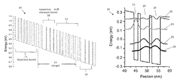
- FIG. 1 a is a conduction band diagram of a Quantum Cascade laser
- FIG. 1 b is an example of a ‘baseline’ design of a QCL quantum well emission layer
- FIG. 1 c is an example of a “lower efficiency” QCL active region with a scattering barrier disposed in the 2 nd quantum well;
- FIG. 1 d is an example of a “higher efficiency” QCL active region with a scattering barrier disposed in the 3 rd quantum well;
- FIG. 2 is a conduction band diagram of a QC laser with the parabolas representing the energy dispersion for upper (subband 2) and lower (subband 1) laser levels;
- FIG. 3 a is a graph showing upper laser level lifetimes calculated for different QC laser designs in various wavelength regions
- FIG. 3 b is a graph showing lower laser level lifetimes calculated for different QC laser designs in various wavelength regions
- FIG. 4 is a graph showing the calculated upper laser level lifetimes when both LO-phonon and IFR scattering are taken into account as a function of wavelength;
- FIG. 6 is a graph showing measured transit lifetimes as a function of the lasing wavelength.
- FIG. 7 is a graph showing the calculated upper laser level lifetimes plotted as a function of half the measured transit lifetimes with (triangles) and without (circles) taking into account of interface roughness scattering.
- Quantum Cascade (QC) lasers have become one of the key optical sources in the midinfrared (mid-IR) spectral range.
- QC lasers are well suited for applications in health and environmental sensing such as greenhouse gas monitoring and air pollutant detection, etc. For this reason, there is strong interest in the optimization of QC laser performance at room temperature with high power efficiency. Much effort has been undertaken in optimizing the QC laser performance over the years. Since QC lasers are semiconductor lasers based on intersubband transitions in quantum wells, one of the most important parameters in QC laser performance is the relationship between the lifetimes of the upper and lower laser subbands, which determines the magnitude of population inversion. Therefore, it is important to accurately account for intersubband scattering when designing QC lasers.
- the intersubband transition lifetimes can be determined by various scattering processes such as longitudinal optical (LO) phonons, longitudinal acoustic optical (LA) phonons, alloy disorder, or ionized impurities.
- LO longitudinal optical
- LA longitudinal acoustic optical
- impurities such as alloy disorder, or ionized impurities.
- interface roughness also causes intersubband scattering. Interface roughness induced scattering may have effects on the intersubband absorption, the temperature dependent intersubband broadening and the transport process limited by resonant tunneling, all of which strongly affect the QC laser performance.
- FIG. 1 a is a schematic conduction band diagram of a Quantum Cascade laser (QCL) 10 .
- the QCL 10 generally includes a plurality stages 12 configured in a cascade structure, each stage 12 having an injection layer 14 and a quantum well emission layer 16 . Each stage also has one or more upper laser levels and lower laser level(s). Light is generated by an intersubband transition of electrons from an upper laser level to a lower laser level in the quantum well emission layer as discussed in more detail below.
- FIG. 1 b is an example of a ‘baseline’ design (band structure) of a QCL quantum well emission layer (active region) 20 .
- the active region includes several quantum wells 21 , 23 , 25 .
- Several energy levels 22 , 24 , 26 and 28 are also illustrated. Of these energy levels, laser levels 24 and 26 actually participate in lasing transition as upper/lower laser levels. That is, light is generated via intersubband transition of electrons from upper laser level 24 to lower laser level 26 in the quantum well emission layer.
- FIG. 1 c is an example of a “lower efficiency” QCL active region 30 with a scattering barrier 37 disposed in the 2 nd quantum well 33 .
- the active region includes three quantum wells 31 , 33 , 35 .
- Several energy levels 32 , 34 , 36 and 38 are also illustrated. Of these energy levels, laser levels 34 and 36 actually participate in lasing transition as upper/lower laser levels.
- a scattering barrier should be located in a quantum well such that scattering for the lower laser level 36 is greater than scattering for the upper laser level 34 .
- the scattering barrier may be placed to maximize scattering for the lower laser level 36 and/or minimize scattering for the upper laser level 34 . In general scattering increases at peaks in the laser level.
- the scattering barrier 37 (monolayer) is located such that scattering for the lower laser level 36 is lower than scattering for the upper laser level 34 . That is, the scattering barrier 37 is placed in the 2nd quantum well where a peak in the wave function of the upper laser level 34 overlaps with the lower laser level 36 .
- theoretical calculations show about 50% reduction of upper state lifetime, which would in turn degrade the device performance over the baseline design shown in FIG. 1 b.
- FIG. 1 d is an example of a ‘higher efficiency’ QCL design 42 with a scattering barrier 47 in the 3rd quantum well 45 to speed up the carrier extraction from the lower laser state.
- the active region includes three quantum wells 41 , 43 , 45 .
- Several energy levels 42 , 44 , 46 and 48 are also illustrated. Of these energy levels, laser levels 44 and 46 actually participate in lasing transition as upper/lower laser levels.
- the scattering barrier 47 is located such that scattering the lower laser level 46 is greater than scattering for the upper laser level 44 . That is, the scattering barrier 47 is positioned such that the peak in the lower energy level 46 (as measured from the zero level for the lower energy level) is significantly higher than the peak in the upper laser level 44 (as measured from the zero level for the upper laser level). This would result in roughly an increase of 35% in gain, and ⁇ 50% higher slope efficiency compared to the base design in FIG. 1 b . As explained above, In order to maximize the performance increase the scattering barrier may be placed to maximize scattering for the lower laser level 46 and/or minimize scattering for the upper laser level 44 .
- FIG. 1 a Traditional QCL structures ( FIG. 1 a ) are typically designed using LO design criteria and are therefore dimensioned using LO-phonon spacing ( ⁇ 35-40 meV).
- the energy difference between the lower laser state and the state below may be much larger than one LO-phonon energy in order to minimize thermal back filling.
- Such QCL designs are well suited for high temperature laser applications.
- the scattering barriers 37 and 47 are generally configured with a minimal thickness 49 , e.g., ⁇ 0.30 nm, to preserve the geometry of an existing QCL design.
- the scattering barriers may be treated as one of the layers in QC laser structure, grown during the same growth process as the rest of the QC laser structure.
- the growing techniques may include typical deposition technique such as molecular beam epitaxy (MBE) and eetalorganic chemical vapor deposition (MOCVD). It should be understood that the thickness of the scattering barrier may be selected to alter the geometry and performance of a QCL design (to set laser parameters).
- MBE molecular beam epitaxy
- MOCVD eetalorganic chemical vapor deposition
- the quantum well emission layer may be configured with a plurality of quantum wells. Two or more quantum wells may be configured each with a scattering barrier positioned such that interface roughness (IFR) scattering at the lower laser level is greater than IFR scattering at the upper laser level.
- IFR interface roughness
- Interface roughness can be modeled as a random profile with Gaussian autocorrelation which is characterized by an average root-mean-square step height ⁇ and an in-plane correlation length ⁇ .
- the intersubband scattering lifetime ( ⁇ IFR ) caused by interface roughness can then be calculated:
- h _ ⁇ ⁇ IFR ⁇ ⁇ ⁇ m * h _ 2 ⁇ ⁇ 2 ⁇ ⁇ 2 ⁇ ⁇ ⁇ ⁇ U 2 ⁇ ⁇ i ⁇ ⁇ f 2 ⁇ ( z i ) ⁇ f 1 ⁇ ( z i ) ⁇ 2 ⁇ e - ⁇ 2 ⁇ q 21 2 4 ( 1 )
- ⁇ U is the band offset
- f 2 (z i ) and f 1 (z i ) are the wave function amplitudes at the ith interface
- q 21 is the absolute value of the two-dimensional scattering vector in this process. It should be understood that increasing the interface roughness may result in increased performance since the ⁇ term is squared in EQ. 1. Accordingly, the interface roughness may be modified or controlled during or after formation, e.g., using growth interrupts or other techniques.
- FIG. 2 shows the band structure of a QC laser with the parabolas representing the energy dispersion for upper (subband 2) and lower (subband 1) laser levels.
- the arrow q 21 illustrates the interface roughness induced transition from subband 2 to subband 1.
- a constant ⁇ ⁇ 0.15 nm which is about half of the monolayer thickness and a ⁇ ⁇ 6 nm are used for all the designs analyzed in the following interface roughness scattering calculations.
- FIG. 3 a is a graph showing upper laser level lifetimes calculated for different QC laser designs in various wavelength regions.
- FIG. 3 b is a graph showing lower laser level lifetimes calculated for different QC laser designs in various wavelength regions.
- Squares are lifetimes calculated by IFR scattering only.
- Circles are lifetimes calculated by LO phonon scattering only.
- Triangles are lifetimes taking into account of both IFR and LO phonon scattering.
- ⁇ IFR the lifetimes calculated from IFR scattering
- ⁇ LO LO-phonon scattering
- FIG. 4 is a graph showing the calculated upper laser level lifetimes when both LO-phonon and IFR scattering are taken into account as a function of wavelength.
- the dashed line is a guide for the eye only. Even though LO-phonon scattering still dominates at the shorter wavelength range ( ⁇ 4 ⁇ m), the calculated ⁇ total is reduced by almost 50% when including IFR scattering. Plotting the calculated ⁇ total as a function of lasing wavelength, the dependence of upper laser level lifetimes on the wavelength is clearly seen.
- the conventional depopulation energy for the lower laser level is designed to be around 34 meV for the QC laser designs we analyze here, so the difference between ⁇ IFR of the lower laser level has very little dependence on the depopulation energy.
- the material compositions for different wavelength range designs are different, thus affecting the band offset ⁇ U in Eq. (1).
- For QC lasers with design wavelength >8 ⁇ m lattice-matched In 0.53 Ga 0.47 As/Al 0.48 In 0.52 As on InP is used; for QC lasers with ⁇ 8 ⁇ m design wavelength, strain-balanced material is used to create a larger band offset.
- the larger band offset for short wavelength QC laser designs results in the domination of the lower laser level lifetime by IFR scattering as can be seen in FIG. 3 b.
- Quantum Cascade lasers are usually designed to have a sufficiently quick electron injection from the preceding injector to the upper laser level through resonant tunneling (see FIG. 2 ), and electrons depopulate similarly fast from the lower laser level to the following injector.
- the current density can be written as:
- the J max of a QC device is determined as shown in FIG. 5 .
- the inset in FIG. 5 shows the light-current-voltage characteristics of the laser fabricated from the same QC wafer.
- the cut-off voltage is the same for both the lasing and non-lasing QC devices though J max increases for a laser device due to the reduction of differential resistance when there is stimulated emission.
- J max for all 14 QC designs determined and using Ns of each design, ⁇ transit can be extracted.
- the measured ⁇ transit are plotted in FIG. 5 as a function of lasing wavelength.
- a similar dependence on the lasing wavelength for the measured ⁇ transit is also seen as in the case for the calculated ⁇ up ( FIG. 4 ).
- FIG. 7 is a graph showing the calculated upper laser level lifetimes plotted as a function of half the measured transit lifetimes with (triangles) and without (circles) taking into account of interface roughness scattering.
- the inset table lists the slopes, standard error and correlation coefficients of the fit curves.
- FIG. 7 the ⁇ up calculated using LO-phonon scattering only are plotted as circles, the line (linear fit) through all the data points has a slope of 0.43, standard error 0.27 and correlation coefficient of 0.43; the ⁇ up calculated with both LO-phonon and IFR scattering are plotted as triangles, the line (linear fit) through all the data points has a slope of 0.66, standard error 0.15 and correlation coefficient 0.79.
- the much smaller error and the larger correlation coefficient indicate a better agreement between the measured ⁇ transit and the calculated ⁇ up when IFR scattering is taken into account, which confirms that IFR scattering plays a non-negligible role for intersubband scattering in mid-IR QC lasers.
- FIG. 6 is a graph showing measured transit lifetimes as a function of the lasing wavelength. The different shapes indicate different growth facilities and growth techniques.
- the disclosed techniques position extra interfaces strategically into the conventional QCL design to facilitate carrier depopulation, and broaden the gain spectrum.
- the disclosed techniques also relax the traditional design criteria which can help improve device temperature performance.
- the traditional QCL structures designed using LO-phonon design criteria are typically dimensioned using optical phonon spacing ( ⁇ 35-40 meV). Designs based on the techniques herein may use a spacing between subsequent energy levels in excess of LO-phonon spacing.
- Resulting devices are well suited for applications such as trace gas sensing, breath analysis, glucose testing, etc., as well as IR countermeasures, and have advantages including being non-invasive, portable, and high power.
- Resulting devices may be made, e.g., from molecular beam epitaxy (MBE) or metalorganic chemical vapor deposition (MO CVD).
- MBE molecular beam epitaxy
- MO CVD metalorganic chemical vapor deposition
Landscapes
- Physics & Mathematics (AREA)
- Condensed Matter Physics & Semiconductors (AREA)
- General Physics & Mathematics (AREA)
- Electromagnetism (AREA)
- Optics & Photonics (AREA)
- Geometry (AREA)
- Semiconductor Lasers (AREA)
Abstract
Description
Claims (18)
Priority Applications (1)
| Application Number | Priority Date | Filing Date | Title |
|---|---|---|---|
| US13/624,330 US9054497B2 (en) | 2011-09-21 | 2012-09-21 | Quantum cascade lasers with improved performance using interface roughness scattering |
Applications Claiming Priority (2)
| Application Number | Priority Date | Filing Date | Title |
|---|---|---|---|
| US201161537409P | 2011-09-21 | 2011-09-21 | |
| US13/624,330 US9054497B2 (en) | 2011-09-21 | 2012-09-21 | Quantum cascade lasers with improved performance using interface roughness scattering |
Publications (2)
| Publication Number | Publication Date |
|---|---|
| US20150131689A1 US20150131689A1 (en) | 2015-05-14 |
| US9054497B2 true US9054497B2 (en) | 2015-06-09 |
Family
ID=53043787
Family Applications (1)
| Application Number | Title | Priority Date | Filing Date |
|---|---|---|---|
| US13/624,330 Expired - Fee Related US9054497B2 (en) | 2011-09-21 | 2012-09-21 | Quantum cascade lasers with improved performance using interface roughness scattering |
Country Status (1)
| Country | Link |
|---|---|
| US (1) | US9054497B2 (en) |
Families Citing this family (1)
| Publication number | Priority date | Publication date | Assignee | Title |
|---|---|---|---|---|
| JP7407546B2 (en) * | 2019-09-24 | 2024-01-04 | 株式会社東芝 | quantum cascade laser |
Citations (2)
| Publication number | Priority date | Publication date | Assignee | Title |
|---|---|---|---|---|
| US6829269B2 (en) * | 2002-05-21 | 2004-12-07 | University Of Massachusetts | Systems and methods using phonon mediated intersubband laser |
| US20100111127A1 (en) * | 2007-01-18 | 2010-05-06 | Hamamatsu Photonics K.K. | Quantum cascade laser |
-
2012
- 2012-09-21 US US13/624,330 patent/US9054497B2/en not_active Expired - Fee Related
Patent Citations (2)
| Publication number | Priority date | Publication date | Assignee | Title |
|---|---|---|---|---|
| US6829269B2 (en) * | 2002-05-21 | 2004-12-07 | University Of Massachusetts | Systems and methods using phonon mediated intersubband laser |
| US20100111127A1 (en) * | 2007-01-18 | 2010-05-06 | Hamamatsu Photonics K.K. | Quantum cascade laser |
Non-Patent Citations (22)
| Title |
|---|
| A. Bismuto, R. Terazzi, M. Beck, and J. Faist, "Influence of the growth temperature on the performances of strain-balanced quantum cascade lasers", Appl. Phys. Lett., 98, 091105 (2011). |
| A. Evans, S. R. Darvish, S. Slivken, J. Nguyen, Y. Bai, M. Razeghi, "Buried heterostructure quantum cascade lasers with high continuous-wave wall plug efficiency", Appl. Phys. Lett., 91, 071101 (2007). |
| C. Sirtori, F. Capasso, J. Faist, A. Hutchinson, D. Sivco, and A. Cho, "Resonant Tunneling in Quantum Cascade Lasers", IEEE J. Quantum Electron., 34, 1722 (1998). |
| J. B. Khurgin, "Inhomogeneous origin of the interface roughness broadening of intersubband transitions", Appl. Phys. Lett., 93, 091104 (2008). |
| J. B. Khurgin, Y. Dikmelik, "Transport and gain in a quantum cascade laser: model and equivalent circuit", Opt. Eng., 49(11),111110 (2010). |
| J. B. Khurgin, Y. Dikmelik, P. Q. Liu, A. J. Hoffman, M. D. Escarra, K. J. Franz, and C. F. Gmachl, "Role of interface roughness in the transport and lasing characteristics of quantum-cascade lasers", Appl. Phys. Lett., 94, 091101 (2009). |
| J. Faist, "Wallplug efficiency of quantum cascade lasers: Critical parameters and fundamental limits", Appl. Phys. Lett., 90, 253512 (2007). |
| J. Faist, F. Capasso, D. Sivco, C. Sirtori, A. Hutchinson, and A. Cho, "Quantum Cascade Laser", Science, 264, 553 (1994). |
| K. Fujita, M. Yamanishi, T. Edamura, A. Sugiyama, and S. Furuta, "Extremely high T0-values ( 450K) of long-wavelength ( 15mum), low-threshold-current-density quantum-cascade lasers based on the indirect pump scheme", Appl. Phys. Lett., 97, 201109 (2010). |
| K. Fujita, M. Yamanishi, T. Edamura, A. Sugiyama, and S. Furuta, "Extremely high T0-values ( 450K) of long-wavelength ( 15μm), low-threshold-current-density quantum-cascade lasers based on the indirect pump scheme", Appl. Phys. Lett., 97, 201109 (2010). |
| K. L. Campman, H. Schmidt, A. Imamoglu, and A. C. Gossard, "Interface roughness and alloydisorder scattering contributions to intersubband transition linewidths", Appl. Phys. Lett., 69, 2554 (1996). |
| M. P. Semtsiv, Y. Flores, M. Chashnikova, G. Monastyrskyi, and W. T. Masselink, "Low-threshold intersubband laser based on interface-scattering-rate engineering", Appl. Phys. Lett., 100, 163502 (2012). |
| P. Offermans, P. L. Koenraad, J. H. Wolter, M. Beck, T. Aellen, J. Faist, "Digital alloy interface grading of an InAlAs/InGaAs quantum cascade laser structure studied by cross-sectional scanning tunneling microscopy", Appl. Phys. Lett., 83, pp. 4131-4133 (2003). |
| P. Q. Liu, A. J. Hoffman, M. D. Escarra, K. J. Franz, J. B. Khurgin, Y. Dikmelik, X. Wang, J.Y. Fan, and C. F. Gmachl, "Highly power-efficient quantum cascade lasers", Nature Photonics, 4, 95-98 (2010). |
| R. Ferreira and G. Bastard, "Evaluation of some scattering times for electrons in unbiased and biased single- and multiple-quantum-well structures", Phys. Rev. B, 40, 1074 (1989). |
| T. Unuma, M. Yoshita, T. Noda, H. Sakaki, and H. Akiyama, J., "Intersubband absorption linewidth in GaAs quantum wells due to scattering by interface roughness, phonons. alloy disorder, and impurities", Appl. Phys., 93, 1586 (2003). |
| T. Unuma, T. Takahashi, T. Noda, M. Yoshita, H. Sakaki, M. Baba, and H. Akiyama, "Effects of interface roughness and phonon scattering on intersubband absorption linewidth in a GaAs quantum well", Appl. Phys. Lett., 78, 3448 (2001). |
| X. Huang, W. O. Charles, and C. F. Gmachl, "Temperature-insensitive long-wavelength Quantum Cascade lasers with low threshold", Opt. Express, 19, 8297-8302 (2011). |
| Y. Bai, S. Slivken, S. Kuboya, S. R. Darvish, and M. Razeghi, "Quantum cascade lasers that emit more light than heat", Nature Photonics, 4, 99-102 (2010). |
| Y. Yao, W. O. Charles, T. Tsai, J. Chen, G. Wysocki, and C. F. Gmachl, "Broadband quantum cascade laser gain medium based on a "continuum-to-bound" active region design", Appl. Phys. Lett., 96, 211106 (2010). |
| Y. Yao, X. Wang, J.Y. Fan, and C. F. Gmachl, "High performance "continuum-to-continuum" quantum cascade lasers with a broad gain bandwidth of over 400 cm-1", Appl. Phys. Lett., 97, 081115 (2010). |
| Z. Liu, D. Wasserman, S. S. Howard, A. J. Hoffman, C. F. Gmachl, X. Wang, T. Tanbun-Ek, L. Cheng, and F.S. Choa, "Room-Temperature Continuous-Wave Quantum Cascade Lasers Grown by MOCVD Without Lateral Regrowth", IEEE PTL., 18, 12, 1347-1349 (2006). |
Also Published As
| Publication number | Publication date |
|---|---|
| US20150131689A1 (en) | 2015-05-14 |
Similar Documents
| Publication | Publication Date | Title |
|---|---|---|
| Wienold et al. | Frequency dependence of the maximum operating temperature for quantum-cascade lasers up to 5.4 THz | |
| Chiu et al. | Importance of interface roughness induced intersubband scattering in mid-infrared quantum cascade lasers | |
| Aellen et al. | Doping in quantum cascade lasers. I. InAlAs–InGaAs∕ InP midinfrared devices | |
| US5978397A (en) | Article comprising an electric field-tunable semiconductor laser | |
| US7158545B2 (en) | Terahertz lasers and amplifiers based on resonant optical phonon scattering to achieve population inversion | |
| Alymov et al. | Fundamental limits to far-infrared lasing in Auger-suppressed HgCdTe quantum wells | |
| Ozaki et al. | Superluminescent diode with a broadband gain based on self-assembled InAs quantum dots and segmented contacts for an optical coherence tomography light source | |
| Ikonnikov et al. | Terahertz radiation generation in multilayer quantum-cascade heterostructures | |
| Yang et al. | Distributed feedback mid-IR interband cascade lasers at thermoelectric cooler temperatures | |
| Sandall et al. | Temperature dependence of threshold current in p-doped quantum dot lasers | |
| US9054497B2 (en) | Quantum cascade lasers with improved performance using interface roughness scattering | |
| Ulrich et al. | Temperature dependence of far-infrared electroluminescence in parabolic quantum wells | |
| Razeghi | High-power high-wall plug efficiency mid-infrared quantum cascade lasers based on InP/GaInAs/InAlAs material system | |
| Faist et al. | Terahertz quantum cascade lasers | |
| Cuscó et al. | Raman-scattering study of photoexcited plasma in semiconducting and semi-insulating InP | |
| Lim et al. | Simulation of double quantum well GaInNAs laser diodes | |
| Yang et al. | Dispersion of effective refractive indices of mid-infrared quantum cascade lasers | |
| Bismuto | Mid-infrared quantum cascade lasers: active medium and waveguide engineering | |
| Zhang et al. | Directional collimation of substrate emitting quantum cascade laser by nanopores arrays | |
| Flores | Mid-infrared quantum cascade lasers: theoretical and experimental studieson temperature-driven scattering | |
| Jacobs et al. | Photoluminescence Characterisation of High Current Density Resonant Tunnelling Diodes for Terahertz Applications | |
| Mann et al. | Influence of injector doping concentration on the performance of InP-based quantum-cascade lasers | |
| Bouzi | High performance quantum cascade lasers: Loss, beam stability, and gain engineering | |
| Eales | Influence of electronic band structure on the efficiency of mid-infrared photonic devices. | |
| Zhu | MBE growth, fabrication, and electrical characterisation of terahertz frequency quantum cascade lasers |
Legal Events
| Date | Code | Title | Description |
|---|---|---|---|
| AS | Assignment |
Owner name: THE JOHN HOPKINS UNIVERSITY, MARYLAND Free format text: ASSIGNMENT OF ASSIGNORS INTEREST;ASSIGNORS:DIKMELIK, YAMAC;KHURGIN, JACOB B;REEL/FRAME:032684/0946 Effective date: 20130718 Owner name: THE TRUSTEES OF PRINCETON UNIVERSITY, NEW JERSEY Free format text: ASSIGNMENT OF ASSIGNORS INTEREST;ASSIGNORS:GMACHL, CLAIRE;CHIU, YENTING;SIGNING DATES FROM 20140415 TO 20140416;REEL/FRAME:032684/0842 |
|
| STCF | Information on status: patent grant |
Free format text: PATENTED CASE |
|
| AS | Assignment |
Owner name: NATIONAL SCIENCE FOUNDATION, VIRGINIA Free format text: CONFIRMATORY LICENSE;ASSIGNOR:PRINCETON UNIVERSITY;REEL/FRAME:035905/0515 Effective date: 20150611 |
|
| CC | Certificate of correction | ||
| MAFP | Maintenance fee payment |
Free format text: PAYMENT OF MAINTENANCE FEE, 4TH YR, SMALL ENTITY (ORIGINAL EVENT CODE: M2551) Year of fee payment: 4 |
|
| FEPP | Fee payment procedure |
Free format text: MAINTENANCE FEE REMINDER MAILED (ORIGINAL EVENT CODE: REM.); ENTITY STATUS OF PATENT OWNER: SMALL ENTITY |
|
| LAPS | Lapse for failure to pay maintenance fees |
Free format text: PATENT EXPIRED FOR FAILURE TO PAY MAINTENANCE FEES (ORIGINAL EVENT CODE: EXP.); ENTITY STATUS OF PATENT OWNER: SMALL ENTITY |
|
| STCH | Information on status: patent discontinuation |
Free format text: PATENT EXPIRED DUE TO NONPAYMENT OF MAINTENANCE FEES UNDER 37 CFR 1.362 |
|
| FP | Lapsed due to failure to pay maintenance fee |
Effective date: 20230609 |