US9054157B2 - High performance on-chip vertical coaxial cable, method of manufacture and design structure - Google Patents
High performance on-chip vertical coaxial cable, method of manufacture and design structure Download PDFInfo
- Publication number
- US9054157B2 US9054157B2 US14/076,656 US201314076656A US9054157B2 US 9054157 B2 US9054157 B2 US 9054157B2 US 201314076656 A US201314076656 A US 201314076656A US 9054157 B2 US9054157 B2 US 9054157B2
- Authority
- US
- United States
- Prior art keywords
- coaxial cable
- conductor
- design
- shape
- inner conductor
- Prior art date
- Legal status (The legal status is an assumption and is not a legal conclusion. Google has not performed a legal analysis and makes no representation as to the accuracy of the status listed.)
- Active
Links
Images


Classifications
-
- H—ELECTRICITY
- H01—ELECTRIC ELEMENTS
- H01L—SEMICONDUCTOR DEVICES NOT COVERED BY CLASS H10
- H01L21/00—Processes or apparatus adapted for the manufacture or treatment of semiconductor or solid state devices or of parts thereof
- H01L21/70—Manufacture or treatment of devices consisting of a plurality of solid state components formed in or on a common substrate or of parts thereof; Manufacture of integrated circuit devices or of parts thereof
- H01L21/71—Manufacture of specific parts of devices defined in group H01L21/70
- H01L21/768—Applying interconnections to be used for carrying current between separate components within a device comprising conductors and dielectrics
-
- G06F17/505—
-
- G—PHYSICS
- G06—COMPUTING; CALCULATING OR COUNTING
- G06F—ELECTRIC DIGITAL DATA PROCESSING
- G06F30/00—Computer-aided design [CAD]
- G06F30/30—Circuit design
- G06F30/32—Circuit design at the digital level
- G06F30/327—Logic synthesis; Behaviour synthesis, e.g. mapping logic, HDL to netlist, high-level language to RTL or netlist
-
- H—ELECTRICITY
- H01—ELECTRIC ELEMENTS
- H01L—SEMICONDUCTOR DEVICES NOT COVERED BY CLASS H10
- H01L23/00—Details of semiconductor or other solid state devices
- H01L23/48—Arrangements for conducting electric current to or from the solid state body in operation, e.g. leads, terminal arrangements ; Selection of materials therefor
- H01L23/488—Arrangements for conducting electric current to or from the solid state body in operation, e.g. leads, terminal arrangements ; Selection of materials therefor consisting of soldered or bonded constructions
- H01L23/498—Leads, i.e. metallisations or lead-frames on insulating substrates, e.g. chip carriers
- H01L23/49827—Via connections through the substrates, e.g. pins going through the substrate, coaxial cables
-
- H—ELECTRICITY
- H01—ELECTRIC ELEMENTS
- H01L—SEMICONDUCTOR DEVICES NOT COVERED BY CLASS H10
- H01L23/00—Details of semiconductor or other solid state devices
- H01L23/52—Arrangements for conducting electric current within the device in operation from one component to another, i.e. interconnections, e.g. wires, lead frames
- H01L23/522—Arrangements for conducting electric current within the device in operation from one component to another, i.e. interconnections, e.g. wires, lead frames including external interconnections consisting of a multilayer structure of conductive and insulating layers inseparably formed on the semiconductor body
- H01L23/5222—Capacitive arrangements or effects of, or between wiring layers
- H01L23/5225—Shielding layers formed together with wiring layers
-
- H—ELECTRICITY
- H01—ELECTRIC ELEMENTS
- H01L—SEMICONDUCTOR DEVICES NOT COVERED BY CLASS H10
- H01L23/00—Details of semiconductor or other solid state devices
- H01L23/52—Arrangements for conducting electric current within the device in operation from one component to another, i.e. interconnections, e.g. wires, lead frames
- H01L23/522—Arrangements for conducting electric current within the device in operation from one component to another, i.e. interconnections, e.g. wires, lead frames including external interconnections consisting of a multilayer structure of conductive and insulating layers inseparably formed on the semiconductor body
- H01L23/5226—Via connections in a multilevel interconnection structure
-
- H—ELECTRICITY
- H01—ELECTRIC ELEMENTS
- H01L—SEMICONDUCTOR DEVICES NOT COVERED BY CLASS H10
- H01L2924/00—Indexing scheme for arrangements or methods for connecting or disconnecting semiconductor or solid-state bodies as covered by H01L24/00
-
- H—ELECTRICITY
- H01—ELECTRIC ELEMENTS
- H01L—SEMICONDUCTOR DEVICES NOT COVERED BY CLASS H10
- H01L2924/00—Indexing scheme for arrangements or methods for connecting or disconnecting semiconductor or solid-state bodies as covered by H01L24/00
- H01L2924/0001—Technical content checked by a classifier
- H01L2924/0002—Not covered by any one of groups H01L24/00, H01L24/00 and H01L2224/00
-
- Y—GENERAL TAGGING OF NEW TECHNOLOGICAL DEVELOPMENTS; GENERAL TAGGING OF CROSS-SECTIONAL TECHNOLOGIES SPANNING OVER SEVERAL SECTIONS OF THE IPC; TECHNICAL SUBJECTS COVERED BY FORMER USPC CROSS-REFERENCE ART COLLECTIONS [XRACs] AND DIGESTS
- Y10—TECHNICAL SUBJECTS COVERED BY FORMER USPC
- Y10T—TECHNICAL SUBJECTS COVERED BY FORMER US CLASSIFICATION
- Y10T29/00—Metal working
- Y10T29/49—Method of mechanical manufacture
- Y10T29/49002—Electrical device making
- Y10T29/49117—Conductor or circuit manufacturing
- Y10T29/49123—Co-axial cable
Definitions
- the present invention relates to the field of coaxial cables, and more particularly, to a high performance on-chip vertical coaxial cable, method of manufacturing the same and design structure thereof.
- a coaxial cable is an electrical cable generally applied as a high-frequency transmission line to carry a high frequency or broadband signal.
- the coaxial cable can be used for connecting radio transmitters and receivers with their antennas, Internet connections, and for distributing cable television signals, among other applications.
- DC power (called a bias) is added to the signal to supply the equipment at the other end, as in direct broadcast satellite receivers, with operating power.
- One advantage of the coaxial cable over other types of transmission line is that ideally the electromagnetic field carrying the signal exists only in the space between the inner and outer conductors, so the coaxial cable cannot interfere with or suffer interference from external electromagnetic fields.
- Another area which could utilize coaxial cables is integrated circuit technology. On-chip coaxial cable is advantageous in connecting integrated circuits to reduce the noise and crosstalk.
- Conventional on-chip coaxial cable is built within metal layers of a semiconductor chip and is typically arranged along a horizontal plane, as shown in FIG. 1 .
- this design has several disadvantages associated with it.
- One disadvantage involves the distance between an outside shielding conductor and a signal line. More specifically, in a conventional on-chip coaxial cable structure, since this structure is typically formed within metal layers and positioned along a horizontal plane, the distance between the outside conductor and the signal line is not substantially uniform and is limited by the available metal technologies in the semiconductor chip. Additionally, this prior art design limits the shape of the coaxial cable structure to a rectangular prism or a cube.
- a coaxial cable structure comprises an inner conductor and an insulating material that coaxially surrounds the inner conductor.
- the structure further comprises an outer conductor which surrounds the insulating material.
- Both the inner and outer conductors are comprised of a plurality of metal layers formed on different wiring levels and interconnected between the different wiring levels by conductors.
- the coaxial cable structure is formed upon a surface of a semiconductor substrate and is oriented in substantially perpendicular alignment with the surface.
- a method for fabricating a coaxial cable structure comprises forming a first shape of an inner conductor in a plurality of metal layers formed on different wiring levels and interconnected between the different wiring levels by a first conductor and forming a second shape of an outer conductor in the plurality of metal layers formed on different wiring levels and interconnected between the different wiring levels by a second conductor.
- the coaxial cable structure is formed upon a surface of a semiconductor substrate and is oriented in substantially perpendicular alignment with the surface.
- a design structure embodied in a machine readable medium for designing, manufacturing, or testing an integrated circuit.
- the design structure comprises the structures and/or methods of the present invention.
- FIG. 1 illustrates a perspective view of a coaxial wire in a semiconductor chip according to the prior art
- FIG. 2 illustrates a perspective view of a structure of cylindrically shaped vertical coaxial cable according to an embodiment of the present invention
- FIG. 3 illustrates a section view of the side of the cylindrically shaped vertical coaxial cable structure of FIG. 2 ;
- FIG. 4 illustrates a top view of the cylindrically shaped vertical coaxial cable structure of FIG. 2 ;
- FIG. 5A illustrates a perspective view of a structure of a vertical coaxial cable shaped as a hexagonal prism according to an embodiment of the present invention
- FIG. 5B illustrates a section view of the side of the vertical coaxial cable structure shaped as a hexagonal prism of FIG. 5A ;
- FIG. 5C illustrates a top view of the vertical coaxial cable structure shaped as a hexagonal prism of FIG. 5A ;
- FIG. 6A illustrates a perspective view of a structure of a vertical coaxial cable shaped as a uniform prism according to an embodiment of the present invention
- FIG. 6B illustrates a section view of the side of the vertical coaxial cable structure shaped as a uniform prism of FIG. 6A ;
- FIG. 6C illustrates a top view of the vertical coaxial cable structure shaped as a uniform prism of FIG. 6A ;
- FIG. 7 shows a graph of insertion loss versus frequency comparing different shapes of a vertical coaxial cable structure
- FIG. 8 is a graph that shows relationships between the dimensions of the inner and outer conductors and the characteristic impedance
- FIG. 9A illustrates a side view of one exemplary application of on-chip vertical coaxial cable structures according to an embodiment of the present invention.
- FIG. 9B illustrates a top view of one exemplary application of on-chip vertical coaxial cable structures of FIG. 9A ;
- FIG. 10 is a flow diagram of a design process used in semiconductor design, manufacture, and/or test.
- the present invention relates to the field of coaxial cables, and more particularly, to a high performance on-chip vertical coaxial cable, method of manufacturing the same and design structure thereof. More specifically, the present invention comprises an on-chip vertical coaxial cable structure having an inner conductor and an insulating material that coaxially surrounds the inner conductor. The structure further comprises an outer conductor which surrounds the insulating material. Both the inner and outer conductors are comprised of a plurality of metal layers formed on different wiring levels using back-end-of-line (BEOL) technology and interconnected between the different wiring levels by conductors.
- BEOL back-end-of-line
- the high performance on-chip vertical coaxial cable can be built with desirable characteristic impedance, while having, in a preferred embodiment, increased Radio Frequency (RF) performance compared with prior art conventional on-chip horizontal coaxial cable.
- RF Radio Frequency
- the structure of the present invention includes multiple metal layers formed above the semiconductor portion of the substrate using BEOL technology.
- metal lines run parallel to the substrate and conductive vias run perpendicular to the substrate, the conductive vias interconnecting the different levels of metal wiring lines.
- the structure of the present invention is an improvement over prior art as it is oriented in substantially perpendicular alignment with the semiconductor portion of the substrate 902 (as shown in FIG. 9A ). This advantageous alignment will provide enhanced design flexibility for high performance on-chip coaxial cable.
- FIG. 1 illustrates a perspective view of a horizontal coaxial wire in a semiconductor chip according to the prior art. Shown in FIG. 1 are metal layers 102 , 104 and 106 , dielectric layers 108 and 110 , a signal wire 112 , side shield wires 118 and 120 , and vias 122 , 124 , 126 and 128 .
- the vertical shield wires 118 and 120 are formed as wide traces according to well known techniques.
- the vertical shield wires 118 and 120 typically have same length as the signal wire 112 .
- the side shield wires 114 and 116 are formed on opposite sides of the signal wire 112 according to well known techniques.
- the vertical shield wires 118 and 120 typically have a trace width that extends to the outside of the side shield wires 114 and 116 .
- the vias 122 , 124 , 126 and 128 are formed in the dielectric layers 108 and 110 , in the same manner used for making vias in a typical semiconductor die.
- the length and width of the vias 122 , 124 , 126 and 128 are typically equal to the corresponding dimensions of the side shield wires 114 and 116 .
- the vias 122 , 124 , 126 and 128 electrically connect the side shield wires 114 and 116 to the vertical shield wires 118 and 120 as shown in FIG.
- the conventional design imposes, among other things, significant geometrical limitations.
- the distance between the vertical shield wires 118 and 120 and a signal wire 112 is limited by an available BEOL technology.
- the geometrical shape of the conventional horizontal coaxial wire is limited to a rectangular prism or cube. The present invention, however, contemplates that the shapes and dimensions of both the inner and outer conductors may vary to achieve the desired level of characteristic impedance and to improve the RF performance.
- FIG. 2 illustrates a perspective view of a structure of cylindrically shaped vertical coaxial cable in accordance with aspects of the invention.
- the structure of the vertical coaxial cable includes an inner conductor 206 and an outer conductor 202 .
- the inner conductor 206 comprises a signal line.
- the inner conductor 206 is utilized to transmit RF signals.
- the outer conductor 202 comprises a shielding layer or a ground line.
- the electromagnetic field carrying the signal exists (ideally) only in the space between the inner conductor and outer conductor, so the coaxial cable cannot interfere with or suffer interference from external electromagnetic fields.
- the structure of the outer conductor includes multiple metal layers formed above the semiconductor portion of the substrate using damascene processes conventionally associated with BEOL technology.
- the plurality of metal layers 210 are arranged in parallel above the semiconductor portion of the substrate.
- each metal layer 210 has circular shape.
- the outer conductor structure 202 is shown with four metal layers 210 ; however, the number of metal layers can depend on type of the BEOL technology utilized and can be scaled for newer technologies.
- metal layers 210 , 510 , 610 can be made from any metal conductor.
- Advantageous metals for this purpose are aluminum (Al) or copper (Cu).
- the structure of the outer conductor 202 also includes multiple dielectric layers 208 between each of the metal layers 210 , as shown in FIGS. 2 and 3 .
- Dielectric layers 208 may comprise any organic or inorganic material recognized by a person having ordinary skill in the art, which may be deposited by any number of well known conventional techniques such as sputtering, spin-on application, chemical vapor deposition (CVD) process or a plasma enhanced CVD (PECVD) process.
- CVD chemical vapor deposition
- PECVD plasma enhanced CVD
- Candidate inorganic dielectric materials for dielectric layers 208 may include, but are not limited to, silicon dioxide, fluorine-doped silicon glass (FSG), and combinations of these dielectric materials.
- dielectric material constituting dielectric layers 208 may be characterized by a relative permittivity or dielectric constant smaller than the dielectric constant of silicon dioxide, which is about 3.9.
- dielectric constant of silicon dioxide which is about 3.9.
- dielectric layers 208 include, but are not limited to, porous and nonporous spin-on organic low-k dielectrics, such as spin-on aromatic thermoset polymer resins, porous and non-porous inorganic low-k dielectrics, such as organosilicate glasses, hydrogen-enriched silicon oxycarbide (SiCOH), and carbon-doped oxides, and combinations of organic and inorganic dielectrics.
- dielectric layers 208 also have circular geometry.
- metal layers 210 are interconnected by rows of spaced-apart vias 212 defined in dielectric layers 208 .
- Vias are usually formed as holes in a dielectric layer that are filled with an electrically conductive metal, for example, the same material used in metal layers 210 .
- the vias 212 which extend vertically in dielectric levels 208 of the BEOL structure, electrically connect adjacent metal layers 210 .
- inner conductor 206 has a structure (not shown) substantially similar to the previously described structure of outer conductor 202 .
- inner conductor 206 has the same shape as outer conductor 202 in order to keep the same level of characteristic impedance.
- FIG. 4 illustrates a top view of the structure of cylindrically shaped vertical coaxial cable of FIG. 2 .
- the structure of the vertical coaxial cable is oriented in substantially perpendicular alignment with the semiconductor portion of the substrate 902 (as shown in FIG. 9A ).
- the insulating material 204 coaxially surrounds inner conductor 206 .
- Insulating material 204 is needed to maintain the spacing between inner conductor 206 and outer conductor 202 .
- outer conductor 202 coaxially surrounds insulating material 204 .
- Insulating material 204 may comprise any organic or inorganic dielectric material recognized by a person having ordinary skill in the art.
- Fabrication of insulating material layer 204 in a BEOL structure may involve, for example, but not limited to, patterning of metal layers 212 using lithography and metal reactive ion etch (RIE) techniques.
- RIE metal reactive ion etch
- insulating material 204 may be air.
- FIG. 5A illustrates a perspective view of an alternative structure of vertical coaxial cable according to another embodiment of the present invention.
- vertical coaxial cable is shaped as a hexagonal prism.
- the structure of the vertical coaxial cable is substantially the same as that previously described in conjunction with FIGS. 2-4 .
- the structure of the vertical coaxial cable includes an inner conductor 506 and an outer conductor 502 .
- parallel metal layers 510 and parallel dielectric layers 508 are shaped as regular hexagons. It must be noted that the structure of the vertical coaxial cable is oriented in substantially perpendicular alignment with the semiconductor portion of the substrate 902 (as shown in FIG. 9A ).
- FIGS. 5B and 5C illustrate a section view of the side and a top view of the vertical coaxial cable structure, respectively.
- metal layers 510 are interconnected by rows of spaced-apart vias 512 defined in dielectric layers 508 .
- vias 512 extend vertically along each side of hexagonally shaped metal layers 510 .
- FIG. 5C shows that insulating material 504 coaxially surrounds inner conductor 506 and is similarly shaped as a hexagon.
- FIG. 6A illustrates a perspective view of a structure of vertical coaxial cable according to yet another embodiment of the present invention.
- vertical coaxial cable is shaped as a substantially uniform prism.
- the structure of the vertical coaxial cable is substantially the same as that previously described in conjunction with FIGS. 2-4 .
- the structure of the vertical coaxial cable includes an inner conductor 606 and an outer conductor 602 .
- parallel metal layers 610 and parallel dielectric layers 608 are shaped as squares. It must be noted that the structure of the vertical coaxial cable is oriented in substantially perpendicular alignment with the semiconductor portion of the substrate 902 (as shown in FIG. 9A ).
- FIGS. 6B and 6C illustrate a section view of the side and a top view of the vertical coaxial cable structure, respectively.
- metal layers 610 are interconnected by rows of spaced-apart vias 612 defined in dielectric layers 608 .
- vias 612 extend vertically along each side of metal layers 610 shaped as squares.
- FIG. 6C shows that insulating material 604 coaxially surrounds inner conductor 606 and is similarly shaped as a square.
- FIG. 7 shows a graph of insertion loss versus frequency comparing different shapes of the vertical coaxial cable structure in accordance with aspects of the invention.
- the essential function of coaxial cables is to transmit high frequency energy and signals with low loss. Insertion loss is a common measurement that is used to determine the loss of signal power resulting from the interference from external electromagnetic fields.
- the cylindrically shaped vertical coaxial cable shows 702 a factor of at least two (2) decrease in insertion loss at frequency over 60 GHz, compared to other geometric shapes of the coaxial wire, such as hexagonal prism 704 and substantially uniform prism 706 .
- This graph demonstrates that changing a shape of the coaxial cable according to aspects of the present invention will result in improved RF performance relative to the prior art.
- FIG. 8 is a graph that shows relationships between the dimensions of the inner and outer conductors and the characteristic impedance.
- FIG. 8 demonstrates that changing a radius of inner conductor 206 of cylindrically shaped vertical coaxial cable structure shown, for example, in FIG. 2 , while keeping a radius of outer conductor 202 constant has substantial effect on the characteristic impedance of coaxial cable. For example, as shown in FIG. 8 , changing a radius of inner conductor 206 from 3 micron 806 to 1 micron 802 shows a factor of approximately 1.8 improvement of characteristic impedance. Similarly, changing a radius of inner conductor 206 from 5 micron 808 to 2 micron 804 shows a factor of approximately 1.85 improvement of characteristic impedance. In this exemplary embodiment, the radius of outer conductor 202 remains constant (7 microns).
- the characteristic impedance can be controlled by varying the length of each side of inner conductor 606 .
- the characteristic impedance may be controlled by changing dimensions of outer conductor 202 , 502 , 602 instead.
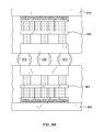
- FIG. 9A illustrates one exemplary application of high-performance on-chip vertical coaxial cable in accordance with embodiments of the present invention.
- vertical coaxial cables can be used as an inter-substrate connection.
- first vertical coaxial cable structure 904 (previously described in conjunction with FIGS. 2-6C ) is connected to a chip (not shown) and positioned perpendicular to the top surface of lower semiconductor substrate 902 .
- Second vertical coaxial cable structure 906 is positioned in a minor image orientation relative to first vertical coaxial cable structure 904 .
- Second vertical coaxial cable 906 is positioned perpendicular to the lower surface of upper semiconductor substrate 910 .
- Outer conductor 952 of first vertical coaxial cable 904 is joined with outer conductor (not shown) of second vertical coaxial cable 906 by solder balls 912
- inner conductor 954 of first vertical coaxial cable 904 is joined with inner conductor (not shown) of second vertical coaxial cable 906 by solder balls 912 , as seen in FIG. 9B .
- the exemplary interconnection structure illustrated in FIG. 9A allows high frequency inter-substrate signal transmission via respective inner conductors 954 .
- Embodiments of the present invention contemplate that on-chip vertical coaxial cable structure described herein can be used for, for example, but not limited to, connections with through silicon vias (TSVs) and various vertical components of integrated circuits.
- TSVs through silicon vias
- the present invention comprises an on-chip vertical coaxial cable structure having an inner conductor and an outer conductor that coaxially surrounds the inner conductor.
- Those conductors comprising a plurality of metal layers and interconnected by a plurality of vias, are formed using back-end-of-the-line (BEOL) technology.
- BEOL back-end-of-the-line
- the structures of the present invention could have any desirable shape.
- the high performance on-chip vertical coaxial cable can be built with a desired characteristic impedance, while having better RF performance compared with prior art conventional on-chip horizontal coaxial cable.
- FIG. 10 shows a block diagram of an exemplary design flow 1000 used for example, in semiconductor IC logic design, simulation, test, layout, and manufacture.
- Design flow 1000 includes processes, machines and/or mechanisms for processing design structures or devices to generate logically or otherwise functionally equivalent representations of the design structures and/or devices described above and shown in FIGS. 2-6C .
- the design structures processed and/or generated by design flow 1000 may be encoded on machine-readable transmission or storage media to include data and/or instructions that when executed or otherwise processed on a data processing system generate a logically, structurally, mechanically, or otherwise functionally equivalent representation of hardware components, circuits, devices, or systems.
- Machines include, but are not limited to, any machine used in an IC design process, such as designing, manufacturing, or simulating a circuit, component, device, or system.
- machines may include: lithography machines, machines and/or equipment for generating masks (e.g. e-beam writers), computers or equipment for simulating design structures, any apparatus used in the manufacturing or test process, or any machines for programming functionally equivalent representations of the design structures into any medium (e.g. a machine for programming a programmable gate array).
- Design flow 1000 may vary depending on the type of representation being designed. For example, a design flow 1000 for building an application specific IC (ASIC) may differ from a design flow 1000 for designing a standard component or from a design flow 1000 for instantiating the design into a programmable array, for example a programmable gate array (PGA) or a field programmable gate array (FPGA) offered by Altera® Inc. or Xilinx® Inc.
- ASIC application specific IC
- PGA programmable gate array
- FPGA field programmable gate array
- FIG. 10 illustrates multiple such design structures including an input design structure 1020 that is preferably processed by a design process 1010 .
- Design structure 1020 may be a logical simulation design structure generated and processed by design process 1010 to produce a logically equivalent functional representation of a hardware device.
- Design structure 1020 may also or alternatively comprise data and/or program instructions that when processed by design process 1010 , generate a functional representation of the physical structure of a hardware device. Whether representing functional and/or structural design features, design structure 1020 may be generated using electronic computer-aided design (ECAD) such as implemented by a core developer/designer.
- ECAD electronic computer-aided design
- design structure 1020 When encoded on a machine-readable data transmission, gate array, or storage medium, design structure 1020 may be accessed and processed by one or more hardware and/or software modules within design process 1010 to simulate or otherwise functionally represent an electronic component, circuit, electronic or logic module, apparatus, device, or system such as those shown in FIGS. 2-6C .
- design structure 1020 may comprise files or other data structures including human and/or machine-readable source code, compiled structures, and computer-executable code structures that when processed by a design or simulation data processing system, functionally simulate or otherwise represent circuits or other levels of hardware logic design.
- Such data structures may include hardware-description language (HDL) design entities or other data structures conforming to and/or compatible with lower-level HDL design languages such as Verilog and VHDL, and/or higher level design languages such as C or C++.
- HDL hardware-description language
- Design process 1010 preferably employs and incorporates hardware and/or software modules for synthesizing, translating, or otherwise processing a design/simulation functional equivalent of the components, circuits, devices, or logic structures shown in FIGS. 2-6C to generate a netlist 1080 which may contain design structures such as design structure 1020 .
- Netlist 1080 may comprise, for example, compiled or otherwise processed data structures representing a list of wires, discrete components, logic gates, control circuits, I/O devices, models, etc. that describes the connections to other elements and circuits in an integrated circuit design.
- Netlist 1080 may be synthesized using an iterative process in which netlist 1080 is resynthesized one or more times depending on design specifications and parameters for the device.
- netlist 1080 may be recorded on a machine-readable data storage medium or programmed into a programmable gate array.
- the medium may be a non-volatile storage medium such as a magnetic or optical disk drive, a programmable gate array, a compact flash, or other flash memory. Additionally, or in the alternative, the medium may be a system or cache memory, buffer space, or electrically or optically conductive devices and materials on which data packets may be transmitted and intermediately stored via the Internet, or other networking suitable means.
- Design process 1010 may include hardware and software modules for processing a variety of input data structure types including netlist 1080 .
- data structure types may reside, for example, within library elements 1030 and include a set of commonly used elements, circuits, and devices, including models, layouts, and symbolic representations, for a given manufacturing technology (e.g., different technology nodes, 32 nm, 45 nm, 90 nm, etc.).
- the data structure types may further include design specifications 1040 , characterization data 1050 , verification data 1060 , design rules 1070 , and test data files 1085 which may include input test patterns, output test results, and other testing information.
- Design process 1010 may further include, for example, standard mechanical design processes such as stress analysis, thermal analysis, mechanical event simulation, process simulation for operations such as casting, molding, and die press forming, etc.
- standard mechanical design processes such as stress analysis, thermal analysis, mechanical event simulation, process simulation for operations such as casting, molding, and die press forming, etc.
- One of ordinary skill in the art of mechanical design can appreciate the extent of possible mechanical design tools and applications used in design process 1010 without deviating from the scope and spirit of the invention.
- Design process 1010 may also include modules for performing standard circuit design processes such as timing analysis, verification, design rule checking, place and route operations, etc.
- Design process 1010 employs and incorporates logic and physical design tools such as HDL compilers and simulation model build tools to process design structure 1020 together with some or all of the depicted supporting data structures along with any additional mechanical design or data (if applicable), to generate a second design structure 1090 .
- Design structure 1090 resides on a storage medium or programmable gate array in a data format used for the exchange of data of mechanical devices and structures (e.g. information stored in an IGES, DXF, Parasolid XT, JT, DRG, or any other suitable format for storing or rendering such mechanical design structures).
- design structure 1090 preferably comprises one or more files, data structures, or other computer-encoded data or instructions that reside on transmission or data storage media and that when processed by an ECAD system generate a logically or otherwise functionally equivalent form of one or more of the embodiments of the invention shown in FIGS. 2-6C .
- design structure 1090 may comprise a compiled, executable HDL simulation model that functionally simulates the devices shown in FIGS. 2-6C .
- Design structure 1090 may also employ a data format used for the exchange of layout data of integrated circuits and/or symbolic data format (e.g. information stored in a GDSII (GDS2), GL1, OASIS, map files, or any other suitable format for storing such design data structures).
- Design structure 1090 may comprise information such as, for example, symbolic data, map files, test data files, design content files, manufacturing data, layout parameters, wires, levels of metal, vias, shapes, data for routing through the manufacturing line, and any other data required by a manufacturer or other designer/developer to produce a device or structure as described above and shown in FIGS. 2-6C .
- Design structure 1090 may then proceed to a stage 1095 where, for example, design structure 1090 proceeds to tape-out, is released to manufacturing, is released to a mask house, is sent to another design house, is sent back to the customer, etc.
Abstract
Description
Z 0=({acute over (η)}/2π)ln(D/d).
Claims (13)
Priority Applications (1)
| Application Number | Priority Date | Filing Date | Title |
|---|---|---|---|
| US14/076,656 US9054157B2 (en) | 2011-02-01 | 2013-11-11 | High performance on-chip vertical coaxial cable, method of manufacture and design structure |
Applications Claiming Priority (2)
| Application Number | Priority Date | Filing Date | Title |
|---|---|---|---|
| US13/018,963 US8629536B2 (en) | 2011-02-01 | 2011-02-01 | High performance on-chip vertical coaxial cable, method of manufacture and design structure |
| US14/076,656 US9054157B2 (en) | 2011-02-01 | 2013-11-11 | High performance on-chip vertical coaxial cable, method of manufacture and design structure |
Related Parent Applications (1)
| Application Number | Title | Priority Date | Filing Date |
|---|---|---|---|
| US13/018,963 Division US8629536B2 (en) | 2011-02-01 | 2011-02-01 | High performance on-chip vertical coaxial cable, method of manufacture and design structure |
Publications (2)
| Publication Number | Publication Date |
|---|---|
| US20140065817A1 US20140065817A1 (en) | 2014-03-06 |
| US9054157B2 true US9054157B2 (en) | 2015-06-09 |
Family
ID=46576406
Family Applications (2)
| Application Number | Title | Priority Date | Filing Date |
|---|---|---|---|
| US13/018,963 Expired - Fee Related US8629536B2 (en) | 2011-02-01 | 2011-02-01 | High performance on-chip vertical coaxial cable, method of manufacture and design structure |
| US14/076,656 Active US9054157B2 (en) | 2011-02-01 | 2013-11-11 | High performance on-chip vertical coaxial cable, method of manufacture and design structure |
Family Applications Before (1)
| Application Number | Title | Priority Date | Filing Date |
|---|---|---|---|
| US13/018,963 Expired - Fee Related US8629536B2 (en) | 2011-02-01 | 2011-02-01 | High performance on-chip vertical coaxial cable, method of manufacture and design structure |
Country Status (1)
| Country | Link |
|---|---|
| US (2) | US8629536B2 (en) |
Families Citing this family (3)
| Publication number | Priority date | Publication date | Assignee | Title |
|---|---|---|---|---|
| JP6344197B2 (en) * | 2014-10-30 | 2018-06-20 | 富士電機株式会社 | Semiconductor device |
| CN105226360B (en) * | 2015-08-24 | 2018-05-29 | 上海交通大学 | Substrate integrated coaxial waveguide interconnection array structure |
| US10070525B2 (en) * | 2016-12-28 | 2018-09-04 | Intel Corporation | Internal to internal coaxial via transition structures in package substrates |
Citations (16)
| Publication number | Priority date | Publication date | Assignee | Title |
|---|---|---|---|---|
| US5117276A (en) | 1989-08-14 | 1992-05-26 | Fairchild Camera And Instrument Corp. | High performance interconnect system for an integrated circuit |
| US5338897A (en) | 1991-07-30 | 1994-08-16 | Texas Instruments, Incorporated | Coaxial shield for a semiconductor device |
| US5357138A (en) | 1991-02-22 | 1994-10-18 | Nec Corporation | Coaxial wiring pattern structure in a multilayered wiring board |
| US5587119A (en) | 1994-09-14 | 1996-12-24 | E-Systems, Inc. | Method for manufacturing a coaxial interconnect |
| US20020139579A1 (en) | 2001-03-16 | 2002-10-03 | Bongsin Kwark | Electrical interconnect having a multi-layer circuit board structure and including a conductive spacer for impedance matching |
| US20030137053A1 (en) * | 2002-01-10 | 2003-07-24 | Sanyo Electric Co., Ltd. | Wiring structure and manufacturing method therefor, semiconductor device including wiring structure and wiring board |
| US6624521B2 (en) | 2001-07-20 | 2003-09-23 | Georgia Tech Research Corp. | Flip chip design on a coplanar waveguide with a pseudo-coaxial ground bump configuration |
| US6943452B2 (en) | 1999-03-09 | 2005-09-13 | International Business Machines Corporation | Coaxial wiring within SOI semiconductor, PCB to system for high speed operation and signal quality |
| US7015569B1 (en) | 2004-08-26 | 2006-03-21 | Lsi Logic Corporation | Method and apparatus for implementing a co-axial wire in a semiconductor chip |
| US20080093112A1 (en) | 2004-07-23 | 2008-04-24 | Taras Kushta | Composite Via Structures and Filters in Multilayer Printed Circuit Boards |
| US20090108465A1 (en) | 2006-12-13 | 2009-04-30 | International Business Machines Corporation | Ceramic substrate grid structure for the creation of virtual coax arrangement |
| US20090108457A1 (en) | 2007-10-31 | 2009-04-30 | Todd Alan Christensen | Apparatus for Improved Power Distribution in a Three Dimensional Vertical Integrated Circuit |
| US20100163296A1 (en) | 2008-12-31 | 2010-07-01 | Industrial Technology Research Institute | Structure of multiple coaxial leads within single via in substrate and manufacturing method thereof |
| US7811919B2 (en) | 2008-06-26 | 2010-10-12 | International Business Machines Corporation | Methods of fabricating a BEOL wiring structure containing an on-chip inductor and an on-chip capacitor |
| US20110095435A1 (en) | 2009-10-28 | 2011-04-28 | International Business Machines Corporation | Coaxial through-silicon via |
| US8377749B1 (en) * | 2009-09-15 | 2013-02-19 | Applied Micro Circuits Corporation | Integrated circuit transmission line |
Family Cites Families (1)
| Publication number | Priority date | Publication date | Assignee | Title |
|---|---|---|---|---|
| JP3563030B2 (en) * | 2000-12-06 | 2004-09-08 | シャープ株式会社 | Method for manufacturing semiconductor device |
-
2011
- 2011-02-01 US US13/018,963 patent/US8629536B2/en not_active Expired - Fee Related
-
2013
- 2013-11-11 US US14/076,656 patent/US9054157B2/en active Active
Patent Citations (17)
| Publication number | Priority date | Publication date | Assignee | Title |
|---|---|---|---|---|
| US5117276A (en) | 1989-08-14 | 1992-05-26 | Fairchild Camera And Instrument Corp. | High performance interconnect system for an integrated circuit |
| US5357138A (en) | 1991-02-22 | 1994-10-18 | Nec Corporation | Coaxial wiring pattern structure in a multilayered wiring board |
| US5338897A (en) | 1991-07-30 | 1994-08-16 | Texas Instruments, Incorporated | Coaxial shield for a semiconductor device |
| US5587119A (en) | 1994-09-14 | 1996-12-24 | E-Systems, Inc. | Method for manufacturing a coaxial interconnect |
| US6943452B2 (en) | 1999-03-09 | 2005-09-13 | International Business Machines Corporation | Coaxial wiring within SOI semiconductor, PCB to system for high speed operation and signal quality |
| US20020139579A1 (en) | 2001-03-16 | 2002-10-03 | Bongsin Kwark | Electrical interconnect having a multi-layer circuit board structure and including a conductive spacer for impedance matching |
| US6624521B2 (en) | 2001-07-20 | 2003-09-23 | Georgia Tech Research Corp. | Flip chip design on a coplanar waveguide with a pseudo-coaxial ground bump configuration |
| US20030137053A1 (en) * | 2002-01-10 | 2003-07-24 | Sanyo Electric Co., Ltd. | Wiring structure and manufacturing method therefor, semiconductor device including wiring structure and wiring board |
| US20080093112A1 (en) | 2004-07-23 | 2008-04-24 | Taras Kushta | Composite Via Structures and Filters in Multilayer Printed Circuit Boards |
| US7015569B1 (en) | 2004-08-26 | 2006-03-21 | Lsi Logic Corporation | Method and apparatus for implementing a co-axial wire in a semiconductor chip |
| US20090108465A1 (en) | 2006-12-13 | 2009-04-30 | International Business Machines Corporation | Ceramic substrate grid structure for the creation of virtual coax arrangement |
| US20090108457A1 (en) | 2007-10-31 | 2009-04-30 | Todd Alan Christensen | Apparatus for Improved Power Distribution in a Three Dimensional Vertical Integrated Circuit |
| US7811919B2 (en) | 2008-06-26 | 2010-10-12 | International Business Machines Corporation | Methods of fabricating a BEOL wiring structure containing an on-chip inductor and an on-chip capacitor |
| US20100163296A1 (en) | 2008-12-31 | 2010-07-01 | Industrial Technology Research Institute | Structure of multiple coaxial leads within single via in substrate and manufacturing method thereof |
| US8377749B1 (en) * | 2009-09-15 | 2013-02-19 | Applied Micro Circuits Corporation | Integrated circuit transmission line |
| US20110095435A1 (en) | 2009-10-28 | 2011-04-28 | International Business Machines Corporation | Coaxial through-silicon via |
| US8242604B2 (en) | 2009-10-28 | 2012-08-14 | International Business Machines Corporation | Coaxial through-silicon via |
Non-Patent Citations (2)
| Title |
|---|
| Ho et al., "Development of Coaxial Shield Via in Silicon Carrier for High Frequency Application", Electronics Packaging Technology Conference, 2006, EPTC '06, 8th, pp. 825-830, Dec. 6-8, 2006. |
| Notice of Allowance dated Sep. 3, 2013 for U.S. Appl. No. 13/018,963, filed Feb. 1, 2011, titled: High Performance On-Chip Vertical Coaxial Cable, Method of Manufacture and Design Structure. |
Also Published As
| Publication number | Publication date |
|---|---|
| US20140065817A1 (en) | 2014-03-06 |
| US20120193121A1 (en) | 2012-08-02 |
| US8629536B2 (en) | 2014-01-14 |
Similar Documents
| Publication | Publication Date | Title |
|---|---|---|
| CN101292393B (en) | Vertical signal path, printed board provided with such vertical signal path, and semiconductor package provided with such printed board and semiconductor chip | |
| US8618629B2 (en) | Apparatus and method for through silicon via impedance matching | |
| US8216912B2 (en) | Method, structure, and design structure for a through-silicon-via Wilkinson power divider | |
| TWI497811B (en) | Method for providing an on-chip variable delay transmission line with fixed characteristic impedance | |
| Lu et al. | Electrical modeling and characterization of shield differential through-silicon vias | |
| US8028406B2 (en) | Methods of fabricating coplanar waveguide structures | |
| US20090066457A1 (en) | Electronic device having transformer | |
| US7812694B2 (en) | Coplanar waveguide integrated circuits having arrays of shield conductors connected by bridging conductors | |
| WO2007047891A2 (en) | Systems and methods for electromagnetic noise suppression using hybrid electromagnetic bandgap structures | |
| US8299873B2 (en) | Millimeter wave transmission line for slow phase velocity | |
| US9054157B2 (en) | High performance on-chip vertical coaxial cable, method of manufacture and design structure | |
| US8212634B2 (en) | Vertical coplanar waveguide with tunable characteristic impedance design structure and method of fabricating the same | |
| US20160253585A1 (en) | Interposer and electronic component | |
| US8900964B2 (en) | Inductors and wiring structures fabricated with limited wiring material | |
| US7470863B2 (en) | Microelectronic device with mixed dielectric | |
| Tong et al. | Electrical comparison between TSV in silicon and TPV in glass for interposer and package applications | |
| TWI513096B (en) | On chip slow-wave structure, method of manufacture and method in a computer-aided design system for generating a functional model of an on-chip slow wave transmission line band-stop filter | |
| US9263782B2 (en) | Notch filter structure with open stubs in semiconductor substrate and design structure | |
| CN220021101U (en) | Through silicon via structure and substrate with same | |
| Zhang et al. | Modeling and finite-element full-wave simulation of glass interposer with TGVs (through-glass-vias) for 3D packaging | |
| US20230395968A1 (en) | A multi-layered structure having antipad formations | |
| Zhang et al. | A Multi-Layered Air-Gap Transmission Line Design for CMOS-Compatible Millimeter-Wave ICs | |
| Li et al. | Modeling method for power distribution network in the micro-system packaging | |
| He et al. | High Quality Passive Devices Fabricated Inexpensively in Advanced RF-CMOS Technologies with Copper BEOL |
Legal Events
| Date | Code | Title | Description |
|---|---|---|---|
| AS | Assignment |
Owner name: INTERNATIONAL BUSINESS MACHINES CORPORATION, NEW Y Free format text: ASSIGNMENT OF ASSIGNORS INTEREST;ASSIGNORS:MINA, ESSAM;WANG, GUOAN;WOODS, WAYNE H., JR.;SIGNING DATES FROM 20131104 TO 20131107;REEL/FRAME:031577/0010 |
|
| STCF | Information on status: patent grant |
Free format text: PATENTED CASE |
|
| AS | Assignment |
Owner name: GLOBALFOUNDRIES U.S. 2 LLC, NEW YORK Free format text: ASSIGNMENT OF ASSIGNORS INTEREST;ASSIGNOR:INTERNATIONAL BUSINESS MACHINES CORPORATION;REEL/FRAME:036550/0001 Effective date: 20150629 |
|
| AS | Assignment |
Owner name: GLOBALFOUNDRIES INC., CAYMAN ISLANDS Free format text: ASSIGNMENT OF ASSIGNORS INTEREST;ASSIGNORS:GLOBALFOUNDRIES U.S. 2 LLC;GLOBALFOUNDRIES U.S. INC.;REEL/FRAME:036779/0001 Effective date: 20150910 |
|
| MAFP | Maintenance fee payment |
Free format text: PAYMENT OF MAINTENANCE FEE, 4TH YEAR, LARGE ENTITY (ORIGINAL EVENT CODE: M1551) Year of fee payment: 4 |
|
| AS | Assignment |
Owner name: WILMINGTON TRUST, NATIONAL ASSOCIATION, DELAWARE Free format text: SECURITY AGREEMENT;ASSIGNOR:GLOBALFOUNDRIES INC.;REEL/FRAME:049490/0001 Effective date: 20181127 |
|
| AS | Assignment |
Owner name: GLOBALFOUNDRIES U.S. INC., CALIFORNIA Free format text: ASSIGNMENT OF ASSIGNORS INTEREST;ASSIGNOR:GLOBALFOUNDRIES INC.;REEL/FRAME:054633/0001 Effective date: 20201022 |
|
| AS | Assignment |
Owner name: GLOBALFOUNDRIES INC., CAYMAN ISLANDS Free format text: RELEASE BY SECURED PARTY;ASSIGNOR:WILMINGTON TRUST, NATIONAL ASSOCIATION;REEL/FRAME:054636/0001 Effective date: 20201117 |
|
| AS | Assignment |
Owner name: GLOBALFOUNDRIES U.S. INC., NEW YORK Free format text: RELEASE BY SECURED PARTY;ASSIGNOR:WILMINGTON TRUST, NATIONAL ASSOCIATION;REEL/FRAME:056987/0001 Effective date: 20201117 |
|
| MAFP | Maintenance fee payment |
Free format text: PAYMENT OF MAINTENANCE FEE, 8TH YEAR, LARGE ENTITY (ORIGINAL EVENT CODE: M1552); ENTITY STATUS OF PATENT OWNER: LARGE ENTITY Year of fee payment: 8 |