US9054031B2 - Embedded non-volatile memory - Google Patents
Embedded non-volatile memory Download PDFInfo
- Publication number
- US9054031B2 US9054031B2 US14/306,801 US201414306801A US9054031B2 US 9054031 B2 US9054031 B2 US 9054031B2 US 201414306801 A US201414306801 A US 201414306801A US 9054031 B2 US9054031 B2 US 9054031B2
- Authority
- US
- United States
- Prior art keywords
- silicon
- substrate
- cross
- shows
- section following
- Prior art date
- Legal status (The legal status is an assumption and is not a legal conclusion. Google has not performed a legal analysis and makes no representation as to the accuracy of the status listed.)
- Active
Links
- 238000000034 method Methods 0.000 claims abstract description 49
- 229910052710 silicon Inorganic materials 0.000 claims abstract description 33
- 239000010703 silicon Substances 0.000 claims abstract description 33
- 229910021420 polycrystalline silicon Inorganic materials 0.000 claims abstract description 26
- 239000000758 substrate Substances 0.000 claims description 87
- 238000000151 deposition Methods 0.000 claims description 15
- 239000000463 material Substances 0.000 claims description 10
- 229910052751 metal Inorganic materials 0.000 claims description 7
- 239000002184 metal Substances 0.000 claims description 7
- 150000004770 chalcogenides Chemical class 0.000 claims description 6
- 239000012782 phase change material Substances 0.000 claims description 5
- 238000000137 annealing Methods 0.000 claims description 4
- 238000004519 manufacturing process Methods 0.000 claims description 4
- 229910021332 silicide Inorganic materials 0.000 claims description 3
- FVBUAEGBCNSCDD-UHFFFAOYSA-N silicide(4-) Chemical compound [Si-4] FVBUAEGBCNSCDD-UHFFFAOYSA-N 0.000 claims description 3
- 229910052787 antimony Inorganic materials 0.000 claims description 2
- WATWJIUSRGPENY-UHFFFAOYSA-N antimony atom Chemical compound [Sb] WATWJIUSRGPENY-UHFFFAOYSA-N 0.000 claims description 2
- 229910052732 germanium Inorganic materials 0.000 claims description 2
- GNPVGFCGXDBREM-UHFFFAOYSA-N germanium atom Chemical compound [Ge] GNPVGFCGXDBREM-UHFFFAOYSA-N 0.000 claims description 2
- 229910052714 tellurium Inorganic materials 0.000 claims description 2
- PORWMNRCUJJQNO-UHFFFAOYSA-N tellurium atom Chemical compound [Te] PORWMNRCUJJQNO-UHFFFAOYSA-N 0.000 claims description 2
- 239000007772 electrode material Substances 0.000 claims 3
- 239000012212 insulator Substances 0.000 claims 2
- 239000011232 storage material Substances 0.000 claims 2
- 238000005468 ion implantation Methods 0.000 claims 1
- 230000008569 process Effects 0.000 abstract description 35
- 230000015572 biosynthetic process Effects 0.000 abstract description 24
- 230000008021 deposition Effects 0.000 abstract description 15
- 238000012545 processing Methods 0.000 abstract description 15
- 239000011159 matrix material Substances 0.000 abstract description 2
- 229920002120 photoresistant polymer Polymers 0.000 description 43
- 239000007943 implant Substances 0.000 description 34
- XUIMIQQOPSSXEZ-UHFFFAOYSA-N Silicon Chemical compound [Si] XUIMIQQOPSSXEZ-UHFFFAOYSA-N 0.000 description 18
- 238000005229 chemical vapour deposition Methods 0.000 description 15
- 238000011161 development Methods 0.000 description 14
- 229910052581 Si3N4 Inorganic materials 0.000 description 13
- HQVNEWCFYHHQES-UHFFFAOYSA-N silicon nitride Chemical group N12[Si]34N5[Si]62N3[Si]51N64 HQVNEWCFYHHQES-UHFFFAOYSA-N 0.000 description 13
- QVGXLLKOCUKJST-UHFFFAOYSA-N atomic oxygen Chemical compound [O] QVGXLLKOCUKJST-UHFFFAOYSA-N 0.000 description 12
- 150000002500 ions Chemical class 0.000 description 12
- 229910052760 oxygen Inorganic materials 0.000 description 12
- 239000001301 oxygen Substances 0.000 description 12
- 238000003860 storage Methods 0.000 description 10
- WFKWXMTUELFFGS-UHFFFAOYSA-N tungsten Chemical compound [W] WFKWXMTUELFFGS-UHFFFAOYSA-N 0.000 description 10
- YCKRFDGAMUMZLT-UHFFFAOYSA-N Fluorine atom Chemical compound [F] YCKRFDGAMUMZLT-UHFFFAOYSA-N 0.000 description 9
- 238000005530 etching Methods 0.000 description 9
- 229910052731 fluorine Inorganic materials 0.000 description 9
- 239000011737 fluorine Substances 0.000 description 9
- 229910052721 tungsten Inorganic materials 0.000 description 9
- 239000010937 tungsten Substances 0.000 description 9
- VYPSYNLAJGMNEJ-UHFFFAOYSA-N Silicium dioxide Chemical compound O=[Si]=O VYPSYNLAJGMNEJ-UHFFFAOYSA-N 0.000 description 8
- -1 phosphorous ions Chemical class 0.000 description 8
- RTAQQCXQSZGOHL-UHFFFAOYSA-N Titanium Chemical compound [Ti] RTAQQCXQSZGOHL-UHFFFAOYSA-N 0.000 description 7
- 238000003491 array Methods 0.000 description 6
- 239000010936 titanium Substances 0.000 description 6
- 229910052719 titanium Inorganic materials 0.000 description 6
- 229910004205 SiNX Inorganic materials 0.000 description 5
- 229910045601 alloy Inorganic materials 0.000 description 5
- 239000000956 alloy Substances 0.000 description 5
- 230000008901 benefit Effects 0.000 description 5
- 150000004767 nitrides Chemical class 0.000 description 5
- 239000002019 doping agent Substances 0.000 description 4
- 238000005498 polishing Methods 0.000 description 4
- 238000004151 rapid thermal annealing Methods 0.000 description 4
- 239000004065 semiconductor Substances 0.000 description 4
- 125000006850 spacer group Chemical group 0.000 description 4
- 239000000126 substance Substances 0.000 description 4
- NBIIXXVUZAFLBC-UHFFFAOYSA-N Phosphoric acid Chemical compound OP(O)(O)=O NBIIXXVUZAFLBC-UHFFFAOYSA-N 0.000 description 3
- NRTOMJZYCJJWKI-UHFFFAOYSA-N Titanium nitride Chemical group [Ti]#N NRTOMJZYCJJWKI-UHFFFAOYSA-N 0.000 description 3
- 230000000694 effects Effects 0.000 description 3
- 238000002513 implantation Methods 0.000 description 3
- 229910052814 silicon oxide Inorganic materials 0.000 description 3
- 229910021341 titanium silicide Inorganic materials 0.000 description 3
- IJGRMHOSHXDMSA-UHFFFAOYSA-N Atomic nitrogen Chemical compound N#N IJGRMHOSHXDMSA-UHFFFAOYSA-N 0.000 description 2
- 229910052785 arsenic Inorganic materials 0.000 description 2
- 238000000231 atomic layer deposition Methods 0.000 description 2
- 230000008859 change Effects 0.000 description 2
- 239000002784 hot electron Substances 0.000 description 2
- 238000000059 patterning Methods 0.000 description 2
- 235000012239 silicon dioxide Nutrition 0.000 description 2
- 239000000377 silicon dioxide Substances 0.000 description 2
- 238000004544 sputter deposition Methods 0.000 description 2
- VHUUQVKOLVNVRT-UHFFFAOYSA-N Ammonium hydroxide Chemical compound [NH4+].[OH-] VHUUQVKOLVNVRT-UHFFFAOYSA-N 0.000 description 1
- 229910008479 TiSi2 Inorganic materials 0.000 description 1
- 229910000147 aluminium phosphate Inorganic materials 0.000 description 1
- 238000013459 approach Methods 0.000 description 1
- DFJQEGUNXWZVAH-UHFFFAOYSA-N bis($l^{2}-silanylidene)titanium Chemical compound [Si]=[Ti]=[Si] DFJQEGUNXWZVAH-UHFFFAOYSA-N 0.000 description 1
- 229910052796 boron Inorganic materials 0.000 description 1
- 230000001010 compromised effect Effects 0.000 description 1
- 238000004590 computer program Methods 0.000 description 1
- 239000012141 concentrate Substances 0.000 description 1
- 230000001186 cumulative effect Effects 0.000 description 1
- 230000007547 defect Effects 0.000 description 1
- 238000007598 dipping method Methods 0.000 description 1
- 230000009977 dual effect Effects 0.000 description 1
- 238000011049 filling Methods 0.000 description 1
- 230000006870 function Effects 0.000 description 1
- 238000002955 isolation Methods 0.000 description 1
- 230000014759 maintenance of location Effects 0.000 description 1
- 238000002488 metal-organic chemical vapour deposition Methods 0.000 description 1
- 238000001465 metallisation Methods 0.000 description 1
- 230000005012 migration Effects 0.000 description 1
- 238000013508 migration Methods 0.000 description 1
- 238000012986 modification Methods 0.000 description 1
- 230000004048 modification Effects 0.000 description 1
- 229910052757 nitrogen Inorganic materials 0.000 description 1
- 238000007254 oxidation reaction Methods 0.000 description 1
- 238000002161 passivation Methods 0.000 description 1
- 238000000206 photolithography Methods 0.000 description 1
- 238000002360 preparation method Methods 0.000 description 1
- 230000006798 recombination Effects 0.000 description 1
- 238000005215 recombination Methods 0.000 description 1
- 230000008439 repair process Effects 0.000 description 1
- 238000011160 research Methods 0.000 description 1
- 230000035945 sensitivity Effects 0.000 description 1
- 238000004513 sizing Methods 0.000 description 1
- 230000007480 spreading Effects 0.000 description 1
- 238000003892 spreading Methods 0.000 description 1
- 238000007704 wet chemistry method Methods 0.000 description 1
Images


Classifications
-
- H01L27/2436—
-
- H—ELECTRICITY
- H01—ELECTRIC ELEMENTS
- H01L—SEMICONDUCTOR DEVICES NOT COVERED BY CLASS H10
- H01L21/00—Processes or apparatus adapted for the manufacture or treatment of semiconductor or solid state devices or of parts thereof
- H01L21/70—Manufacture or treatment of devices consisting of a plurality of solid state components formed in or on a common substrate or of parts thereof; Manufacture of integrated circuit devices or of parts thereof
- H01L21/77—Manufacture or treatment of devices consisting of a plurality of solid state components or integrated circuits formed in, or on, a common substrate
- H01L21/78—Manufacture or treatment of devices consisting of a plurality of solid state components or integrated circuits formed in, or on, a common substrate with subsequent division of the substrate into plural individual devices
- H01L21/82—Manufacture or treatment of devices consisting of a plurality of solid state components or integrated circuits formed in, or on, a common substrate with subsequent division of the substrate into plural individual devices to produce devices, e.g. integrated circuits, each consisting of a plurality of components
- H01L21/822—Manufacture or treatment of devices consisting of a plurality of solid state components or integrated circuits formed in, or on, a common substrate with subsequent division of the substrate into plural individual devices to produce devices, e.g. integrated circuits, each consisting of a plurality of components the substrate being a semiconductor, using silicon technology
- H01L21/8232—Field-effect technology
- H01L21/8234—MIS technology, i.e. integration processes of field effect transistors of the conductor-insulator-semiconductor type
- H01L21/8238—Complementary field-effect transistors, e.g. CMOS
-
- H—ELECTRICITY
- H01—ELECTRIC ELEMENTS
- H01L—SEMICONDUCTOR DEVICES NOT COVERED BY CLASS H10
- H01L27/00—Devices consisting of a plurality of semiconductor or other solid-state components formed in or on a common substrate
- H01L27/02—Devices consisting of a plurality of semiconductor or other solid-state components formed in or on a common substrate including semiconductor components specially adapted for rectifying, oscillating, amplifying or switching and having at least one potential-jump barrier or surface barrier; including integrated passive circuit elements with at least one potential-jump barrier or surface barrier
- H01L27/04—Devices consisting of a plurality of semiconductor or other solid-state components formed in or on a common substrate including semiconductor components specially adapted for rectifying, oscillating, amplifying or switching and having at least one potential-jump barrier or surface barrier; including integrated passive circuit elements with at least one potential-jump barrier or surface barrier the substrate being a semiconductor body
- H01L27/10—Devices consisting of a plurality of semiconductor or other solid-state components formed in or on a common substrate including semiconductor components specially adapted for rectifying, oscillating, amplifying or switching and having at least one potential-jump barrier or surface barrier; including integrated passive circuit elements with at least one potential-jump barrier or surface barrier the substrate being a semiconductor body including a plurality of individual components in a repetitive configuration
- H01L27/102—Devices consisting of a plurality of semiconductor or other solid-state components formed in or on a common substrate including semiconductor components specially adapted for rectifying, oscillating, amplifying or switching and having at least one potential-jump barrier or surface barrier; including integrated passive circuit elements with at least one potential-jump barrier or surface barrier the substrate being a semiconductor body including a plurality of individual components in a repetitive configuration including bipolar components
- H01L27/1021—Devices consisting of a plurality of semiconductor or other solid-state components formed in or on a common substrate including semiconductor components specially adapted for rectifying, oscillating, amplifying or switching and having at least one potential-jump barrier or surface barrier; including integrated passive circuit elements with at least one potential-jump barrier or surface barrier the substrate being a semiconductor body including a plurality of individual components in a repetitive configuration including bipolar components including diodes only
-
- H01L27/2409—
-
- H01L27/2463—
-
- H—ELECTRICITY
- H10—SEMICONDUCTOR DEVICES; ELECTRIC SOLID-STATE DEVICES NOT OTHERWISE PROVIDED FOR
- H10B—ELECTRONIC MEMORY DEVICES
- H10B63/00—Resistance change memory devices, e.g. resistive RAM [ReRAM] devices
- H10B63/20—Resistance change memory devices, e.g. resistive RAM [ReRAM] devices comprising selection components having two electrodes, e.g. diodes
-
- H—ELECTRICITY
- H10—SEMICONDUCTOR DEVICES; ELECTRIC SOLID-STATE DEVICES NOT OTHERWISE PROVIDED FOR
- H10B—ELECTRONIC MEMORY DEVICES
- H10B63/00—Resistance change memory devices, e.g. resistive RAM [ReRAM] devices
- H10B63/30—Resistance change memory devices, e.g. resistive RAM [ReRAM] devices comprising selection components having three or more electrodes, e.g. transistors
-
- H—ELECTRICITY
- H10—SEMICONDUCTOR DEVICES; ELECTRIC SOLID-STATE DEVICES NOT OTHERWISE PROVIDED FOR
- H10B—ELECTRONIC MEMORY DEVICES
- H10B63/00—Resistance change memory devices, e.g. resistive RAM [ReRAM] devices
- H10B63/80—Arrangements comprising multiple bistable or multi-stable switching components of the same type on a plane parallel to the substrate, e.g. cross-point arrays
-
- H—ELECTRICITY
- H10—SEMICONDUCTOR DEVICES; ELECTRIC SOLID-STATE DEVICES NOT OTHERWISE PROVIDED FOR
- H10N—ELECTRIC SOLID-STATE DEVICES NOT OTHERWISE PROVIDED FOR
- H10N70/00—Solid-state devices without a potential-jump barrier or surface barrier, and specially adapted for rectifying, amplifying, oscillating or switching
- H10N70/011—Manufacture or treatment of multistable switching devices
-
- H—ELECTRICITY
- H10—SEMICONDUCTOR DEVICES; ELECTRIC SOLID-STATE DEVICES NOT OTHERWISE PROVIDED FOR
- H10N—ELECTRIC SOLID-STATE DEVICES NOT OTHERWISE PROVIDED FOR
- H10N70/00—Solid-state devices without a potential-jump barrier or surface barrier, and specially adapted for rectifying, amplifying, oscillating or switching
- H10N70/20—Multistable switching devices, e.g. memristors
- H10N70/231—Multistable switching devices, e.g. memristors based on solid-state phase change, e.g. between amorphous and crystalline phases, Ovshinsky effect
-
- H—ELECTRICITY
- H10—SEMICONDUCTOR DEVICES; ELECTRIC SOLID-STATE DEVICES NOT OTHERWISE PROVIDED FOR
- H10N—ELECTRIC SOLID-STATE DEVICES NOT OTHERWISE PROVIDED FOR
- H10N70/00—Solid-state devices without a potential-jump barrier or surface barrier, and specially adapted for rectifying, amplifying, oscillating or switching
- H10N70/801—Constructional details of multistable switching devices
- H10N70/821—Device geometry
- H10N70/826—Device geometry adapted for essentially vertical current flow, e.g. sandwich or pillar type devices
-
- H—ELECTRICITY
- H10—SEMICONDUCTOR DEVICES; ELECTRIC SOLID-STATE DEVICES NOT OTHERWISE PROVIDED FOR
- H10N—ELECTRIC SOLID-STATE DEVICES NOT OTHERWISE PROVIDED FOR
- H10N70/00—Solid-state devices without a potential-jump barrier or surface barrier, and specially adapted for rectifying, amplifying, oscillating or switching
- H10N70/801—Constructional details of multistable switching devices
- H10N70/841—Electrodes
-
- H—ELECTRICITY
- H10—SEMICONDUCTOR DEVICES; ELECTRIC SOLID-STATE DEVICES NOT OTHERWISE PROVIDED FOR
- H10N—ELECTRIC SOLID-STATE DEVICES NOT OTHERWISE PROVIDED FOR
- H10N70/00—Solid-state devices without a potential-jump barrier or surface barrier, and specially adapted for rectifying, amplifying, oscillating or switching
- H10N70/801—Constructional details of multistable switching devices
- H10N70/881—Switching materials
- H10N70/882—Compounds of sulfur, selenium or tellurium, e.g. chalcogenides
- H10N70/8828—Tellurides, e.g. GeSbTe
-
- H01L45/06—
-
- H01L45/1233—
-
- H01L45/144—
-
- H01L45/1683—
-
- H—ELECTRICITY
- H10—SEMICONDUCTOR DEVICES; ELECTRIC SOLID-STATE DEVICES NOT OTHERWISE PROVIDED FOR
- H10N—ELECTRIC SOLID-STATE DEVICES NOT OTHERWISE PROVIDED FOR
- H10N70/00—Solid-state devices without a potential-jump barrier or surface barrier, and specially adapted for rectifying, amplifying, oscillating or switching
- H10N70/011—Manufacture or treatment of multistable switching devices
- H10N70/061—Patterning of the switching material
- H10N70/066—Patterning of the switching material by filling of openings, e.g. damascene method
Definitions
- the present invention relates to the manufacture and processing of semiconductors, and more particularly to the manufacture and processing of embedded memory on CMOS logic.
- Microcomputer chips and microcontroller chips typically have non-volatile memory for holding executable code and volatile memory for holding data and register values. More and more, microcontroller chips are providing small areas of non-volatile memory for holding key data values. For example, the application of a microcontroller would benefit if setup parameters could be stored in non-volatile memory along with executable code so that operation could resume after power is restored without having to reengage the setup process.
- CMOS microcontroller chips incorporate small arrays of Flash memory for retention of key data values. Many CMOS microcontrollers also put executable code in Flash memory as well.
- Flash memory requires several additional masks and their associated processing steps, whereby many of these additional masks are at the critical geometry of the overall process and therefore of the most costly class of mask.
- the additional processing steps for incorporating this non-volatile memory must not compromise the existing CMOS process nor significantly change that process. What is needed is a non-volatile memory that can be incorporated into a CMOS process that requires few additional masks and processing steps.
- the present invention is a method of incorporating a non-volatile memory into a CMOS process that requires four or fewer masks and limited additional processing steps.
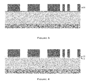
- FIG. 1-76 are illustrations of a semiconductor substrate, following a sequence of processing steps, the result of each processing step being depicted in cross-section.
- FIG. 77 illustrates a semiconductor substrate, following a the application of multiple metal layer steps, the result being depicted in cross-section.
- CMOS processes are finely tuned, complex processes that are very sensitive to being broken if changes are made.
- Intel Corporation addresses this sensitivity with its slogan, “Copy exactly.” In other words, even the slightest of changes can disrupt the entire process and require a re-tuning of that process.
- Various individual process steps and sequences are likewise very sensitive to being disrupted.
- Some of the most delicate parts of the process include the silicon surface preparation of the areas of the substrate where the channels of MOS transistors are going to be put. These surfaces must be kept near perfect to avoid current leakage paths and recombination sites that would degrade performance.
- Another sensitive stage is following the formation of salicided contacts to the MOS transistors as these contacts are easily damaged after formation by elevated temperatures (e.g., a temperature of 800° C. or higher).
- a non-volatile memory array benefits if that array can be very compact.
- the most compact memory arrays have a 4F 2 memory cell size.
- a 4F 2 memory array is achieved with a diode matrix wherein the diodes are formed in the vertical orientation.
- these diodes must have low leakage to prevent unnecessary power loss.
- an epi-silicon diode formation process will yield the highest quality diodes.
- epi-silicon is grown at elevated temperatures.
- the present invention is a means of incorporating an epi-silicon (or poly-silicon), non-volatile diode memory array within a CMOS process without compromising the performance or characteristics of the resulting CMOS logic.
- the present invention is an epi-silicon process sequence that is introduced into a standard CMOS process (i) after the MOS transistors' gate oxide is formed and the gate poly-silicon is deposited (thereby protecting the delicate surface areas of the MOS transistors) and (ii) before the salicided contacts to those MOS transistors are formed (thereby performing any newly introduced steps having an elevated temperature, such as any epi-silicon or poly-silicon deposition for the formation of diodes, prior to the formation of that salicide).
- This timing of the diode formation steps has the additional advantage that the diode top contacts may also be provided with a salicided contact.
- CMOS process is outlined up to the metalization steps, with the steps of the present invention included therein. All of these steps are well understood by those skilled in the art of semiconductor manufacturing. Many of the steps outlined herein will have alternate approaches, process tools, chemistries, and the like for accomplishing the same result.
- the steps outlined herein as well as the Figures are an example of the preferred embodiment of the invention and have been presented for the purposes of illustration and description. They are not intended to limit the invention to the precise steps disclosed. The Figures are not in scale.
- an initial substrate 10 is shown in cross-section.
- This substrate consists of a layer of P ⁇ epi-silicon 12 grown upon a P + silicon substrate 11 .
- a very thin layer of thermal silicon dioxide 13 is grown on this epi substrate. This oxide acts as a stress relief layer between the substrate and a subsequent nitride layer.
- FIG. 2 shows the substrate in cross section following the deposition of Silicon Nitride (SiN x ) 21 .
- This SiN x layer is deposited using Chemical Vapor Deposition (CVD). This layer serves as a polish stop layer during the formation of shallow trench isolation.
- CVD Chemical Vapor Deposition
- FIG. 3 shows the substrate in cross section following spin-on, exposure, and development of photoresist 31 for the definition of STI trenches.
- This is a critical mask and it incorporates the new features of the diode array bit-lines (which are a line-and-space pattern at the critical dimension), however the processing steps remain the same as a standard CMOS process without the inclusion of the present invention.
- FIG. 4 shows the substrate in cross section following the etching of the SiN x 21 and Pad Oxide 13 .
- a reactive ion etch (RIE) utilizing fluorine chemistry is used.
- FIG. 5 shows the substrate in cross section following the etching of the STI trenches 31 into the silicon substrate.
- a reactive ion etch (RIE) utilizing fluorine chemistry is used.
- the STI defines the transistor active areas and the diode array bit-lines.
- FIG. 6 shows the substrate in cross section following photoresist removal. An oxygen plasma is used to burn off any remaining photoresist.
- FIG. 7 shows the substrate in cross section following the filling of the STI trenches with oxide 71 .
- This oxide layer is deposited using CVD to conformally fill the STI trenches.
- the oxide will electrically isolate the transistors in the circuit as well as the bit-lines.
- FIG. 8 shows the substrate in cross section following planarization of the STI trench oxide.
- the surface oxide is removed using Chemical Mechanical Polishing (CMP).
- CMP Chemical Mechanical Polishing
- the CMP process is formulated to stop (i.e., significantly slow down) when it hits silicon nitride.
- FIG. 9 shows the substrate in cross section following the removal of silicon nitride.
- a wet etch in hot phosphoric acid (H 3 PO 4 ) is used to complete formation of the STI.
- An HF dip removes surface oxide.
- FIG. 10 shows the substrate in cross section following the spin-on, exposure, and development of photoresist 101 for N-well formation. This will help to form the PMOS transistors.
- the N-wells are patterned with a non-critical mask and thicker resist to block the subsequent implant.
- FIG. 11 shows the substrate in cross section during N-well implantation.
- a deep (high-energy) implant of phosphorous ions creates a localized N-type region 111 for the PMOS transistor.
- FIG. 12 shows the substrate in cross section following photoresist removal. An oxygen plasma is used to burn off any remaining photoresist.
- FIG. 13 shows the substrate in cross section following the spin-on, exposure, and development of photoresist 131 for P-well formation. This will help to form the NMOS transistors.
- the P-wells are patterned with a non-critical mask and thicker resist to block the subsequent implant.
- the P-well for the bit-lines will be doped in parallel with the NMOS.
- FIG. 14 shows the substrate in cross section during P-well implantation.
- a deep (high-energy) implant of boron ions creates a localized P-type region 141 for the NMOS transistor.
- FIG. 15 shows the substrate in cross section following photoresist removal. An oxygen plasma is used to burn off any remaining photoresist.
- FIG. 16 shows the substrate in cross section following the annealing of the well implants.
- This step repairs damage to the silicon surface caused by the bombardment by implant ions and electrically activates the dopants. It also causes the dopants to spread somewhat deeper, but Rapid Thermal Annealing (RTA) can minimize this dopant spreading.
- RTA Rapid Thermal Annealing
- this step can be omitted if the thermal budget of the subsequent epi-silicon growth step is sufficient to effect this annealing operation.
- FIG. 17 shows the substrate in cross section following the growth of a sacrificial oxide 171 .
- This thin oxide layer is grown to capture defects in the silicon surface to create a more perfect surface for the formation of the gate regions for the MOS transistors.
- FIG. 18 shows the substrate in cross section following the remove of this sacrificial oxide.
- FIG. 19 shows the substrate in cross section following growth of a gate oxide 191 .
- a very thin oxide layer is grown that will serve as the gate dielectric for both transistors. It must be extremely clean, and is grown to a very precise thickness (+/ ⁇ 1 ⁇ ); it is to meet these requirements that the present invention does not change the CMOS process until after the following step of gate poly-silicon deposition.
- FIG. 20 shows the substrate in cross section following the deposition of the gate poly-silicon 201 .
- This poly-crystalline silicon layer is deposited using Chemical Vapor Deposition (CVD). Once deposited, the gate region and the gate oxide of the MOS transistors is protected. At this point, according to the present invention, the steps to incorporate the diode array can begin to be added.
- CVD Chemical Vapor Deposition
- FIG. 21 shows the substrate in cross section following spin-on, exposure, and development of photoresist 211 for the definition of the diode array areas. This is a non-critical mask step and it provides a large opening to expose the entire diode array. This is the first step incorporated solely to provide the benefit of the present invention. This is the first of up to three times that this diode array area mask is used.
- FIG. 22 shows the substrate in cross section following the etching away of the poly-silicon over the diode array areas 221 .
- This step is performed by a Reactive Ion Etch (RIE) in which a fluorine chemistry is used.
- RIE Reactive Ion Etch
- FIG. 23 shows the substrate in cross section during N-type implantation.
- An implant of phosphorous ions creates a localized N-type region 231 for the bit-lines.
- FIG. 24 shows the substrate in cross section following photoresist removal. An oxygen plasma is used to burn off any remaining photoresist.
- FIG. 25 shows the substrate in cross section following the deposition of Silicon Nitride (SiN x ).
- This SiN x layer 251 is deposited using Chemical Vapor Deposition (CVD). This layer serves as an etch stop layer during the formation of the diode holes prior to epi-silicon growth.
- CVD Chemical Vapor Deposition
- FIG. 26 shows the substrate in cross section following the deposition of a High Density Plasma (HDP) silicon dioxide 261 for the diode array areas. This is deposited using Chemical Vapor Deposition. It's thickness should allow for the height of the diodes desired after CMP steps.
- HDP High Density Plasma
- FIG. 27 shows the substrate in cross section following planarization of the HDP diode array area oxide.
- the surface oxide is removed using Chemical Mechanical Polishing (CMP).
- CMP Chemical Mechanical Polishing
- This CMP process is a timed step.
- the gate poly-silicon thickness could be matched to the diode height enabling this step to be is formulated to stop (i.e., significantly slow down) when it hits the layer of silicon nitride.
- FIG. 28 shows the substrate in cross section following deposition of a hard-mask poly-silicon layer 281 .
- This poly-crystalline silicon layer is deposited using Chemical Vapor Deposition (CVD).
- CVD Chemical Vapor Deposition
- This poly-silicon layer will provide an etch mask during the deep hole etch for forming the diodes. It's presence is typically required because the holes to form the diodes are printed at the critical geometry and therefore will require a thin photoresist layer to print; since the holes are etched deep, the photoresist may be etched away before the holes are fully etched and this hard mask will provide the extra etch time to complete the hole etch.
- FIG. 29 shows the substrate in cross section following spin-on, exposure, and development of photoresist 291 for the definition of the diode array diode holes. This is the one critical mask step introduced according to the present invention and it provides a small hole for each diode in the diode array.
- FIG. 30 shows the substrate in cross section following the etching through of the poly-silicon hard mask and the etching through of the HDP oxide to form holes 301 for all of the diodes in the diode array areas.
- This step is performed by a Reactive Ion Etch (RIE) in which two fluorine chemistries are used—the first chemistry is selective to etch poly-silicon and the second selectively etches oxide preferentially over both silicon and silicon nitride.
- RIE Reactive Ion Etch
- FIG. 31 shows the substrate in cross section following the etching through of the silicon nitride layer 251 over the bit-lines in the diode array areas. This step is performed by a Reactive Ion Etch (RIE) in which a fluorine chemistry is used.
- RIE Reactive Ion Etch
- FIG. 32 shows the substrate in cross section following the etching through of the silicon oxide gate oxide layer 191 over the bit-lines in the diode array areas. This step is performed by a Reactive Ion Etch (RIE) in which a fluorine chemistry is used.
- RIE Reactive Ion Etch
- FIG. 33 shows the substrate in cross section following the removal of the poly-silicon hard mask 281 .
- This can be performed by a Reactive Ion Etch (RIE) in which a fluorine chemistry is used or etched by wet chemistry.
- RIE Reactive Ion Etch
- this poly-silicon removal step can be performed prior to the etching through of the silicon oxide gate oxide layer (or prior to the etching through of both the silicon nitride layer and the silicon oxide gate oxide layer).
- FIG. 34 shows the substrate in cross section following epitaxial silicon growth.
- This epi-silicon growth is a selective epi-silicon growth step and, as such, new silicon 341 only forms on existing silicon (hence, the poly-silicon of the hard mask must be fully removed to prevent undesired silicon growth).
- This epi-silicon is formed at elevated temperatures (500° C.-900° C.) and, according to the present invention, must be performed prior to salicide contact formation on the MOS transistor gates, sources and drains.
- FIG. 35 shows the substrate in cross section following planarization of the epi-silicon diode array area diodes.
- the surface epi-silicon is removed using Chemical Mechanical Polishing (CMP). This CMP process is run until the remaining gate poly-silicon is exposed. This step completes the formation of the body of the diodes of the memory arrays. All that remains to complete the diodes is to implant the anode areas of the diodes.
- CMP Chemical Mechanical Polishing
- FIG. 36 shows the substrate in cross section following spin-on, exposure, and development of the photoresist 361 to define the transistor gate electrodes. This is the most critical patterning step in the CMOS part of the process. Precise sizing of the poly gate length is a first-order determinant of transistor switching speed. The highest resolution patterning systems are used (i.e. DUV) along with a thin layer of photoresist due to the critical nature of the layer.
- FIG. 37 shows the substrate in cross section following the etch of the gate poly-silicon.
- a Reactive Ion Etch (RIE) utilizing fluorine chemistry is used.
- the PMOS transistor gates 371 are formed in the same step as the NMOS transistor gates 372 . The completes the formation of the “gate stack.”
- FIG. 38 shows the substrate in cross section following photoresist removal. An oxygen plasma is used to burn off any remaining photoresist.
- FIG. 39 shows the substrate in cross section following oxidization of the gate poly-silicon.
- a thin layer of oxide 391 is grown on top of the poly-silicon gate (and upon any exposed silicon) to act as a buffer between the poly-silicon and a subsequent silicon nitride layer.
- FIG. 40 shows the substrate in cross section following spin-on, exposure, and development of the photoresist 401 to define the NMOS transistor tip implant.
- the “tip” serves to reduce hot electron effects near the gate regions in the NMOS transistors.
- FIG. 41 shows the substrate in cross section during the NMOS transistor tip implant: A very shallow (low energy) and low dose implant of arsenic ions begins the formation of the NMOS transistor source and drain regions and implants the NMOS transistor tip implant 411 .
- FIG. 42 shows the substrate in cross section following photoresist removal. An oxygen plasma is used to burn off any remaining photoresist.
- FIG. 43 shows the substrate in cross section following spin-on, exposure, and development of the photoresist 431 to define the PMOS transistor tip implant.
- the “tip” serves to reduce hot electron effects near the gate regions in the PMOS transistors.
- FIG. 44 shows the substrate in cross section following during the NMOS transistor tip implant: A very shallow (low energy) and low dose implant of BF 2 ions begins the formation of the PMOS transistor source and drain regions and implants the PMOS transistor tip implant 441 .
- FIG. 45 shows the substrate in cross section following photoresist removal. An oxygen plasma is used to burn off any remaining photoresist.
- FIG. 46 shows the substrate in cross section following the deposition of a silicon nitride layer 461 using Chemical Vapor Deposition (CVD). This is the first step of forming a nitride spacer as is well known in the art.
- CVD Chemical Vapor Deposition
- FIG. 47 shows the substrate in cross section following a timed nitride etch to form spacer sidewalls 471 .
- This is a carefully controlled Reactive Ion Etch (RIE) etch that removes the thin nitride from the horizontal surfaces, but will leave the sidewalls 471 .
- RIE Reactive Ion Etch
- FIG. 48 shows the substrate in cross section following the spin-on, exposure, and development of the photoresist 481 to define the NMOS transistor source and drain implant. This is a non-critical mask.
- FIG. 49 shows the substrate in cross section during the NMOS transistors' source and drain implant 491 .
- a shallow and high-dose implant of arsenic ions creates a heavily-doped NMOS transistor source and drain.
- the spacer shields this implant from falling too near to the channel region.
- FIG. 50 shows the substrate in cross section following photoresist removal.
- An oxygen plasma is used to burn off any remaining photoresist.
- FIG. 51 shows the substrate in cross section following the spin-on, exposure, and development of the photoresist 511 to define the PMOS transistor source and drain implant. This is a non-critical mask.
- FIG. 52 shows the substrate in cross section during the PMOS transistors' source and drain implant 521 .
- a shallow and high-dose implant of BF 2 ions creates a heavily-doped PMOS transistor source and drain.
- the spacer shields this implant from falling too near to the channel region.
- FIG. 53 shows the substrate in cross section following photoresist removal. An oxygen plasma is used to burn off any remaining photoresist.
- FIG. 54 shows the substrate in cross section following the spin-on, exposure, and development of the photoresist 541 to define the diode's anode implant. This is the second use of this non-critical mask. Note that by fine-tuning the thickness of the photoresist for the PMOS transistors' source and drain implant step, this photo step and the subsequent implant and resist strip steps might be eliminated.
- FIG. 55 shows the substrate in cross section during the diodes' anode implant.
- a shallow and high-dose implant of BF 2 ions creates a heavily-doped anode 551 on the diodes.
- FIG. 56 shows the substrate in cross section following photoresist removal. An oxygen plasma is used to burn off any remaining photoresist.
- FIG. 57 shows the substrate in cross section following the annealing of the MOS transistors' source and drain implants and the diodes' anode implants.
- RTA Rapid Thermal Annealing
- FIG. 58 shows the substrate in cross section following the stripping of the surface oxides.
- a quick dip in HF will remove any exposed gate oxide and expose bare silicon in the source, the poly-silicon gate, and the drain areas. Any native oxide that may have formed upon the diode anodes will likewise be removed.
- FIG. 59 shows the substrate in cross section following the deposition of a thin layer of Titanium 591 by sputtering across the entire wafer surface.
- FIG. 60 shows the substrate in cross section following the formation of titanium silicide. This is done by Rapid Thermal Processing in nitrogen at 800° C. and causes the titanium to react with silicon, forming titanium silicide, where the titanium contacts silicon 601 . In other areas, the titanium is unaffected. This process perfectly aligns the silicide to the exposed silicon, and is called Self-Aligned Silicide, or Salicide.
- FIG. 61 shows the substrate in cross section following a titanium etch: The unreacted titanium is removed using a wet etch in NH 4 OH+H 2 O 2 , but the titanium silicide remains. TiSi 2 provides an ohmic contact between silicon and subsequently deposited metal.
- FIG. 62 shows the substrate in cross section following field oxide deposition 621 . Through this oxide the contacts will be formed to connect to the transistors and to form cups to create the information storage elements.
- FIG. 63 shows the substrate in cross section following planarization of the field oxide.
- the surface oxide is removed using Chemical Mechanical Polishing (CMP).
- CMP Chemical Mechanical Polishing
- FIG. 64 shows the substrate in cross section following the spin-on, exposure, and development of photoresist 641 for the definition of the contacts.
- This is a critical mask and it incorporates the new fine geometry features of the diode array cups. While a contact mask is present in a standard CMOS process without the inclusion of the present invention, this mask might not require the most critical geometry features in a standard CMOS process without the inclusion of the present invention. However, since the transistor contacts can be larger than the critical geometry and the diode contacts have a salicide contact which is very conductive, some misalignment can be tolerated.
- FIG. 65 shows the substrate in cross section following the contact etch: A carefully designed Reactive Ion Etch (RIE) etch using fluorine chemistry is used to achieve vertical sidewalls, as is well known to those skilled in the art.
- RIE Reactive Ion Etch
- FIG. 66 shows the substrate in cross section following photoresist removal. An oxygen plasma is used to burn off any remaining photoresist.
- FIG. 67 shows the substrate in cross section following the deposition of titanium nitride (TiN) 671 .
- a sputterer or Atomic Layer Deposition (ALD) is used to deposit a thin adhesion layer of TiN. This layer will help the subsequent tungsten layer to stick to the oxide.
- FIG. 68 shows the substrate in cross section following the deposition of tungsten 681 .
- Tungsten is used because it has good conductivity and it deposits conformally (via CVD) and can fill the contact holes.
- the tungsten thickness must be at least half of the diameter of the contact hole.
- FIG. 69 shows the substrate in cross section following the planarization of the tungsten.
- CMP is used to remove the surface tungsten.
- the surface titanium nitride is also removed as well.
- the remaining tungsten forms contact “plugs”. These contact plugs are the contacts that are used to connect the transistor contacts and non-memory diode contacts to the metal interconnects that will be formed during the back end of line (BEOL) processing.
- BEOL back end of line
- FIG. 70 shows the substrate in cross section following the spin-on, exposure, and development of the photoresist 701 to once again define the diode array areas for the formation of the information storage elements. This is the third and final use of this non-critical mask. Note that if diodes other than memory cell diodes are present in the array formation (i.e., diodes for which an information storage element is not desired), then a new mask will have to be created so as to mask away any diodes not having an information storage element.
- FIG. 71 shows the substrate in cross section following a tungsten etch.
- An RIE etch will selectively remove the tungsten on top of the memory diodes, leaving the field oxide and forming cups 711 where information storage elements are to be formed.
- FIG. 72 shows the substrate in cross section following photoresist removal. An oxygen plasma is used to burn off any remaining photoresist.
- FIG. 73 shows the substrate in cross section following the deposition of a silicon nitride layer 731 using Chemical Vapor Deposition (CVD). This is the same as the first step of forming a nitride spacer as is well known in the art.
- CVD Chemical Vapor Deposition
- FIG. 74 shows the substrate in cross section following a timed nitride etch to form spacer sidewalls.
- This is a carefully controlled Reactive Ion Etch (RIE) etch that removes the thin nitride from the horizontal surfaces, but will leave the silicon nitride on the lower sidewalls of the cups.
- RIE Reactive Ion Etch
- FIG. 75 shows the substrate in cross section following sputter deposition or MOCVD deposition of a phase-change material 751 such as a Chalcogenide alloy such as GST. (i.e., an alloy of elements including Germanium, Tellurium and Antimony).
- a Chalcogenide alloy such as GST.
- the Chalcogenide alloy thickness must be at least half of the diameter of the contact hole.
- FIG. 76 shows the substrate in cross section following the planarization of the Chalcogenide alloy.
- CMP is used to remove the surface Chalcogenide alloy.
- the resulting surface will have contact points of tungsten (at the device contacts) and GST (at the information storage elements 0.
- FIG. 77 shows the substrate in cross section following two back end of line (BEOL) metal layers of interconnects.
- BEOL back end of line
- the present example figures also presumes that the source and drain contacts to the PMOS transistor and the gate contact to the NMOS transistor are formed in a plane other than that plane of the cross-section of the figures and are therefore not depicted.
- the interconnect would be followed by the formation of the bond pads and passivation. All of this, as well as the specifics of the many individual process steps described above, are all well understood by those skilled in the art.
- a key aspect of the present invention is the ordering of the steps such that the transistors and the diodes are formed with salicided contacts while the phase-change material is not subjected to high (above 800° C.) temperatures.
- Devices constructed according to the present invention can be incorporated into memory card controller chips so as to combine the functions of the controller with the information storage circuitry in a single chip. Devices so constructed will find applicability in such areas as memory devices for storing digital text, digital books, digital music, digital audio, digital photography (wherein one or more digital still images can be stored including sequences of digital images), digital video, and digital cartography (wherein one or more digital maps can be stored), as well as any combinations thereof. These devices can be removable or removable and interchangeable among electronic systems that use memory cards.
- They can be packaged in any variety of industry standard form factors including Compact Flash, Secure Digital, MultiMedia Cards, PCMCIA Cards, Memory Stick, any of a large variety of integrated circuit packages including Ball Grid Arrays, Dual In-Line Packages (DIP's), SOIC's, PLCC, TQFP's and the like, as well as in custom designed packages.
- These packages can contain just the combined controller with memory chip, multiple memory chips, one or more memory chips along with other logic devices or other storage devices such as PLD's, PLA's, micro-controllers, microprocessors or chip-sets or other custom or standard circuitry.
Abstract
Description
Claims (10)
Priority Applications (3)
| Application Number | Priority Date | Filing Date | Title |
|---|---|---|---|
| US14/306,801 US9054031B2 (en) | 2011-12-08 | 2014-06-17 | Embedded non-volatile memory |
| US14/733,919 US9431460B2 (en) | 2011-12-08 | 2015-06-08 | Embedded non-volatile memory |
| US15/236,600 US9812503B2 (en) | 2011-12-08 | 2016-08-15 | Embedded non-volatile memory |
Applications Claiming Priority (4)
| Application Number | Priority Date | Filing Date | Title |
|---|---|---|---|
| US201161630297P | 2011-12-08 | 2011-12-08 | |
| US201261632393P | 2012-01-20 | 2012-01-20 | |
| US13/707,895 US8786023B2 (en) | 2011-12-08 | 2012-12-07 | Embedded non-volatile memory |
| US14/306,801 US9054031B2 (en) | 2011-12-08 | 2014-06-17 | Embedded non-volatile memory |
Related Parent Applications (1)
| Application Number | Title | Priority Date | Filing Date |
|---|---|---|---|
| US13/707,895 Continuation US8786023B2 (en) | 2011-12-08 | 2012-12-07 | Embedded non-volatile memory |
Related Child Applications (1)
| Application Number | Title | Priority Date | Filing Date |
|---|---|---|---|
| US14/733,919 Continuation US9431460B2 (en) | 2011-12-08 | 2015-06-08 | Embedded non-volatile memory |
Publications (2)
| Publication Number | Publication Date |
|---|---|
| US20140335669A1 US20140335669A1 (en) | 2014-11-13 |
| US9054031B2 true US9054031B2 (en) | 2015-06-09 |
Family
ID=50879953
Family Applications (4)
| Application Number | Title | Priority Date | Filing Date |
|---|---|---|---|
| US13/707,895 Expired - Fee Related US8786023B2 (en) | 2011-12-08 | 2012-12-07 | Embedded non-volatile memory |
| US14/306,801 Active US9054031B2 (en) | 2011-12-08 | 2014-06-17 | Embedded non-volatile memory |
| US14/733,919 Active US9431460B2 (en) | 2011-12-08 | 2015-06-08 | Embedded non-volatile memory |
| US15/236,600 Active US9812503B2 (en) | 2011-12-08 | 2016-08-15 | Embedded non-volatile memory |
Family Applications Before (1)
| Application Number | Title | Priority Date | Filing Date |
|---|---|---|---|
| US13/707,895 Expired - Fee Related US8786023B2 (en) | 2011-12-08 | 2012-12-07 | Embedded non-volatile memory |
Family Applications After (2)
| Application Number | Title | Priority Date | Filing Date |
|---|---|---|---|
| US14/733,919 Active US9431460B2 (en) | 2011-12-08 | 2015-06-08 | Embedded non-volatile memory |
| US15/236,600 Active US9812503B2 (en) | 2011-12-08 | 2016-08-15 | Embedded non-volatile memory |
Country Status (1)
| Country | Link |
|---|---|
| US (4) | US8786023B2 (en) |
Families Citing this family (1)
| Publication number | Priority date | Publication date | Assignee | Title |
|---|---|---|---|---|
| CN107546120B (en) * | 2016-06-24 | 2021-04-09 | 北大方正集团有限公司 | Metal electrode of diode, preparation method and diode |
Citations (3)
| Publication number | Priority date | Publication date | Assignee | Title |
|---|---|---|---|---|
| US20050223182A1 (en) | 2004-04-04 | 2005-10-06 | Guobiao Zhang | User-configurable pre-recorded memory |
| US20090267045A1 (en) * | 2008-04-28 | 2009-10-29 | Heon Yong Chang | Phase change memory device having heaters and method for manufacturing the same |
| US20100059731A1 (en) * | 2008-09-05 | 2010-03-11 | Heon Yong Chang | Phase change memory device and method for manufacturing the same |
Family Cites Families (5)
| Publication number | Priority date | Publication date | Assignee | Title |
|---|---|---|---|---|
| US6949424B2 (en) * | 2003-08-28 | 2005-09-27 | Texas Instruments Incorporated | Single poly-emitter PNP using DWELL diffusion in a BiCMOS technology |
| US7307327B2 (en) * | 2005-08-04 | 2007-12-11 | Micron Technology, Inc. | Reduced crosstalk CMOS image sensors |
| EP1809025A3 (en) * | 2006-01-17 | 2007-08-15 | STMicroelectronics (Research & Development) Limited | Memory enhanced image sensor |
| US8138049B2 (en) * | 2009-05-29 | 2012-03-20 | Silergy Technology | Fabrication of lateral double-diffused metal oxide semiconductor (LDMOS) devices |
| US8278690B2 (en) * | 2010-04-27 | 2012-10-02 | Omnivision Technologies, Inc. | Laser anneal for image sensors |
-
2012
- 2012-12-07 US US13/707,895 patent/US8786023B2/en not_active Expired - Fee Related
-
2014
- 2014-06-17 US US14/306,801 patent/US9054031B2/en active Active
-
2015
- 2015-06-08 US US14/733,919 patent/US9431460B2/en active Active
-
2016
- 2016-08-15 US US15/236,600 patent/US9812503B2/en active Active
Patent Citations (3)
| Publication number | Priority date | Publication date | Assignee | Title |
|---|---|---|---|---|
| US20050223182A1 (en) | 2004-04-04 | 2005-10-06 | Guobiao Zhang | User-configurable pre-recorded memory |
| US20090267045A1 (en) * | 2008-04-28 | 2009-10-29 | Heon Yong Chang | Phase change memory device having heaters and method for manufacturing the same |
| US20100059731A1 (en) * | 2008-09-05 | 2010-03-11 | Heon Yong Chang | Phase change memory device and method for manufacturing the same |
Also Published As
| Publication number | Publication date |
|---|---|
| US9812503B2 (en) | 2017-11-07 |
| US20160020253A1 (en) | 2016-01-21 |
| US20160351627A1 (en) | 2016-12-01 |
| US8786023B2 (en) | 2014-07-22 |
| US20140158963A1 (en) | 2014-06-12 |
| US9431460B2 (en) | 2016-08-30 |
| US20140335669A1 (en) | 2014-11-13 |
Similar Documents
| Publication | Publication Date | Title |
|---|---|---|
| US10861700B2 (en) | Diode array for connecting to phase change memory and method forming same | |
| US9947528B2 (en) | Structure and method for nFET with high k metal gate | |
| US9514976B2 (en) | Trench isolation implantation | |
| JP5116294B2 (en) | Semiconductor structure and manufacturing method thereof (vertical SOI trench SONOS cell) | |
| CN104051343B (en) | Transistor with the deep N-well being implanted by grid | |
| KR20150088230A (en) | Structure and method for single gate non-volatile memory device | |
| US11616064B2 (en) | Semiconductor structure | |
| US10840253B2 (en) | Increased gate coupling effect in multigate transistor | |
| US10276582B2 (en) | High coupling ratio split gate memory cell | |
| US9871032B2 (en) | Gate-grounded metal oxide semiconductor device | |
| US7888200B2 (en) | Embedded memory in a CMOS circuit and methods of forming the same | |
| US20160172314A1 (en) | Structure to prevent deep trench moat charging and moat isolation fails | |
| US6949467B2 (en) | Forming method of contact in semiconductor device and manufacturing method of PMOS device using the same | |
| US7868388B2 (en) | Embedded memory in a CMOS circuit and methods of forming the same | |
| US10395987B2 (en) | Transistor with source-drain silicide pullback | |
| US9812503B2 (en) | Embedded non-volatile memory | |
| CN109461657B (en) | Substrate contact for transistor | |
| US20210384202A1 (en) | Semiconductor structure and method of forming the same | |
| US7767577B2 (en) | Nested and isolated transistors with reduced impedance difference |
Legal Events
| Date | Code | Title | Description |
|---|---|---|---|
| AS | Assignment |
Owner name: CONTOUR SEMICONDUCTOR, INC., MASSACHUSETTS Free format text: ASSIGNMENT OF ASSIGNORS INTEREST;ASSIGNORS:SHEPARD, DANIEL R.;APODACA, MAC D.;TRENT, THOMAS MICHAEL;AND OTHERS;SIGNING DATES FROM 20130103 TO 20130107;REEL/FRAME:033121/0017 |
|
| FEPP | Fee payment procedure |
Free format text: PAYOR NUMBER ASSIGNED (ORIGINAL EVENT CODE: ASPN); ENTITY STATUS OF PATENT OWNER: LARGE ENTITY |
|
| STCF | Information on status: patent grant |
Free format text: PATENTED CASE |
|
| AS | Assignment |
Owner name: HGST NETHERLANDS B.V., NETHERLANDS Free format text: ASSIGNMENT OF ASSIGNORS INTEREST;ASSIGNOR:CONTOUR SEMICONDUCTOR, INC.;REEL/FRAME:035748/0909 Effective date: 20150515 |
|
| AS | Assignment |
Owner name: HGST, INC., CALIFORNIA Free format text: CORRECTIVE ASSIGNMENT TO CORRECT THE NAME AND ADDRESS OF THE ASSIGNEE PREVIOUSLY RECORDED ON REEL 035748 FRAME 0909. ASSIGNOR(S) HEREBY CONFIRMS THE NAME AND ADDRESS OF THE ASSIGNEE SI HGST, INC.,3403 YERBA BUENA ROAD,SAN JOSE, CA 95135;ASSIGNOR:CONTOUR SEMICONDUCTOR, INC.;REEL/FRAME:035831/0594 Effective date: 20150515 |
|
| CC | Certificate of correction | ||
| AS | Assignment |
Owner name: JPMORGAN CHASE BANK, N.A., AS COLLATERAL AGENT, IL Free format text: SECURITY AGREEMENT;ASSIGNOR:HGST, INC.;REEL/FRAME:039389/0684 Effective date: 20160712 |
|
| AS | Assignment |
Owner name: HGST, INC., CALIFORNIA Free format text: RELEASE BY SECURED PARTY;ASSIGNOR:JPMORGAN CHASE BANK, N.A., AS COLLATERAL AGENT;REEL/FRAME:039689/0950 Effective date: 20160719 |
|
| AS | Assignment |
Owner name: WESTERN DIGITAL TECHNOLOGIES, INC., CALIFORNIA Free format text: ASSIGNMENT OF ASSIGNORS INTEREST;ASSIGNOR:HGST, INC.;REEL/FRAME:046939/0587 Effective date: 20180824 |
|
| MAFP | Maintenance fee payment |
Free format text: PAYMENT OF MAINTENANCE FEE, 4TH YEAR, LARGE ENTITY (ORIGINAL EVENT CODE: M1551); ENTITY STATUS OF PATENT OWNER: LARGE ENTITY Year of fee payment: 4 |
|
| AS | Assignment |
Owner name: WESTERN DIGITAL TECHNOLOGIES, INC., CALIFORNIA Free format text: RELEASE OF SECURITY INTEREST AT REEL 039389 FRAME 0684;ASSIGNOR:JPMORGAN CHASE BANK, N.A.;REEL/FRAME:058965/0535 Effective date: 20220203 |
|
| MAFP | Maintenance fee payment |
Free format text: PAYMENT OF MAINTENANCE FEE, 8TH YEAR, LARGE ENTITY (ORIGINAL EVENT CODE: M1552); ENTITY STATUS OF PATENT OWNER: LARGE ENTITY Year of fee payment: 8 |
|
| AS | Assignment |
Owner name: JPMORGAN CHASE BANK, N.A., ILLINOIS Free format text: PATENT COLLATERAL AGREEMENT - A&R LOAN AGREEMENT;ASSIGNOR:WESTERN DIGITAL TECHNOLOGIES, INC.;REEL/FRAME:064715/0001 Effective date: 20230818 Owner name: JPMORGAN CHASE BANK, N.A., ILLINOIS Free format text: PATENT COLLATERAL AGREEMENT - DDTL LOAN AGREEMENT;ASSIGNOR:WESTERN DIGITAL TECHNOLOGIES, INC.;REEL/FRAME:067045/0156 Effective date: 20230818 |