US9024664B2 - Current-to-voltage converter and electronic apparatus thereof - Google Patents
Current-to-voltage converter and electronic apparatus thereof Download PDFInfo
- Publication number
- US9024664B2 US9024664B2 US14/018,457 US201314018457A US9024664B2 US 9024664 B2 US9024664 B2 US 9024664B2 US 201314018457 A US201314018457 A US 201314018457A US 9024664 B2 US9024664 B2 US 9024664B2
- Authority
- US
- United States
- Prior art keywords
- current
- voltage
- bias
- bias circuit
- type transistor
- Prior art date
- Legal status (The legal status is an assumption and is not a legal conclusion. Google has not performed a legal analysis and makes no representation as to the accuracy of the status listed.)
- Active
Links
Images


Classifications
-
- H—ELECTRICITY
- H03—ELECTRONIC CIRCUITRY
- H03F—AMPLIFIERS
- H03F3/00—Amplifiers with only discharge tubes or only semiconductor devices as amplifying elements
- H03F3/34—DC amplifiers in which all stages are DC-coupled
- H03F3/343—DC amplifiers in which all stages are DC-coupled with semiconductor devices only
- H03F3/345—DC amplifiers in which all stages are DC-coupled with semiconductor devices only with field-effect devices
-
- H—ELECTRICITY
- H02—GENERATION; CONVERSION OR DISTRIBUTION OF ELECTRIC POWER
- H02M—APPARATUS FOR CONVERSION BETWEEN AC AND AC, BETWEEN AC AND DC, OR BETWEEN DC AND DC, AND FOR USE WITH MAINS OR SIMILAR POWER SUPPLY SYSTEMS; CONVERSION OF DC OR AC INPUT POWER INTO SURGE OUTPUT POWER; CONTROL OR REGULATION THEREOF
- H02M1/00—Details of apparatus for conversion
Definitions
- the present disclosure is related to a current-to-voltage converter, and in particular to, a single stage current-to-voltage converter with a high input range and a wide output swing, and the electronic apparatus using the current-to-voltage converter.
- an electronic apparatus usually has a current-to-voltage converter, and the current-to-voltage converter can convert the current to the voltage, and transmit the converted voltage to the other function circuit of the electronic apparatus, such that the function circuit can receive the voltage, and execute a corresponding function according to the voltage.
- FIG. 1 is circuit diagram of a conventional current-to-voltage converter.
- the conventional current-to-voltage converter 1 comprises a first current-to-voltage unit 11 , a second current-to-voltage unit 12 and an output capacitor Cout, and has an input end at an end E and an output end at an end F.
- the first current-to-voltage unit 11 and the second current-to-voltage unit 12 are connected to each other through the ends E and F, and thus form a cascode structure.
- the output capacitor Cout is connected to an output end of the conventional current-to-voltage converter 1 through the end F.
- the conventional current-to-voltage converter 1 can receive an input current through an input end thereof, generate the voltage Vout according to the current Iin, and output the voltage Vout through the output end thereof.
- the first current-to-voltage unit 11 and the second current-to-voltage unit 12 determine currents flowing inner transistors thereof according to the current Iin, and the currents flowing the inner transistors thereof determine the drain-source voltages of the inner transistors of the first current-to-voltage unit 11 and the second current-to-voltage unit 12 , such that the voltage Vout at the output end can be determined.
- the first current-to-voltage unit 11 comprises four P-type transistors P 1 through P 4 , an N-type transistor N 1 , and an operation amplifier OP 1 .
- Gates of the P-type transistors P 1 and P 2 are connected to each other, and further to a drain of the P-type transistor P 3 .
- Sources of P-type transistors P 1 and P 2 are connected to a supply voltage VDD.
- a positive input end of the operation amplifier OP 1 is connected to a drain of the P-type transistor P 1 and a source of the P-type transistor P 3 .
- a negative input end of the operation amplifier OP 1 is connected to a drain of the P-type transistor P 2 and a source of the P-type transistor P 4 .
- a gate of the P-type transistor P 3 is connected to a bias bias 1
- an output end of the operation amplifier OP 1 is connected to a gate of the P-type transistor P 4 .
- a drain of the N-type transistor N 1 is connected to a drain of the P-type transistor P 3
- a gate of the N-type transistor N 1 is connected to another bias biasa.
- a source of the N-type transistor N 1 and a drain of the P-type transistor P 4 are respectively connected to the ends E and F.
- the second current-to-voltage unit 12 comprises four N-type transistors N 2 through N 5 , a P-type transistor P 5 , and an operation amplifier OP 2 .
- Gates of the N-type transistors N 2 and N 3 are connected to each other, and further to a drain of the N-type transistor N 4 .
- Sources of the N-type transistors N 1 and N 2 are connected to a ground.
- a positive input end of the operation amplifier OP 2 is connected to a drain of the N-type transistor N 2 and a source of the N-type transistor N 4 .
- a negative input end of the operation amplifier OP 2 is connected to a drain of the N-type transistor N 3 and a source of the N-type transistor N 5 .
- a gate of the N-type transistor N 4 is connected a bias bias 2 , and an output end of the operation amplifier OP 2 is connected to gate of the N-type transistor N 5 .
- a drain of the P-type transistor P 5 is connected to a drain of the N-type transistor N 4 , and a gate of the P-type transistor P 5 is connected to another bias biasb.
- a source of the P-type transistor P 5 and a drain of the N-type transistor N 5 are respectively connected to the ends E and F.
- the biases bias 1 and bias 2 are respectively used to determine swings of currents generated by the first current-to-voltage unit 11 and the second current-to-voltage unit 12 , and the swings of the currents generated by the first current-to-voltage unit 11 and the second current-to-voltage unit 12 determines the swing of voltage Vout.
- the bias bias 1 and bias 2 are fixed biases (i.e. constant voltage), such that when the current Iin is not input to the first current-to-voltage unit 11 and the second current-to-voltage unit 12 , the fixed currents flowing the P-type transistors P 2 , P 4 , and the N-type transistors N 5 , N 3 are generated.
- the gate of N-type transistor N 1 and the gate of the P-type transistor P 5 should be connected to the biases biasa and biasb, and the input range of the current Iin is limited.
- the operation amplifier OP 1 is used to clamp the voltage levels of the ends A and B at the constant voltage values
- the operation amplifier OP 2 is used to clamp the voltage levels of the ends C and D at the constant voltage values. Accordingly, the operation amplifiers OP 1 and OP 2 can enhance the output impedance of the output end of the conventional current-to-voltage converter 1 , so as to reduce the effect which the leakage current affects the voltage Vout.
- the operation bandwidth of the operation amplifiers OP 1 and OP 2 may decrease the current tracking speeds of the currents flowing the P-type transistors P 2 , P 4 , and the N-type transistors N 5 , N 3 , such that the transient speed of the voltage Vout of the output end may be too slow to cause the current-to-voltage (Iin-to-Vout) conversion error, i.e. the rising or falling speed of the currents flowing the P-type transistors P 2 , P 4 , and the N-type transistors N 5 , N 3 may be slow unexpectedly, and the rising or falling speed of the voltage Vout is not fast enough.
- Iin-to-Vout current-to-voltage
- An exemplary embodiment of the present disclosure provides a current-to-voltage converter.
- the current-to-voltage converter is used to receive an input current, and accordingly generates an output voltage.
- the current-to-voltage converter comprises a current tracking bias circuit, a current-to-voltage unit, and a voltage clamp bias circuit, wherein the current-to-voltage unit is connected to the current tracking bias circuit, and the voltage clamp bias circuit is connected to current-to-voltage unit.
- the current tracking bias circuit generates a first bias according to the input current.
- the current-to-voltage unit receives the first bias and the input current, and generates the output voltage according to the input current, wherein the first bias determines a range of the input current, the current-to-voltage unit has a first current control device, and the first current control device changes a current conduction level thereof in response to the first bias, such that a rising or falling speed of the output voltage is enhanced.
- the voltage clamp bias circuit clamps voltage levels of two ends where the voltage clamp bias circuit is connected to the current-to-voltage unit.
- the current tracking bias circuit further generates a second bias according to the input current, and the current-to-voltage unit further receives the second bias.
- the current-to-voltage unit further has a second current control device, and the second current control device changes a current conduction level thereof according to the second bias to enhance the rising or falling speed of the output voltage.
- the voltage clamp bias circuit further clamps voltage levels of another two ends where the voltage clamp bias circuit is connected to the current-to-voltage unit, wherein the first bias and the second bias determine the range of the input current.
- An exemplary embodiment of the present disclosure provides an electronic apparatus comprising one of the above current-to-voltage converters and a function circuit, wherein the function circuit is connected to the current-to-voltage converter.
- the function circuit receives the output voltage, and executes a corresponding function accordingly.
- the current-to-voltage converter provided by the exemplary embodiment of the present disclosure can have the high input range and wide output swing by using the current tracking bias circuit and the voltage clamp bias circuit.
- the current-to-voltage unit of the current-to-voltage converter can have the current control device to enhance the rising or falling speed of the output voltage of the current-to-voltage converter.
- the voltage clamp bias circuit can further maintains the drain-source voltage of the transistor in the current-to-voltage unit with a constant voltage value, so as to reduce the effect which the channel length modulation effect of the transistor affects the output voltage of the current-to-voltage converter.
- FIG. 1 is circuit diagram of a conventional current-to-voltage converter.
- FIG. 2 is a block diagram of a current-to-voltage converter according to an exemplary embodiment of the present disclosure.
- FIG. 3 is a circuit diagram of a current-to-voltage converter according to an exemplary embodiment of the present disclosure.
- FIG. 4 is a block diagram of a current-to-voltage converter according to another exemplary embodiment of the present disclosure.
- FIG. 5 is a circuit diagram of a current-to-voltage converter according to another exemplary embodiment of the present disclosure.
- FIG. 6 is a circuit diagram of a current-to-voltage converter according to another exemplary embodiment of the present disclosure.
- FIG. 7 is a block diagram of an electronic apparatus according to an exemplary embodiment of the present disclosure.
- FIG. 2 is a block diagram of a current-to-voltage converter according to an exemplary embodiment of the present disclosure.
- the current-to-voltage converter 2 comprises a current tracking bias circuit 21 , a current-to-voltage unit 22 , a voltage clamp bias circuit 23 , and an output capacitor Cout. Two output ends of the current tracking bias circuit 21 are connected to two bias ends of the current-to-voltage unit 22 , and two ends of the current tracking bias circuit 21 are connected to two ends of the current-to-voltage unit 22 respectively.
- the four ends A through D of the current-to-voltage unit 22 are respectively connected to four ends of the voltage clamp bias circuit 23 , and another end of the voltage clamp bias circuit 23 is connected to the end F of the current-to-voltage unit 22 .
- An output end of the current-to-voltage converter 2 is located at the end F of the current-to-voltage unit 22 , an input end of the current-to-voltage converter 2 is connected to the end E of the current-to-voltage unit 22 , and the output capacitor Cout is connected between the end F and the ground.
- the current tracking bias circuit 21 biases bias 1 and bias 2 to the current-to-voltage unit 22 according to the current Iin. More specifically, the current tracking bias circuit 21 has a plurality of transistors to from two current mirrors, and is connected to the current-to-voltage unit 22 , such that the current tracking bias circuit 21 can generate currents corresponding to the current Iin, and then generate the biases bias 1 and bias 2 according to the generated currents. Since the biases bias 1 and bias 2 are generated according to current Iin, the input range of the current Iin input to the current-to-voltage converter 2 can be increased.
- the current-to-voltage unit 22 is used to receive the current Iin, and the biases bias 1 and bias 2 are used to determine the swings of the current generated by the current-to-voltage unit 22 .
- the current-to-voltage unit 22 generates the voltage Vout according to the received current Iin, and output the voltage Vout at the end F.
- the current-to-voltage unit 22 has two current control devices (not shown in FIG. 2 , but shown in the FIG. 3 , the devices CC 1 and CC 2 ), and the two control ends of the two current control devices are connected to the biases bias 1 and bias 2 .
- the first end of one current control device in the current-to-voltage unit 22 is connected to the end B
- the first end of the other one current control device in the current-to-voltage unit 22 is connected to the end D
- the second ends of the two current control device are connected to the end F.
- the current control device is controlled by the biases bias 1 and bias 2 , and the biases bias 1 and bias 2 are determined by the current Iin.
- the variations of the biases bias 1 and bias 2 are also changed, such that the current control device can increase the rising or falling speed of the currents generated by the current-to-voltage unit 22 to prevent from the current-to-voltage (Iin-to-Vout) conversion error owing to that the rising or falling speed of the voltage Vout cannot keep up with the variation of the current Iin.
- the voltage clamp bias circuit 23 has two operation amplifiers. Two positive input ends of the two operation amplifiers are connected to the ends A, C of the current-to-voltage unit 22 , and two negative input ends of the two operation amplifiers are connected to the ends B, D of the current-to-voltage unit 22 , such that the voltage level of the ends A through D are clamped at a constant voltage value.
- the output impedance of the current-to-voltage converter 2 is increased, and the leakage current is further decreased.
- the voltage levels of the ends A through D are constant voltage values, the effect owing to channel length modulation effect generated by the transistors of the current-to-voltage unit 22 is also decreased.
- the current-to-voltage converter 2 can have the high input range and wide output swing. Furthermore, by using the current control devices of the current-to-voltage unit 22 , the rising or falling speed of the voltage Vout of the output end of the current-to-voltage converter 2 can be further increased to prevent from the current-to-voltage (Iin-to-Vout) conversion error.
- FIG. 3 is a circuit diagram of a current-to-voltage converter according to an exemplary embodiment of the present disclosure.
- the current-to-voltage converter 3 in FIG. 3 is one implementation of the current-to-voltage converter 2 in FIG. 2 , but the present disclosure does not limit the implementation of the current-to-voltage converter 2 in FIG. 2 .
- the current-to-voltage converter 3 comprises a current tracking bias circuit 31 , a current-to-voltage unit 32 , a voltage clamp bias circuit 33 , and an output capacitor Cout.
- the functions and connections of the current tracking bias circuit 31 , the current-to-voltage unit 32 , the voltage clamp bias circuit 33 , and the output capacitor Cout are similar to those of the current tracking bias circuit 21 , the current-to-voltage unit 22 , the voltage clamp bias circuit 23 , and the output capacitor Cout, and thus the redundant description is omitted.
- the current tracking bias circuit 31 comprises two current mirrors, wherein one current mirror comprises two P-type transistors P 7 , P 8 , and two N-type transistors N 7 , N 8 , and the other one current mirror comprises two P-type transistors P 9 , P 10 , and two N-type transistors N 9 , N 10 .
- the current-to-voltage unit 32 comprise four P-type transistors P 1 through P 3 , P 5 , four N-type transistors N 1 through N 4 , and two current control devices CC 1 , CC 2 , wherein the current control devices CC 1 and CC 2 are respectively implemented by the P-type transistor P 6 and the N-type transistor N 6 .
- the voltage clamp bias circuit 33 comprises two operation amplifiers OP 1 , OP 2 , a P-type transistor P 4 , and an N-type transistor N 5 . It is noted that the implementation of the current control devices CC 1 and CC 2 does not limit the present disclosure, and the other components capable of controlling the current conduction levels thereof can be used to implement the current control devices CC 1 and CC 2 .
- Sources of the P-type transistors P 7 , P 8 are connected to the supply voltage VDD, gates of the N-type transistors N 7 and N 8 are connected to each other, and sources of the N-type transistors N 7 and N 8 are connected to the ground GND.
- a drain of the P-type transistor P 7 is connected to gates of the N-type transistors N 7 , N 8 , and a drain of the N-type transistor N 7 , and a gate of the P-type transistor P 7 is connected to gates of the P-type transistors P 1 , P 2 .
- a gate of the P-type transistor P 8 is connected to gates of the P-type transistors P 3 , P 6 , and a drain of the P-type transistor P 8 , and a drain of the N-type transistor N 8 is connected to a drain of the P-type transistor P 8 .
- Sources of the P-type transistors P 9 and P 10 are connected to the supply voltage VDD, gates of the P-type transistors P 9 and P 10 are connected to each other, and sources of the N-type transistors N 9 and N 10 are connected to the ground GND.
- a drain of the N-type transistor N 9 is connected to gates of the P-type transistors P 9 , P 10 , and a drain of the P-type transistor P 9 , a gate of the N-type transistor N 9 is connected to gates of the N-type transistors N 2 , N 3 .
- a gate of the N-type transistor N 10 is connected to gates of the N-type transistors N 4 , N 6 , and a drain of the N-type transistor N 10 , and a drain of the P-type transistor P 10 is connected to a drain of the N-type transistor N 10 .
- Sources of the P-type transistors P 1 , P 2 are connected to the supply voltage VDD, and gates of the P-type transistors P 1 , P 2 are connected to each other, and further to a drain of the P-type transistor P 3 .
- a drain of the P-type transistor P 1 is connected to a positive input end of the operation amplifier OP 1 and a source of the P-type transistor P 3 .
- a drain of the N-type transistor N 1 is connected to a drain of the P-type transistor P 3 , a gate of the N-type transistor N 1 is connected to the bias biasa, and a source of the N-type transistor N 1 is connected to the end E.
- a drain of the P-type transistor P 2 is connected to a negative input end of the operation amplifier OP 1 and sources of the P-type transistors P 4 , P 5 .
- An output end of the operation amplifier OP 1 is connected to a gate of the P-type transistor P 4 , and drains of the P-type transistors P 4 , P 5 are connected to the end F.
- Sources of the N-type transistors N 2 , N 3 are connected the ground GND, and gates of the N-type transistors N 2 , N 3 are connected to each other, and further to a drain of the N-type transistor N 4 .
- a drain of the N-type transistor N 2 is connected to a positive input end of the operation amplifier OP 2 and a source of the N-type transistor N 4 .
- a drain of the P-type transistor P 5 is connected to a drain of the N-type transistor N 4 , a gate of the P-type transistor P 5 is connected to the bias biasb, and a source of the P-type transistor P 5 is connected to the end E.
- a drain of the N-type transistor N 3 is connected to a negative end of the operation amplifier OP 2 and sources of the N-type transistors N 5 , N 6 .
- An output end of the operation amplifier OP 2 is connected to a gate of the N-type transistor N 5 , and drains of the N-type transistors N 5 , N 6 are connected to the end F.
- the current mirror formed by the P-type transistors P 7 , P 8 , and the N-type transistors N 7 , N 8 can mirror the input current Iin to generate the current corresponding to the current Iin, and generate the bias bias 1 to the gate of the P-type transistors P 3 and P 5 according to the generated current.
- the current mirror formed by the P-type transistors P 9 , P 10 , and the N-type transistors N 9 , N 10 can mirror the input current to generate the current corresponding to the current Iin, and generate the bias bias 2 to the gate of the N-type transistors N 4 and N 5 according to the generated current.
- the operation amplifier OP 1 is used to clamp the voltage levels of the ends A and B, and the operation amplifier OP 2 to clamp the voltage levels of the ends C and D, so as to reduce the effect which the leakage current affects the output swing of the voltage Vout. Additionally, since the voltages of the ends A through D are fixed, the drain-source voltages of the P-type transistors P 1 , P 2 , and the N-type transistors N 2 , N 3 are also fixed, such that the effect which the channel length modulation effect affects the voltage Vout output by the current-to-voltage converter 3 can be reduced.
- the P-type transistor P 6 and the N-type transistor N 6 are controlled by the biases bias 1 and bias 2 , the biases bias 1 and bias 2 are generated according to the current Iin, and thus current conduction levels of the P-type transistor P 6 and the N-type transistor N 6 are changed in response to the current Iin, so as to increase the rising or falling speed of the voltage Vout.
- FIG. 4 is a block diagram of a current-to-voltage converter according to another exemplary embodiment of the present disclosure.
- the current-to-voltage converter 4 comprises a current tracking bias circuit 41 , a current-to-voltage unit 42 , a voltage clamp bias circuit 43 , and an output capacitor Cout.
- the exemplary embodiment of FIG. 4 is mostly similar to the exemplary embodiment of FIG. 2 , and thus merely the differences between the exemplary embodiments of FIG. 2 and FIG. 4 are illustrated as follows.
- the current tracking bias circuit 41 merely has one output end connected to a bias end of the current-to-voltage unit 42 , and one end of the current tracking bias circuit 41 is connected to one end of the current-to-voltage unit 42 .
- the current tracking bias circuit 41 can merely generate the bias bias 1 to the current-to-voltage unit 42 according to the current Iin, and the current tracking bias circuit 21 has a plurality of transistors to form a current mirror.
- the voltage clamp bias circuit 43 merely clamps the voltage levels of the ends A and B.
- the current-to-voltage unit 42 merely has one current control device (not shown in FIG. 4 , but shown in FIG. 5 or FIG. 6 , the component CC 1 or CC 2 ), and the control end of the current control device is connected to the bias bias 1 , wherein the first end and the second end of the current control device are connected to the ends B and F respectively.
- FIG. 5 is a circuit diagram of a current-to-voltage converter according to another exemplary embodiment of the present disclosure.
- the current-to-voltage converter 5 in FIG. 5 is one implementation of the current-to-voltage converter 4 in FIG. 4 , but the present disclosure does not limit the implementation of the current-to-voltage converter 4 in FIG. 4 .
- the current-to-voltage converter 5 comprises a current tracking bias circuit 51 , a current-to-voltage unit 52 , a voltage clamp bias circuit 53 , and an output capacitor Cout.
- the functions and connections of the current tracking bias circuit 51 , the current-to-voltage unit 52 , voltage clamp bias circuit 53 , and the output capacitor Cout are similar to those of the current tracking bias circuit 41 , the current-to-voltage unit 42 , the voltage clamp bias circuit 43 , and the output capacitor Cout. Thus, the redundant description is omitted.
- the current tracking bias circuit 51 comprises two P-type transistors P 2 , P 3 , and two N-type transistors N 6 , N 7 to form a current mirror.
- the current-to-voltage unit 52 comprises two current sources CS 1 , CS 2 , a P-type transistor P 1 , three N-type transistors N 1 through N 3 , and a current control device CC 2 , wherein the current control device CC 2 is implemented by an N-type transistor N 5 .
- the voltage clamp bias circuit 53 comprises an operation amplifier OP 1 and an N-type transistor N 4 . It is noted that, the implementation of the current control device CC 2 is not used to limit the present disclosure, and the other component capable of controlling the current conduction level thereof can be used to implement the current control device CC 2 .
- Sources of the P-type transistors P 2 and P 3 are connected to the supply voltage VDD, gates of the P-type transistors P 2 and P 3 are connected to each other, and sources of the N-type transistors N 6 and N 7 are connected to the ground GND.
- a drain of the N-type transistor N 6 is connected to gates of the P-type transistors P 2 , P 3 , and a drain of the P-type transistor P 2 , and a gate of the N-type transistor N 6 is connected to gates of the N-type transistors N 1 , N 2 .
- a gate of the N-type transistor N 7 is connected to gates of the N-type transistors N 3 , N 5 , and a drain of the N-type transistor N 7 , and a drain of the P-type transistor P 3 is connected to a drain of the N-type transistor N 7 .
- Sources of the N-type transistors N 1 , N 2 are connected to the ground GND, and gates of the N-type transistors N 1 , N 2 are connected to each other, and further to a drain of the N-type transistor N 3 .
- a drain of the N-type transistor N 1 is connected to a positive input end of the operation amplifier OP 1 and a source of the N-type transistor N 3 .
- a drain of the P-type transistor P 1 is connected to a drain of the N-type transistor N 3 , a gate of the P-type transistor P 1 is connected to bias biasb, and a source of the P-type transistor P 1 is connected to the end E.
- a drain of the N-type transistor N 2 is connected to a negative input end of the operation amplifier OP 1 and sources of the N-type transistors N 4 , and N 5 .
- An output end of the operation amplifier OP 1 is connected to a gate of the N-type transistor N 4 , and drains of the N-type transistors N 4 , N 5 are connected to the end F.
- One end of the current source CS 1 is connected to the supply voltage VDD, and the other one end of the current source CS 1 is connected to the end E.
- One end of the current source CS 2 is connected to the supply voltage VDD, and the other one end of the current source CS 2 is connected to the end F.
- the current mirror formed by the P-type transistors P 2 , P 3 , and the N-type transistors N 6 , N 7 can mirror the input current Iin to generate the current corresponding to the current Iin, and generate the bias bias 1 to the gates of the N-type transistors N 3 and N 5 according to the generated current.
- the operation amplifier OP 1 is used to clamp the voltage levels of the ends A and B, so as to reduce the effect which the leakage current affects the output swing of the voltage Vout. Additionally, since the voltages of the ends A and B are fixed, the drain-source voltages of the N-type transistors N 1 , N 2 are also fixed, such that the effect which the channel length modulation effect affects the voltage Vout output by the current-to-voltage converter 5 can be reduced. Furthermore, the N-type transistor N 5 is controlled by the bias bias 1 , the bias bias 1 is generated according to the current Iin, and thus current conduction level of the N-type transistor N 5 is changed in response to the current Iin, so as to increase the rising or falling speed of the voltage Vout.
- FIG. 6 is a circuit diagram of a current-to-voltage converter according to another exemplary embodiment of the present disclosure.
- the current-to-voltage converter 6 in FIG. 6 is one implementation of the current-to-voltage converter 4 in FIG. 4 , but the present disclosure does not limit the implementation of the current-to-voltage converter 4 in FIG. 4 .
- the current-to-voltage converter 6 comprises a current tracking bias circuit 61 , a current-to-voltage unit 62 , a voltage clamp bias circuit 63 , and an output capacitor Cout.
- the functions and connections of the current tracking bias circuit 61 , the current-to-voltage unit 62 , the voltage clamp bias circuit 63 , and the output capacitor Cout are similar to those of the current tracking bias circuit 41 , the current-to-voltage unit 42 , the voltage clamp bias circuit 43 , and the output capacitor Cout. Thus, the redundant description is omitted.
- the current tracking bias circuit 61 comprises two P-type transistors P 6 , P 7 , and two N-type transistors N 2 , N 3 , to form a current mirror.
- the current-to-voltage unit 62 comprises two current sources CS 1 , CS 2 , an N-type transistor N 1 , three P-type transistors P 1 through P 3 , and a current control device CC 1 , wherein the current control device CC 1 is implemented by a P-type transistor P 5 .
- the voltage clamp bias circuit 63 comprises an operation amplifier OP 1 and a P-type transistor P 4 . It is noted that, the implementation of the current control device CC 1 is not used to limit the present disclosure, and the other component capable of controlling the current conduction level thereof can be used to implement the current control device CC 1 .
- Sources of the N-type transistors N 2 and N 3 are connected to the ground GND, gates of the N-type transistors N 2 and N 3 are connected to each other, and sources of the P-type transistors P 6 and P 7 are connected to the supply voltage VDD.
- a drain of the P-type transistor P 6 is connected to gates of the N-type transistors N 2 , N 3 and a drain of the N-type transistor N 2 , and a gate of the P-type transistor P 6 is connected to gates of the P-type transistors P 1 and P 2 .
- a gate of the P-type transistor P 7 is connected to gates of the P-type transistors P 3 , P 5 , and a drain of the P-type transistor P 7 , and a drain of the -type transistor N 3 is connected to a drain of the P-type transistor P 7 .
- Sources of the P-type transistors P 1 , P 2 are connected to the supply voltage VDD, and gates of the P-type transistors P 1 and P 2 are connected to each other, and further to a drain of the P-type transistor P 3 .
- a drain of the P-type transistor P 1 is connected to a positive input end of the operation amplifier OP 1 and a source of the P-type transistor P 3 .
- a drain of the N-type transistor N 1 is connected to a drain of the P-type transistor P 3 , a gate of the N-type transistor N 1 is connected to bias biasa, and a source of the N-type transistor N 1 is connected to the end E.
- a drain of the P-type transistor P 2 is connected to a negative input end of the operation amplifier OP 1 and sources of the P-type transistors P 4 , P 5 .
- An output end of the operation amplifier OP 1 is connected to a gate of the P-type transistor P 4 , and drains of the P-type transistors P 4 , P 5 are connected to the end F.
- One end of the current source CS 1 is connected to the ground GND, and the other one end of the current source CS 1 is connected to the end E.
- One end of the current source CS 2 is connected to the ground GND and the other one end of the current source CS 2 is connected to the end F.
- the current mirror formed by the P-type transistors P 6 , P 7 , and the N-type transistors N 2 , N 3 can mirror the input current Iin to generate the current corresponding to the current Iin, and generate the bias bias 1 to the gates of the P-type transistors P 3 and P 5 according to the generated current.
- the operation amplifier OP 1 is used to clamp the voltage levels of the ends A and B, so as to reduce the effect which the leakage current affects the output swing of the voltage Vout. Additionally, since the voltages of the ends A and B are fixed, the drain-source voltages of the P-type transistors P 1 , P 2 are also fixed, such that the effect which the channel length modulation effect affects the voltage Vout output by the current-to-voltage converter 6 can be reduced. Furthermore, the P-type transistor P 5 is controlled by the bias bias 1 , the bias bias 1 is generated according to the current Iin, and thus current conduction level of the P-type transistor P 5 is changed in response to the current Iin, so as to increase the rising or falling speed of the voltage Vout.
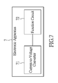
- FIG. 7 is a block diagram of an electronic apparatus according to an exemplary embodiment of the present disclosure.
- the electronic apparatus 7 comprises a current-to-voltage converter 71 and a function circuit 72 , wherein the current-to-voltage converter 71 is connected to the function circuit 72 , and the current-to-voltage converter 71 can be one of the current-to-voltage converters in the exemplary embodiments of the present disclosure or the modification.
- the current-to-voltage converter 71 is used to receive the current Iin, and output the voltage Vout to the function circuit 72 accordingly.
- the function circuit can execute the corresponding function according to the received voltage Vout.
- the electronic apparatus 7 is for example the touch control device, and the function circuit 72 is for example the touch control sensing circuit. However, it is noted that the number and the type of the above function circuit 72 are corresponding to the type of the electronic apparatus 7 , and the type of the electronic apparatus is not used to limit the present disclosure.
- he current-to-voltage converter provided by the exemplary embodiment of the present disclosure can have the high input range and wide output swing by using the current tracking bias circuit and the voltage clamp bias circuit.
- the current-to-voltage unit of the current-to-voltage converter can have the current control device to enhance the rising or falling speed of the output voltage of the current-to-voltage converter.
- the voltage clamp bias circuit can further maintains the drain-source voltage of the transistor in the current-to-voltage unit with a constant voltage value, so as to reduce the effect which the channel length modulation effect of the transistor affects the output voltage of the current-to-voltage converter.
Landscapes
- Engineering & Computer Science (AREA)
- Power Engineering (AREA)
- Amplifiers (AREA)
Abstract
Description
Claims (8)
Applications Claiming Priority (3)
| Application Number | Priority Date | Filing Date | Title |
|---|---|---|---|
| TW102116855 | 2013-05-13 | ||
| TW102116855A TWI502306B (en) | 2013-05-13 | 2013-05-13 | Current-to-voltage converter and electronic apparatus thereof |
| TW102116855A | 2013-05-13 |
Publications (2)
| Publication Number | Publication Date |
|---|---|
| US20140333348A1 US20140333348A1 (en) | 2014-11-13 |
| US9024664B2 true US9024664B2 (en) | 2015-05-05 |
Family
ID=51864345
Family Applications (1)
| Application Number | Title | Priority Date | Filing Date |
|---|---|---|---|
| US14/018,457 Active US9024664B2 (en) | 2013-05-13 | 2013-09-05 | Current-to-voltage converter and electronic apparatus thereof |
Country Status (2)
| Country | Link |
|---|---|
| US (1) | US9024664B2 (en) |
| TW (1) | TWI502306B (en) |
Families Citing this family (4)
| Publication number | Priority date | Publication date | Assignee | Title |
|---|---|---|---|---|
| CN105337616B (en) * | 2015-12-04 | 2018-11-20 | 上海兆芯集成电路有限公司 | Digital to Analog Converter and high pressure Circuit with tolerance |
| JP6324638B2 (en) * | 2015-12-21 | 2018-05-16 | 三菱電機株式会社 | Optical receiver, optical termination device, and optical communication system |
| KR102496317B1 (en) * | 2016-02-12 | 2023-02-06 | 주식회사 디비하이텍 | Sensing circuit and touch sensor including the same |
| US10811961B1 (en) * | 2019-09-09 | 2020-10-20 | Allegro Microsystems, Llc | Top-off charge pump and methods of operating same |
Citations (2)
| Publication number | Priority date | Publication date | Assignee | Title |
|---|---|---|---|---|
| US20070247533A1 (en) * | 2002-05-30 | 2007-10-25 | Sony Corporation | DC level control method, clamp circuit, and imaging apparatus |
| US20110169552A1 (en) * | 2008-09-05 | 2011-07-14 | Chun-Seok Jeong | On die thermal sensor suitable for auto self refresh, integrated circuit with the same and method for on die thermal sensor suitable for auto self refresh |
Family Cites Families (6)
| Publication number | Priority date | Publication date | Assignee | Title |
|---|---|---|---|---|
| JP4248773B2 (en) * | 2001-07-26 | 2009-04-02 | 富士通マイクロエレクトロニクス株式会社 | Current-voltage converter |
| US6707280B1 (en) * | 2002-09-09 | 2004-03-16 | Arques Technology, Inc. | Bidirectional voltage regulator sourcing and sinking current for line termination |
| US7012416B2 (en) * | 2003-12-09 | 2006-03-14 | Analog Devices, Inc. | Bandgap voltage reference |
| JP4823604B2 (en) * | 2005-08-05 | 2011-11-24 | ローム株式会社 | Soft start circuit, power supply, electrical equipment |
| JP2008011001A (en) * | 2006-06-28 | 2008-01-17 | Nec Electronics Corp | Current/voltage conversion circuit and conversion method |
| TWI437406B (en) * | 2010-10-25 | 2014-05-11 | Novatek Microelectronics Corp | Low noise current buffer circuit and i-v converter |
-
2013
- 2013-05-13 TW TW102116855A patent/TWI502306B/en active
- 2013-09-05 US US14/018,457 patent/US9024664B2/en active Active
Patent Citations (2)
| Publication number | Priority date | Publication date | Assignee | Title |
|---|---|---|---|---|
| US20070247533A1 (en) * | 2002-05-30 | 2007-10-25 | Sony Corporation | DC level control method, clamp circuit, and imaging apparatus |
| US20110169552A1 (en) * | 2008-09-05 | 2011-07-14 | Chun-Seok Jeong | On die thermal sensor suitable for auto self refresh, integrated circuit with the same and method for on die thermal sensor suitable for auto self refresh |
Also Published As
| Publication number | Publication date |
|---|---|
| TWI502306B (en) | 2015-10-01 |
| TW201443606A (en) | 2014-11-16 |
| US20140333348A1 (en) | 2014-11-13 |
Similar Documents
| Publication | Publication Date | Title |
|---|---|---|
| CN108370238B (en) | Optical receiver, optical terminal device and optical communication system | |
| WO2016082420A1 (en) | Low dropout linear voltage regulator | |
| US10128821B2 (en) | Low output impedance, high speed and high voltage generator for use in driving a capacitive load | |
| US9323264B2 (en) | Voltage regulator apparatus with sensing modules and related operating method thereof | |
| CN107024958B (en) | A kind of linear voltage-stabilizing circuit with fast load transient response | |
| CN115113682B (en) | Input reference voltage adjustment circuit | |
| US9024664B2 (en) | Current-to-voltage converter and electronic apparatus thereof | |
| US8836427B2 (en) | Folded cascode operational amplifier | |
| WO2016078618A1 (en) | Power control method, device and communication terminal for radio frequency power amplifier | |
| JP2017184122A (en) | Differential amplifier | |
| US10141897B2 (en) | Source follower | |
| US9543905B2 (en) | Amplifier circuit | |
| CN104038041B (en) | A kind of soft start circuit of switch power supply for ambipolar error amplifier | |
| TWI463792B (en) | Amplifier circuit with overshoot suppression | |
| CN103592990B (en) | A linear stabilized power supply and its voltage adjustment method | |
| US20130222036A1 (en) | Voltage level converting circuit | |
| US9467108B2 (en) | Operational amplifier circuit and method for enhancing driving capacity thereof | |
| JP2019527981A (en) | Selectable current limiter circuit | |
| US20130181777A1 (en) | Voltage regulator | |
| US20250379573A1 (en) | Leakage compensation circuit, chip, and electronic device | |
| CN109150188B (en) | A current mode digital-to-analog converter output stage circuit with adjustable output common mode level | |
| US11381225B1 (en) | Single ended receiver | |
| US20130257484A1 (en) | Voltage-to-current converter | |
| US11199591B2 (en) | Current detection circuit | |
| US10476447B2 (en) | Source follower |
Legal Events
| Date | Code | Title | Description |
|---|---|---|---|
| AS | Assignment |
Owner name: ILI TECHNOLOGY CORP., TAIWAN Free format text: ASSIGNMENT OF ASSIGNORS INTEREST;ASSIGNORS:CHENG, CHIH-JEN;HSU, CHENG-CHUNG;REEL/FRAME:031139/0289 Effective date: 20130813 |
|
| STCF | Information on status: patent grant |
Free format text: PATENTED CASE |
|
| AS | Assignment |
Owner name: MRISE TECHNOLOGY INC., TAIWAN Free format text: MERGER;ASSIGNOR:ILI TECHNOLOGY CORP.;REEL/FRAME:040688/0263 Effective date: 20150826 |
|
| AS | Assignment |
Owner name: ILI TECHNOLOGY CORP., TAIWAN Free format text: CHANGE OF NAME;ASSIGNOR:MRISE TECHNOLOGY INC.;REEL/FRAME:040676/0700 Effective date: 20161220 |
|
| MAFP | Maintenance fee payment |
Free format text: PAYMENT OF MAINTENANCE FEE, 4TH YEAR, LARGE ENTITY (ORIGINAL EVENT CODE: M1551); ENTITY STATUS OF PATENT OWNER: LARGE ENTITY Year of fee payment: 4 |
|
| AS | Assignment |
Owner name: ILI TECHNOLOGY HOLDING CORPORATION, CAYMAN ISLANDS Free format text: ASSIGNMENT OF ASSIGNORS INTEREST;ASSIGNOR:ILI TECHNOLOGY CORP.;REEL/FRAME:055257/0614 Effective date: 20201210 |
|
| AS | Assignment |
Owner name: ILI TECHNOLOGY CORP., TAIWAN Free format text: ASSIGNMENT OF ASSIGNORS INTEREST;ASSIGNOR:ILI TECHNOLOGY HOLDING CORPORATION;REEL/FRAME:060262/0911 Effective date: 20220322 |
|
| MAFP | Maintenance fee payment |
Free format text: PAYMENT OF MAINTENANCE FEE, 8TH YEAR, LARGE ENTITY (ORIGINAL EVENT CODE: M1552); ENTITY STATUS OF PATENT OWNER: LARGE ENTITY Year of fee payment: 8 |