US9005779B2 - Compound comprising a five-membered hetero ring, an organic electrical element using the same and a terminal thereof - Google Patents
Compound comprising a five-membered hetero ring, an organic electrical element using the same and a terminal thereof Download PDFInfo
- Publication number
- US9005779B2 US9005779B2 US13/699,040 US201113699040A US9005779B2 US 9005779 B2 US9005779 B2 US 9005779B2 US 201113699040 A US201113699040 A US 201113699040A US 9005779 B2 US9005779 B2 US 9005779B2
- Authority
- US
- United States
- Prior art keywords
- unsubstituted
- substituted
- organic
- group
- compound
- Prior art date
- Legal status (The legal status is an assumption and is not a legal conclusion. Google has not performed a legal analysis and makes no representation as to the accuracy of the status listed.)
- Active, expires
Links
- 0 C.C.C.C[Y]C.[1*]C1=C([2*])C([3*])=C([4*])C2=C1CC1=C2C([5*])=C([6*])C2=C1C1=C(/C=C\C=C/1)N2[Ar] Chemical compound C.C.C.C[Y]C.[1*]C1=C([2*])C([3*])=C([4*])C2=C1CC1=C2C([5*])=C([6*])C2=C1C1=C(/C=C\C=C/1)N2[Ar] 0.000 description 11
- VIZUPBYFLORCRA-UHFFFAOYSA-N C1=CC2=C(C=C1)C=C(C1=C3C=CC=CC3=C(C3=CC4=C(C=CC=C4)C=C3)C3=C1C=CC=C3)C=C2 Chemical compound C1=CC2=C(C=C1)C=C(C1=C3C=CC=CC3=C(C3=CC4=C(C=CC=C4)C=C3)C3=C1C=CC=C3)C=C2 VIZUPBYFLORCRA-UHFFFAOYSA-N 0.000 description 2
- ZKVYQAPWRGJOLZ-UHFFFAOYSA-N C1=CC=C(C2=CC=C(N(C3=C/C4=C(\C=C/3)C3=C(C=CC5=C3SC3=C5C=CC=C3)N4C3=CC=CC=C3)C3=C/C=C4/SC5=C(C=CC=C5)/C4=C\3)C=C2)C=C1.C1=CC=C(N2C3=C(C4=C2/C=C(N(C2=C/C=C5\SC6=C(C=CC=C6)\C5=C\2)C2=C/C5=C(\C=C/2)SC2=C5C=CC=C2)\C=C/4)C2=C(C=C3)C3=C(C=CC=C3)S2)C=C1.C1=CC=C(N2C3=C(C4=C2/C=C(N(C2=C5C=CC=CC5=CC=C2)C2=C/C=C5/SC6=C(C=CC=C6)/C5=C\2)\C=C/4)C2=C(C=C3)C3=C(C=CC=C3)S2)C=C1.C1=CC=C(N2C3=C(C4=C2/C=C(N(C2=CC5=C(C=CC=C5)C=C2)C2=C/C=C5/SC6=C(C=CC=C6)/C5=C\2)\C=C/4)C2=C(C=C3)C3=C(C=CC=C3)S2)C=C1 Chemical compound C1=CC=C(C2=CC=C(N(C3=C/C4=C(\C=C/3)C3=C(C=CC5=C3SC3=C5C=CC=C3)N4C3=CC=CC=C3)C3=C/C=C4/SC5=C(C=CC=C5)/C4=C\3)C=C2)C=C1.C1=CC=C(N2C3=C(C4=C2/C=C(N(C2=C/C=C5\SC6=C(C=CC=C6)\C5=C\2)C2=C/C5=C(\C=C/2)SC2=C5C=CC=C2)\C=C/4)C2=C(C=C3)C3=C(C=CC=C3)S2)C=C1.C1=CC=C(N2C3=C(C4=C2/C=C(N(C2=C5C=CC=CC5=CC=C2)C2=C/C=C5/SC6=C(C=CC=C6)/C5=C\2)\C=C/4)C2=C(C=C3)C3=C(C=CC=C3)S2)C=C1.C1=CC=C(N2C3=C(C4=C2/C=C(N(C2=CC5=C(C=CC=C5)C=C2)C2=C/C=C5/SC6=C(C=CC=C6)/C5=C\2)\C=C/4)C2=C(C=C3)C3=C(C=CC=C3)S2)C=C1 ZKVYQAPWRGJOLZ-UHFFFAOYSA-N 0.000 description 2
- UKOFRRIUWWVRQX-UHFFFAOYSA-N C1=CC=C(C2=CC=C(N(C3=C/C=C4C(=C/3)/C3=C(C=CC=C3)N/4C3=CC=CC=C3)C3=C/C4=C(\C=C/3)C3=C(C=CC5=C3SC3=C5C=CC=C3)N4C3=CC=CC=C3)C=C2)C=C1.C1=CC=C(N2C3=C(C=CC=C3)C3=C2/C=C\C(N(C2=C/C=C4C(=C/2)/C2=C(C=CC=C2)N/4C2=CC=CC=C2)C2=C/C4=C(\C=C/2)C2=C(C=CC5=C2SC2=C5C=CC=C2)N4C2=CC=CC=C2)=C/3)C=C1.CC1(C)C2=C(C=CC=C2)C2=C\C=C(N(C3=C/C4=C(\C=C/3)SC3=C4C=CC=C3)C3=C/C4=C(\C=C/3)C3=C(C=CC5=C3SC3=C5C=CC=C3)N4C3=CC=CC=C3)/C=C\21 Chemical compound C1=CC=C(C2=CC=C(N(C3=C/C=C4C(=C/3)/C3=C(C=CC=C3)N/4C3=CC=CC=C3)C3=C/C4=C(\C=C/3)C3=C(C=CC5=C3SC3=C5C=CC=C3)N4C3=CC=CC=C3)C=C2)C=C1.C1=CC=C(N2C3=C(C=CC=C3)C3=C2/C=C\C(N(C2=C/C=C4C(=C/2)/C2=C(C=CC=C2)N/4C2=CC=CC=C2)C2=C/C4=C(\C=C/2)C2=C(C=CC5=C2SC2=C5C=CC=C2)N4C2=CC=CC=C2)=C/3)C=C1.CC1(C)C2=C(C=CC=C2)C2=C\C=C(N(C3=C/C4=C(\C=C/3)SC3=C4C=CC=C3)C3=C/C4=C(\C=C/3)C3=C(C=CC5=C3SC3=C5C=CC=C3)N4C3=CC=CC=C3)/C=C\21 UKOFRRIUWWVRQX-UHFFFAOYSA-N 0.000 description 2
- DAQCGDVABHPXDR-UHFFFAOYSA-N C1=CC=C(C2=CC=C(N(C3=C4C=CC=CC4=CC=C3)C3=C/C4=C(\C=C/3)C3=C(C=CC5=C3SC3=C5C=CC=C3)N4C3=CC=CC=C3)C=C2)C=C1.C1=CC=C(N2C3=C(C4=C2/C=C(N(C2=CC=C5C=CC=CC5=C2)C2=C5C=CC=CC5=CC=C2)\C=C/4)C2=C(C=C3)C3=C(C=CC=C3)S2)C=C1.C1=CC=C(N2C3=C(C4=C2/C=C(N(C2=CC=C5C=CC=CC5=C2)C2=CC5=C(C=CC=C5)C=C2)\C=C/4)C2=C(C=C3)C3=C(C=CC=C3)S2)C=C1.C1=CC=C(N2C3=C(C4=C2/C=C(N(C2=CC=CC5=C2C=CC=C5)C2=CC=CC5=C2C=CC=C5)\C=C/4)C2=C(C=C3)C3=C(C=CC=C3)S2)C=C1 Chemical compound C1=CC=C(C2=CC=C(N(C3=C4C=CC=CC4=CC=C3)C3=C/C4=C(\C=C/3)C3=C(C=CC5=C3SC3=C5C=CC=C3)N4C3=CC=CC=C3)C=C2)C=C1.C1=CC=C(N2C3=C(C4=C2/C=C(N(C2=CC=C5C=CC=CC5=C2)C2=C5C=CC=CC5=CC=C2)\C=C/4)C2=C(C=C3)C3=C(C=CC=C3)S2)C=C1.C1=CC=C(N2C3=C(C4=C2/C=C(N(C2=CC=C5C=CC=CC5=C2)C2=CC5=C(C=CC=C5)C=C2)\C=C/4)C2=C(C=C3)C3=C(C=CC=C3)S2)C=C1.C1=CC=C(N2C3=C(C4=C2/C=C(N(C2=CC=CC5=C2C=CC=C5)C2=CC=CC5=C2C=CC=C5)\C=C/4)C2=C(C=C3)C3=C(C=CC=C3)S2)C=C1 DAQCGDVABHPXDR-UHFFFAOYSA-N 0.000 description 2
- SWUVVHPXDGFIRG-UHFFFAOYSA-N C1=CC=C(C2=CC=C(N(C3=C4C=CC=CC4=CC=C3)C3=C/C4=C(\C=C/3)N(C3=CC=CC=C3)C3=C4C4=C(C=C3)C3=C(C=CC=C3)S4)C=C2)C=C1.C1=CC=C(N2C3=C(C4=C2/C=C\C(N(C2=C5C=CC=CC5=CC=C2)C2=C5C=CC=CC5=CC=C2)=C/4)C2=C(C=C3)C3=C(C=CC=C3)S2)C=C1.C1=CC=C(N2C3=C(C4=C2/C=C\C(N(C2=CC5=C(C=CC=C5)C=C2)C2=C5C=CC=CC5=CC=C2)=C/4)C2=C(C=C3)C3=C(C=CC=C3)S2)C=C1.C1=CC=C(N2C3=C(C4=C2/C=C\C(N(C2=CC5=C(C=CC=C5)C=C2)C2=CC5=C(C=CC=C5)C=C2)=C/4)C2=C(C=C3)C3=C(C=CC=C3)S2)C=C1 Chemical compound C1=CC=C(C2=CC=C(N(C3=C4C=CC=CC4=CC=C3)C3=C/C4=C(\C=C/3)N(C3=CC=CC=C3)C3=C4C4=C(C=C3)C3=C(C=CC=C3)S4)C=C2)C=C1.C1=CC=C(N2C3=C(C4=C2/C=C\C(N(C2=C5C=CC=CC5=CC=C2)C2=C5C=CC=CC5=CC=C2)=C/4)C2=C(C=C3)C3=C(C=CC=C3)S2)C=C1.C1=CC=C(N2C3=C(C4=C2/C=C\C(N(C2=CC5=C(C=CC=C5)C=C2)C2=C5C=CC=CC5=CC=C2)=C/4)C2=C(C=C3)C3=C(C=CC=C3)S2)C=C1.C1=CC=C(N2C3=C(C4=C2/C=C\C(N(C2=CC5=C(C=CC=C5)C=C2)C2=CC5=C(C=CC=C5)C=C2)=C/4)C2=C(C=C3)C3=C(C=CC=C3)S2)C=C1 SWUVVHPXDGFIRG-UHFFFAOYSA-N 0.000 description 2
- HHXKUVRWWGCXNU-UHFFFAOYSA-N C1=CC=C(C2=CC=C(N(C3=CC(C4=C/C5=C(\C=C/4)C4=C(C=CC6=C4SC4=C6C=CC=C4)N5C4=CC=CC=C4)=CC(N(C4=CC=C(C5=CC=CC=C5)C=C4)C4=C/C5=C(\C=C/4)SC4=C5C=CC=C4)=C3)C3=C\C=C4\SC5=C(C=CC=C5)\C4=C\3)C=C2)C=C1.C1=CC=C(N2C3=C(C4=C2/C=C(C2=CC(N(C5=C/C6=C(\C=C/5)SC5=C6C=CC=C5)C5=C/C6=C(\C=C/5)SC5=C6C=CC=C5)=CC(N(C5=C/C=C6\SC7=C(C=CC=C7)\C6=C\5)C5=C/C6=C(\C=C/5)SC5=C6C=CC=C5)=C2)\C=C/4)C2=C(C=C3)C3=C(C=CC=C3)S2)C=C1.C1=CC=C(N2C3=C(C4=C2/C=C(C2=CC(N(C5=CC=C6C=CC=CC6=C5)C5=C/C6=C(\C=C/5)SC5=C6C=CC=C5)=CC(N(C5=CC6=C(C=CC=C6)C=C5)C5=C\C=C6\SC7=C(C=CC=C7)\C6=C\5)=C2)\C=C/4)C2=C(C=C3)C3=C(C=CC=C3)S2)C=C1 Chemical compound C1=CC=C(C2=CC=C(N(C3=CC(C4=C/C5=C(\C=C/4)C4=C(C=CC6=C4SC4=C6C=CC=C4)N5C4=CC=CC=C4)=CC(N(C4=CC=C(C5=CC=CC=C5)C=C4)C4=C/C5=C(\C=C/4)SC4=C5C=CC=C4)=C3)C3=C\C=C4\SC5=C(C=CC=C5)\C4=C\3)C=C2)C=C1.C1=CC=C(N2C3=C(C4=C2/C=C(C2=CC(N(C5=C/C6=C(\C=C/5)SC5=C6C=CC=C5)C5=C/C6=C(\C=C/5)SC5=C6C=CC=C5)=CC(N(C5=C/C=C6\SC7=C(C=CC=C7)\C6=C\5)C5=C/C6=C(\C=C/5)SC5=C6C=CC=C5)=C2)\C=C/4)C2=C(C=C3)C3=C(C=CC=C3)S2)C=C1.C1=CC=C(N2C3=C(C4=C2/C=C(C2=CC(N(C5=CC=C6C=CC=CC6=C5)C5=C/C6=C(\C=C/5)SC5=C6C=CC=C5)=CC(N(C5=CC6=C(C=CC=C6)C=C5)C5=C\C=C6\SC7=C(C=CC=C7)\C6=C\5)=C2)\C=C/4)C2=C(C=C3)C3=C(C=CC=C3)S2)C=C1 HHXKUVRWWGCXNU-UHFFFAOYSA-N 0.000 description 2
- AXRCVQDVQWWXTH-UHFFFAOYSA-N C1=CC=C(C2=CC=C(N(C3=CC(N(C4=CC=C(C5=CC=CC=C5)C=C4)C4=C/C=C5/SC6=C(C=CC=C6)/C5=C\4)=CC(C4=C/C5=C(\C=C/4)N(C4=CC=CC=C4)C4=C5C5=C(C=C4)C4=C(C=CC=C4)S5)=C3)C3=C/C4=C(\C=C/3)SC3=C4C=CC=C3)C=C2)C=C1.C1=CC=C(N2C3=C(C4=C2/C=C\C(C2=CC(N(C5=CC=C6C=CC=CC6=C5)C5=C/C6=C(\C=C/5)SC5=C6C=CC=C5)=CC(N(C5=CC6=C(C=CC=C6)C=C5)C5=C/C=C6/SC7=C(C=CC=C7)/C6=C\5)=C2)=C/4)C2=C(C=C3)C3=C(C=CC=C3)S2)C=C1.C1=CC=C(N2C3=C(C4=C2/C=C\C(C2=CC(N(C5=CC=CC6=C5C=CC=C6)C5=C/C6=C(\C=C/5)SC5=C6C=CC=C5)=CC(N(C5=C6C=CC=CC6=CC=C5)C5=C/C=C6/SC7=C(C=CC=C7)/C6=C\5)=C2)=C/4)C2=C(C=C3)C3=C(C=CC=C3)S2)C=C1 Chemical compound C1=CC=C(C2=CC=C(N(C3=CC(N(C4=CC=C(C5=CC=CC=C5)C=C4)C4=C/C=C5/SC6=C(C=CC=C6)/C5=C\4)=CC(C4=C/C5=C(\C=C/4)N(C4=CC=CC=C4)C4=C5C5=C(C=C4)C4=C(C=CC=C4)S5)=C3)C3=C/C4=C(\C=C/3)SC3=C4C=CC=C3)C=C2)C=C1.C1=CC=C(N2C3=C(C4=C2/C=C\C(C2=CC(N(C5=CC=C6C=CC=CC6=C5)C5=C/C6=C(\C=C/5)SC5=C6C=CC=C5)=CC(N(C5=CC6=C(C=CC=C6)C=C5)C5=C/C=C6/SC7=C(C=CC=C7)/C6=C\5)=C2)=C/4)C2=C(C=C3)C3=C(C=CC=C3)S2)C=C1.C1=CC=C(N2C3=C(C4=C2/C=C\C(C2=CC(N(C5=CC=CC6=C5C=CC=C6)C5=C/C6=C(\C=C/5)SC5=C6C=CC=C5)=CC(N(C5=C6C=CC=CC6=CC=C5)C5=C/C=C6/SC7=C(C=CC=C7)/C6=C\5)=C2)=C/4)C2=C(C=C3)C3=C(C=CC=C3)S2)C=C1 AXRCVQDVQWWXTH-UHFFFAOYSA-N 0.000 description 2
- MCCRQWYOKZSUFI-UHFFFAOYSA-N C1=CC=C(C2=CC=C(N(C3=CC(N(C4=CC=C(C5=CC=CC=C5)C=C4)C4=C/C=C5C(=C/4)/C4=C(C=CC=C4)N/5C4=CC=CC=C4)=CC(C4=C/C5=C(\C=C/4)C4=C(C=CC6=C4SC4=C6C=CC=C4)N5C4=CC=CC=C4)=C3)C3=CC4=C(C=C3)N(C3=CC=CC=C3)C3=C4C=CC=C3)C=C2)C=C1.C1=CC=C(N2C3=C(C=CC=C3)C3=C2C=CC(N(C2=CC(N(C4=C/C=C5C(=C/4)/C4=C(C=CC=C4)N/5C4=CC=CC=C4)C4=C/C5=C(\C=C/4)N(C4=CC=CC=C4)C4=C5C=CC=C4)=CC(C4=C/C5=C(\C=C/4)C4=C(C=CC6=C4SC4=C6C=CC=C4)N5C4=CC=CC=C4)=C2)C2=C/C=C4C(=C/2)\C2=C(C=CC=C2)N\4C2=CC=CC=C2)=C3)C=C1 Chemical compound C1=CC=C(C2=CC=C(N(C3=CC(N(C4=CC=C(C5=CC=CC=C5)C=C4)C4=C/C=C5C(=C/4)/C4=C(C=CC=C4)N/5C4=CC=CC=C4)=CC(C4=C/C5=C(\C=C/4)C4=C(C=CC6=C4SC4=C6C=CC=C4)N5C4=CC=CC=C4)=C3)C3=CC4=C(C=C3)N(C3=CC=CC=C3)C3=C4C=CC=C3)C=C2)C=C1.C1=CC=C(N2C3=C(C=CC=C3)C3=C2C=CC(N(C2=CC(N(C4=C/C=C5C(=C/4)/C4=C(C=CC=C4)N/5C4=CC=CC=C4)C4=C/C5=C(\C=C/4)N(C4=CC=CC=C4)C4=C5C=CC=C4)=CC(C4=C/C5=C(\C=C/4)C4=C(C=CC6=C4SC4=C6C=CC=C4)N5C4=CC=CC=C4)=C2)C2=C/C=C4C(=C/2)\C2=C(C=CC=C2)N\4C2=CC=CC=C2)=C3)C=C1 MCCRQWYOKZSUFI-UHFFFAOYSA-N 0.000 description 2
- BUZWTKDOUOYYRR-UHFFFAOYSA-N C1=CC=C(C2=CC=C(N(C3=CC(N(C4=CC=C(C5=CC=CC=C5)C=C4)C4=C/C=C5C(=C/4)\C4=C(C=CC=C4)N\5C4=CC=CC=C4)=CC(C4=C/C5=C(\C=C/4)N(C4=CC=CC=C4)C4=C5C5=C(C=C4)C4=C(C=CC=C4)S5)=C3)C3=C/C4=C(\C=C/3)N(C3=CC=CC=C3)C3=C4C=CC=C3)C=C2)C=C1.C1=CC=C(N2C3=C(C=CC=C3)C3=C2/C=C\C(N(C2=CC(C4=C/C5=C(\C=C/4)N(C4=CC=CC=C4)C4=C5C5=C(C=C4)C4=C(C=CC=C4)S5)=CC(N(C4=C/C5=C(\C=C/4)N(C4=CC=CC=C4)C4=C5C=CC=C4)C4=C/C=C5C(=C/4)\C4=C(C=CC=C4)N\5C4=CC=CC=C4)=C2)C2=C/C=C4C(=C/2)/C2=C(C=CC=C2)N/4C2=CC=CC=C2)=C/3)C=C1.C1=CC=C(N2C3=C(C=CC=C3)C3=C2/C=C\C(N(C2=CC=C4C=CC=CC4=C2)C2=CC(N(C4=CC5=C(C=CC=C5)C=C4)C4=C/C=C5C(=C/4)\C4=C(C=CC=C4)N\5C4=CC=CC=C4)=CC(C4=C/C5=C(\C=C/4)N(C4=CC=CC=C4)C4=C5C5=C(C=C4)C4=C(C=CC=C4)S5)=C2)=C/3)C=C1 Chemical compound C1=CC=C(C2=CC=C(N(C3=CC(N(C4=CC=C(C5=CC=CC=C5)C=C4)C4=C/C=C5C(=C/4)\C4=C(C=CC=C4)N\5C4=CC=CC=C4)=CC(C4=C/C5=C(\C=C/4)N(C4=CC=CC=C4)C4=C5C5=C(C=C4)C4=C(C=CC=C4)S5)=C3)C3=C/C4=C(\C=C/3)N(C3=CC=CC=C3)C3=C4C=CC=C3)C=C2)C=C1.C1=CC=C(N2C3=C(C=CC=C3)C3=C2/C=C\C(N(C2=CC(C4=C/C5=C(\C=C/4)N(C4=CC=CC=C4)C4=C5C5=C(C=C4)C4=C(C=CC=C4)S5)=CC(N(C4=C/C5=C(\C=C/4)N(C4=CC=CC=C4)C4=C5C=CC=C4)C4=C/C=C5C(=C/4)\C4=C(C=CC=C4)N\5C4=CC=CC=C4)=C2)C2=C/C=C4C(=C/2)/C2=C(C=CC=C2)N/4C2=CC=CC=C2)=C/3)C=C1.C1=CC=C(N2C3=C(C=CC=C3)C3=C2/C=C\C(N(C2=CC=C4C=CC=CC4=C2)C2=CC(N(C4=CC5=C(C=CC=C5)C=C4)C4=C/C=C5C(=C/4)\C4=C(C=CC=C4)N\5C4=CC=CC=C4)=CC(C4=C/C5=C(\C=C/4)N(C4=CC=CC=C4)C4=C5C5=C(C=C4)C4=C(C=CC=C4)S5)=C2)=C/3)C=C1 BUZWTKDOUOYYRR-UHFFFAOYSA-N 0.000 description 2
- JLCUJWATWDAETK-UHFFFAOYSA-N C1=CC=C(C2=CC=C(N(C3=CC(N(C4=CC=C(C5=CC=CC=C5)C=C4)C4=C5C=CC=CC5=CC=C4)=CC(C4=C/C5=C(\C=C/4)C4=C(C=CC6=C4SC4=C6C=CC=C4)N5C4=CC=CC=C4)=C3)C3=CC=CC4=C3C=CC=C4)C=C2)C=C1.C1=CC=C(C2=CC=C(N(C3=CC=C(C4=CC=CC=C4)C=C3)C3=CC(C4=C/C5=C(\C=C/4)C4=C(C=CC6=C4SC4=C6C=CC=C4)N5C4=CC=CC=C4)=CC(N(C4=CC=C(C5=CC=CC=C5)C=C4)C4=CC=C(C5=CC=CC=C5)C=C4)=C3)C=C2)C=C1.C1=CC=C(C2=CC=C(N(C3=CC=C4C=CC=CC4=C3)C3=CC(N(C4=CC=C(C5=CC=CC=C5)C=C4)C4=CC5=C(C=CC=C5)C=C4)=CC(C4=C/C5=C(\C=C/4)C4=C(C=CC6=C4SC4=C6C=CC=C4)N5C4=CC=CC=C4)=C3)C=C2)C=C1 Chemical compound C1=CC=C(C2=CC=C(N(C3=CC(N(C4=CC=C(C5=CC=CC=C5)C=C4)C4=C5C=CC=CC5=CC=C4)=CC(C4=C/C5=C(\C=C/4)C4=C(C=CC6=C4SC4=C6C=CC=C4)N5C4=CC=CC=C4)=C3)C3=CC=CC4=C3C=CC=C4)C=C2)C=C1.C1=CC=C(C2=CC=C(N(C3=CC=C(C4=CC=CC=C4)C=C3)C3=CC(C4=C/C5=C(\C=C/4)C4=C(C=CC6=C4SC4=C6C=CC=C4)N5C4=CC=CC=C4)=CC(N(C4=CC=C(C5=CC=CC=C5)C=C4)C4=CC=C(C5=CC=CC=C5)C=C4)=C3)C=C2)C=C1.C1=CC=C(C2=CC=C(N(C3=CC=C4C=CC=CC4=C3)C3=CC(N(C4=CC=C(C5=CC=CC=C5)C=C4)C4=CC5=C(C=CC=C5)C=C4)=CC(C4=C/C5=C(\C=C/4)C4=C(C=CC6=C4SC4=C6C=CC=C4)N5C4=CC=CC=C4)=C3)C=C2)C=C1 JLCUJWATWDAETK-UHFFFAOYSA-N 0.000 description 2
- DSUUYPWVFKQNSE-UHFFFAOYSA-N C1=CC=C(C2=CC=C(N(C3=CC(N(C4=CC=C(C5=CC=CC=C5)C=C4)C4=C5C=CC=CC5=CC=C4)=CC(C4=C/C5=C(\C=C/4)N(C4=CC=CC=C4)C4=C5C5=C(C=C4)C4=C(C=CC=C4)S5)=C3)C3=CC=CC4=C3C=CC=C4)C=C2)C=C1.C1=CC=C(C2=CC=C(N(C3=CC=C(C4=CC=CC=C4)C=C3)C3=CC(C4=C/C5=C(\C=C/4)N(C4=CC=CC=C4)C4=C5C5=C(C=C4)C4=C(C=CC=C4)S5)=CC(N(C4=CC=C(C5=CC=CC=C5)C=C4)C4=CC=C(C5=CC=CC=C5)C=C4)=C3)C=C2)C=C1.C1=CC=C(C2=CC=C(N(C3=CC=C4C=CC=CC4=C3)C3=CC(N(C4=CC=C(C5=CC=CC=C5)C=C4)C4=CC5=C(C=CC=C5)C=C4)=CC(C4=C/C5=C(\C=C/4)N(C4=CC=CC=C4)C4=C5C5=C(C=C4)C4=C(C=CC=C4)S5)=C3)C=C2)C=C1 Chemical compound C1=CC=C(C2=CC=C(N(C3=CC(N(C4=CC=C(C5=CC=CC=C5)C=C4)C4=C5C=CC=CC5=CC=C4)=CC(C4=C/C5=C(\C=C/4)N(C4=CC=CC=C4)C4=C5C5=C(C=C4)C4=C(C=CC=C4)S5)=C3)C3=CC=CC4=C3C=CC=C4)C=C2)C=C1.C1=CC=C(C2=CC=C(N(C3=CC=C(C4=CC=CC=C4)C=C3)C3=CC(C4=C/C5=C(\C=C/4)N(C4=CC=CC=C4)C4=C5C5=C(C=C4)C4=C(C=CC=C4)S5)=CC(N(C4=CC=C(C5=CC=CC=C5)C=C4)C4=CC=C(C5=CC=CC=C5)C=C4)=C3)C=C2)C=C1.C1=CC=C(C2=CC=C(N(C3=CC=C4C=CC=CC4=C3)C3=CC(N(C4=CC=C(C5=CC=CC=C5)C=C4)C4=CC5=C(C=CC=C5)C=C4)=CC(C4=C/C5=C(\C=C/4)N(C4=CC=CC=C4)C4=C5C5=C(C=C4)C4=C(C=CC=C4)S5)=C3)C=C2)C=C1 DSUUYPWVFKQNSE-UHFFFAOYSA-N 0.000 description 2
- DSTOVDFGYHXVDG-UHFFFAOYSA-N C1=CC=C(C2=CC=C(N(C3=CC4=C(C=C3)N(C3=CC=CC=C3)C3=C4C=CC=C3)C3=C/C4=C(\C=C/3)N(C3=CC=CC=C3)C3=C4C4=C(C=C3)C3=C(C=CC=C3)S4)C=C2)C=C1.C1=CC=C(N2C3=C(C=CC=C3)C3=C2C=CC(N(C2=C4C=CC=CC4=CC=C2)C2=C/C4=C(\C=C/2)N(C2=CC=CC=C2)C2=C4C4=C(C=C2)C2=C(C=CC=C2)S4)=C3)C=C1.C1=CC=C(N2C3=C(C=CC=C3)C3=C2C=CC(N(C2=CC4=C(C=CC=C4)C=C2)C2=C/C4=C(\C=C/2)N(C2=CC=CC=C2)C2=C4C4=C(C=C2)C2=C(C=CC=C2)S4)=C3)C=C1 Chemical compound C1=CC=C(C2=CC=C(N(C3=CC4=C(C=C3)N(C3=CC=CC=C3)C3=C4C=CC=C3)C3=C/C4=C(\C=C/3)N(C3=CC=CC=C3)C3=C4C4=C(C=C3)C3=C(C=CC=C3)S4)C=C2)C=C1.C1=CC=C(N2C3=C(C=CC=C3)C3=C2C=CC(N(C2=C4C=CC=CC4=CC=C2)C2=C/C4=C(\C=C/2)N(C2=CC=CC=C2)C2=C4C4=C(C=C2)C2=C(C=CC=C2)S4)=C3)C=C1.C1=CC=C(N2C3=C(C=CC=C3)C3=C2C=CC(N(C2=CC4=C(C=CC=C4)C=C2)C2=C/C4=C(\C=C/2)N(C2=CC=CC=C2)C2=C4C4=C(C=C2)C2=C(C=CC=C2)S4)=C3)C=C1 DSTOVDFGYHXVDG-UHFFFAOYSA-N 0.000 description 2
- VQQFRSCZNPUTEZ-UHFFFAOYSA-N C1=CC=C(C2=CC=C(N(C3=CC4=C(C=C3)SC3=C4C=CC=C3)C3=C/C4=C(\C=C/3)N(C3=CC=CC=C3)C3=C4C4=C(C=C3)C3=C(C=CC=C3)S4)C=C2)C=C1.C1=CC=C(N2C3=C(C4=C2/C=C\C(N(C2=CC5=C(C=C2)SC2=C5C=CC=C2)C2=CC5=C(C=C2)SC2=C5C=CC=C2)=C/4)C2=C(C=C3)C3=C(C=CC=C3)S2)C=C1.C1=CC=C(N2C3=C(C=CC=C3)C3=C2C=CC(N(C2=CC=CC=C2)C2=C/C4=C(\C=C/2)N(C2=CC=CC=C2)C2=C4C4=C(C=C2)C2=C(C=CC=C2)S4)=C3)C=C1 Chemical compound C1=CC=C(C2=CC=C(N(C3=CC4=C(C=C3)SC3=C4C=CC=C3)C3=C/C4=C(\C=C/3)N(C3=CC=CC=C3)C3=C4C4=C(C=C3)C3=C(C=CC=C3)S4)C=C2)C=C1.C1=CC=C(N2C3=C(C4=C2/C=C\C(N(C2=CC5=C(C=C2)SC2=C5C=CC=C2)C2=CC5=C(C=C2)SC2=C5C=CC=C2)=C/4)C2=C(C=C3)C3=C(C=CC=C3)S2)C=C1.C1=CC=C(N2C3=C(C=CC=C3)C3=C2C=CC(N(C2=CC=CC=C2)C2=C/C4=C(\C=C/2)N(C2=CC=CC=C2)C2=C4C4=C(C=C2)C2=C(C=CC=C2)S4)=C3)C=C1 VQQFRSCZNPUTEZ-UHFFFAOYSA-N 0.000 description 2
- YFOPJHWJRCXVPQ-UHFFFAOYSA-N C1=CC=C(C2=CC=C(N(C3=CC4=C(C=CC=C4)C=C3)C3=C/C4=C(\C=C/3)C3=C(C=CC5=C3SC3=C5C=CC=C3)N4C3=CC=CC=C3)C=C2)C=C1.C1=CC=C(C2=CC=C(N(C3=CC=C(C4=CC=CC=C4)C=C3)C3=C/C4=C(\C=C/3)C3=C(C=CC5=C3SC3=C5C=CC=C3)N4C3=CC=CC=C3)C=C2)C=C1.CC1(C)C2=CC(N(C3=C4C=CC=CC4=CC=C3)C3=C/C4=C(\C=C/3)C3=C(C=CC5=C3SC3=C5C=CC=C3)N4C3=CC=CC=C3)=CC=C2C2=C1C=CC=C2.CC1(C)C2=CC(N(C3=CC=CC=C3)C3=C/C4=C(\C=C/3)C3=C(C=CC5=C3SC3=C5C=CC=C3)N4C3=CC=CC=C3)=CC=C2C2=C1C=CC=C2 Chemical compound C1=CC=C(C2=CC=C(N(C3=CC4=C(C=CC=C4)C=C3)C3=C/C4=C(\C=C/3)C3=C(C=CC5=C3SC3=C5C=CC=C3)N4C3=CC=CC=C3)C=C2)C=C1.C1=CC=C(C2=CC=C(N(C3=CC=C(C4=CC=CC=C4)C=C3)C3=C/C4=C(\C=C/3)C3=C(C=CC5=C3SC3=C5C=CC=C3)N4C3=CC=CC=C3)C=C2)C=C1.CC1(C)C2=CC(N(C3=C4C=CC=CC4=CC=C3)C3=C/C4=C(\C=C/3)C3=C(C=CC5=C3SC3=C5C=CC=C3)N4C3=CC=CC=C3)=CC=C2C2=C1C=CC=C2.CC1(C)C2=CC(N(C3=CC=CC=C3)C3=C/C4=C(\C=C/3)C3=C(C=CC5=C3SC3=C5C=CC=C3)N4C3=CC=CC=C3)=CC=C2C2=C1C=CC=C2 YFOPJHWJRCXVPQ-UHFFFAOYSA-N 0.000 description 2
- RHSYDQRWTVXGPI-UHFFFAOYSA-N C1=CC=C(C2=CC=C(N(C3=CC4=C(C=CC=C4)C=C3)C3=C/C4=C(\C=C/3)N(C3=CC=CC=C3)C3=C4C4=C(C=C3)C3=C(C=CC=C3)S4)C=C2)C=C1.C1=CC=C(C2=CC=C(N(C3=CC=C(C4=CC=CC=C4)C=C3)C3=C/C4=C(\C=C/3)N(C3=CC=CC=C3)C3=C4C4=C(C=C3)C3=C(C=CC=C3)S4)C=C2)C=C1.CC1(C)C2=C(C=CC=C2)C2=C/C=C(N(C3=CC=CC=C3)C3=C/C4=C(\C=C/3)N(C3=CC=CC=C3)C3=C4C4=C(C=C3)C3=C(C=CC=C3)S4)/C=C\21 Chemical compound C1=CC=C(C2=CC=C(N(C3=CC4=C(C=CC=C4)C=C3)C3=C/C4=C(\C=C/3)N(C3=CC=CC=C3)C3=C4C4=C(C=C3)C3=C(C=CC=C3)S4)C=C2)C=C1.C1=CC=C(C2=CC=C(N(C3=CC=C(C4=CC=CC=C4)C=C3)C3=C/C4=C(\C=C/3)N(C3=CC=CC=C3)C3=C4C4=C(C=C3)C3=C(C=CC=C3)S4)C=C2)C=C1.CC1(C)C2=C(C=CC=C2)C2=C/C=C(N(C3=CC=CC=C3)C3=C/C4=C(\C=C/3)N(C3=CC=CC=C3)C3=C4C4=C(C=C3)C3=C(C=CC=C3)S4)/C=C\21 RHSYDQRWTVXGPI-UHFFFAOYSA-N 0.000 description 2
- ILKYFZMYASGNNR-UHFFFAOYSA-N C1=CC=C(C2=CC=C(N(C3=CC=C(C4=C/C5=C(\C=C/4)C4=C(C=CC6=C4SC4=C6C=CC=C4)N5C4=CC=CC=C4)C=C3)C3=C/C=C4/SC5=C(C=CC=C5)/C4=C\3)C=C2)C=C1.C1=CC=C(N2C3=C(C4=C2/C=C(C2=CC=C(N(C5=C/C=C6\SC7=C(C=CC=C7)\C6=C\5)C5=C/C6=C(\C=C/5)SC5=C6C=CC=C5)C=C2)\C=C/4)C2=C(C=C3)C3=C(C=CC=C3)S2)C=C1.C1=CC=C(N2C3=C(C4=C2/C=C(C2=CC=C(N(C5=C6C=CC=CC6=CC=C5)C5=C/C=C6/SC7=C(C=CC=C7)/C6=C\5)C=C2)\C=C/4)C2=C(C=C3)C3=C(C=CC=C3)S2)C=C1.C1=CC=C(N2C3=C(C4=C2/C=C(C2=CC=C(N(C5=CC6=C(C=CC=C6)C=C5)C5=C/C=C6/SC7=C(C=CC=C7)/C6=C\5)C=C2)\C=C/4)C2=C(C=C3)C3=C(C=CC=C3)S2)C=C1 Chemical compound C1=CC=C(C2=CC=C(N(C3=CC=C(C4=C/C5=C(\C=C/4)C4=C(C=CC6=C4SC4=C6C=CC=C4)N5C4=CC=CC=C4)C=C3)C3=C/C=C4/SC5=C(C=CC=C5)/C4=C\3)C=C2)C=C1.C1=CC=C(N2C3=C(C4=C2/C=C(C2=CC=C(N(C5=C/C=C6\SC7=C(C=CC=C7)\C6=C\5)C5=C/C6=C(\C=C/5)SC5=C6C=CC=C5)C=C2)\C=C/4)C2=C(C=C3)C3=C(C=CC=C3)S2)C=C1.C1=CC=C(N2C3=C(C4=C2/C=C(C2=CC=C(N(C5=C6C=CC=CC6=CC=C5)C5=C/C=C6/SC7=C(C=CC=C7)/C6=C\5)C=C2)\C=C/4)C2=C(C=C3)C3=C(C=CC=C3)S2)C=C1.C1=CC=C(N2C3=C(C4=C2/C=C(C2=CC=C(N(C5=CC6=C(C=CC=C6)C=C5)C5=C/C=C6/SC7=C(C=CC=C7)/C6=C\5)C=C2)\C=C/4)C2=C(C=C3)C3=C(C=CC=C3)S2)C=C1 ILKYFZMYASGNNR-UHFFFAOYSA-N 0.000 description 2
- MGFGOJCJIHCJKW-UHFFFAOYSA-N C1=CC=C(C2=CC=C(N(C3=CC=C(C4=C/C5=C(\C=C/4)C4=C(C=CC6=C4SC4=C6C=CC=C4)N5C4=CC=CC=C4)C=C3)C3=C/C=C4C(=C/3)/C3=C(C=CC=C3)N/4C3=CC=CC=C3)C=C2)C=C1.C1=CC=C(N2C3=C(C=CC=C3)C3=C2/C=C\C(N(C2=CC=C(C4=C/C5=C(\C=C/4)C4=C(C=CC6=C4SC4=C6C=CC=C4)N5C4=CC=CC=C4)C=C2)C2=C/C=C4C(=C/2)/C2=C(C=CC=C2)N/4C2=CC=CC=C2)=C/3)C=C1.CC1(C)C2=C(C=CC=C2)C2=C/C=C(N(C3=CC=C(C4=C/C5=C(\C=C/4)C4=C(C=CC6=C4SC4=C6C=CC=C4)N5C4=CC=CC=C4)C=C3)C3=C/C4=C(\C=C/3)N(C3=CC=CC=C3)C3=C4C=CC=C3)\C=C\21.CC1(C)C2=C(C=CC=C2)C2=C/C=C(N(C3=CC=C(C4=C/C5=C(\C=C/4)C4=C(C=CC6=C4SC4=C6C=CC=C4)N5C4=CC=CC=C4)C=C3)C3=C/C4=C(\C=C/3)SC3=C4C=CC=C3)\C=C\21 Chemical compound C1=CC=C(C2=CC=C(N(C3=CC=C(C4=C/C5=C(\C=C/4)C4=C(C=CC6=C4SC4=C6C=CC=C4)N5C4=CC=CC=C4)C=C3)C3=C/C=C4C(=C/3)/C3=C(C=CC=C3)N/4C3=CC=CC=C3)C=C2)C=C1.C1=CC=C(N2C3=C(C=CC=C3)C3=C2/C=C\C(N(C2=CC=C(C4=C/C5=C(\C=C/4)C4=C(C=CC6=C4SC4=C6C=CC=C4)N5C4=CC=CC=C4)C=C2)C2=C/C=C4C(=C/2)/C2=C(C=CC=C2)N/4C2=CC=CC=C2)=C/3)C=C1.CC1(C)C2=C(C=CC=C2)C2=C/C=C(N(C3=CC=C(C4=C/C5=C(\C=C/4)C4=C(C=CC6=C4SC4=C6C=CC=C4)N5C4=CC=CC=C4)C=C3)C3=C/C4=C(\C=C/3)N(C3=CC=CC=C3)C3=C4C=CC=C3)\C=C\21.CC1(C)C2=C(C=CC=C2)C2=C/C=C(N(C3=CC=C(C4=C/C5=C(\C=C/4)C4=C(C=CC6=C4SC4=C6C=CC=C4)N5C4=CC=CC=C4)C=C3)C3=C/C4=C(\C=C/3)SC3=C4C=CC=C3)\C=C\21 MGFGOJCJIHCJKW-UHFFFAOYSA-N 0.000 description 2
- LLBCPKMSOCRWKO-UHFFFAOYSA-N C1=CC=C(C2=CC=C(N(C3=CC=C(C4=C/C5=C(\C=C/4)C4=C(C=CC6=C4SC4=C6C=CC=C4)N5C4=CC=CC=C4)C=C3)C3=CC=C4C=CC=CC4=C3)C=C2)C=C1.C1=CC=C(C2=CC=C(N(C3=CC=C(C4=CC=CC=C4)C=C3)C3=CC=C(C4=C/C5=C(\C=C/4)C4=C(C=CC6=C4SC4=C6C=CC=C4)N5C4=CC=CC=C4)C=C3)C=C2)C=C1.CC1(C)C2=CC(N(C3=CC=C(C4=C/C5=C(\C=C/4)C4=C(C=CC6=C4SC4=C6C=CC=C4)N5C4=CC=CC=C4)C=C3)C3=C4C=CC=CC4=CC=C3)=CC=C2C2=C1C=CC=C2.CC1(C)C2=CC(N(C3=CC=CC=C3)C3=CC=C(C4=C/C5=C(\C=C/4)C4=C(C=CC6=C4SC4=C6C=CC=C4)N5C4=CC=CC=C4)C=C3)=CC=C2C2=C1C=CC=C2 Chemical compound C1=CC=C(C2=CC=C(N(C3=CC=C(C4=C/C5=C(\C=C/4)C4=C(C=CC6=C4SC4=C6C=CC=C4)N5C4=CC=CC=C4)C=C3)C3=CC=C4C=CC=CC4=C3)C=C2)C=C1.C1=CC=C(C2=CC=C(N(C3=CC=C(C4=CC=CC=C4)C=C3)C3=CC=C(C4=C/C5=C(\C=C/4)C4=C(C=CC6=C4SC4=C6C=CC=C4)N5C4=CC=CC=C4)C=C3)C=C2)C=C1.CC1(C)C2=CC(N(C3=CC=C(C4=C/C5=C(\C=C/4)C4=C(C=CC6=C4SC4=C6C=CC=C4)N5C4=CC=CC=C4)C=C3)C3=C4C=CC=CC4=CC=C3)=CC=C2C2=C1C=CC=C2.CC1(C)C2=CC(N(C3=CC=CC=C3)C3=CC=C(C4=C/C5=C(\C=C/4)C4=C(C=CC6=C4SC4=C6C=CC=C4)N5C4=CC=CC=C4)C=C3)=CC=C2C2=C1C=CC=C2 LLBCPKMSOCRWKO-UHFFFAOYSA-N 0.000 description 2
- YYKJMHJJZDTYIB-UHFFFAOYSA-N C1=CC=C(C2=CC=C(N(C3=CC=C(C4=C/C5=C(\C=C/4)C4=C(C=CC6=C4SC4=C6C=CC=C4)N5C4=CC=CC=C4)C=C3)C3=CC=CC4=C3C=CC=C4)C=C2)C=C1.C1=CC=C(N2C3=C(C4=C2/C=C(C2=CC=C(N(C5=CC=C6C=CC=CC6=C5)C5=C6C=CC=CC6=CC=C5)C=C2)\C=C/4)C2=C(C=C3)C3=C(C=CC=C3)S2)C=C1.C1=CC=C(N2C3=C(C4=C2/C=C(C2=CC=C(N(C5=CC=C6C=CC=CC6=C5)C5=CC6=C(C=CC=C6)C=C5)C=C2)\C=C/4)C2=C(C=C3)C3=C(C=CC=C3)S2)C=C1.C1=CC=C(N2C3=C(C4=C2/C=C(C2=CC=C(N(C5=CC=CC6=C5C=CC=C6)C5=CC=CC6=C5C=CC=C6)C=C2)\C=C/4)C2=C(C=C3)C3=C(C=CC=C3)S2)C=C1 Chemical compound C1=CC=C(C2=CC=C(N(C3=CC=C(C4=C/C5=C(\C=C/4)C4=C(C=CC6=C4SC4=C6C=CC=C4)N5C4=CC=CC=C4)C=C3)C3=CC=CC4=C3C=CC=C4)C=C2)C=C1.C1=CC=C(N2C3=C(C4=C2/C=C(C2=CC=C(N(C5=CC=C6C=CC=CC6=C5)C5=C6C=CC=CC6=CC=C5)C=C2)\C=C/4)C2=C(C=C3)C3=C(C=CC=C3)S2)C=C1.C1=CC=C(N2C3=C(C4=C2/C=C(C2=CC=C(N(C5=CC=C6C=CC=CC6=C5)C5=CC6=C(C=CC=C6)C=C5)C=C2)\C=C/4)C2=C(C=C3)C3=C(C=CC=C3)S2)C=C1.C1=CC=C(N2C3=C(C4=C2/C=C(C2=CC=C(N(C5=CC=CC6=C5C=CC=C6)C5=CC=CC6=C5C=CC=C6)C=C2)\C=C/4)C2=C(C=C3)C3=C(C=CC=C3)S2)C=C1 YYKJMHJJZDTYIB-UHFFFAOYSA-N 0.000 description 2
- BEDSSXPHNIUYJJ-UHFFFAOYSA-N C1=CC=C(C2=CC=C(N(C3=CC=C(C4=C/C5=C(\C=C/4)N(C4=CC=CC=C4)C4=C5C5=C(C=C4)C4=C(C=CC=C4)S5)C=C3)C3=C4C=CC=CC4=CC=C3)C=C2)C=C1.C1=CC=C(N2C3=C(C4=C2/C=C\C(C2=CC=C(N(C5=CC6=C(C=CC=C6)C=C5)C5=C6C=CC=CC6=CC=C5)C=C2)=C/4)C2=C(C=C3)C3=C(C=CC=C3)S2)C=C1.C1=CC=C(N2C3=C(C4=C2/C=C\C(C2=CC=C(N(C5=CC6=C(C=CC=C6)C=C5)C5=CC6=C(C=CC=C6)C=C5)C=C2)=C/4)C2=C(C=C3)C3=C(C=CC=C3)S2)C=C1 Chemical compound C1=CC=C(C2=CC=C(N(C3=CC=C(C4=C/C5=C(\C=C/4)N(C4=CC=CC=C4)C4=C5C5=C(C=C4)C4=C(C=CC=C4)S5)C=C3)C3=C4C=CC=CC4=CC=C3)C=C2)C=C1.C1=CC=C(N2C3=C(C4=C2/C=C\C(C2=CC=C(N(C5=CC6=C(C=CC=C6)C=C5)C5=C6C=CC=CC6=CC=C5)C=C2)=C/4)C2=C(C=C3)C3=C(C=CC=C3)S2)C=C1.C1=CC=C(N2C3=C(C4=C2/C=C\C(C2=CC=C(N(C5=CC6=C(C=CC=C6)C=C5)C5=CC6=C(C=CC=C6)C=C5)C=C2)=C/4)C2=C(C=C3)C3=C(C=CC=C3)S2)C=C1 BEDSSXPHNIUYJJ-UHFFFAOYSA-N 0.000 description 2
- RCXKTMSSKBYDTH-UHFFFAOYSA-N C1=CC=C(C2=CC=C(N(C3=CC=C(C4=C/C5=C(\C=C/4)N(C4=CC=CC=C4)C4=C5C5=C(C=C4)C4=C(C=CC=C4)S5)C=C3)C3=CC4=C(C=C3)N(C3=CC=CC=C3)C3=C4C=CC=C3)C=C2)C=C1.C1=CC=C(N2C3=C(C=CC=C3)C3=C2C=CC(N(C2=CC=C(C4=C/C5=C(\C=C/4)N(C4=CC=CC=C4)C4=C5C5=C(C=C4)C4=C(C=CC=C4)S5)C=C2)C2=C/C4=C(\C=C/2)N(C2=CC=CC=C2)C2=C4C=CC=C2)=C3)C=C1.CC1(C)C2=C(C=CC=C2)C2=C/C=C(N(C3=CC=C(C4=C/C5=C(\C=C/4)N(C4=CC=CC=C4)C4=C5C5=C(C=C4)C4=C(C=CC=C4)S5)C=C3)C3=C/C4=C(\C=C/3)SC3=C4C=CC=C3)/C=C\21 Chemical compound C1=CC=C(C2=CC=C(N(C3=CC=C(C4=C/C5=C(\C=C/4)N(C4=CC=CC=C4)C4=C5C5=C(C=C4)C4=C(C=CC=C4)S5)C=C3)C3=CC4=C(C=C3)N(C3=CC=CC=C3)C3=C4C=CC=C3)C=C2)C=C1.C1=CC=C(N2C3=C(C=CC=C3)C3=C2C=CC(N(C2=CC=C(C4=C/C5=C(\C=C/4)N(C4=CC=CC=C4)C4=C5C5=C(C=C4)C4=C(C=CC=C4)S5)C=C2)C2=C/C4=C(\C=C/2)N(C2=CC=CC=C2)C2=C4C=CC=C2)=C3)C=C1.CC1(C)C2=C(C=CC=C2)C2=C/C=C(N(C3=CC=C(C4=C/C5=C(\C=C/4)N(C4=CC=CC=C4)C4=C5C5=C(C=C4)C4=C(C=CC=C4)S5)C=C3)C3=C/C4=C(\C=C/3)SC3=C4C=CC=C3)/C=C\21 RCXKTMSSKBYDTH-UHFFFAOYSA-N 0.000 description 2
- SGMSGWRMHAOJCS-UHFFFAOYSA-N C1=CC=C(C2=CC=C(N(C3=CC=C(C4=C/C5=C(\C=C/4)N(C4=CC=CC=C4)C4=C5C5=C(C=C4)C4=C(C=CC=C4)S5)C=C3)C3=CC4=C(C=C3)SC3=C4C=CC=C3)C=C2)C=C1.C1=CC=C(N2C3=C(C4=C2/C=C\C(C2=CC=C(N(C5=CC6=C(C=C5)SC5=C6C=CC=C5)C5=C/C6=C(/C=C/5)SC5=C6C=CC=C5)C=C2)=C/4)C2=C(C=C3)C3=C(C=CC=C3)S2)C=C1.C1=CC=C(N2C3=C(C4=C2/C=C\C(C2=CC=C(N(C5=CC6=C(C=CC=C6)C=C5)C5=CC6=C(C=C5)SC5=C6C=CC=C5)C=C2)=C/4)C2=C(C=C3)C3=C(C=CC=C3)S2)C=C1 Chemical compound C1=CC=C(C2=CC=C(N(C3=CC=C(C4=C/C5=C(\C=C/4)N(C4=CC=CC=C4)C4=C5C5=C(C=C4)C4=C(C=CC=C4)S5)C=C3)C3=CC4=C(C=C3)SC3=C4C=CC=C3)C=C2)C=C1.C1=CC=C(N2C3=C(C4=C2/C=C\C(C2=CC=C(N(C5=CC6=C(C=C5)SC5=C6C=CC=C5)C5=C/C6=C(/C=C/5)SC5=C6C=CC=C5)C=C2)=C/4)C2=C(C=C3)C3=C(C=CC=C3)S2)C=C1.C1=CC=C(N2C3=C(C4=C2/C=C\C(C2=CC=C(N(C5=CC6=C(C=CC=C6)C=C5)C5=CC6=C(C=C5)SC5=C6C=CC=C5)C=C2)=C/4)C2=C(C=C3)C3=C(C=CC=C3)S2)C=C1 SGMSGWRMHAOJCS-UHFFFAOYSA-N 0.000 description 2
- USJZMWHJTDJFLS-UHFFFAOYSA-N C1=CC=C(C2=CC=C(N(C3=CC=C(C4=C/C5=C(\C=C/4)N(C4=CC=CC=C4)C4=C5C5=C(C=C4)C4=C(C=CC=C4)S5)C=C3)C3=CC4=C(C=CC=C4)C=C3)C=C2)C=C1.C1=CC=C(C2=CC=C(N(C3=CC=C(C4=CC=CC=C4)C=C3)C3=CC=C(C4=C/C5=C(\C=C/4)N(C4=CC=CC=C4)C4=C5C5=C(C=C4)C4=C(C=CC=C4)S5)C=C3)C=C2)C=C1.CC1(C)C2=C(C=CC=C2)C2=C/C=C(N(C3=CC=CC=C3)C3=CC=C(C4=C/C5=C(\C=C/4)N(C4=CC=CC=C4)C4=C5C5=C(C=C4)C4=C(C=CC=C4)S5)C=C3)/C=C\21 Chemical compound C1=CC=C(C2=CC=C(N(C3=CC=C(C4=C/C5=C(\C=C/4)N(C4=CC=CC=C4)C4=C5C5=C(C=C4)C4=C(C=CC=C4)S5)C=C3)C3=CC4=C(C=CC=C4)C=C3)C=C2)C=C1.C1=CC=C(C2=CC=C(N(C3=CC=C(C4=CC=CC=C4)C=C3)C3=CC=C(C4=C/C5=C(\C=C/4)N(C4=CC=CC=C4)C4=C5C5=C(C=C4)C4=C(C=CC=C4)S5)C=C3)C=C2)C=C1.CC1(C)C2=C(C=CC=C2)C2=C/C=C(N(C3=CC=CC=C3)C3=CC=C(C4=C/C5=C(\C=C/4)N(C4=CC=CC=C4)C4=C5C5=C(C=C4)C4=C(C=CC=C4)S5)C=C3)/C=C\21 USJZMWHJTDJFLS-UHFFFAOYSA-N 0.000 description 2
- VPTXNYLCFUTSTH-UHFFFAOYSA-N C1=CC=C(C2=CC=C(N(C3=CC=CC=C3)C3=C/C4=C(\C=C/3)C3=C(C=CC5=C3SC3=C5C=CC=C3)N4C3=CC=CC=C3)C=C2)C=C1.C1=CC=C(N2C3=C(C4=C2/C=C(N(C2=CC=CC=C2)C2=CC=C5C=CC=CC5=C2)\C=C/4)C2=C(C=C3)C3=C(C=CC=C3)S2)C=C1.C1=CC=C(N2C3=C(C4=C2/C=C(N(C2=CC=CC=C2)C2=CC=CC5=C2C=CC=C5)\C=C/4)C2=C(C=C3)C3=C(C=CC=C3)S2)C=C1.C1=CC=C(N2C3=C(C4=C2/C=C(N(C2=CC=CC=C2)C2=CC=CC=C2)\C=C/4)C2=C(C=C3)C3=C(C=CC=C3)S2)C=C1 Chemical compound C1=CC=C(C2=CC=C(N(C3=CC=CC=C3)C3=C/C4=C(\C=C/3)C3=C(C=CC5=C3SC3=C5C=CC=C3)N4C3=CC=CC=C3)C=C2)C=C1.C1=CC=C(N2C3=C(C4=C2/C=C(N(C2=CC=CC=C2)C2=CC=C5C=CC=CC5=C2)\C=C/4)C2=C(C=C3)C3=C(C=CC=C3)S2)C=C1.C1=CC=C(N2C3=C(C4=C2/C=C(N(C2=CC=CC=C2)C2=CC=CC5=C2C=CC=C5)\C=C/4)C2=C(C=C3)C3=C(C=CC=C3)S2)C=C1.C1=CC=C(N2C3=C(C4=C2/C=C(N(C2=CC=CC=C2)C2=CC=CC=C2)\C=C/4)C2=C(C=C3)C3=C(C=CC=C3)S2)C=C1 VPTXNYLCFUTSTH-UHFFFAOYSA-N 0.000 description 2
- HKSOQXPGZAJZQG-UHFFFAOYSA-N C1=CC=C(C2=CC=C(N(C3=CC=CC=C3)C3=C/C4=C(\C=C/3)N(C3=CC=CC=C3)C3=C4C4=C(C=C3)C3=C(C=CC=C3)S4)C=C2)C=C1.C1=CC=C(N2C3=C(C4=C2/C=C\C(N(C2=CC=CC=C2)C2=CC5=C(C=CC=C5)C=C2)=C/4)C2=C(C=C3)C3=C(C=CC=C3)S2)C=C1.C1=CC=C(N2C3=C(C4=C2/C=C\C(N(C2=CC=CC=C2)C2=CC=CC5=C2C=CC=C5)=C/4)C2=C(C=C3)C3=C(C=CC=C3)S2)C=C1.C1=CC=C(N2C3=C(C4=C2/C=C\C(N(C2=CC=CC=C2)C2=CC=CC=C2)=C/4)C2=C(C=C3)C3=C(C=CC=C3)S2)C=C1 Chemical compound C1=CC=C(C2=CC=C(N(C3=CC=CC=C3)C3=C/C4=C(\C=C/3)N(C3=CC=CC=C3)C3=C4C4=C(C=C3)C3=C(C=CC=C3)S4)C=C2)C=C1.C1=CC=C(N2C3=C(C4=C2/C=C\C(N(C2=CC=CC=C2)C2=CC5=C(C=CC=C5)C=C2)=C/4)C2=C(C=C3)C3=C(C=CC=C3)S2)C=C1.C1=CC=C(N2C3=C(C4=C2/C=C\C(N(C2=CC=CC=C2)C2=CC=CC5=C2C=CC=C5)=C/4)C2=C(C=C3)C3=C(C=CC=C3)S2)C=C1.C1=CC=C(N2C3=C(C4=C2/C=C\C(N(C2=CC=CC=C2)C2=CC=CC=C2)=C/4)C2=C(C=C3)C3=C(C=CC=C3)S2)C=C1 HKSOQXPGZAJZQG-UHFFFAOYSA-N 0.000 description 2
- UPXRVOJBRACMKL-UHFFFAOYSA-N C1=CC=C(C2=CC=C(N(C3=CC=CC=C3)C3=CC(C4=C/C5=C(\C=C/4)C4=C(C=CC6=C4SC4=C6C=CC=C4)N5C4=CC=CC=C4)=CC(N(C4=CC=CC=C4)C4=CC=C(C5=CC=CC=C5)C=C4)=C3)C=C2)C=C1.C1=CC=C(N(C2=CC(C3=C/C4=C(\C=C/3)C3=C(C=CC5=C3SC3=C5C=CC=C3)N4C3=CC=CC=C3)=CC(N(C3=CC=CC=C3)C3=C4C=CC=CC4=CC=C3)=C2)C2=CC=CC3=C2C=CC=C3)C=C1.C1=CC=C(N(C2=CC=C3C=CC=CC3=C2)C2=CC(C3=C/C4=C(\C=C/3)C3=C(C=CC5=C3SC3=C5C=CC=C3)N4C3=CC=CC=C3)=CC(N(C3=CC=CC=C3)C3=CC4=C(C=CC=C4)C=C3)=C2)C=C1.C1=CC=C(N(C2=CC=CC=C2)C2=CC(C3=C/C4=C(\C=C/3)C3=C(C=CC5=C3SC3=C5C=CC=C3)N4C3=CC=CC=C3)=CC(N(C3=CC=CC=C3)C3=CC=CC=C3)=C2)C=C1 Chemical compound C1=CC=C(C2=CC=C(N(C3=CC=CC=C3)C3=CC(C4=C/C5=C(\C=C/4)C4=C(C=CC6=C4SC4=C6C=CC=C4)N5C4=CC=CC=C4)=CC(N(C4=CC=CC=C4)C4=CC=C(C5=CC=CC=C5)C=C4)=C3)C=C2)C=C1.C1=CC=C(N(C2=CC(C3=C/C4=C(\C=C/3)C3=C(C=CC5=C3SC3=C5C=CC=C3)N4C3=CC=CC=C3)=CC(N(C3=CC=CC=C3)C3=C4C=CC=CC4=CC=C3)=C2)C2=CC=CC3=C2C=CC=C3)C=C1.C1=CC=C(N(C2=CC=C3C=CC=CC3=C2)C2=CC(C3=C/C4=C(\C=C/3)C3=C(C=CC5=C3SC3=C5C=CC=C3)N4C3=CC=CC=C3)=CC(N(C3=CC=CC=C3)C3=CC4=C(C=CC=C4)C=C3)=C2)C=C1.C1=CC=C(N(C2=CC=CC=C2)C2=CC(C3=C/C4=C(\C=C/3)C3=C(C=CC5=C3SC3=C5C=CC=C3)N4C3=CC=CC=C3)=CC(N(C3=CC=CC=C3)C3=CC=CC=C3)=C2)C=C1 UPXRVOJBRACMKL-UHFFFAOYSA-N 0.000 description 2
- PMKCIKJCTMIGGP-UHFFFAOYSA-N C1=CC=C(C2=CC=C(N(C3=CC=CC=C3)C3=CC(C4=C/C5=C(\C=C/4)N(C4=CC=CC=C4)C4=C5C5=C(C=C4)C4=C(C=CC=C4)S5)=CC(N(C4=CC=CC=C4)C4=CC=C(C5=CC=CC=C5)C=C4)=C3)C=C2)C=C1.C1=CC=C(N(C2=CC(C3=C/C4=C(\C=C/3)N(C3=CC=CC=C3)C3=C4C4=C(C=C3)C3=C(C=CC=C3)S4)=CC(N(C3=CC=CC=C3)C3=C4C=CC=CC4=CC=C3)=C2)C2=CC=CC3=C2C=CC=C3)C=C1.C1=CC=C(N(C2=CC=C3C=CC=CC3=C2)C2=CC(C3=C/C4=C(\C=C/3)N(C3=CC=CC=C3)C3=C4C4=C(C=C3)C3=C(C=CC=C3)S4)=CC(N(C3=CC=CC=C3)C3=CC4=C(C=CC=C4)C=C3)=C2)C=C1 Chemical compound C1=CC=C(C2=CC=C(N(C3=CC=CC=C3)C3=CC(C4=C/C5=C(\C=C/4)N(C4=CC=CC=C4)C4=C5C5=C(C=C4)C4=C(C=CC=C4)S5)=CC(N(C4=CC=CC=C4)C4=CC=C(C5=CC=CC=C5)C=C4)=C3)C=C2)C=C1.C1=CC=C(N(C2=CC(C3=C/C4=C(\C=C/3)N(C3=CC=CC=C3)C3=C4C4=C(C=C3)C3=C(C=CC=C3)S4)=CC(N(C3=CC=CC=C3)C3=C4C=CC=CC4=CC=C3)=C2)C2=CC=CC3=C2C=CC=C3)C=C1.C1=CC=C(N(C2=CC=C3C=CC=CC3=C2)C2=CC(C3=C/C4=C(\C=C/3)N(C3=CC=CC=C3)C3=C4C4=C(C=C3)C3=C(C=CC=C3)S4)=CC(N(C3=CC=CC=C3)C3=CC4=C(C=CC=C4)C=C3)=C2)C=C1 PMKCIKJCTMIGGP-UHFFFAOYSA-N 0.000 description 2
- QQXFTNUOIYGBGU-UHFFFAOYSA-N C1=CC=C(C2=CC=C(N(C3=CC=CC=C3)C3=CC=C(C4=C/C5=C(\C=C/4)C4=C(C=CC6=C4SC4=C6C=CC=C4)N5C4=CC=CC=C4)C=C3)C=C2)C=C1.C1=CC=C(N(C2=CC=C(C3=C/C4=C(\C=C/3)C3=C(C=CC5=C3SC3=C5C=CC=C3)N4C3=CC=CC=C3)C=C2)C2=C3C=CC=CC3=CC=C2)C=C1.C1=CC=C(N(C2=CC=C(C3=C/C4=C(\C=C/3)C3=C(C=CC5=C3SC3=C5C=CC=C3)N4C3=CC=CC=C3)C=C2)C2=CC3=C(C=CC=C3)C=C2)C=C1.C1=CC=C(N(C2=CC=CC=C2)C2=CC=C(C3=C/C4=C(\C=C/3)C3=C(C=CC5=C3SC3=C5C=CC=C3)N4C3=CC=CC=C3)C=C2)C=C1 Chemical compound C1=CC=C(C2=CC=C(N(C3=CC=CC=C3)C3=CC=C(C4=C/C5=C(\C=C/4)C4=C(C=CC6=C4SC4=C6C=CC=C4)N5C4=CC=CC=C4)C=C3)C=C2)C=C1.C1=CC=C(N(C2=CC=C(C3=C/C4=C(\C=C/3)C3=C(C=CC5=C3SC3=C5C=CC=C3)N4C3=CC=CC=C3)C=C2)C2=C3C=CC=CC3=CC=C2)C=C1.C1=CC=C(N(C2=CC=C(C3=C/C4=C(\C=C/3)C3=C(C=CC5=C3SC3=C5C=CC=C3)N4C3=CC=CC=C3)C=C2)C2=CC3=C(C=CC=C3)C=C2)C=C1.C1=CC=C(N(C2=CC=CC=C2)C2=CC=C(C3=C/C4=C(\C=C/3)C3=C(C=CC5=C3SC3=C5C=CC=C3)N4C3=CC=CC=C3)C=C2)C=C1 QQXFTNUOIYGBGU-UHFFFAOYSA-N 0.000 description 2
- MXLOPQHXVYJDPC-UHFFFAOYSA-N C1=CC=C(C2=CC=C(N(C3=CC=CC=C3)C3=CC=C(C4=C/C5=C(\C=C/4)N(C4=CC=CC=C4)C4=C5C5=C(C=C4)C4=C(C=CC=C4)S5)C=C3)C=C2)C=C1.C1=CC=C(N(C2=CC=C(C3=C/C4=C(\C=C/3)N(C3=CC=CC=C3)C3=C4C4=C(C=C3)C3=C(C=CC=C3)S4)C=C2)C2=CC3=C(C=CC=C3)C=C2)C=C1.C1=CC=C(N2C3=C(C4=C2/C=C\C(C2=CC=C(N(C5=C6C=CC=CC6=CC=C5)C5=C6C=CC=CC6=CC=C5)C=C2)=C/4)C2=C(C=C3)C3=C(C=CC=C3)S2)C=C1 Chemical compound C1=CC=C(C2=CC=C(N(C3=CC=CC=C3)C3=CC=C(C4=C/C5=C(\C=C/4)N(C4=CC=CC=C4)C4=C5C5=C(C=C4)C4=C(C=CC=C4)S5)C=C3)C=C2)C=C1.C1=CC=C(N(C2=CC=C(C3=C/C4=C(\C=C/3)N(C3=CC=CC=C3)C3=C4C4=C(C=C3)C3=C(C=CC=C3)S4)C=C2)C2=CC3=C(C=CC=C3)C=C2)C=C1.C1=CC=C(N2C3=C(C4=C2/C=C\C(C2=CC=C(N(C5=C6C=CC=CC6=CC=C5)C5=C6C=CC=CC6=CC=C5)C=C2)=C/4)C2=C(C=C3)C3=C(C=CC=C3)S2)C=C1 MXLOPQHXVYJDPC-UHFFFAOYSA-N 0.000 description 2
- XKDMGBODUMGXIW-UHFFFAOYSA-N C1=CC=C(N(C2=CC(N(C3=CC=CC=C3)C3=C/C=C4C(=C/3)/C3=C(C=CC=C3)N/4C3=CC=CC=C3)=CC(C3=C/C4=C(\C=C/3)C3=C(C=CC5=C3SC3=C5C=CC=C3)N4C3=CC=CC=C3)=C2)C2=CC3=C(C=C2)N(C2=CC=CC=C2)C2=C3C=CC=C2)C=C1.C1=CC=C(N2C3=C(C=CC=C3)C3=C2C=CC(N(C2=CC(N(C4=C5C=CC=CC5=CC=C4)C4=C/C=C5C(=C/4)/C4=C(C=CC=C4)N/5C4=CC=CC=C4)=CC(C4=C/C5=C(\C=C/4)C4=C(C=CC6=C4SC4=C6C=CC=C4)N5C4=CC=CC=C4)=C2)C2=CC=CC4=C2C=CC=C4)=C3)C=C1.C1=CC=C(N2C3=C(C=CC=C3)C3=C2C=CC(N(C2=CC=C4C=CC=CC4=C2)C2=CC(N(C4=CC5=C(C=CC=C5)C=C4)C4=C/C=C5C(=C/4)/C4=C(C=CC=C4)N/5C4=CC=CC=C4)=CC(C4=C/C5=C(\C=C/4)C4=C(C=CC6=C4SC4=C6C=CC=C4)N5C4=CC=CC=C4)=C2)=C3)C=C1 Chemical compound C1=CC=C(N(C2=CC(N(C3=CC=CC=C3)C3=C/C=C4C(=C/3)/C3=C(C=CC=C3)N/4C3=CC=CC=C3)=CC(C3=C/C4=C(\C=C/3)C3=C(C=CC5=C3SC3=C5C=CC=C3)N4C3=CC=CC=C3)=C2)C2=CC3=C(C=C2)N(C2=CC=CC=C2)C2=C3C=CC=C2)C=C1.C1=CC=C(N2C3=C(C=CC=C3)C3=C2C=CC(N(C2=CC(N(C4=C5C=CC=CC5=CC=C4)C4=C/C=C5C(=C/4)/C4=C(C=CC=C4)N/5C4=CC=CC=C4)=CC(C4=C/C5=C(\C=C/4)C4=C(C=CC6=C4SC4=C6C=CC=C4)N5C4=CC=CC=C4)=C2)C2=CC=CC4=C2C=CC=C4)=C3)C=C1.C1=CC=C(N2C3=C(C=CC=C3)C3=C2C=CC(N(C2=CC=C4C=CC=CC4=C2)C2=CC(N(C4=CC5=C(C=CC=C5)C=C4)C4=C/C=C5C(=C/4)/C4=C(C=CC=C4)N/5C4=CC=CC=C4)=CC(C4=C/C5=C(\C=C/4)C4=C(C=CC6=C4SC4=C6C=CC=C4)N5C4=CC=CC=C4)=C2)=C3)C=C1 XKDMGBODUMGXIW-UHFFFAOYSA-N 0.000 description 2
- QRHYBNQNSFCJAJ-UHFFFAOYSA-N C1=CC=C(N(C2=CC=C(C3=C/C4=C(\C=C/3)N(C3=CC=CC=C3)C3=C4C4=C(C=C3)C3=C(C=CC=C3)S4)C=C2)C2=CC3=C(C=C2)N(C2=CC=CC=C2)C2=C3C=CC=C2)C=C1.C1=CC=C(N2C3=C(C=CC=C3)C3=C2C=CC(N(C2=CC=C(C4=C/C5=C(\C=C/4)N(C4=CC=CC=C4)C4=C5C5=C(C=C4)C4=C(C=CC=C4)S5)C=C2)C2=C4C=CC=CC4=CC=C2)=C3)C=C1.C1=CC=C(N2C3=C(C=CC=C3)C3=C2C=CC(N(C2=CC=C(C4=C/C5=C(\C=C/4)N(C4=CC=CC=C4)C4=C5C5=C(C=C4)C4=C(C=CC=C4)S5)C=C2)C2=CC4=C(C=CC=C4)C=C2)=C3)C=C1 Chemical compound C1=CC=C(N(C2=CC=C(C3=C/C4=C(\C=C/3)N(C3=CC=CC=C3)C3=C4C4=C(C=C3)C3=C(C=CC=C3)S4)C=C2)C2=CC3=C(C=C2)N(C2=CC=CC=C2)C2=C3C=CC=C2)C=C1.C1=CC=C(N2C3=C(C=CC=C3)C3=C2C=CC(N(C2=CC=C(C4=C/C5=C(\C=C/4)N(C4=CC=CC=C4)C4=C5C5=C(C=C4)C4=C(C=CC=C4)S5)C=C2)C2=C4C=CC=CC4=CC=C2)=C3)C=C1.C1=CC=C(N2C3=C(C=CC=C3)C3=C2C=CC(N(C2=CC=C(C4=C/C5=C(\C=C/4)N(C4=CC=CC=C4)C4=C5C5=C(C=C4)C4=C(C=CC=C4)S5)C=C2)C2=CC4=C(C=CC=C4)C=C2)=C3)C=C1 QRHYBNQNSFCJAJ-UHFFFAOYSA-N 0.000 description 2
- HIDVWSMIQCHEJV-UHFFFAOYSA-N C1=CC=C(N(C2=CC=C(C3=C/C4=C(\C=C/3)N(C3=CC=CC=C3)C3=C4C4=C(C=C3)C3=C(C=CC=C3)S4)C=C2)C2=CC3=C(C=C2)SC2=C3C=CC=C2)C=C1.C1=CC=C(N2C3=C(C4=C2/C=C\C(C2=CC=C(N(C5=CC6=C(C=C5)SC5=C6C=CC=C5)C5=C6C=CC=CC6=CC=C5)C=C2)=C/4)C2=C(C=C3)C3=C(C=CC=C3)S2)C=C1.CC1(C)C2=C(C=CC=C2)C2=C1/C=C(N(C1=CC=C(C3=C/C4=C(\C=C/3)N(C3=CC=CC=C3)C3=C4C4=C(C=C3)C3=C(C=CC=C3)S4)C=C1)C1=C\C=C3\C4=C(C=CC=C4)C(C)(C)\C3=C\1)\C=C/2 Chemical compound C1=CC=C(N(C2=CC=C(C3=C/C4=C(\C=C/3)N(C3=CC=CC=C3)C3=C4C4=C(C=C3)C3=C(C=CC=C3)S4)C=C2)C2=CC3=C(C=C2)SC2=C3C=CC=C2)C=C1.C1=CC=C(N2C3=C(C4=C2/C=C\C(C2=CC=C(N(C5=CC6=C(C=C5)SC5=C6C=CC=C5)C5=C6C=CC=CC6=CC=C5)C=C2)=C/4)C2=C(C=C3)C3=C(C=CC=C3)S2)C=C1.CC1(C)C2=C(C=CC=C2)C2=C1/C=C(N(C1=CC=C(C3=C/C4=C(\C=C/3)N(C3=CC=CC=C3)C3=C4C4=C(C=C3)C3=C(C=CC=C3)S4)C=C1)C1=C\C=C3\C4=C(C=CC=C4)C(C)(C)\C3=C\1)\C=C/2 HIDVWSMIQCHEJV-UHFFFAOYSA-N 0.000 description 2
- VQZLEJKFXOOFNV-UHFFFAOYSA-N C1=CC=C(N(C2=CC=C(C3=C/C4=C(\C=C/3)N(C3=CC=CC=C3)C3=C4C4=C(C=C3)C3=C(C=CC=C3)S4)C=C2)C2=CC=CC3=C2C=CC=C3)C=C1.C1=CC=C(N(C2=CC=CC=C2)C2=CC=C(C3=C/C4=C(\C=C/3)N(C3=CC=CC=C3)C3=C4C4=C(C=C3)C3=C(C=CC=C3)S4)C=C2)C=C1.CC1(C)C2=C(C=CC=C2)C2=C1/C=C(N(C1=C/C=C3\C4=C(C=CC=C4)C(C)(C)\C3=C\1)C1=C/C3=C(\C=C/1)C1=C(C=CC4=C1SC1=C4C=CC=C1)N3C1=CC=C(C3=CC=CC=C3)C=C1)\C=C/2 Chemical compound C1=CC=C(N(C2=CC=C(C3=C/C4=C(\C=C/3)N(C3=CC=CC=C3)C3=C4C4=C(C=C3)C3=C(C=CC=C3)S4)C=C2)C2=CC=CC3=C2C=CC=C3)C=C1.C1=CC=C(N(C2=CC=CC=C2)C2=CC=C(C3=C/C4=C(\C=C/3)N(C3=CC=CC=C3)C3=C4C4=C(C=C3)C3=C(C=CC=C3)S4)C=C2)C=C1.CC1(C)C2=C(C=CC=C2)C2=C1/C=C(N(C1=C/C=C3\C4=C(C=CC=C4)C(C)(C)\C3=C\1)C1=C/C3=C(\C=C/1)C1=C(C=CC4=C1SC1=C4C=CC=C1)N3C1=CC=C(C3=CC=CC=C3)C=C1)\C=C/2 VQZLEJKFXOOFNV-UHFFFAOYSA-N 0.000 description 2
- QMMUFOIXKCXEEM-UHFFFAOYSA-N C1=CC=C(N2C3=C(C4=C2/C=C(C2=CC(N(C5=C6C=CC=CC6=CC=C5)C5=C6C=CC=CC6=CC=C5)=CC(N(C5=CC=CC6=C5C=CC=C6)C5=CC=CC6=C5C=CC=C6)=C2)\C=C/4)C2=C(C=C3)C3=C(C=CC=C3)S2)C=C1.C1=CC=C(N2C3=C(C4=C2/C=C(C2=CC(N(C5=CC6=C(C=CC=C6)C=C5)C5=CC=CC6=C5C=CC=C6)=CC(N(C5=CC=C6C=CC=CC6=C5)C5=C6C=CC=CC6=CC=C5)=C2)\C=C/4)C2=C(C=C3)C3=C(C=CC=C3)S2)C=C1.C1=CC=C(N2C3=C(C4=C2/C=C(C2=CC(N(C5=CC=C6C=CC=CC6=C5)C5=CC6=C(C=CC=C6)C=C5)=CC(N(C5=CC=C6C=CC=CC6=C5)C5=CC6=C(C=CC=C6)C=C5)=C2)\C=C/4)C2=C(C=C3)C3=C(C=CC=C3)S2)C=C1 Chemical compound C1=CC=C(N2C3=C(C4=C2/C=C(C2=CC(N(C5=C6C=CC=CC6=CC=C5)C5=C6C=CC=CC6=CC=C5)=CC(N(C5=CC=CC6=C5C=CC=C6)C5=CC=CC6=C5C=CC=C6)=C2)\C=C/4)C2=C(C=C3)C3=C(C=CC=C3)S2)C=C1.C1=CC=C(N2C3=C(C4=C2/C=C(C2=CC(N(C5=CC6=C(C=CC=C6)C=C5)C5=CC=CC6=C5C=CC=C6)=CC(N(C5=CC=C6C=CC=CC6=C5)C5=C6C=CC=CC6=CC=C5)=C2)\C=C/4)C2=C(C=C3)C3=C(C=CC=C3)S2)C=C1.C1=CC=C(N2C3=C(C4=C2/C=C(C2=CC(N(C5=CC=C6C=CC=CC6=C5)C5=CC6=C(C=CC=C6)C=C5)=CC(N(C5=CC=C6C=CC=CC6=C5)C5=CC6=C(C=CC=C6)C=C5)=C2)\C=C/4)C2=C(C=C3)C3=C(C=CC=C3)S2)C=C1 QMMUFOIXKCXEEM-UHFFFAOYSA-N 0.000 description 2
- JCQLCRWHWGIVPS-UHFFFAOYSA-N C1=CC=C(N2C3=C(C4=C2/C=C(C2=CC(N(C5=CC=CC6=C5C=CC=C6)C5=C/C6=C(\C=C/5)SC5=C6C=CC=C5)=CC(N(C5=C6C=CC=CC6=CC=C5)C5=C\C=C6\SC7=C(C=CC=C7)\C6=C\5)=C2)\C=C/4)C2=C(C=C3)C3=C(C=CC=C3)S2)C=C1.C1=CC=C(N2C3=C(C4=C2/C=C(C2=CC(N(C5=CC=CC=C5)C5=C/C6=C(\C=C/5)SC5=C6C=CC=C5)=CC(N(C5=CC=CC=C5)C5=C\C=C6\SC7=C(C=CC=C7)\C6=C\5)=C2)\C=C/4)C2=C(C=C3)C3=C(C=CC=C3)S2)C=C1.CC1(C)C2=C(C=CC=C2)C2=C1/C=C(N(C1=CC(C3=C/C4=C(\C=C/3)C3=C(C=CC5=C3SC3=C5C=CC=C3)N4C3=CC=CC=C3)=CC(N(C3=C/C4=C(\C=C/3)C3=C(C=CC=C3)C4(C)C)C3=C/C=C4/C5=C(C=CC=C5)C(C)(C)/C4=C\3)=C1)C1=C/C=C3/C4=C(C=CC=C4)C(C)(C)/C3=C\1)\C=C/2 Chemical compound C1=CC=C(N2C3=C(C4=C2/C=C(C2=CC(N(C5=CC=CC6=C5C=CC=C6)C5=C/C6=C(\C=C/5)SC5=C6C=CC=C5)=CC(N(C5=C6C=CC=CC6=CC=C5)C5=C\C=C6\SC7=C(C=CC=C7)\C6=C\5)=C2)\C=C/4)C2=C(C=C3)C3=C(C=CC=C3)S2)C=C1.C1=CC=C(N2C3=C(C4=C2/C=C(C2=CC(N(C5=CC=CC=C5)C5=C/C6=C(\C=C/5)SC5=C6C=CC=C5)=CC(N(C5=CC=CC=C5)C5=C\C=C6\SC7=C(C=CC=C7)\C6=C\5)=C2)\C=C/4)C2=C(C=C3)C3=C(C=CC=C3)S2)C=C1.CC1(C)C2=C(C=CC=C2)C2=C1/C=C(N(C1=CC(C3=C/C4=C(\C=C/3)C3=C(C=CC5=C3SC3=C5C=CC=C3)N4C3=CC=CC=C3)=CC(N(C3=C/C4=C(\C=C/3)C3=C(C=CC=C3)C4(C)C)C3=C/C=C4/C5=C(C=CC=C5)C(C)(C)/C4=C\3)=C1)C1=C/C=C3/C4=C(C=CC=C4)C(C)(C)/C3=C\1)\C=C/2 JCQLCRWHWGIVPS-UHFFFAOYSA-N 0.000 description 2
- XTVPFIABYTVPQX-UHFFFAOYSA-N C1=CC=C(N2C3=C(C4=C2/C=C(C2=CC=C(N(C5=C6C=CC=CC6=CC=C5)C5=C/C=C6C(=C/5)/C5=C(C=CC=C5)N/6C5=CC=CC=C5)C=C2)\C=C/4)C2=C(C=C3)C3=C(C=CC=C3)S2)C=C1.C1=CC=C(N2C3=C(C4=C2/C=C(C2=CC=C(N(C5=CC6=C(C=CC=C6)C=C5)C5=C/C=C6C(=C/5)/C5=C(C=CC=C5)N/6C5=CC=CC=C5)C=C2)\C=C/4)C2=C(C=C3)C3=C(C=CC=C3)S2)C=C1.C1=CC=C(N2C3=C(C4=C2/C=C(C2=CC=C(N(C5=CC=CC=C5)C5=C/C=C6C(=C/5)/C5=C(C=CC=C5)N/6C5=CC=CC=C5)C=C2)\C=C/4)C2=C(C=C3)C3=C(C=CC=C3)S2)C=C1 Chemical compound C1=CC=C(N2C3=C(C4=C2/C=C(C2=CC=C(N(C5=C6C=CC=CC6=CC=C5)C5=C/C=C6C(=C/5)/C5=C(C=CC=C5)N/6C5=CC=CC=C5)C=C2)\C=C/4)C2=C(C=C3)C3=C(C=CC=C3)S2)C=C1.C1=CC=C(N2C3=C(C4=C2/C=C(C2=CC=C(N(C5=CC6=C(C=CC=C6)C=C5)C5=C/C=C6C(=C/5)/C5=C(C=CC=C5)N/6C5=CC=CC=C5)C=C2)\C=C/4)C2=C(C=C3)C3=C(C=CC=C3)S2)C=C1.C1=CC=C(N2C3=C(C4=C2/C=C(C2=CC=C(N(C5=CC=CC=C5)C5=C/C=C6C(=C/5)/C5=C(C=CC=C5)N/6C5=CC=CC=C5)C=C2)\C=C/4)C2=C(C=C3)C3=C(C=CC=C3)S2)C=C1 XTVPFIABYTVPQX-UHFFFAOYSA-N 0.000 description 2
- HVCVPCXROZZUHC-UHFFFAOYSA-N C1=CC=C(N2C3=C(C4=C2/C=C(C2=CC=C(N(C5=CC=CC=C5)C5=C/C=C6/SC7=C(C=CC=C7)/C6=C\5)C=C2)\C=C/4)C2=C(C=C3)C3=C(C=CC=C3)S2)C=C1.CC1(C)C2=CC(N(C3=CC=C(C4=C/C5=C(\C=C/4)C4=C(C=CC6=C4SC4=C6C=CC=C4)N5C4=CC=CC=C4)C=C3)C3=C/C4=C(\C=C/3)C3=C(C=CC=C3)C4(C)C)=CC=C2C2=C1C=CC=C2.CC1(C)C2=CC(N(C3=CC=C(C4=C/C5=C(\C=C/4)C4=C(C=CC6=C4SC4=C6C=CC=C4)N5C4=CC=CC=C4)C=C3)C3=CC4=C(C=CC=C4)C=C3)=CC=C2C2=C1C=CC=C2.CC1(C)C2=CC(N(C3=CC=C(C4=CC=CC=C4)C=C3)C3=CC=C(C4=C/C5=C(\C=C/4)C4=C(C=CC6=C4SC4=C6C=CC=C4)N5C4=CC=CC=C4)C=C3)=CC=C2C2=C1C=CC=C2 Chemical compound C1=CC=C(N2C3=C(C4=C2/C=C(C2=CC=C(N(C5=CC=CC=C5)C5=C/C=C6/SC7=C(C=CC=C7)/C6=C\5)C=C2)\C=C/4)C2=C(C=C3)C3=C(C=CC=C3)S2)C=C1.CC1(C)C2=CC(N(C3=CC=C(C4=C/C5=C(\C=C/4)C4=C(C=CC6=C4SC4=C6C=CC=C4)N5C4=CC=CC=C4)C=C3)C3=C/C4=C(\C=C/3)C3=C(C=CC=C3)C4(C)C)=CC=C2C2=C1C=CC=C2.CC1(C)C2=CC(N(C3=CC=C(C4=C/C5=C(\C=C/4)C4=C(C=CC6=C4SC4=C6C=CC=C4)N5C4=CC=CC=C4)C=C3)C3=CC4=C(C=CC=C4)C=C3)=CC=C2C2=C1C=CC=C2.CC1(C)C2=CC(N(C3=CC=C(C4=CC=CC=C4)C=C3)C3=CC=C(C4=C/C5=C(\C=C/4)C4=C(C=CC6=C4SC4=C6C=CC=C4)N5C4=CC=CC=C4)C=C3)=CC=C2C2=C1C=CC=C2 HVCVPCXROZZUHC-UHFFFAOYSA-N 0.000 description 2
- JLXPMVDLCCXMAE-UHFFFAOYSA-N C1=CC=C(N2C3=C(C4=C2/C=C(N(C2=C/C=C5C(=C/2)/C2=C(C=CC=C2)N/5C2=CC=CC=C2)C2=C/C5=C(\C=C/2)SC2=C5C=CC=C2)\C=C/4)C2=C(C=C3)C3=C(C=CC=C3)S2)C=C1.CC1(C)C2=C(C=CC=C2)C2=C\C=C(N(C3=C/C4=C(\C=C/3)N(C3=CC=CC=C3)C3=C4C=CC=C3)C3=C/C4=C(\C=C/3)C3=C(C=CC5=C3SC3=C5C=CC=C3)N4C3=CC=CC=C3)/C=C\21.CC1(C)C2=C(C=CC=C2)C2=C\C=C(N(C3=CC=C(C4=CC=CC=C4)C=C3)C3=C/C4=C(\C=C/3)C3=C(C=CC5=C3SC3=C5C=CC=C3)N4C3=CC=C(C4=CC=CC=C4)C=C3)/C=C\21 Chemical compound C1=CC=C(N2C3=C(C4=C2/C=C(N(C2=C/C=C5C(=C/2)/C2=C(C=CC=C2)N/5C2=CC=CC=C2)C2=C/C5=C(\C=C/2)SC2=C5C=CC=C2)\C=C/4)C2=C(C=C3)C3=C(C=CC=C3)S2)C=C1.CC1(C)C2=C(C=CC=C2)C2=C\C=C(N(C3=C/C4=C(\C=C/3)N(C3=CC=CC=C3)C3=C4C=CC=C3)C3=C/C4=C(\C=C/3)C3=C(C=CC5=C3SC3=C5C=CC=C3)N4C3=CC=CC=C3)/C=C\21.CC1(C)C2=C(C=CC=C2)C2=C\C=C(N(C3=CC=C(C4=CC=CC=C4)C=C3)C3=C/C4=C(\C=C/3)C3=C(C=CC5=C3SC3=C5C=CC=C3)N4C3=CC=C(C4=CC=CC=C4)C=C3)/C=C\21 JLXPMVDLCCXMAE-UHFFFAOYSA-N 0.000 description 2
- GHAGNGZSZVFMJR-UHFFFAOYSA-N C1=CC=C(N2C3=C(C4=C2/C=C(N(C2=C5C=CC=CC5=CC=C2)C2=C/C=C5C(=C/2)/C2=C(C=CC=C2)N/5C2=CC=CC=C2)\C=C/4)C2=C(C=C3)C3=C(C=CC=C3)S2)C=C1.C1=CC=C(N2C3=C(C4=C2/C=C(N(C2=CC5=C(C=CC=C5)C=C2)C2=C/C=C5C(=C/2)/C2=C(C=CC=C2)N/5C2=CC=CC=C2)\C=C/4)C2=C(C=C3)C3=C(C=CC=C3)S2)C=C1.C1=CC=C(N2C3=C(C4=C2/C=C(N(C2=CC=CC=C2)C2=C/C=C5C(=C/2)/C2=C(C=CC=C2)N/5C2=CC=CC=C2)\C=C/4)C2=C(C=C3)C3=C(C=CC=C3)S2)C=C1 Chemical compound C1=CC=C(N2C3=C(C4=C2/C=C(N(C2=C5C=CC=CC5=CC=C2)C2=C/C=C5C(=C/2)/C2=C(C=CC=C2)N/5C2=CC=CC=C2)\C=C/4)C2=C(C=C3)C3=C(C=CC=C3)S2)C=C1.C1=CC=C(N2C3=C(C4=C2/C=C(N(C2=CC5=C(C=CC=C5)C=C2)C2=C/C=C5C(=C/2)/C2=C(C=CC=C2)N/5C2=CC=CC=C2)\C=C/4)C2=C(C=C3)C3=C(C=CC=C3)S2)C=C1.C1=CC=C(N2C3=C(C4=C2/C=C(N(C2=CC=CC=C2)C2=C/C=C5C(=C/2)/C2=C(C=CC=C2)N/5C2=CC=CC=C2)\C=C/4)C2=C(C=C3)C3=C(C=CC=C3)S2)C=C1 GHAGNGZSZVFMJR-UHFFFAOYSA-N 0.000 description 2
- IVHLBGWVWUNPMO-UHFFFAOYSA-N C1=CC=C(N2C3=C(C4=C2/C=C(N(C2=CC=CC=C2)C2=C/C=C5/SC6=C(C=CC=C6)/C5=C\2)\C=C/4)C2=C(C=C3)C3=C(C=CC=C3)S2)C=C1.CC1(C)C2=CC(N(C3=C/C4=C(\C=C/3)C3=C(C=CC5=C3SC3=C5C=CC=C3)N4C3=CC=CC=C3)C3=C/C4=C(\C=C/3)C3=C(C=CC=C3)C4(C)C)=CC=C2C2=C1C=CC=C2.CC1(C)C2=CC(N(C3=CC4=C(C=CC=C4)C=C3)C3=C/C4=C(\C=C/3)C3=C(C=CC5=C3SC3=C5C=CC=C3)N4C3=CC=CC=C3)=CC=C2C2=C1C=CC=C2.CC1(C)C2=CC(N(C3=CC=C(C4=CC=CC=C4)C=C3)C3=C/C4=C(\C=C/3)C3=C(C=CC5=C3SC3=C5C=CC=C3)N4C3=CC=CC=C3)=CC=C2C2=C1C=CC=C2 Chemical compound C1=CC=C(N2C3=C(C4=C2/C=C(N(C2=CC=CC=C2)C2=C/C=C5/SC6=C(C=CC=C6)/C5=C\2)\C=C/4)C2=C(C=C3)C3=C(C=CC=C3)S2)C=C1.CC1(C)C2=CC(N(C3=C/C4=C(\C=C/3)C3=C(C=CC5=C3SC3=C5C=CC=C3)N4C3=CC=CC=C3)C3=C/C4=C(\C=C/3)C3=C(C=CC=C3)C4(C)C)=CC=C2C2=C1C=CC=C2.CC1(C)C2=CC(N(C3=CC4=C(C=CC=C4)C=C3)C3=C/C4=C(\C=C/3)C3=C(C=CC5=C3SC3=C5C=CC=C3)N4C3=CC=CC=C3)=CC=C2C2=C1C=CC=C2.CC1(C)C2=CC(N(C3=CC=C(C4=CC=CC=C4)C=C3)C3=C/C4=C(\C=C/3)C3=C(C=CC5=C3SC3=C5C=CC=C3)N4C3=CC=CC=C3)=CC=C2C2=C1C=CC=C2 IVHLBGWVWUNPMO-UHFFFAOYSA-N 0.000 description 2
- OQCFSDHFZMBIKG-UHFFFAOYSA-N C1=CC=C(N2C3=C(C4=C2/C=C\C(C2=CC(N(C5=C/C6=C(\C=C/5)SC5=C6C=CC=C5)C5=C/C=C6/SC7=C(C=CC=C7)/C6=C\5)=CC(N(C5=C/C=C6\SC7=C(C=CC=C7)\C6=C\5)C5=C/C6=C(\C=C/5)SC5=C6C=CC=C5)=C2)=C/4)C2=C(C=C3)C3=C(C=CC=C3)S2)C=C1.C1=CC=C(N2C3=C(C=CC=C3)C3=C2/C=C\C(N(C2=CC(N(C4=C5C=CC=CC5=CC=C4)C4=C/C=C5C(=C/4)\C4=C(C=CC=C4)N\5C4=CC=CC=C4)=CC(C4=C/C5=C(\C=C/4)N(C4=CC=CC=C4)C4=C5C5=C(C=C4)C4=C(C=CC=C4)S5)=C2)C2=CC=CC4=C2C=CC=C4)=C/3)C=C1.C1=CC=C(N2C3=C(C=CC=C3)C3=C2/C=C\C(N(C2=CC=CC=C2)C2=CC(N(C4=CC=CC=C4)C4=C/C=C5C(=C/4)\C4=C(C=CC=C4)N\5C4=CC=CC=C4)=CC(C4=C/C5=C(\C=C/4)N(C4=CC=CC=C4)C4=C5C5=C(C=C4)C4=C(C=CC=C4)S5)=C2)=C/3)C=C1 Chemical compound C1=CC=C(N2C3=C(C4=C2/C=C\C(C2=CC(N(C5=C/C6=C(\C=C/5)SC5=C6C=CC=C5)C5=C/C=C6/SC7=C(C=CC=C7)/C6=C\5)=CC(N(C5=C/C=C6\SC7=C(C=CC=C7)\C6=C\5)C5=C/C6=C(\C=C/5)SC5=C6C=CC=C5)=C2)=C/4)C2=C(C=C3)C3=C(C=CC=C3)S2)C=C1.C1=CC=C(N2C3=C(C=CC=C3)C3=C2/C=C\C(N(C2=CC(N(C4=C5C=CC=CC5=CC=C4)C4=C/C=C5C(=C/4)\C4=C(C=CC=C4)N\5C4=CC=CC=C4)=CC(C4=C/C5=C(\C=C/4)N(C4=CC=CC=C4)C4=C5C5=C(C=C4)C4=C(C=CC=C4)S5)=C2)C2=CC=CC4=C2C=CC=C4)=C/3)C=C1.C1=CC=C(N2C3=C(C=CC=C3)C3=C2/C=C\C(N(C2=CC=CC=C2)C2=CC(N(C4=CC=CC=C4)C4=C/C=C5C(=C/4)\C4=C(C=CC=C4)N\5C4=CC=CC=C4)=CC(C4=C/C5=C(\C=C/4)N(C4=CC=CC=C4)C4=C5C5=C(C=C4)C4=C(C=CC=C4)S5)=C2)=C/3)C=C1 OQCFSDHFZMBIKG-UHFFFAOYSA-N 0.000 description 2
- IXNVUQZSIDSQOQ-UHFFFAOYSA-N C1=CC=C(N2C3=C(C4=C2/C=C\C(C2=CC(N(C5=C6C=CC=CC6=CC=C5)C5=C6C=CC=CC6=CC=C5)=CC(N(C5=CC=CC6=C5C=CC=C6)C5=CC=CC6=C5C=CC=C6)=C2)=C/4)C2=C(C=C3)C3=C(C=CC=C3)S2)C=C1.C1=CC=C(N2C3=C(C4=C2/C=C\C(C2=CC(N(C5=CC=C6C=CC=CC6=C5)C5=C6C=CC=CC6=CC=C5)=CC(N(C5=CC6=C(C=CC=C6)C=C5)C5=CC=CC6=C5C=CC=C6)=C2)=C/4)C2=C(C=C3)C3=C(C=CC=C3)S2)C=C1.C1=CC=C(N2C3=C(C4=C2/C=C\C(C2=CC(N(C5=CC=C6C=CC=CC6=C5)C5=CC6=C(C=CC=C6)C=C5)=CC(N(C5=CC=C6C=CC=CC6=C5)C5=CC6=C(C=CC=C6)C=C5)=C2)=C/4)C2=C(C=C3)C3=C(C=CC=C3)S2)C=C1 Chemical compound C1=CC=C(N2C3=C(C4=C2/C=C\C(C2=CC(N(C5=C6C=CC=CC6=CC=C5)C5=C6C=CC=CC6=CC=C5)=CC(N(C5=CC=CC6=C5C=CC=C6)C5=CC=CC6=C5C=CC=C6)=C2)=C/4)C2=C(C=C3)C3=C(C=CC=C3)S2)C=C1.C1=CC=C(N2C3=C(C4=C2/C=C\C(C2=CC(N(C5=CC=C6C=CC=CC6=C5)C5=C6C=CC=CC6=CC=C5)=CC(N(C5=CC6=C(C=CC=C6)C=C5)C5=CC=CC6=C5C=CC=C6)=C2)=C/4)C2=C(C=C3)C3=C(C=CC=C3)S2)C=C1.C1=CC=C(N2C3=C(C4=C2/C=C\C(C2=CC(N(C5=CC=C6C=CC=CC6=C5)C5=CC6=C(C=CC=C6)C=C5)=CC(N(C5=CC=C6C=CC=CC6=C5)C5=CC6=C(C=CC=C6)C=C5)=C2)=C/4)C2=C(C=C3)C3=C(C=CC=C3)S2)C=C1 IXNVUQZSIDSQOQ-UHFFFAOYSA-N 0.000 description 2
- BRBNJSPEPZLJSG-UHFFFAOYSA-N C1=CC=C(N2C3=C(C4=C2/C=C\C(C2=CC(N(C5=CC=CC=C5)C5=C/C6=C(\C=C/5)SC5=C6C=CC=C5)=CC(N(C5=CC=CC=C5)C5=C/C=C6/SC7=C(C=CC=C7)/C6=C\5)=C2)=C/4)C2=C(C=C3)C3=C(C=CC=C3)S2)C=C1.CC1(C)C2=C(C=CC=C2)C2=C1/C=C(N(C1=CC=C(C3=CC=CC=C3)C=C1)C1=CC(N(C3=CC=C(C4=CC=CC=C4)C=C3)C3=C/C=C4/C5=C(C=CC=C5)C(C)(C)/C4=C\3)=CC(C3=C/C4=C(\C=C/3)N(C3=CC=CC=C3)C3=C4C4=C(C=C3)C3=C(C=CC=C3)S4)=C1)\C=C/2.CC1(C)C2=CC(N(C3=CC(N(C4=C\C5=C(\C=C/4)C4=CC=CC=C4C5(C)C)C4=C/C=C5/C6=C(C=CC=C6)C(C)(C)/C5=C\4)=CC(C4=C/C5=C(\C=C/4)N(C4=CC=CC=C4)C4=C5C5=C(C=C4)C4=C(C=CC=C4)S5)=C3)C3=C/C4=C(\C=C/3)C3=C(C=CC=C3)C4(C)C)=CC=C2C2=C1C=CC=C2 Chemical compound C1=CC=C(N2C3=C(C4=C2/C=C\C(C2=CC(N(C5=CC=CC=C5)C5=C/C6=C(\C=C/5)SC5=C6C=CC=C5)=CC(N(C5=CC=CC=C5)C5=C/C=C6/SC7=C(C=CC=C7)/C6=C\5)=C2)=C/4)C2=C(C=C3)C3=C(C=CC=C3)S2)C=C1.CC1(C)C2=C(C=CC=C2)C2=C1/C=C(N(C1=CC=C(C3=CC=CC=C3)C=C1)C1=CC(N(C3=CC=C(C4=CC=CC=C4)C=C3)C3=C/C=C4/C5=C(C=CC=C5)C(C)(C)/C4=C\3)=CC(C3=C/C4=C(\C=C/3)N(C3=CC=CC=C3)C3=C4C4=C(C=C3)C3=C(C=CC=C3)S4)=C1)\C=C/2.CC1(C)C2=CC(N(C3=CC(N(C4=C\C5=C(\C=C/4)C4=CC=CC=C4C5(C)C)C4=C/C=C5/C6=C(C=CC=C6)C(C)(C)/C5=C\4)=CC(C4=C/C5=C(\C=C/4)N(C4=CC=CC=C4)C4=C5C5=C(C=C4)C4=C(C=CC=C4)S5)=C3)C3=C/C4=C(\C=C/3)C3=C(C=CC=C3)C4(C)C)=CC=C2C2=C1C=CC=C2 BRBNJSPEPZLJSG-UHFFFAOYSA-N 0.000 description 2
- HBHNMQMKXPSJQP-UHFFFAOYSA-N C1=CC=C(N2C3=C(C4=C2/C=C\C(N(C2=CC5=C(C=C2)SC2=C5C=CC=C2)C2=C5C=CC=CC5=CC=C2)=C/4)C2=C(C=C3)C3=C(C=CC=C3)S2)C=C1.C1=CC=C(N2C3=C(C4=C2/C=C\C(N(C2=CC5=C(C=CC=C5)C=C2)C2=CC5=C(C=C2)SC2=C5C=CC=C2)=C/4)C2=C(C=C3)C3=C(C=CC=C3)S2)C=C1.C1=CC=C(N2C3=C(C4=C2/C=C\C(N(C2=CC=CC=C2)C2=CC5=C(C=C2)SC2=C5C=CC=C2)=C/4)C2=C(C=C3)C3=C(C=CC=C3)S2)C=C1.CC1(C)C2=C(C=CC=C2)C2=C1/C=C(N(C1=C\C=C3\C4=C(C=CC=C4)C(C)(C)\C3=C\1)C1=C/C3=C(\C=C/1)N(C1=CC=CC=C1)C1=C3C3=C(C=C1)C1=C(C=CC=C1)S3)\C=C/2 Chemical compound C1=CC=C(N2C3=C(C4=C2/C=C\C(N(C2=CC5=C(C=C2)SC2=C5C=CC=C2)C2=C5C=CC=CC5=CC=C2)=C/4)C2=C(C=C3)C3=C(C=CC=C3)S2)C=C1.C1=CC=C(N2C3=C(C4=C2/C=C\C(N(C2=CC5=C(C=CC=C5)C=C2)C2=CC5=C(C=C2)SC2=C5C=CC=C2)=C/4)C2=C(C=C3)C3=C(C=CC=C3)S2)C=C1.C1=CC=C(N2C3=C(C4=C2/C=C\C(N(C2=CC=CC=C2)C2=CC5=C(C=C2)SC2=C5C=CC=C2)=C/4)C2=C(C=C3)C3=C(C=CC=C3)S2)C=C1.CC1(C)C2=C(C=CC=C2)C2=C1/C=C(N(C1=C\C=C3\C4=C(C=CC=C4)C(C)(C)\C3=C\1)C1=C/C3=C(\C=C/1)N(C1=CC=CC=C1)C1=C3C3=C(C=C1)C1=C(C=CC=C1)S3)\C=C/2 HBHNMQMKXPSJQP-UHFFFAOYSA-N 0.000 description 2
- GFHGHXMQKXEFKQ-UHFFFAOYSA-N C1=CC=C(N2C3=C(C=CC=C3)C3=C2C=CC(N(C2=CC4=C(C=C2)N(C2=CC=CC=C2)C2=C4C=CC=C2)C2=C/C4=C(\C=C/2)N(C2=CC=CC=C2)C2=C4C4=C(C=C2)C2=C(C=CC=C2)S4)=C3)C=C1.CC1(C)C2=C(C=CC=C2)C2=C/C=C(N(C3=CC4=C(C=C3)N(C3=CC=CC=C3)C3=C4C=CC=C3)C3=C/C4=C(\C=C/3)N(C3=CC=CC=C3)C3=C4C4=C(C=C3)C3=C(C=CC=C3)S4)/C=C\21.CC1(C)C2=C(C=CC=C2)C2=C/C=C(N(C3=CC4=C(C=C3)SC3=C4C=CC=C3)C3=C/C4=C(\C=C/3)N(C3=CC=CC=C3)C3=C4C4=C(C=C3)C3=C(C=CC=C3)S4)/C=C\21 Chemical compound C1=CC=C(N2C3=C(C=CC=C3)C3=C2C=CC(N(C2=CC4=C(C=C2)N(C2=CC=CC=C2)C2=C4C=CC=C2)C2=C/C4=C(\C=C/2)N(C2=CC=CC=C2)C2=C4C4=C(C=C2)C2=C(C=CC=C2)S4)=C3)C=C1.CC1(C)C2=C(C=CC=C2)C2=C/C=C(N(C3=CC4=C(C=C3)N(C3=CC=CC=C3)C3=C4C=CC=C3)C3=C/C4=C(\C=C/3)N(C3=CC=CC=C3)C3=C4C4=C(C=C3)C3=C(C=CC=C3)S4)/C=C\21.CC1(C)C2=C(C=CC=C2)C2=C/C=C(N(C3=CC4=C(C=C3)SC3=C4C=CC=C3)C3=C/C4=C(\C=C/3)N(C3=CC=CC=C3)C3=C4C4=C(C=C3)C3=C(C=CC=C3)S4)/C=C\21 GFHGHXMQKXEFKQ-UHFFFAOYSA-N 0.000 description 2
- QHJVANUGTHVNFU-UHFFFAOYSA-N C1=CC=C(N2C3=C(C=CC=C3)C3=C2C=CC(N(C2=CC4=C(C=C2)SC2=C4C=CC=C2)C2=C/C4=C(\C=C/2)N(C2=CC=CC=C2)C2=C4C4=C(C=C2)C2=C(C=CC=C2)S4)=C3)C=C1.CC1(C)C2=C(C=CC=C2)C2=C/C=C(N(C3=CC=C(C4=CC=CC=C4)C=C3)C3=C/C4=C(\C=C/3)N(C3=CC=C(C5=CC=CC=C5)C=C3)C3=C4C4=C(C=C3)C3=C(C=CC=C3)S4)/C=C\21.CC1(C)C2=C(C=CC=C2)C2=C1/C=C(N(C1=C\C=C3\C4=C(C=CC=C4)C(C)(C)\C3=C\1)C1=C/C3=C(\C=C/1)N(C1=CC=C(C4=CC=CC=C4)C=C1)C1=C3C3=C(C=C1)C1=C(C=CC=C1)S3)\C=C/2 Chemical compound C1=CC=C(N2C3=C(C=CC=C3)C3=C2C=CC(N(C2=CC4=C(C=C2)SC2=C4C=CC=C2)C2=C/C4=C(\C=C/2)N(C2=CC=CC=C2)C2=C4C4=C(C=C2)C2=C(C=CC=C2)S4)=C3)C=C1.CC1(C)C2=C(C=CC=C2)C2=C/C=C(N(C3=CC=C(C4=CC=CC=C4)C=C3)C3=C/C4=C(\C=C/3)N(C3=CC=C(C5=CC=CC=C5)C=C3)C3=C4C4=C(C=C3)C3=C(C=CC=C3)S4)/C=C\21.CC1(C)C2=C(C=CC=C2)C2=C1/C=C(N(C1=C\C=C3\C4=C(C=CC=C4)C(C)(C)\C3=C\1)C1=C/C3=C(\C=C/1)N(C1=CC=C(C4=CC=CC=C4)C=C1)C1=C3C3=C(C=C1)C1=C(C=CC=C1)S3)\C=C/2 QHJVANUGTHVNFU-UHFFFAOYSA-N 0.000 description 2
- HZUYNJKFBRYEMJ-UHFFFAOYSA-N C1=CC=C(N2C3=C(C=CC=C3)C3=C2C=CC(N(C2=CC=C(C4=C/C5=C(\C=C/4)N(C4=CC=CC=C4)C4=C5C5=C(C=C4)C4=C(C=CC=C4)S5)C=C2)C2=C/C4=C(\C=C/2)SC2=C4C=CC=C2)=C3)C=C1.CC1(C)C2=C(C=CC=C2)C2=C/C=C(N(C3=CC=C(C4=C/C5=C(\C=C/4)N(C4=CC=CC=C4)C4=C5C5=C(C=C4)C4=C(C=CC=C4)S5)C=C3)C3=C/C4=C(\C=C/3)N(C3=CC=CC=C3)C3=C4C=CC=C3)/C=C\21.CC1(C)C2=C(C=CC=C2)C2=C/C=C(N(C3=CC=C(C4=CC=CC=C4)C=C3)C3=CC=C(C4=C/C5=C(\C=C/4)N(C4=CC=C(C6=CC=CC=C6)C=C4)C4=C5C5=C(C=C4)C4=C(C=CC=C4)S5)C=C3)/C=C\21 Chemical compound C1=CC=C(N2C3=C(C=CC=C3)C3=C2C=CC(N(C2=CC=C(C4=C/C5=C(\C=C/4)N(C4=CC=CC=C4)C4=C5C5=C(C=C4)C4=C(C=CC=C4)S5)C=C2)C2=C/C4=C(\C=C/2)SC2=C4C=CC=C2)=C3)C=C1.CC1(C)C2=C(C=CC=C2)C2=C/C=C(N(C3=CC=C(C4=C/C5=C(\C=C/4)N(C4=CC=CC=C4)C4=C5C5=C(C=C4)C4=C(C=CC=C4)S5)C=C3)C3=C/C4=C(\C=C/3)N(C3=CC=CC=C3)C3=C4C=CC=C3)/C=C\21.CC1(C)C2=C(C=CC=C2)C2=C/C=C(N(C3=CC=C(C4=CC=CC=C4)C=C3)C3=CC=C(C4=C/C5=C(\C=C/4)N(C4=CC=C(C6=CC=CC=C6)C=C4)C4=C5C5=C(C=C4)C4=C(C=CC=C4)S5)C=C3)/C=C\21 HZUYNJKFBRYEMJ-UHFFFAOYSA-N 0.000 description 2
- UONNBTRRHLNGBT-UHFFFAOYSA-N CC1(C)C2=C(C=CC(N(C3=CC=C(C4=CC=CC=C4)C=C3)C3=CC=C(C4=CC=CC=C4)C=C3)=C2)C2=C1/C=C(C1=C/C3=C(\C=C/1)N(C1=CC=CC=C1)C1=C3C3=C(C=C1)C1=C(C=CC=C1)S3)\C=C/2.CC1(C)C2=C(C=CC=C2)C2=C/C=C(N(C3=CC=C(C4=CC=CC=C4)C=C3)C3=CC=C(C4=CC=C(C5=C/C6=C(\C=C/5)N(C5=CC=CC=C5)C5=C6C6=C(C=C5)C5=C(C=CC=C5)S6)C=C4)C=C3)/C=C\21.CC1(C)C2=CC(N(C3=CC=C(C4=CC=CC=C4)C=C3)C3=CC4=C(C=C3)C3=C(/C=C(C5=C/C6=C(\C=C/5)N(C5=CC=CC=C5)C5=C6C6=C(C=C5)C5=C(C=CC=C5)S6)\C=C/3)C4(C)C)=CC=C2C2=C1C=CC=C2 Chemical compound CC1(C)C2=C(C=CC(N(C3=CC=C(C4=CC=CC=C4)C=C3)C3=CC=C(C4=CC=CC=C4)C=C3)=C2)C2=C1/C=C(C1=C/C3=C(\C=C/1)N(C1=CC=CC=C1)C1=C3C3=C(C=C1)C1=C(C=CC=C1)S3)\C=C/2.CC1(C)C2=C(C=CC=C2)C2=C/C=C(N(C3=CC=C(C4=CC=CC=C4)C=C3)C3=CC=C(C4=CC=C(C5=C/C6=C(\C=C/5)N(C5=CC=CC=C5)C5=C6C6=C(C=C5)C5=C(C=CC=C5)S6)C=C4)C=C3)/C=C\21.CC1(C)C2=CC(N(C3=CC=C(C4=CC=CC=C4)C=C3)C3=CC4=C(C=C3)C3=C(/C=C(C5=C/C6=C(\C=C/5)N(C5=CC=CC=C5)C5=C6C6=C(C=C5)C5=C(C=CC=C5)S6)\C=C/3)C4(C)C)=CC=C2C2=C1C=CC=C2 UONNBTRRHLNGBT-UHFFFAOYSA-N 0.000 description 2
- UTOXOUSAKHCFAW-UHFFFAOYSA-N CC1(C)C2=C(C=CC=C2)C2=C/C=C(N(C3=C4C=CC=CC4=CC=C3)C3=C/C4=C(\C=C/3)N(C3=CC=CC=C3)C3=C4C4=C(C=C3)C3=C(C=CC=C3)S4)/C=C\21.CC1(C)C2=C(C=CC=C2)C2=C/C=C(N(C3=CC4=C(C=CC=C4)C=C3)C3=C/C4=C(\C=C/3)N(C3=CC=CC=C3)C3=C4C4=C(C=C3)C3=C(C=CC=C3)S4)/C=C\21.CC1(C)C2=C(C=CC=C2)C2=C/C=C(N(C3=CC=C(C4=CC=CC=C4)C=C3)C3=C/C4=C(\C=C/3)N(C3=CC=CC=C3)C3=C4C4=C(C=C3)C3=C(C=CC=C3)S4)/C=C\21 Chemical compound CC1(C)C2=C(C=CC=C2)C2=C/C=C(N(C3=C4C=CC=CC4=CC=C3)C3=C/C4=C(\C=C/3)N(C3=CC=CC=C3)C3=C4C4=C(C=C3)C3=C(C=CC=C3)S4)/C=C\21.CC1(C)C2=C(C=CC=C2)C2=C/C=C(N(C3=CC4=C(C=CC=C4)C=C3)C3=C/C4=C(\C=C/3)N(C3=CC=CC=C3)C3=C4C4=C(C=C3)C3=C(C=CC=C3)S4)/C=C\21.CC1(C)C2=C(C=CC=C2)C2=C/C=C(N(C3=CC=C(C4=CC=CC=C4)C=C3)C3=C/C4=C(\C=C/3)N(C3=CC=CC=C3)C3=C4C4=C(C=C3)C3=C(C=CC=C3)S4)/C=C\21 UTOXOUSAKHCFAW-UHFFFAOYSA-N 0.000 description 2
- GVBXDBJTTRAIFA-UHFFFAOYSA-N CC1(C)C2=C(C=CC=C2)C2=C/C=C(N(C3=CC=C(C4=C/C5=C(\C=C/4)N(C4=CC=CC=C4)C4=C5C5=C(C=C4)C4=C(C=CC=C4)S5)C=C3)C3=C4C=CC=CC4=CC=C3)/C=C\21.CC1(C)C2=C(C=CC=C2)C2=C/C=C(N(C3=CC=C(C4=C/C5=C(\C=C/4)N(C4=CC=CC=C4)C4=C5C5=C(C=C4)C4=C(C=CC=C4)S5)C=C3)C3=CC4=C(C=CC=C4)C=C3)/C=C\21.CC1(C)C2=C(C=CC=C2)C2=C/C=C(N(C3=CC=C(C4=CC=CC=C4)C=C3)C3=CC=C(C4=C/C5=C(\C=C/4)N(C4=CC=CC=C4)C4=C5C5=C(C=C4)C4=C(C=CC=C4)S5)C=C3)/C=C\21 Chemical compound CC1(C)C2=C(C=CC=C2)C2=C/C=C(N(C3=CC=C(C4=C/C5=C(\C=C/4)N(C4=CC=CC=C4)C4=C5C5=C(C=C4)C4=C(C=CC=C4)S5)C=C3)C3=C4C=CC=CC4=CC=C3)/C=C\21.CC1(C)C2=C(C=CC=C2)C2=C/C=C(N(C3=CC=C(C4=C/C5=C(\C=C/4)N(C4=CC=CC=C4)C4=C5C5=C(C=C4)C4=C(C=CC=C4)S5)C=C3)C3=CC4=C(C=CC=C4)C=C3)/C=C\21.CC1(C)C2=C(C=CC=C2)C2=C/C=C(N(C3=CC=C(C4=CC=CC=C4)C=C3)C3=CC=C(C4=C/C5=C(\C=C/4)N(C4=CC=CC=C4)C4=C5C5=C(C=C4)C4=C(C=CC=C4)S5)C=C3)/C=C\21 GVBXDBJTTRAIFA-UHFFFAOYSA-N 0.000 description 2
- ACHUBESQHPUFQA-UHFFFAOYSA-N CC1(C)C2=C(C=CC=C2)C2=C/C=C(N(C3=CC=C(C4=CC=CC=C4)C=C3)C3=C4C=CC=CC4=C(C4=C/C5=C(\C=C/4)N(C4=CC=CC=C4)C4=C5C5=C(C=C4)C4=C(C=CC=C4)S5)C4=C3C=CC=C4)/C=C\21.CC1(C)C2=C(C=CC=C2)C2=C/C=C(N(C3=CC=C(C4=CC=CC=C4)C=C3)C3=C4C=CC=CC4=C(C4=C/C5=C(\C=C/4)N(C4=CC=CC=C4)C4=C5C5=C(C=C4)C4=C(C=CC=C4)S5)C=C3)/C=C\21.CC1(C)C2=C(C=CC=C2)C2=C1/C=C(N(C1=CC=C(C3=C/C4=C(\C=C/3)N(C3=CC=C(C5=CC=CC=C5)C=C3)C3=C4C4=C(C=C3)C3=C(C=CC=C3)S4)C=C1)C1=C\C=C3\C4=C(C=CC=C4)C(C)(C)\C3=C\1)\C=C/2 Chemical compound CC1(C)C2=C(C=CC=C2)C2=C/C=C(N(C3=CC=C(C4=CC=CC=C4)C=C3)C3=C4C=CC=CC4=C(C4=C/C5=C(\C=C/4)N(C4=CC=CC=C4)C4=C5C5=C(C=C4)C4=C(C=CC=C4)S5)C4=C3C=CC=C4)/C=C\21.CC1(C)C2=C(C=CC=C2)C2=C/C=C(N(C3=CC=C(C4=CC=CC=C4)C=C3)C3=C4C=CC=CC4=C(C4=C/C5=C(\C=C/4)N(C4=CC=CC=C4)C4=C5C5=C(C=C4)C4=C(C=CC=C4)S5)C=C3)/C=C\21.CC1(C)C2=C(C=CC=C2)C2=C1/C=C(N(C1=CC=C(C3=C/C4=C(\C=C/3)N(C3=CC=C(C5=CC=CC=C5)C=C3)C3=C4C4=C(C=C3)C3=C(C=CC=C3)S4)C=C1)C1=C\C=C3\C4=C(C=CC=C4)C(C)(C)\C3=C\1)\C=C/2 ACHUBESQHPUFQA-UHFFFAOYSA-N 0.000 description 2
- SJRMRIXICQOZMT-UHFFFAOYSA-N CC1(C)C2=C(C=CC=C2)C2=C1/C=C(N(C1=CC(N(C3=C4C=CC=CC4=CC=C3)C3=C/C=C4/C5=C(C=CC=C5)C(C)(C)/C4=C\3)=CC(C3=C/C4=C(\C=C/3)N(C3=CC=CC=C3)C3=C4C4=C(C=C3)C3=C(C=CC=C3)S4)=C1)C1=CC=CC3=C1C=CC=C3)\C=C/2.CC1(C)C2=C(C=CC=C2)C2=C1/C=C(N(C1=CC=C3C=CC=CC3=C1)C1=CC(N(C3=CC4=C(C=CC=C4)C=C3)C3=C/C=C4/C5=C(C=CC=C5)C(C)(C)/C4=C\3)=CC(C3=C/C4=C(\C=C/3)N(C3=CC=CC=C3)C3=C4C4=C(C=C3)C3=C(C=CC=C3)S4)=C1)\C=C/2.CC1(C)C2=C(C=CC=C2)C2=C1/C=C(N(C1=CC=CC=C1)C1=CC(N(C3=CC=CC=C3)C3=C/C=C4/C5=C(C=CC=C5)C(C)(C)/C4=C\3)=CC(C3=C/C4=C(\C=C/3)N(C3=CC=CC=C3)C3=C4C4=C(C=C3)C3=C(C=CC=C3)S4)=C1)\C=C/2 Chemical compound CC1(C)C2=C(C=CC=C2)C2=C1/C=C(N(C1=CC(N(C3=C4C=CC=CC4=CC=C3)C3=C/C=C4/C5=C(C=CC=C5)C(C)(C)/C4=C\3)=CC(C3=C/C4=C(\C=C/3)N(C3=CC=CC=C3)C3=C4C4=C(C=C3)C3=C(C=CC=C3)S4)=C1)C1=CC=CC3=C1C=CC=C3)\C=C/2.CC1(C)C2=C(C=CC=C2)C2=C1/C=C(N(C1=CC=C3C=CC=CC3=C1)C1=CC(N(C3=CC4=C(C=CC=C4)C=C3)C3=C/C=C4/C5=C(C=CC=C5)C(C)(C)/C4=C\3)=CC(C3=C/C4=C(\C=C/3)N(C3=CC=CC=C3)C3=C4C4=C(C=C3)C3=C(C=CC=C3)S4)=C1)\C=C/2.CC1(C)C2=C(C=CC=C2)C2=C1/C=C(N(C1=CC=CC=C1)C1=CC(N(C3=CC=CC=C3)C3=C/C=C4/C5=C(C=CC=C5)C(C)(C)/C4=C\3)=CC(C3=C/C4=C(\C=C/3)N(C3=CC=CC=C3)C3=C4C4=C(C=C3)C3=C(C=CC=C3)S4)=C1)\C=C/2 SJRMRIXICQOZMT-UHFFFAOYSA-N 0.000 description 2
- UQQLDERNZLKCCV-UHFFFAOYSA-N CC1(C)C2=C(C=CC=C2)C2=C1/C=C(N(C1=CC(N(C3=C4C=CC=CC4=CC=C3)C3=C/C=C4\C5=C(C=CC=C5)C(C)(C)\C4=C\3)=CC(C3=C/C4=C(\C=C/3)C3=C(C=CC5=C3SC3=C5C=CC=C3)N4C3=CC=CC=C3)=C1)C1=CC=CC3=C1C=CC=C3)\C=C/2.CC1(C)C2=C(C=CC=C2)C2=C1/C=C(N(C1=CC=C(C3=CC=CC=C3)C=C1)C1=CC(N(C3=CC=C(C4=CC=CC=C4)C=C3)C3=C/C=C4\C5=C(C=CC=C5)C(C)(C)\C4=C\3)=CC(C3=C/C4=C(\C=C/3)C3=C(C=CC5=C3SC3=C5C=CC=C3)N4C3=CC=CC=C3)=C1)\C=C/2.CC1(C)C2=C(C=CC=C2)C2=C1/C=C(N(C1=CC=C3C=CC=CC3=C1)C1=CC(N(C3=CC4=C(C=CC=C4)C=C3)C3=C/C=C4\C5=C(C=CC=C5)C(C)(C)\C4=C\3)=CC(C3=C/C4=C(\C=C/3)C3=C(C=CC5=C3SC3=C5C=CC=C3)N4C3=CC=CC=C3)=C1)\C=C/2.CC1(C)C2=C(C=CC=C2)C2=C1/C=C(N(C1=CC=CC=C1)C1=CC(N(C3=CC=CC=C3)C3=C/C=C4\C5=C(C=CC=C5)C(C)(C)\C4=C\3)=CC(C3=C/C4=C(\C=C/3)C3=C(C=CC5=C3SC3=C5C=CC=C3)N4C3=CC=CC=C3)=C1)\C=C/2 Chemical compound CC1(C)C2=C(C=CC=C2)C2=C1/C=C(N(C1=CC(N(C3=C4C=CC=CC4=CC=C3)C3=C/C=C4\C5=C(C=CC=C5)C(C)(C)\C4=C\3)=CC(C3=C/C4=C(\C=C/3)C3=C(C=CC5=C3SC3=C5C=CC=C3)N4C3=CC=CC=C3)=C1)C1=CC=CC3=C1C=CC=C3)\C=C/2.CC1(C)C2=C(C=CC=C2)C2=C1/C=C(N(C1=CC=C(C3=CC=CC=C3)C=C1)C1=CC(N(C3=CC=C(C4=CC=CC=C4)C=C3)C3=C/C=C4\C5=C(C=CC=C5)C(C)(C)\C4=C\3)=CC(C3=C/C4=C(\C=C/3)C3=C(C=CC5=C3SC3=C5C=CC=C3)N4C3=CC=CC=C3)=C1)\C=C/2.CC1(C)C2=C(C=CC=C2)C2=C1/C=C(N(C1=CC=C3C=CC=CC3=C1)C1=CC(N(C3=CC4=C(C=CC=C4)C=C3)C3=C/C=C4\C5=C(C=CC=C5)C(C)(C)\C4=C\3)=CC(C3=C/C4=C(\C=C/3)C3=C(C=CC5=C3SC3=C5C=CC=C3)N4C3=CC=CC=C3)=C1)\C=C/2.CC1(C)C2=C(C=CC=C2)C2=C1/C=C(N(C1=CC=CC=C1)C1=CC(N(C3=CC=CC=C3)C3=C/C=C4\C5=C(C=CC=C5)C(C)(C)\C4=C\3)=CC(C3=C/C4=C(\C=C/3)C3=C(C=CC5=C3SC3=C5C=CC=C3)N4C3=CC=CC=C3)=C1)\C=C/2 UQQLDERNZLKCCV-UHFFFAOYSA-N 0.000 description 2
- ASFUDYOMGFBYMG-AOZJVWGDSA-N *.B.BrC1=CC2=C(C=C1)N(C1=CC=CC=C1)C1=C2C2=C(/C=C\1)C1=C(C=CC=C1)S2.BrC1=CC2=C(C=C1)NC1=C2C2=C(/C=C\1)C1=C(C=CC=C1)S2.C.C1=CC2=C(C=C1)C1=C(/C=C\C=C/1)S2.C1=CC=C(P(C2=CC=CC=C2)C2=CC=CC=C2)C=C1.CC1(C)C2=C(C=CC=C2)C2=C1/C=C(N(C1=C\C=C3\C4=C(C=CC=C4)C(C)(C)\C3=C\1)C1=C/C3=C(\C=C/1)[SH](C1=CC=CC=C1)C1=C3C3=C(C=C1)C1=C(C=CC=C1)S3)\C=C/2.O=[N+]([O-])C1=CC=C(Br)C=C1/C1=C/C=C\C2=C1SC1=C2C=CC=C1.OB(O)/C1=C/C=C\C2=C1SC1=C2C=CC=C1.[2HH] Chemical compound *.B.BrC1=CC2=C(C=C1)N(C1=CC=CC=C1)C1=C2C2=C(/C=C\1)C1=C(C=CC=C1)S2.BrC1=CC2=C(C=C1)NC1=C2C2=C(/C=C\1)C1=C(C=CC=C1)S2.C.C1=CC2=C(C=C1)C1=C(/C=C\C=C/1)S2.C1=CC=C(P(C2=CC=CC=C2)C2=CC=CC=C2)C=C1.CC1(C)C2=C(C=CC=C2)C2=C1/C=C(N(C1=C\C=C3\C4=C(C=CC=C4)C(C)(C)\C3=C\1)C1=C/C3=C(\C=C/1)[SH](C1=CC=CC=C1)C1=C3C3=C(C=C1)C1=C(C=CC=C1)S3)\C=C/2.O=[N+]([O-])C1=CC=C(Br)C=C1/C1=C/C=C\C2=C1SC1=C2C=CC=C1.OB(O)/C1=C/C=C\C2=C1SC1=C2C=CC=C1.[2HH] ASFUDYOMGFBYMG-AOZJVWGDSA-N 0.000 description 1
- AOVGVUKLPVIBRO-UHFFFAOYSA-N *.BrC1=CC(Br)=CC(C2=C/C3=C(\C=C/2)N(C2=CC=CC=C2)C2=C3C3=C(C=C2)C2=C(C=CC=C2)S3)=C1.C.C1=CC=C(N(C2=CC=CC=C2)C2=CC(C3=C/C4=C(\C=C/3)N(C3=CC=CC=C3)C3=C4C4=C(C=C3)C3=C(C=CC=C3)S4)=CC(N(C3=CC=CC=C3)C3=CC=CC=C3)=C2)C=C1.OB(O)C1=C/C2=C(\C=C/1)N(C1=CC=CC=C1)C1=C2C2=C(C=C1)C1=C(C=CC=C1)S2.[HH] Chemical compound *.BrC1=CC(Br)=CC(C2=C/C3=C(\C=C/2)N(C2=CC=CC=C2)C2=C3C3=C(C=C2)C2=C(C=CC=C2)S3)=C1.C.C1=CC=C(N(C2=CC=CC=C2)C2=CC(C3=C/C4=C(\C=C/3)N(C3=CC=CC=C3)C3=C4C4=C(C=C3)C3=C(C=CC=C3)S4)=CC(N(C3=CC=CC=C3)C3=CC=CC=C3)=C2)C=C1.OB(O)C1=C/C2=C(\C=C/1)N(C1=CC=CC=C1)C1=C2C2=C(C=C1)C1=C(C=CC=C1)S2.[HH] AOVGVUKLPVIBRO-UHFFFAOYSA-N 0.000 description 1
- MWLBGOXLUNSSBT-UHFFFAOYSA-N *.BrC1=CC2=C(C=C1)C1=C(/C=C\C3=C1SC1=C3C=CC=C1)N2.BrC1=CC2=C(C=C1)C1=C(/C=C\C3=C1SC1=C3C=CC=C1)N2C1=CC=CC=C1.C.C.C1=CC=C(C2=CC=C(N(C3=CC=C(C4=CC=CC=C4)C=C3)C3=C/C4=C(\C=C/3)C3=C(C=CC5=C3SC3=C5C=CC=C3)N4C3=CC=CC=C3)C=C2)C=C1.C1=CC=C(P(C2=CC=CC=C2)C2=CC=CC=C2)C=C1.F.O=[N+]([O-])C1=CC(Br)=CC=C1/C1=C/C=C\C2=C1SC1=C2C=CC=C1.OB(O)/C1=C/C=C\C2=C1SC1=C2C=CC=C1 Chemical compound *.BrC1=CC2=C(C=C1)C1=C(/C=C\C3=C1SC1=C3C=CC=C1)N2.BrC1=CC2=C(C=C1)C1=C(/C=C\C3=C1SC1=C3C=CC=C1)N2C1=CC=CC=C1.C.C.C1=CC=C(C2=CC=C(N(C3=CC=C(C4=CC=CC=C4)C=C3)C3=C/C4=C(\C=C/3)C3=C(C=CC5=C3SC3=C5C=CC=C3)N4C3=CC=CC=C3)C=C2)C=C1.C1=CC=C(P(C2=CC=CC=C2)C2=CC=CC=C2)C=C1.F.O=[N+]([O-])C1=CC(Br)=CC=C1/C1=C/C=C\C2=C1SC1=C2C=CC=C1.OB(O)/C1=C/C=C\C2=C1SC1=C2C=CC=C1 MWLBGOXLUNSSBT-UHFFFAOYSA-N 0.000 description 1
- ZFCRYJYXYIJFTQ-UHFFFAOYSA-N BrC1=C/C2=C(\C=C/1)C1=C(C=CC3=C1SC1=C3C=CC=C1)N2C1=CC=CC=C1.BrC1=CC=C(C2=C/C3=C(\C=C/2)C2=C(C=CC4=C2SC2=C4C=CC=C2)N3C2=CC=CC=C2)C=C1.C.C.C1=CC=C(C2=CC=C(N(C3=CC=C(C4=C/C5=C(\C=C/4)C4=C(C=CC6=C4SC4=C6C=CC=C4)N5C4=CC=CC=C4)C=C3)C3=CC=CC4=C3C=CC=C4)C=C2)C=C1.OB(O)C1=C/C2=C(\C=C/1)C1=C(C=CC3=C1SC1=C3C=CC=C1)N2C1=CC=CC=C1.[KH] Chemical compound BrC1=C/C2=C(\C=C/1)C1=C(C=CC3=C1SC1=C3C=CC=C1)N2C1=CC=CC=C1.BrC1=CC=C(C2=C/C3=C(\C=C/2)C2=C(C=CC4=C2SC2=C4C=CC=C2)N3C2=CC=CC=C2)C=C1.C.C.C1=CC=C(C2=CC=C(N(C3=CC=C(C4=C/C5=C(\C=C/4)C4=C(C=CC6=C4SC4=C6C=CC=C4)N5C4=CC=CC=C4)C=C3)C3=CC=CC4=C3C=CC=C4)C=C2)C=C1.OB(O)C1=C/C2=C(\C=C/1)C1=C(C=CC3=C1SC1=C3C=CC=C1)N2C1=CC=CC=C1.[KH] ZFCRYJYXYIJFTQ-UHFFFAOYSA-N 0.000 description 1
- VEJNAGLUBGBGRK-APGWQUCWSA-N BrC1=C/C2=C(\C=C/1)N(C1=CC=CC=C1)C1=C2C2=C(C=C1)C1=C(C=CC=C1)S2.BrC1=CC=C(C2=C/C3=C(\C=C/2)N(C2=CC=CC=C2)C2=C3C3=C(C=C2)C2=C(C=CC=C2)S3)C=C1.CC1(C)C2=C(C=CC=C2)C2=C/C=C(N(C3=CC=C(C4=CC=CC=C4)C=C3)C3=CC=C(C4=C/C5=C(\C=C/4)N(C4=CC=CC=C4)C4=C5C5=C(C=C4)C4=C(C=CC=C4)S5)C=C3)/C=C\21.I.OB(O)C1=C/C2=C(\C=C/1)N(C1=CC=CC=C1)C1=C2C2=C(C=C1)C1=C(C=CC=C1)S2.[2HH].[HH] Chemical compound BrC1=C/C2=C(\C=C/1)N(C1=CC=CC=C1)C1=C2C2=C(C=C1)C1=C(C=CC=C1)S2.BrC1=CC=C(C2=C/C3=C(\C=C/2)N(C2=CC=CC=C2)C2=C3C3=C(C=C2)C2=C(C=CC=C2)S3)C=C1.CC1(C)C2=C(C=CC=C2)C2=C/C=C(N(C3=CC=C(C4=CC=CC=C4)C=C3)C3=CC=C(C4=C/C5=C(\C=C/4)N(C4=CC=CC=C4)C4=C5C5=C(C=C4)C4=C(C=CC=C4)S5)C=C3)/C=C\21.I.OB(O)C1=C/C2=C(\C=C/1)N(C1=CC=CC=C1)C1=C2C2=C(C=C1)C1=C(C=CC=C1)S2.[2HH].[HH] VEJNAGLUBGBGRK-APGWQUCWSA-N 0.000 description 1
- PVMTWZDUJVCQQU-UHFFFAOYSA-N BrC1=CC(Br)=CC(C2=C/C3=C(\C=C/2)C2=C(C=CC4=C2SC2=C4C=CC=C2)N3C2=CC=CC=C2)=C1.C.C.C1=CC=C(N(C2=CC(C3=C/C4=C(\C=C/3)C3=C(C=CC5=C3SC3=C5C=CC=C3)N4C3=CC=CC=C3)=CC(N(C3=CC=CC=C3)C3=C4C=CC=CC4=CC=C3)=C2)C2=CC=CC3=C2C=CC=C3)C=C1.OB(O)C1=C/C2=C(\C=C/1)C1=C(C=CC3=C1SC1=C3C=CC=C1)N2C1=CC=CC=C1 Chemical compound BrC1=CC(Br)=CC(C2=C/C3=C(\C=C/2)C2=C(C=CC4=C2SC2=C4C=CC=C2)N3C2=CC=CC=C2)=C1.C.C.C1=CC=C(N(C2=CC(C3=C/C4=C(\C=C/3)C3=C(C=CC5=C3SC3=C5C=CC=C3)N4C3=CC=CC=C3)=CC(N(C3=CC=CC=C3)C3=C4C=CC=CC4=CC=C3)=C2)C2=CC=CC3=C2C=CC=C3)C=C1.OB(O)C1=C/C2=C(\C=C/1)C1=C(C=CC3=C1SC1=C3C=CC=C1)N2C1=CC=CC=C1 PVMTWZDUJVCQQU-UHFFFAOYSA-N 0.000 description 1
- WMGXFMHDVBMCJL-UHFFFAOYSA-N C1=CC=C(N(C2=CC=CC=C2)C2=CC(C3=C/C4=C(\C=C/3)N(C3=CC=CC=C3)C3=C4C4=C(C=C3)C3=C(C=CC=C3)S4)=CC(N(C3=CC=CC=C3)C3=CC=CC=C3)=C2)C=C1 Chemical compound C1=CC=C(N(C2=CC=CC=C2)C2=CC(C3=C/C4=C(\C=C/3)N(C3=CC=CC=C3)C3=C4C4=C(C=C3)C3=C(C=CC=C3)S4)=CC(N(C3=CC=CC=C3)C3=CC=CC=C3)=C2)C=C1 WMGXFMHDVBMCJL-UHFFFAOYSA-N 0.000 description 1
- LECLKKROZSITBU-UHFFFAOYSA-N C1=CC=C(N(C2=CC=CC=C2)C2=CC(C3=C/C4=C(\C=C/3)N(C3=CC=CC=C3)C3=C4C4=C(C=C3)C3=C(C=CC=C3)S4)=CC(N(C3=CC=CC=C3)C3=CC=CC=C3)=C2)C=C1.C1=CC=C(N2C3=C(C4=C2/C=C(C2=CC=C(N(C5=C/C6=C(\C=C/5)SC5=C6C=CC=C5)C5=C/C=C6C(=C/5)\C5=C(C=CC=C5)N\6C5=CC=CC=C5)C=C2)\C=C/4)C2=C(C=C3)C3=C(C=CC=C3)S2)C=C1.CC1(C)C2=C(C=CC=C2)C2=C/C=C(N(C3=CC=C(C4=CC=CC=C4)C=C3)C3=CC=C(C4=C/C5=C(\C=C/4)C4=C(C=CC6=C4SC4=C6C=CC=C4)N5C4=CC=C(C5=CC=CC=C5)C=C4)C=C3)\C=C\21.CC1(C)C2=C(C=CC=C2)C2=C1/C=C(N(C1=CC=C(C3=C/C4=C(\C=C/3)C3=C(C=CC5=C3SC3=C5C=CC=C3)N4C3=CC=C(C4=CC=CC=C4)C=C3)C=C1)C1=C/C=C3\C4=C(C=CC=C4)C(C)(C)\C3=C\1)\C=C/2 Chemical compound C1=CC=C(N(C2=CC=CC=C2)C2=CC(C3=C/C4=C(\C=C/3)N(C3=CC=CC=C3)C3=C4C4=C(C=C3)C3=C(C=CC=C3)S4)=CC(N(C3=CC=CC=C3)C3=CC=CC=C3)=C2)C=C1.C1=CC=C(N2C3=C(C4=C2/C=C(C2=CC=C(N(C5=C/C6=C(\C=C/5)SC5=C6C=CC=C5)C5=C/C=C6C(=C/5)\C5=C(C=CC=C5)N\6C5=CC=CC=C5)C=C2)\C=C/4)C2=C(C=C3)C3=C(C=CC=C3)S2)C=C1.CC1(C)C2=C(C=CC=C2)C2=C/C=C(N(C3=CC=C(C4=CC=CC=C4)C=C3)C3=CC=C(C4=C/C5=C(\C=C/4)C4=C(C=CC6=C4SC4=C6C=CC=C4)N5C4=CC=C(C5=CC=CC=C5)C=C4)C=C3)\C=C\21.CC1(C)C2=C(C=CC=C2)C2=C1/C=C(N(C1=CC=C(C3=C/C4=C(\C=C/3)C3=C(C=CC5=C3SC3=C5C=CC=C3)N4C3=CC=C(C4=CC=CC=C4)C=C3)C=C1)C1=C/C=C3\C4=C(C=CC=C4)C(C)(C)\C3=C\1)\C=C/2 LECLKKROZSITBU-UHFFFAOYSA-N 0.000 description 1
- FBBVHXLLZDRYLE-UHFFFAOYSA-N C1=CC=C(N2C3=C(C4=C2/C=C(C2=CC=C(N(C5=C/C6=C(\C=C/5)SC5=C6C=CC=C5)C5=C/C=C6C(=C/5)\C5=C(C=CC=C5)N\6C5=CC=CC=C5)C=C2)\C=C/4)C2=C(C=C3)C3=C(C=CC=C3)S2)C=C1.CC1(C)C2=C(C=CC=C2)C2=C/C=C(N(C3=CC=C(C4=CC=CC=C4)C=C3)C3=CC=C(C4=C/C5=C(\C=C/4)C4=C(C=CC6=C4SC4=C6C=CC=C4)N5C4=CC=C(C5=CC=CC=C5)C=C4)C=C3)\C=C\21.CC1(C)C2=C(C=CC=C2)C2=C1/C=C(N(C1=CC=C(C3=C/C4=C(\C=C/3)C3=C(C=CC5=C3SC3=C5C=CC=C3)N4C3=CC=C(C4=CC=CC=C4)C=C3)C=C1)C1=C/C=C3\C4=C(C=CC=C4)C(C)(C)\C3=C\1)\C=C/2 Chemical compound C1=CC=C(N2C3=C(C4=C2/C=C(C2=CC=C(N(C5=C/C6=C(\C=C/5)SC5=C6C=CC=C5)C5=C/C=C6C(=C/5)\C5=C(C=CC=C5)N\6C5=CC=CC=C5)C=C2)\C=C/4)C2=C(C=C3)C3=C(C=CC=C3)S2)C=C1.CC1(C)C2=C(C=CC=C2)C2=C/C=C(N(C3=CC=C(C4=CC=CC=C4)C=C3)C3=CC=C(C4=C/C5=C(\C=C/4)C4=C(C=CC6=C4SC4=C6C=CC=C4)N5C4=CC=C(C5=CC=CC=C5)C=C4)C=C3)\C=C\21.CC1(C)C2=C(C=CC=C2)C2=C1/C=C(N(C1=CC=C(C3=C/C4=C(\C=C/3)C3=C(C=CC5=C3SC3=C5C=CC=C3)N4C3=CC=C(C4=CC=CC=C4)C=C3)C=C1)C1=C/C=C3\C4=C(C=CC=C4)C(C)(C)\C3=C\1)\C=C/2 FBBVHXLLZDRYLE-UHFFFAOYSA-N 0.000 description 1
- DUEQFQPXFLLMPS-UHFFFAOYSA-N CC(C)(c1c2)c(cc(cc3)N(c(cc4)ccc4-c4ccccc4)c(cc4)ccc4-c4ccccc4)c3-c1ccc2-c(cc1c2c3ccc4c2[s]c2ccccc42)ccc1[n]3-c1ccccc1 Chemical compound CC(C)(c1c2)c(cc(cc3)N(c(cc4)ccc4-c4ccccc4)c(cc4)ccc4-c4ccccc4)c3-c1ccc2-c(cc1c2c3ccc4c2[s]c2ccccc42)ccc1[n]3-c1ccccc1 DUEQFQPXFLLMPS-UHFFFAOYSA-N 0.000 description 1
- XBXSHNJRZFDESU-UHFFFAOYSA-N CC1(C)c(cc(cc2)N(c(cc3)ccc3-c(cc3c4c5[s]c6ccccc6c5ccc44)ccc3[n]4-c3ccccc3)c3cc4ccccc4cc3)c2-c2ccccc12 Chemical compound CC1(C)c(cc(cc2)N(c(cc3)ccc3-c(cc3c4c5[s]c6ccccc6c5ccc44)ccc3[n]4-c3ccccc3)c3cc4ccccc4cc3)c2-c2ccccc12 XBXSHNJRZFDESU-UHFFFAOYSA-N 0.000 description 1
- LHTNXCBBNYKWGX-UHFFFAOYSA-N CC1(C)c(cc(cc2)N(c(cc3)ccc3-c(cc3c4c5[s]c6ccccc6c5ccc44)ccc3[n]4-c3ccccc3)c3cccc4c3cccc4)c2-c2ccccc12 Chemical compound CC1(C)c(cc(cc2)N(c(cc3)ccc3-c(cc3c4c5[s]c6ccccc6c5ccc44)ccc3[n]4-c3ccccc3)c3cccc4c3cccc4)c2-c2ccccc12 LHTNXCBBNYKWGX-UHFFFAOYSA-N 0.000 description 1
- UFQFMCADDSLDMM-UHFFFAOYSA-N CC1(C)c(cc(cc2)N(c(cc3)ccc3-c3ccccc3)c(cc3)ccc3-c(cc3)ccc3-c(cc3c4c5ccc6c4[s]c4ccccc64)ccc3[n]5-c3ccccc3)c2-c2ccccc12 Chemical compound CC1(C)c(cc(cc2)N(c(cc3)ccc3-c3ccccc3)c(cc3)ccc3-c(cc3)ccc3-c(cc3c4c5ccc6c4[s]c4ccccc64)ccc3[n]5-c3ccccc3)c2-c2ccccc12 UFQFMCADDSLDMM-UHFFFAOYSA-N 0.000 description 1
- UCIOQGRNTOTHRV-UHFFFAOYSA-N CC1(C)c(cc(cc2)N(c(cc3)ccc3-c3ccccc3)c(cc3)ccc3-c(cc3c4c5[s]c6ccccc6c5ccc44)ccc3[n]4-c3ccccc3)c2-c2ccccc12 Chemical compound CC1(C)c(cc(cc2)N(c(cc3)ccc3-c3ccccc3)c(cc3)ccc3-c(cc3c4c5[s]c6ccccc6c5ccc44)ccc3[n]4-c3ccccc3)c2-c2ccccc12 UCIOQGRNTOTHRV-UHFFFAOYSA-N 0.000 description 1
- PLUJODOEEBRPMM-UHFFFAOYSA-N CC1(C)c2cc(N(c(cc3)ccc3-c3ccccc3)c(cc3)cc(C(C)(C)c4c5)c3-c4ccc5-c(cc3c4c5[s]c6ccccc6c5ccc44)ccc3[n]4-c3ccccc3)ccc2-c2c1cccc2 Chemical compound CC1(C)c2cc(N(c(cc3)ccc3-c3ccccc3)c(cc3)cc(C(C)(C)c4c5)c3-c4ccc5-c(cc3c4c5[s]c6ccccc6c5ccc44)ccc3[n]4-c3ccccc3)ccc2-c2c1cccc2 PLUJODOEEBRPMM-UHFFFAOYSA-N 0.000 description 1
Images


Classifications
-
- C—CHEMISTRY; METALLURGY
- C07—ORGANIC CHEMISTRY
- C07D—HETEROCYCLIC COMPOUNDS
- C07D495/00—Heterocyclic compounds containing in the condensed system at least one hetero ring having sulfur atoms as the only ring hetero atoms
- C07D495/02—Heterocyclic compounds containing in the condensed system at least one hetero ring having sulfur atoms as the only ring hetero atoms in which the condensed system contains two hetero rings
- C07D495/04—Ortho-condensed systems
-
- C—CHEMISTRY; METALLURGY
- C07—ORGANIC CHEMISTRY
- C07D—HETEROCYCLIC COMPOUNDS
- C07D487/00—Heterocyclic compounds containing nitrogen atoms as the only ring hetero atoms in the condensed system, not provided for by groups C07D451/00 - C07D477/00
- C07D487/02—Heterocyclic compounds containing nitrogen atoms as the only ring hetero atoms in the condensed system, not provided for by groups C07D451/00 - C07D477/00 in which the condensed system contains two hetero rings
- C07D487/04—Ortho-condensed systems
-
- H01L51/0061—
-
- H01L51/0071—
-
- H01L51/5092—
-
- H—ELECTRICITY
- H10—SEMICONDUCTOR DEVICES; ELECTRIC SOLID-STATE DEVICES NOT OTHERWISE PROVIDED FOR
- H10K—ORGANIC ELECTRIC SOLID-STATE DEVICES
- H10K50/00—Organic light-emitting devices
- H10K50/10—OLEDs or polymer light-emitting diodes [PLED]
- H10K50/14—Carrier transporting layers
- H10K50/15—Hole transporting layers
-
- H—ELECTRICITY
- H10—SEMICONDUCTOR DEVICES; ELECTRIC SOLID-STATE DEVICES NOT OTHERWISE PROVIDED FOR
- H10K—ORGANIC ELECTRIC SOLID-STATE DEVICES
- H10K50/00—Organic light-emitting devices
- H10K50/10—OLEDs or polymer light-emitting diodes [PLED]
- H10K50/17—Carrier injection layers
- H10K50/171—Electron injection layers
-
- H—ELECTRICITY
- H10—SEMICONDUCTOR DEVICES; ELECTRIC SOLID-STATE DEVICES NOT OTHERWISE PROVIDED FOR
- H10K—ORGANIC ELECTRIC SOLID-STATE DEVICES
- H10K85/00—Organic materials used in the body or electrodes of devices covered by this subclass
- H10K85/60—Organic compounds having low molecular weight
- H10K85/631—Amine compounds having at least two aryl rest on at least one amine-nitrogen atom, e.g. triphenylamine
- H10K85/636—Amine compounds having at least two aryl rest on at least one amine-nitrogen atom, e.g. triphenylamine comprising heteroaromatic hydrocarbons as substituents on the nitrogen atom
-
- H—ELECTRICITY
- H10—SEMICONDUCTOR DEVICES; ELECTRIC SOLID-STATE DEVICES NOT OTHERWISE PROVIDED FOR
- H10K—ORGANIC ELECTRIC SOLID-STATE DEVICES
- H10K85/00—Organic materials used in the body or electrodes of devices covered by this subclass
- H10K85/60—Organic compounds having low molecular weight
- H10K85/649—Aromatic compounds comprising a hetero atom
- H10K85/657—Polycyclic condensed heteroaromatic hydrocarbons
-
- H—ELECTRICITY
- H10—SEMICONDUCTOR DEVICES; ELECTRIC SOLID-STATE DEVICES NOT OTHERWISE PROVIDED FOR
- H10K—ORGANIC ELECTRIC SOLID-STATE DEVICES
- H10K2102/00—Constructional details relating to the organic devices covered by this subclass
-
- Y—GENERAL TAGGING OF NEW TECHNOLOGICAL DEVELOPMENTS; GENERAL TAGGING OF CROSS-SECTIONAL TECHNOLOGIES SPANNING OVER SEVERAL SECTIONS OF THE IPC; TECHNICAL SUBJECTS COVERED BY FORMER USPC CROSS-REFERENCE ART COLLECTIONS [XRACs] AND DIGESTS
- Y02—TECHNOLOGIES OR APPLICATIONS FOR MITIGATION OR ADAPTATION AGAINST CLIMATE CHANGE
- Y02E—REDUCTION OF GREENHOUSE GAS [GHG] EMISSIONS, RELATED TO ENERGY GENERATION, TRANSMISSION OR DISTRIBUTION
- Y02E10/00—Energy generation through renewable energy sources
- Y02E10/50—Photovoltaic [PV] energy
- Y02E10/549—Organic PV cells
-
- Y—GENERAL TAGGING OF NEW TECHNOLOGICAL DEVELOPMENTS; GENERAL TAGGING OF CROSS-SECTIONAL TECHNOLOGIES SPANNING OVER SEVERAL SECTIONS OF THE IPC; TECHNICAL SUBJECTS COVERED BY FORMER USPC CROSS-REFERENCE ART COLLECTIONS [XRACs] AND DIGESTS
- Y10—TECHNICAL SUBJECTS COVERED BY FORMER USPC
- Y10S—TECHNICAL SUBJECTS COVERED BY FORMER USPC CROSS-REFERENCE ART COLLECTIONS [XRACs] AND DIGESTS
- Y10S428/00—Stock material or miscellaneous articles
- Y10S428/917—Electroluminescent
Definitions
- the present invention relates to a compound including a five-membered hetero ring, an organic electrical element using the same, and a terminal including the organic electrical element.
- an organic light emitting phenomenon refers to a phenomenon in which electric energy is converted into light energy by means of an organic material.
- An organic electrical element utilizing the organic light emitting phenomenon usually has a structure including an anode, a cathode, and an organic material layer interposed therebetween.
- the organic material layer may have a multilayered structure including multiple layers made of different materials in order to improve the efficiency and stability of an organic electrical element, and for example, may include a hole injection layer, a hole transport layer, a light emitting layer, an electron transport layer, an electron injection layer, and the like.
- a material used as an organic material layer in an organic electrical element may be classified into a light emitting material and a charge transport material, for example, a hole injection material, a hole transport material, an electron transport material, an electron injection material, and the like according to its function.
- the light emitting material may be divided into a high molecular weight type and a low molecular weight type according to its molecular weight, and may also be divided into a fluorescent material derived from electronic excited singlet states and a phosphorescent material derived from electronic excited triplet states according to its light emitting mechanism.
- the light emitting material may be divided into blue, green, and red light emitting materials, and yellow and orange light emitting materials required for better natural color reproduction according to its light emitting color.
- a host/dopant system may be used as the light emitting material in order to enhance the color purity and increase the luminous efficiency through energy transfer. This is based on the principle that if a small amount of dopant having a smaller energy band gap than a host forming a light emitting layer is mixed in the light emitting layer, then excitons generated in the light emitting layer are transported to the dopant, thus emitting light with high efficiency. With regard to this, since the wavelength of the host is shifted to the wavelength band of the dopant, light having a desired wavelength can be obtained according the type of the dopant.
- an organic electrical element In order to allow an organic electrical element to fully exhibit the above-mentioned excellent features, it should be prerequisite to support a material constituting an organic material layer in the element, for example, a hole injection material, a hole transport material, a light emitting material, an electron transport material, an electron injection material, or the like, by a stable and efficient material.
- a material constituting an organic material layer in the element for example, a hole injection material, a hole transport material, a light emitting material, an electron transport material, an electron injection material, or the like.
- a stable and efficient organic material layer material for an organic electrical element has not yet been fully developed. Accordingly, there is a continuous need to develop new materials for an organic material layer.
- embodiments of the present invention have led to the discovery of a compound including a five-membered hetero ring. Further, it was found that when this compound is employed in an organic electrical element, the element can be significantly improved in luminous efficiency, stability, and life span.
- an object of the present invention is to provide a compound including a five-membered hetero ring, an organic electrical element using the same, and a terminal including the organic electrical element.
- the inventive compound including two or more five-membered hetero rings has proved to be a material that can not only provide high efficiency and enhance color purity, but can also improve driving voltage in an organic electrical element. Accordingly, the present invention provides a compound including two or more five-membered hetero rings as core components, an organic electrical element using the same, and a terminal including the organic electrical element.
- the inventive compound which is synthesized by a compound including two or more five-membered hetero rings, is useful as a hole injection material, a hole transport material, a light emitting material, and/or an electron transport material appropriate for both fluorescent and phosphorescent elements of all colors such as red, green, blue, and white.
- FIGS. 1 to 6 illustrate examples of an organic light emitting diode in which a compound according to the present invention may be employed.
- first, second, A, B, (a), (b) or the like may be used herein when describing components of the present invention.
- Each of these terminologies is not used to define an essence, order or sequence of a corresponding component but used merely to distinguish the corresponding component from other component(s). It should be noted that if it is described in the specification that one component is “connected,” “coupled” or “joined” to another component, a third component may be “connected,” “coupled,” and “joined” between the first and second components, although the first component may be directly connected, coupled or joined to the second component.
- An aspect of the present invention provides a compound represented by Formula 1 below.
- R 1 , R 2 , R 3 , R 4 , R 5 , and R 6 are each independently a hydrogen atom, a halogen atom, a cyano group, an alkoxy group, a thiol group, a substituted or unsubstituted C1 to C50 alkyl group, a substituted or unsubstituted C1 to C50 alkoxy group, a substituted or unsubstituted C1 to C50 alkenyl group, a substituted or unsubstituted C5 to C60 arylene group, a substituted or unsubstituted C5 to C60 aryl group, a substituted or unsubstituted C5 to C60 aryloxy group, a substituted or unsubstituted C1 to C50 alkyl group including at least one of sulfur (S), nitrogen (N), oxygen (O), phosphorous (P), and silicon (Si), a substituted or unsubstituted C5 to C60
- R 1 and R 2 , R 2 and R 3 , R 3 and R 4 , and R 5 and R 6 each may form a substituted or unsubstituted, saturated or unsaturated aliphatic ring or a hetero ring having N, O, or S as a hetero atom together with an adjacent group.
- X is at least one of sulfur (S), oxygen (O), and silicon (Si).
- Ar is a hydrogen atom, a substituted or unsubstituted C1 to C50 alkyl group, a substituted or unsubstituted C1 to C50 alkenyl group, a substituted or unsubstituted C5 to C60 arylene group, a substituted or unsubstituted C5 to C60 aryl group, a substituted or unsubstituted C5 to C60 aryloxy group, a substituted or unsubstituted C1 to C50 alkyl group including at least one of sulfur (S), nitrogen (N), oxygen (O), phosphorous (P), and silicon (Si), a substituted or unsubstituted C5 to C60 heteroaryl group including at least one of sulfur (S), nitrogen (N), oxygen (O), phosphorous (P) and silicon (Si), or a substituted or unsubstituted C5 to C60 heteroaryl group including at least one of sulfur (S), nitrogen (N), oxygen (O), phosphorous
- Y is a substituted or unsubstituted C1 to C50 alkyl group, a substituted or unsubstituted C1 to C50 alkenyl group, a substituted or unsubstituted C5 to C60 arylene group, a substituted or unsubstituted C5 to C60 aryl group, a substituted or unsubstituted C5 to C60 aryloxy group, a substituted or unsubstituted C1 to C50 alkyl group including at least one of sulfur (S), nitrogen (N), oxygen (O), phosphorous (P), and silicon (Si), a substituted or unsubstituted C5 to C60 heteroaryl group including at least one of sulfur (S), nitrogen (N), oxygen (O), phosphorous (P) and silicon (Si), or a substituted or unsubstituted C5 to C60 heteroaryloxy group including at least one of sulfur (S), nitrogen (N), oxygen (O), phosphorous (P) and
- Z must have at least one of sulfur (S), nitrogen (NR 7 R 8 ), oxygen (OR 9 ), phosphorous (PR 10 R 11 or POR 10 R 11 ), and silicon (SiR 12 ), wherein R 7 , R 8 , R 9 , R 10 , R 11 , and R 12 are each independently a substituted or unsubstituted C5 to C60 aryl group or a substituted or unsubstituted C5 to C60 heteroaryl group including at least one of sulfur (S), nitrogen (N), oxygen (O), phosphorous (P) and silicon (Si).
- n has an integer from 1 to 2.
- Specific examples of a compound including five-membered hetero rings according to an embodiment of the present invention, represented by Formula 1, may include compounds represented by Formulas 2 to 7 below, but the present invention is not limited thereto.
- Another aspect of the present invention provides a compound represented by Formula 2 below.
- Yet another aspect of the present invention provides a compound represented by Formula 3 below.
- Still yet another aspect of the present invention provides a compound represented by Formula 4 below.
- Still yet another aspect of the present invention provides a compound represented by Formula 5 below.
- Still yet another aspect of the present invention provides a compound represented by Formula 6 below.
- Still yet another aspect of the present invention provides a compound represented by Formula 7 below.
- Compounds represented by Formulas 2 to 7 may be further represented by Formulas 8 to 13 below, but the present invention is not limited thereto.
- Compounds represented by Formulas 1 to 5 above each may be one of compounds represented by Formulas 6 to 13 above, but the present invention is not limited thereto. With regard to this, since there are a wide range of substituents for each of R 1 to R 6 , X, Ar, Y, and Z of compounds represented by Formula 1, it is practically difficult to cover all compounds by Formulas 6 to 13. Thus, representative compounds are illustratively described, but other compounds represented by Formula 1, not presented in Formulas 6 to 13, may also form a part of this specification.
- organic electrical elements there are various organic electrical elements in which the five-membered heterocyclic compounds described with reference to Formulas 1 to 13 are used as an organic material layer.
- organic electrical elements to which the five-membered heterocyclic compounds described with reference to Formulas 1 to 13 are applicable may include an organic light emitting diode (OLED), an organic solar cell, an organic photo conductor (OPC) drum, an organic transistor (organic TFT), and the like.
- organic electrical elements in which the five-membered heterocyclic compounds described with reference to Formulas 1 to 13 may be employed, an organic light emitting diode (OLED) will be described below, but the present invention is not limited thereto, and the above described five-membered heterocyclic compounds may be employed in various organic electrical elements.
- OLED organic light emitting diode
- an organic light emitting diode as an organic electrical element including a first electrode, a second electrode, and an organic material layer interposed between these electrodes, in which at least one of layers included in the organic material layer contains the compounds represented by Formulas 1 to 13.
- FIGS. 1 to 6 show examples of an organic light emitting diode in which a compound according to the present invention may be employed.
- An organic light emitting diode may be manufactured by means of manufacturing methods and materials conventional in the art in such a manner as to have a structure known in the art, except that at least one of layers included in an organic material layer, including a hole injection layer, a hole transport layer, a light emitting layer, an electron transport layer, and an electron injection layer, is formed in such a manner as to contain the compounds represented by Formulas 1 to 13.
- FIGS. 1 to 6 The structures of the organic light emitting diode according to another embodiment of the present invention are shown in FIGS. 1 to 6 , but the present invention is not limited to these structures.
- reference numeral “ 101 ” indicates a substrate
- “ 102 ” indicates an anode
- “ 103 ” indicates a hole injection layer (HIL)
- “ 104 ” indicates a hole transport layer (HTL)
- “ 105 ” indicates an emitting layer (EML)
- EML emitting layer
- EIL electron injection layer
- ETL electron transport layer
- 108 indicates a cathode.
- such an organic light emitting diode may further include a hole blocking layer (HBL) for blocking movement of holes, an electron blocking layer (EBL) for blocking movement of electrons, and a protective layer.
- the protective layer may be formed as an uppermost layer for protecting an organic material layer or a cathode.
- the five-membered heterocyclic compound described with reference to Formulas 1 to 13 may be contained in at least one of layers included in an organic material layer, including a hole injection layer, a hole transport layer, an emitting layer, and an electron transport layer. More specifically, the five-membered heterocyclic compound described with reference to Formulas 1 to 13 may be substituted for at least one of a hole injection layer, a hole transport layer, an emitting layer, an electron transport layer, an electron injection layer, a hole blocking layer, an electron blocking layer, and a protective layer, or may be layered together with these layers. Of course, the compound may be used in not only one layer but also two or more layers of the organic material layers.
- the five-membered heterocyclic compound described with reference to Formulas 1 to 13 may be used as a hole injection material, a hole transport material, an electron injection material, an electron transport material, a light emitting material, and a passivation (capping) material, and particularly, may be used alone as a light emitting material, a host, or a dopant.
- the organic light emitting diode according to another embodiment of the present invention may be manufactured by depositing a metal, a conductive metal oxide, or an alloy thereof on a substrate by means of PVD (physical vapor deposition) such as sputtering or e-beam evaporation to form an anode, forming an organic material layer including a hole injection layer, a hole transport layer, an emitting layer, an electron transport layer, and an electron injection layer thereon, and then depositing a material, which can be used as a cathode, thereon.
- PVD physical vapor deposition
- an organic electrical element may be manufactured by sequentially depositing a cathode material, an organic material layer, and an anode material on a substrate.
- the organic material layer may be formed in a multi-layered structure including a hole injection layer, a hole transport layer, an emitting layer, an electron transport layer, an electron injection layer, and the like, but the present invention is not limited thereto, and the organic material layer may be formed in a single layer structure. Further, the organic material layer may be manufactured in such a manner that a smaller number of layers are formed using various polymer materials by means of a solvent process, for example, spin coating, dip coating, doctor blading, screen printing, inkjet printing, or thermal transfer instead of deposition.
- the above described five-membered heterocyclic compound may be used in a soluble process such as a spin coating process or an ink jet process.
- a substrate is a support for the organic light emitting diode, and a silicon wafer, a quartz or glass plate, a metal plate, a plastic film or sheet, and the like may be used as the substrate.
- An anode is disposed on the substrate. This anode injects holes into a hole injection layer disposed thereon.
- a material having a high work function is used as an anode material so that injection of holes into an organic material layer can be smoothly achieved.
- an anode material may include: metals such as vanadium, chromium, copper, zinc, and gold, or alloys thereof; metal oxides such as zinc oxide, indium oxide, indium tin oxide (ITO), and indium zinc oxide (IZO); a metal-oxide combination such as ZnO:Al or SnO 2 :Sb; and conductive polymers such as poly(3-methylthiophene), poly[3,4-(ethylene-1,2-dioxy)thiophene] (PEDT), polypyrrole, and polyaniline, but the present invention is not limited thereto.
- metals such as vanadium, chromium, copper, zinc, and gold, or alloys thereof
- metal oxides such as zinc oxide, indium oxide, indium tin oxide (ITO), and indium zinc oxide (IZO)
- IZO indium zinc oxide
- a metal-oxide combination such as ZnO:Al or SnO 2 :Sb
- conductive polymers such as poly(3
- a hole injection layer is disposed on the anode.
- a material for this hole injection layer is required to have a high efficiency for injecting holes from an anode and have the ability to efficiently transport the injected holes. To this end, the material must have a low ionization potential, a high transparency to visible rays, and a high stability for holes.
- a material suitable for use as a hole injection material is a material into which holes can be readily injected from an anode at a low voltage, and the HOMO (highest occupied molecular orbital) of the hole injection material preferably ranges between a work function of an anode material and the HOMO of an adjacent organic material layer.
- the hole injection material may include metal porphyrine-, oligothiophene-, and arylamine-based organic materials, hexanitrile hexaazatriphenylene- and quinacridone-based organic materials, a perylene-based organic material, and anthraquinone-, polyaniline-, and polythiophene-based conductive polymers, but the present invention is not limited thereto.
- a hole transport layer is disposed on the hole injection layer.
- This hole transport layer serves to receive holes transferred from the hole injection layer and transfer them to an organic emitting layer disposed thereon. Further, the hole transport layer has high hole mobility and high stability for holes and also plays a role of blocking electrons.
- the hole transport layer requires heat-resistance for an element when being applied to a vehicle display, and thus is preferably made of a material having a glass transition temperature (Tg) of 70° C. or more.
- the examples of a material satisfying these requirements may include NPD (also referred to as NPB), a spiro-arylamine-based compound, a perylene-arylamine-based compound, an azacycloheptatriene compound, bis(diphenylvinylphenyl)anthracene, a silicon-germanium oxide compound, a silicon-based arylamine compound, and the like.
- NPD also referred to as NPB
- spiro-arylamine-based compound a perylene-arylamine-based compound
- an azacycloheptatriene compound an azacycloheptatriene compound
- bis(diphenylvinylphenyl)anthracene bis(diphenylvinylphenyl)anthracene
- silicon-germanium oxide compound a silicon-based arylamine compound
- An organic emitting layer is disposed on the hole transport layer.
- This organic emitting layer refers to a layer in which holes and electrons injected from an anode and a cathode respectively are recombined to emit light, and is made of a material having high quantum efficiency.
- a material suitable for use as a light emitting material is a material that combines holes and electrons transferred from a hole transport layer and an electron transport layer respectively and thereby emits light in a visible ray range.
- a material having high quantum efficiency for fluorescence or phosphorescence may be used.
- Alq3 As a material or a compound satisfying these requirements, for green light emission, Alq3 may be used, and for blue light emission, Balq (8-hydroxyquinoline beryllium salt), a DPVBi (4,4′-bis(2,2-diphenylethenyl)-1,1′-biphenyl) based material, a Spiro material, spiro-DPVBi (Spiro-4,4′-bis(2,2-diphenylethenyl)-1,1′-biphenyl), LiPBO (2-(2-benzoxazoyl)-phenol lithium salt), bis(diphenylvinylphenylvinyl)benzene, an aluminum-quinoline metal complex, metal complexes of imidazole, thiazole, and oxazole, or the like may be used.
- Balq (8-hydroxyquinoline beryllium salt), a DPVBi (4,4′-bis(2,2-diphenylethenyl)-1,1′-bipheny
- a blue light emitting material may be doped with a small amount of perylene and BczVBi (3,3′[(1,1′-biphenyl)-4,4′-diyldi-2,1-ethenediyl]bis(9-ethyl)-9H-carbazole; DSA(distrylamine)).
- a green light emitting material doped with a small amount of DCJTB ([2-(1,1-dimethylethyl)-6-[2-(2,3,6,7-tetrahydro-1,1,7,7-tetramethyl-1H,5H-benzo(ij)quinolizin-9-yl)ethenyl]-4H-pyran-4-ylidene]-propanedinitrile) may be used.
- DCJTB [2-(1,1-dimethylethyl)-6-[2-(2,3,6,7-tetrahydro-1,1,7,7-tetramethyl-1H,5H-benzo(ij)quinolizin-9-yl)ethenyl]-4H-pyran-4-ylidene]-propanedinitrile)
- DCJTB [2-(1,1-dimethylethyl)-6-[2-(2,3,6,7-tetrahydro-1,1,7,7-tetramethyl-1H,5H-benzo(
- An electron transport layer is disposed on the organic emitting layer.
- This electron transport layer requires a material that has high efficiency for electrons injection from a cathode disposed thereon and can efficiently transport the injected electrons.
- the electron transport layer must be made of a material having high electron affinity, high electron mobility, and high stability to electrons.
- Specific examples of an electron transport material satisfying these requirements may include an Al complex of 8-hydroxyquinoline; a complex containing Alq 3 ; an organic radical compound; and a hydroxyflavone-metal complex, but the present invention is not limited thereto.
- the electron injection layer is laminated on the electron transport layer.
- the electron injection layer may be manufactured using a low molecular weight material containing a metal complex compound (such as Balq, Alq3, Be(bq)2, Zn(BTZ)2, Zn(phq)2, PBD, spiro-PBD, TPBI, and Tf-6P), an aromatic compound having an imidazole ring, or a boron compound.
- a metal complex compound such as Balq, Alq3, Be(bq)2, Zn(BTZ)2, Zn(phq)2, PBD, spiro-PBD, TPBI, and Tf-6P
- the electron injection layer may be formed in a thickness range of 100 ⁇ to 300 ⁇ .
- a cathode is disposed on the electron injection layer. This cathode serves to inject electrons.
- the same material as that used for the anode is possibly used as a material for the cathode.
- a metal having a low work function is more preferably used.
- an appropriate metal such as tin, magnesium, indium, calcium, sodium, lithium, aluminum, silver, or an alloy thereof may be used.
- an electrode with a double-layer structure such as lithium fluoride and aluminum, lithium oxide and aluminum, and strontium oxide and aluminum, may be used with a thickness of 100 ⁇ m or less.
- the organic light emitting diode according to the present invention may be of a top emission type, a bottom emission type, or a dual emission type.
- the present invention provides a terminal including a display device, which includes the above described organic electrical element, and a control unit for driving the display device.
- the terminal means a wired/wireless communication terminal which is currently used or will be used in the future.
- the inventive terminal as described above may be a mobile communication terminal such as a cellular phone, and may include all kinds of terminals such as a PDA, an electronic dictionary, a PMP, a remote controller, a navigation unit, a game player, various kinds of TVs, and various kinds of computers.
- Dibenzothiophene was dissolved in anhydrous tetrahydrofurane (THF), and the temperature of the reactants was lowered to ⁇ 78° C.
- n-BuLi 2.5 M in hexane
- THF tetrahydrofuran
- reaction product Upon completion of the reaction, the reaction product was added with 1N-HCl aqueous solution, stirred for 30 minutes, and then extracted with ether. A small amount of water was removed from the extract by anhydrous magnesium sulfate (MgSO 4 ), the extract was subjected to vacuum-filtration, and then the filtrated organic solvent was concentrated. The resultant product was separated by column chromatography, with the result that desired intermediate A was obtained with a yield of 71%.
- MgSO 4 anhydrous magnesium sulfate
- the intermediate F obtained from the above step, iodobenzene, Pd 2 (dba) 3 , P(tBu) 3 , and NaOtBu were dissolved in a toluene solvent, followed by reflux for 6 hours at 110° C.
- the reaction product was subjected to vacuum filtration through Celite and silica gel by using a hot toluene solvent.
- the temperature of the filtrate was cooled to room temperature, and then the precipitated product was recrystallized again using toluene and acetone, with the result that desired intermediate G was obtained by a yield of 80%.
- the intermediate D obtained from the above step was dissolved in anhydrous tetrahydrofurane (THF), and the temperature of the reactants was lowered to ⁇ 78° C.
- n-BuLi 2.5 M in hexane
- THF tetrahydrofuran
- reaction product Upon completion of the reaction, the reaction product was added with 1N-HCl aqueous solution, stirred for 30 minutes, and then extracted with ether. A small amount of water was removed from the extract by anhydrous magnesium sulfate (MgSO 4 ), the extract was subjected to vacuum-filtration, and then the filtrated organic solvent was concentrated. The resultant product was separated by column chromatography, with the result that desired intermediate H was obtained with a yield of 57%.
- MgSO 4 anhydrous magnesium sulfate
- the intermediate G obtained from the above step was dissolved in anhydrous tetrahydrofurane (THF), and the temperature of the reactants was lowered to ⁇ 78° C.
- n-BuLi 2.5 M in hexane
- the reactants were stirred for 1 hour at 0° C.
- the temperature of the reactants was lowered to ⁇ 78° C.
- a triisopropyl borate solution dissolved in tetrahydrofuran (THF) was added dropwise to the reactants, followed by stirring for 12 hours at room temperature.
- reaction product Upon completion of the reaction, the reaction product was added with 1N-HCl aqueous solution, stirred for 30 minutes, and then extracted with ether. A small amount of water was removed from the extract by anhydrous magnesium sulfate (MgSO 4 ), the extract was subjected to vacuum-filtration, and then the filtrated organic solvent was concentrated. The resultant product was separated by column chromatography, with the result that desired intermediate J was obtained with a yield of 61%.
- MgSO 4 anhydrous magnesium sulfate
- An OLED was fabricated according to a conventional method by using each of the synthesized compounds 1-15, 2-10, 3-14, 4-8, 5-1, and 6-3 as a hole transport material.
- Each OLED was fabricated by first forming an ITO layer (anode) on a glass substrate and then sequentially depositing a hole injection layer (hole injection layer material: 2-TNATA) with a thickness of 600 ⁇ , a hole transport layer (hole transport layer material: synthesized compound) with a thickness of 300 ⁇ , a light emitting layer (doped with 7% of BD-052X:
- BD-052X was a blue fluorescent dopant and 9,10-di(naphthalene-2-yl)anthracene (AND) was used as a light emitting host material) with a thickness of 450 ⁇
- an electron transport layer (electron transport layer material: tris(8-quinolinolato)aluminum (Alq 3 )) with a thickness of 250
- an OLED with the same structure was manufactured using a compound represented by Formula 14 below as a hole transport layer material, instead of the inventive compound.
- an OLED using the inventive OLED material not only has high efficiency and improved color purity, but can also significantly lower driving voltage.
- the inventive OLED material can significantly improve the luminous efficiency and life span of an OLED using the inventive material.
- inventive compounds are used in other organic material layers of an OLED, for example, an emitting layer, an emission assisting layer, an electron injection layer, an electron transport layer, and a hole injection layer, in addition to a hole transport layer, the same effects can be obtained.
Abstract
Description


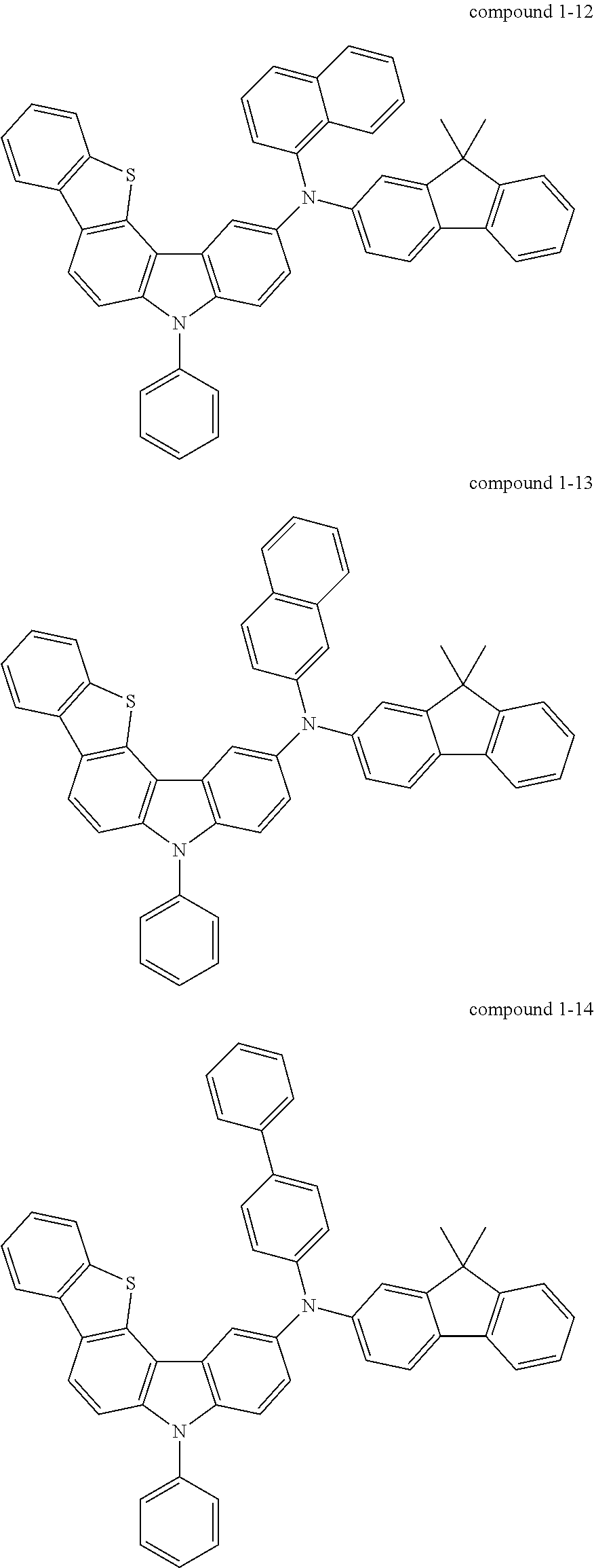


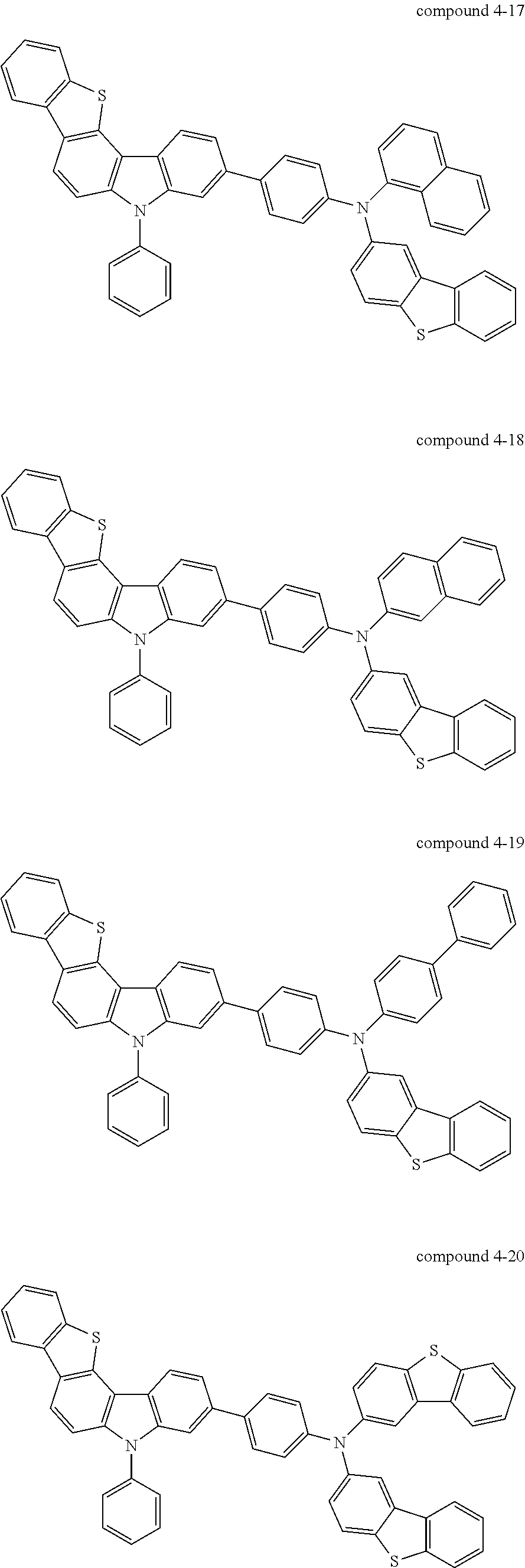


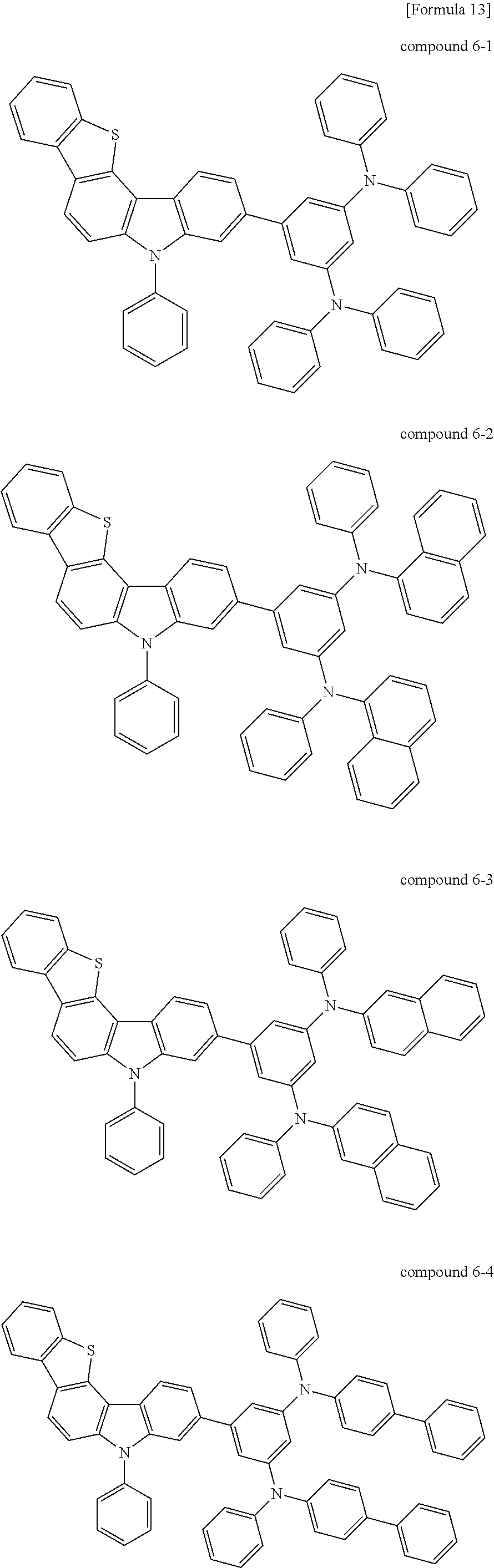


| TABLE 1 | ||||||
| hole | ||||||
| transport | current | luminous | chromaticity | |||
| layer | voltage | density | efficiency | coordinate | ||
| material | (V) | (mA/cm2) | (cd/A) | (x, y) | ||
| Example 1 | compound | 5.4 | 13.92 | 8.7 | (0.15, 0.14) |
| 1-15 | |||||
| Example 2 | compound | 6.1 | 13.74 | 8.5 | (0.15, 0.15) |
| 2-10 | |||||
| Example 3 | compound | 5.1 | 14.11 | 9.0 | (0.15, 0.15) |
| 3-14 | |||||
| Example 4 | compound | 6.2 | 14.06 | 8.7 | (0.15, 0.14) |
| 4-8 | |||||
| Example 5 | compound | 5.5 | 13.92 | 8.8 | (0.15, 0.14) |
| 5-1 | |||||
| Example 6 | compound | 6.0 | 13.88 | 8.4 | (0.15, 0.15) |
| 6-3 | |||||
| Comparative | ADN | 7.1 | 13.47 | 7.5 | (0.15, 0.15) |
| Example 1 | |||||
Claims (11)


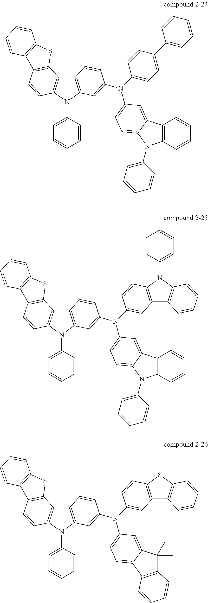


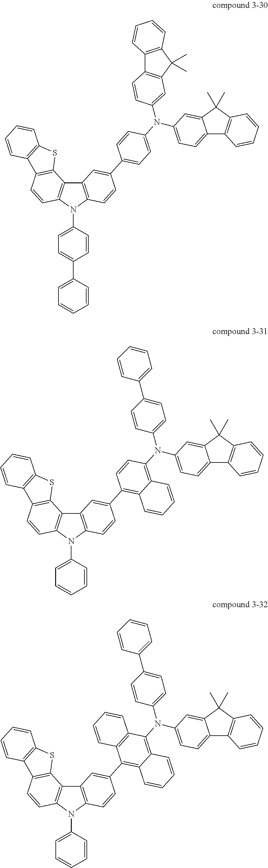


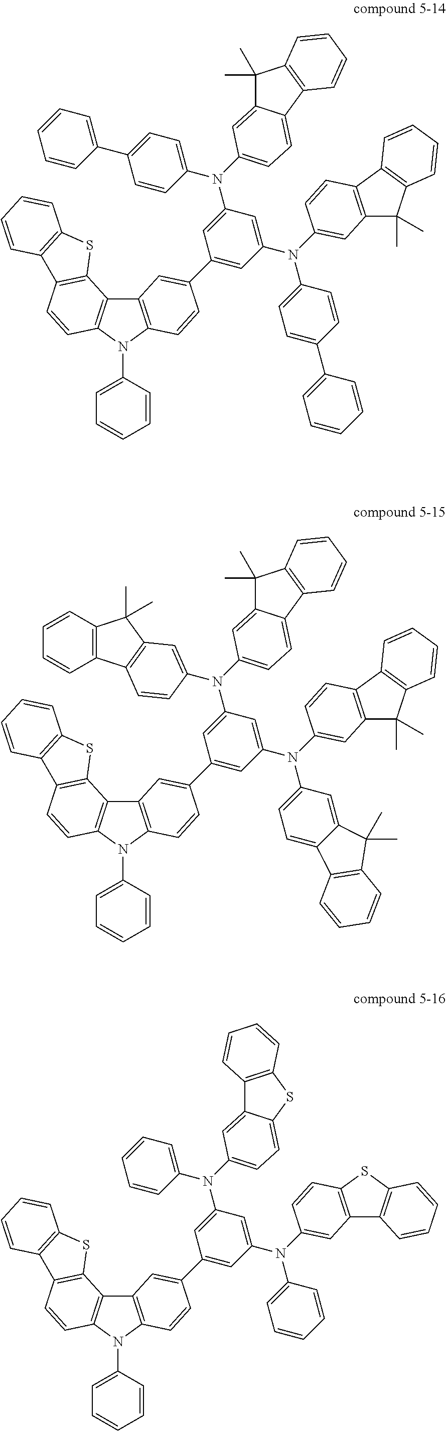


Applications Claiming Priority (3)
| Application Number | Priority Date | Filing Date | Title |
|---|---|---|---|
| KR10-2010-0049325 | 2010-05-26 | ||
| KR1020100049325A KR20110129766A (en) | 2010-05-26 | 2010-05-26 | Compound containing five membered heterocyclic compound, and organic electronic element using the same, terminal thereof |
| PCT/KR2011/003862 WO2011149283A2 (en) | 2010-05-26 | 2011-05-26 | Compound comprising a five-membered hetero ring, an organic electrical element using the same and a terminal thereof |
Related Parent Applications (1)
| Application Number | Title | Priority Date | Filing Date |
|---|---|---|---|
| PCT/KR2011/003862 A-371-Of-International WO2011149283A2 (en) | 2010-05-26 | 2011-05-26 | Compound comprising a five-membered hetero ring, an organic electrical element using the same and a terminal thereof |
Related Child Applications (1)
| Application Number | Title | Priority Date | Filing Date |
|---|---|---|---|
| US14/685,376 Continuation-In-Part US9178163B2 (en) | 2010-05-26 | 2015-04-13 | Compound comprising a five-membered hetero ring, an organic electrical element using same and a terminal thereof |
Publications (2)
| Publication Number | Publication Date |
|---|---|
| US20130069049A1 US20130069049A1 (en) | 2013-03-21 |
| US9005779B2 true US9005779B2 (en) | 2015-04-14 |
Family
ID=45004578
Family Applications (1)
| Application Number | Title | Priority Date | Filing Date |
|---|---|---|---|
| US13/699,040 Active 2031-09-06 US9005779B2 (en) | 2010-05-26 | 2011-05-26 | Compound comprising a five-membered hetero ring, an organic electrical element using the same and a terminal thereof |
Country Status (3)
| Country | Link |
|---|---|
| US (1) | US9005779B2 (en) |
| KR (1) | KR20110129766A (en) |
| WO (1) | WO2011149283A2 (en) |
Families Citing this family (22)
| Publication number | Priority date | Publication date | Assignee | Title |
|---|---|---|---|---|
| KR20120052879A (en) * | 2010-11-16 | 2012-05-24 | 롬엔드하스전자재료코리아유한회사 | Novel compound for organic electronic material and organic electroluminescent device using the same |
| KR101298483B1 (en) | 2011-04-01 | 2013-08-21 | 덕산하이메탈(주) | Chemical and Organic Electronic Element using the same, Electronic Device thereof |
| WO2013060418A1 (en) | 2011-10-27 | 2013-05-02 | Merck Patent Gmbh | Materials for electronic devices |
| KR20130053846A (en) * | 2011-11-16 | 2013-05-24 | 롬엔드하스전자재료코리아유한회사 | Novel organic electroluminescence compounds and organic electroluminescence device using the same |
| KR20130112342A (en) * | 2012-04-03 | 2013-10-14 | 롬엔드하스전자재료코리아유한회사 | Novel carbazole compounds and organic electroluminescence device containing the same |
| KR101488560B1 (en) * | 2012-05-08 | 2015-02-03 | 주식회사 두산 | Novel compounds and organic electro luminescence device using the same |
| KR101653338B1 (en) | 2013-08-05 | 2016-09-01 | 제일모직 주식회사 | Organic compound and organic optoelectric device and display device |
| KR102167048B1 (en) | 2013-12-03 | 2020-10-19 | 삼성디스플레이 주식회사 | Compound and organic light emitting device comprising same |
| US10797247B2 (en) * | 2014-07-24 | 2020-10-06 | Duk San Neolux Co., Ltd. | Compound for organic electric element, organic electric element comprising the same and electronic device thereof |
| TWI691492B (en) | 2014-12-12 | 2020-04-21 | 美商亞比馬利股份有限公司 | Process for the preparation of 4-phenyldibenzothiophene |
| KR101923171B1 (en) * | 2015-05-27 | 2018-11-28 | 덕산네오룩스 주식회사 | Compound for organic electric element, organic electric element comprising the same and electronic device thereof |
| KR102333974B1 (en) * | 2015-06-12 | 2021-12-02 | 덕산네오룩스 주식회사 | Compound for organic electric element, organic electric element comprising the same and electronic device thereof |
| KR102417039B1 (en) * | 2015-08-20 | 2022-07-05 | 덕산네오룩스 주식회사 | Compound for organic electronic element, organic electronic element comprising the same, and electronic device thereof |
| KR102334857B1 (en) * | 2015-09-08 | 2021-12-06 | 덕산네오룩스 주식회사 | Compound for organic electronic element, organic electronic element using the same, and an electronic device thereof |
| EP3176161A1 (en) * | 2015-12-02 | 2017-06-07 | Umicore AG & Co. KG | Buchwald-hartwig arylation method for the preparation of tertiary amines |
| KR102504581B1 (en) * | 2016-02-23 | 2023-03-02 | 덕산네오룩스 주식회사 | Compound for organic electronic element, organic electronic element comprising the same, and electronic device thereof |
| KR102116161B1 (en) * | 2016-02-29 | 2020-05-27 | 주식회사 엘지화학 | Nitrogen-containing compound and organic electronic device using the same |
| US10573819B2 (en) * | 2016-04-01 | 2020-02-25 | Duk San Neolux Co., Ltd. | Compound for organic electronic element, organic electronic element comprising the same, and electronic device thereof |
| KR102580210B1 (en) | 2016-09-20 | 2023-09-21 | 덕산네오룩스 주식회사 | Compound for organic electric element, organic electric element comprising the same and electronic device thereof |
| KR102580212B1 (en) | 2016-09-22 | 2023-09-21 | 덕산네오룩스 주식회사 | Compound for organic electric element, organic electric element comprising the same and electronic device thereof |
| CN110698458A (en) * | 2019-10-30 | 2020-01-17 | 烟台显华化工科技有限公司 | Organic luminescent material and application thereof |
| CN111004241A (en) * | 2019-12-27 | 2020-04-14 | 烟台显华化工科技有限公司 | Organic compound and application thereof |
Citations (9)
| Publication number | Priority date | Publication date | Assignee | Title |
|---|---|---|---|---|
| US20060147753A1 (en) | 2005-01-06 | 2006-07-06 | Byung-Hee Sohn | Blue-emitting polymer and organic electroluminescent device using the same |
| JP2007077033A (en) | 2005-09-12 | 2007-03-29 | Jsr Corp | Charge transporting compound and method for producing the same, composition for organic electroluminescent element and organic electroluminescent element |
| JP2008109103A (en) | 2006-09-27 | 2008-05-08 | Fujifilm Corp | Organic electroluminescent element |
| US20080198105A1 (en) * | 2005-06-17 | 2008-08-21 | Seung Rok Shin | Organic Light-Emitting Display Device and Driving Method Thereof |
| US20100012931A1 (en) * | 2008-06-05 | 2010-01-21 | Idemitsu Kosan Co., Ltd. | Polycyclic compounds and organic electroluminescence device employing the same |
| US20120018717A1 (en) | 2009-03-30 | 2012-01-26 | Duksan High Metal Co., Ltd. | Organic electronic device, compounds for same, and terminal |
| US20120080670A1 (en) | 2009-05-13 | 2012-04-05 | Samsung Mobile Display Co., Ltd. | Compound containing a 5-membered heterocycle and organic light-emitting diode using same, and terminal for same |
| US20120168734A1 (en) | 2009-08-11 | 2012-07-05 | Duksan High Metal Co., Ltd. | Compound containing 5-membered heterocycles, organic light-emitting device using same, and terminal comprising the latter |
| US20120217492A1 (en) | 2009-11-05 | 2012-08-30 | Duksan High Metal Co., Ltd. | Organic compound, organic electronic device using same, and terminal for same |
-
2010
- 2010-05-26 KR KR1020100049325A patent/KR20110129766A/en active Application Filing
-
2011
- 2011-05-26 US US13/699,040 patent/US9005779B2/en active Active
- 2011-05-26 WO PCT/KR2011/003862 patent/WO2011149283A2/en active Application Filing
Patent Citations (11)
| Publication number | Priority date | Publication date | Assignee | Title |
|---|---|---|---|---|
| US20060147753A1 (en) | 2005-01-06 | 2006-07-06 | Byung-Hee Sohn | Blue-emitting polymer and organic electroluminescent device using the same |
| KR20060080726A (en) | 2005-01-06 | 2006-07-11 | 삼성에스디아이 주식회사 | Blue electroluminescent polymer and organoelectroluminescent device employing the same |
| US7550207B2 (en) | 2005-01-06 | 2009-06-23 | Samsung Mobile Display Co., Ltd. | Blue-emitting polymer and organic electroluminescent device using the same |
| US20080198105A1 (en) * | 2005-06-17 | 2008-08-21 | Seung Rok Shin | Organic Light-Emitting Display Device and Driving Method Thereof |
| JP2007077033A (en) | 2005-09-12 | 2007-03-29 | Jsr Corp | Charge transporting compound and method for producing the same, composition for organic electroluminescent element and organic electroluminescent element |
| JP2008109103A (en) | 2006-09-27 | 2008-05-08 | Fujifilm Corp | Organic electroluminescent element |
| US20100012931A1 (en) * | 2008-06-05 | 2010-01-21 | Idemitsu Kosan Co., Ltd. | Polycyclic compounds and organic electroluminescence device employing the same |
| US20120018717A1 (en) | 2009-03-30 | 2012-01-26 | Duksan High Metal Co., Ltd. | Organic electronic device, compounds for same, and terminal |
| US20120080670A1 (en) | 2009-05-13 | 2012-04-05 | Samsung Mobile Display Co., Ltd. | Compound containing a 5-membered heterocycle and organic light-emitting diode using same, and terminal for same |
| US20120168734A1 (en) | 2009-08-11 | 2012-07-05 | Duksan High Metal Co., Ltd. | Compound containing 5-membered heterocycles, organic light-emitting device using same, and terminal comprising the latter |
| US20120217492A1 (en) | 2009-11-05 | 2012-08-30 | Duksan High Metal Co., Ltd. | Organic compound, organic electronic device using same, and terminal for same |
Non-Patent Citations (1)
| Title |
|---|
| International Search Report (in Korean with English translation) and Written Opinion (in Korean) for PCT/KR2011/003862, mailed Feb. 6, 2012. |
Also Published As
| Publication number | Publication date |
|---|---|
| KR20110129766A (en) | 2011-12-02 |
| WO2011149283A2 (en) | 2011-12-01 |
| US20130069049A1 (en) | 2013-03-21 |
| WO2011149283A9 (en) | 2012-07-12 |
| WO2011149283A3 (en) | 2012-04-19 |
Similar Documents
| Publication | Publication Date | Title |
|---|---|---|
| US9005779B2 (en) | Compound comprising a five-membered hetero ring, an organic electrical element using the same and a terminal thereof | |
| US9079920B2 (en) | Compound containing 5-membered heterocycles, organic light-emitting device using same, and terminal comprising the latter | |
| US8889271B2 (en) | Compound containing a 5-membered heterocycle and organic light-emitting diode using same, and terminal for same | |
| US9102616B2 (en) | Organic compound, organic electronic device using same, and terminal for same | |
| KR101604642B1 (en) | Compound Containing Five Membered heterocyclic compound, And Organic Electronic Element Using The Same, Terminal Thereof | |
| US9233923B2 (en) | Organic compounds for organic electronic devices and terminals | |
| US8507904B2 (en) | Compound including indole derivative, organic electronic element using same, and terminal thereof | |
| KR101188280B1 (en) | Compound Containing Carbazole and Aromatic Amine Derivative compound, And Organic Electronic Element Using The Same, Terminal Thereof | |
| KR101181266B1 (en) | Bisdiarylamine Chemical Comprising Carbazole Derivatives and Organic Electronic Element using the same, Terminal thereof | |
| KR101144358B1 (en) | Compound Containing 5-Membered Heterocycle And Organic Electronic Element Using The Same, Terminal Thereof | |
| KR101305934B1 (en) | Chemical and Organic Electronic Element using the same, Terminal thereof | |
| KR20110066763A (en) | Compound containing indoloacridine and organic electronic element using the same, terminal thereof | |
| KR101219475B1 (en) | Compound Containing Indoloacridine And Organic Electronic Element Using The Same, Terminal Thereof | |
| KR20110100877A (en) | Compound containing 5-membered heterocycle and organic electronic element using the same, terminal thereof | |
| US9290513B2 (en) | Compound containing 5-membered heterocycles, organic electronic device using same, and terminal comprising the latter | |
| US9017828B2 (en) | Compound including indole derivative in which two tertiary amines are substituted, organic electronic element using same, and terminal thereof | |
| US10991890B2 (en) | Compound containing a 5-membered heterocycle and organic light-emitting diode using same, and terminal for same | |
| KR101144357B1 (en) | Compound Containing dibenzocarbazole And Organic Electronic Element Using The Same, Terminal Thereof | |
| KR101181267B1 (en) | Chemical Comprising Naphthylcarbazole Derivatives and Organic Electronic Element using the same, Terminal thereof | |
| KR20100125928A (en) | Compound containing at least two 5-membered heterocycle and organic electronic element using the same, terminal thereof | |
| US9178163B2 (en) | Compound comprising a five-membered hetero ring, an organic electrical element using same and a terminal thereof | |
| KR101952234B1 (en) | Compound for organic electronic element, organic electronic element using the same, and a electronic device thereof | |
| KR101999545B1 (en) | Compound for organic electronic element, organic electronic element using the same, and a electronic device thereof | |
| KR101146930B1 (en) | Compound Containing At Least Two 5-Membered Heterocycle And Organic Electronic Element Using The Same, Terminal Thereof | |
| KR101172051B1 (en) | Chemical Comprising DiBenzopyrene Have Heterocyclic Ring and Organic Electronic Element using the same, Terminal thereof |
Legal Events
| Date | Code | Title | Description |
|---|---|---|---|
| AS | Assignment |
Owner name: DUKSAN HIGH METAL CO., LTD., KOREA, REPUBLIC OF Free format text: ASSIGNMENT OF ASSIGNORS INTEREST;ASSIGNORS:PARK, JUNGHWAN;KIM, DAESUNG;JI, HEESUN;AND OTHERS;REEL/FRAME:029327/0963 Effective date: 20121114 |
|
| AS | Assignment |
Owner name: DUK SAN NEOLUX CO., LTD., KOREA, REPUBLIC OF Free format text: ASSIGNMENT OF ASSIGNORS INTEREST;ASSIGNOR:DUKSAN HIGH METAL CO., LTD.;REEL/FRAME:034964/0908 Effective date: 20150115 |
|
| STCF | Information on status: patent grant |
Free format text: PATENTED CASE |
|
| MAFP | Maintenance fee payment |
Free format text: PAYMENT OF MAINTENANCE FEE, 4TH YR, SMALL ENTITY (ORIGINAL EVENT CODE: M2551); ENTITY STATUS OF PATENT OWNER: SMALL ENTITY Year of fee payment: 4 |
|
| MAFP | Maintenance fee payment |
Free format text: PAYMENT OF MAINTENANCE FEE, 8TH YR, SMALL ENTITY (ORIGINAL EVENT CODE: M2552); ENTITY STATUS OF PATENT OWNER: SMALL ENTITY Year of fee payment: 8 |