US8999614B2 - Photoresist composition for forming a color filter and display substrate - Google Patents
Photoresist composition for forming a color filter and display substrate Download PDFInfo
- Publication number
- US8999614B2 US8999614B2 US13/665,626 US201213665626A US8999614B2 US 8999614 B2 US8999614 B2 US 8999614B2 US 201213665626 A US201213665626 A US 201213665626A US 8999614 B2 US8999614 B2 US 8999614B2
- Authority
- US
- United States
- Prior art keywords
- red
- color filter
- compound
- colorant
- photoresist composition
- Prior art date
- Legal status (The legal status is an assumption and is not a legal conclusion. Google has not performed a legal analysis and makes no representation as to the accuracy of the status listed.)
- Active, expires
Links
- 229920002120 photoresistant polymer Polymers 0.000 title claims abstract description 76
- 239000000203 mixture Substances 0.000 title claims abstract description 75
- 239000000758 substrate Substances 0.000 title claims description 55
- 239000001062 red colorant Substances 0.000 claims abstract description 109
- 239000000126 substance Substances 0.000 claims abstract description 58
- 239000001060 yellow colorant Substances 0.000 claims abstract description 51
- 125000000008 (C1-C10) alkyl group Chemical group 0.000 claims abstract description 30
- 229910018828 PO3H2 Inorganic materials 0.000 claims abstract description 15
- 125000004435 hydrogen atom Chemical group [H]* 0.000 claims abstract description 15
- 238000004519 manufacturing process Methods 0.000 claims abstract description 13
- 150000001875 compounds Chemical class 0.000 claims description 53
- -1 xanthene compound Chemical class 0.000 claims description 42
- QDLAGTHXVHQKRE-UHFFFAOYSA-N lichenxanthone Natural products COC1=CC(O)=C2C(=O)C3=C(C)C=C(OC)C=C3OC2=C1 QDLAGTHXVHQKRE-UHFFFAOYSA-N 0.000 claims description 14
- CSHWQDPOILHKBI-UHFFFAOYSA-N peryrene Natural products C1=CC(C2=CC=CC=3C2=C2C=CC=3)=C3C2=CC=CC3=C1 CSHWQDPOILHKBI-UHFFFAOYSA-N 0.000 claims description 14
- 239000011230 binding agent Substances 0.000 claims description 12
- 239000000178 monomer Substances 0.000 claims description 9
- 239000003505 polymerization initiator Substances 0.000 claims description 9
- 239000002904 solvent Substances 0.000 claims description 9
- NIXOWILDQLNWCW-UHFFFAOYSA-M Acrylate Chemical compound [O-]C(=O)C=C NIXOWILDQLNWCW-UHFFFAOYSA-M 0.000 description 22
- 230000003247 decreasing effect Effects 0.000 description 19
- 150000004696 coordination complex Chemical class 0.000 description 16
- 238000002834 transmittance Methods 0.000 description 12
- 239000010409 thin film Substances 0.000 description 11
- 239000003086 colorant Substances 0.000 description 9
- 239000002585 base Substances 0.000 description 8
- 229920005989 resin Polymers 0.000 description 7
- 239000011347 resin Substances 0.000 description 7
- TXBCBTDQIULDIA-UHFFFAOYSA-N 2-[[3-hydroxy-2,2-bis(hydroxymethyl)propoxy]methyl]-2-(hydroxymethyl)propane-1,3-diol Chemical compound OCC(CO)(CO)COCC(CO)(CO)CO TXBCBTDQIULDIA-UHFFFAOYSA-N 0.000 description 6
- 239000004973 liquid crystal related substance Substances 0.000 description 6
- 150000002894 organic compounds Chemical class 0.000 description 6
- 238000010791 quenching Methods 0.000 description 6
- QGKMIGUHVLGJBR-UHFFFAOYSA-M (4z)-1-(3-methylbutyl)-4-[[1-(3-methylbutyl)quinolin-1-ium-4-yl]methylidene]quinoline;iodide Chemical compound [I-].C12=CC=CC=C2N(CCC(C)C)C=CC1=CC1=CC=[N+](CCC(C)C)C2=CC=CC=C12 QGKMIGUHVLGJBR-UHFFFAOYSA-M 0.000 description 5
- WXZMFSXDPGVJKK-UHFFFAOYSA-N pentaerythritol Chemical compound OCC(CO)(CO)CO WXZMFSXDPGVJKK-UHFFFAOYSA-N 0.000 description 5
- 239000000049 pigment Substances 0.000 description 5
- 230000000171 quenching effect Effects 0.000 description 5
- ARXJGSRGQADJSQ-UHFFFAOYSA-N 1-methoxypropan-2-ol Chemical compound COCC(C)O ARXJGSRGQADJSQ-UHFFFAOYSA-N 0.000 description 4
- GJCOSYZMQJWQCA-UHFFFAOYSA-N 9H-xanthene Chemical compound C1=CC=C2CC3=CC=CC=C3OC2=C1 GJCOSYZMQJWQCA-UHFFFAOYSA-N 0.000 description 4
- 125000002080 perylenyl group Chemical group C1(=CC=C2C=CC=C3C4=CC=CC5=CC=CC(C1=C23)=C45)* 0.000 description 4
- 230000003252 repetitive effect Effects 0.000 description 4
- LYCAIKOWRPUZTN-UHFFFAOYSA-N Ethylene glycol Chemical compound OCCO LYCAIKOWRPUZTN-UHFFFAOYSA-N 0.000 description 3
- DNIAPMSPPWPWGF-UHFFFAOYSA-N Propylene glycol Chemical compound CC(O)CO DNIAPMSPPWPWGF-UHFFFAOYSA-N 0.000 description 3
- MTHSVFCYNBDYFN-UHFFFAOYSA-N diethylene glycol Chemical compound OCCOCCO MTHSVFCYNBDYFN-UHFFFAOYSA-N 0.000 description 3
- 238000002513 implantation Methods 0.000 description 3
- 229910052751 metal Inorganic materials 0.000 description 3
- 239000002184 metal Substances 0.000 description 3
- 238000012986 modification Methods 0.000 description 3
- 230000004048 modification Effects 0.000 description 3
- KWOLFJPFCHCOCG-UHFFFAOYSA-N Acetophenone Chemical compound CC(=O)C1=CC=CC=C1 KWOLFJPFCHCOCG-UHFFFAOYSA-N 0.000 description 2
- JMASRVWKEDWRBT-UHFFFAOYSA-N Gallium nitride Chemical compound [Ga]#N JMASRVWKEDWRBT-UHFFFAOYSA-N 0.000 description 2
- PEDCQBHIVMGVHV-UHFFFAOYSA-N Glycerine Chemical compound OCC(O)CO PEDCQBHIVMGVHV-UHFFFAOYSA-N 0.000 description 2
- ISAOCJYIOMOJEB-UHFFFAOYSA-N benzoin Chemical compound C=1C=CC=CC=1C(O)C(=O)C1=CC=CC=C1 ISAOCJYIOMOJEB-UHFFFAOYSA-N 0.000 description 2
- IISBACLAFKSPIT-UHFFFAOYSA-N bisphenol A Chemical compound C=1C=C(O)C=CC=1C(C)(C)C1=CC=C(O)C=C1 IISBACLAFKSPIT-UHFFFAOYSA-N 0.000 description 2
- 229920003986 novolac Polymers 0.000 description 2
- 230000003287 optical effect Effects 0.000 description 2
- LLHKCFNBLRBOGN-UHFFFAOYSA-N propylene glycol methyl ether acetate Chemical compound COCC(C)OC(C)=O LLHKCFNBLRBOGN-UHFFFAOYSA-N 0.000 description 2
- VNQXSTWCDUXYEZ-UHFFFAOYSA-N 1,7,7-trimethylbicyclo[2.2.1]heptane-2,3-dione Chemical compound C1CC2(C)C(=O)C(=O)C1C2(C)C VNQXSTWCDUXYEZ-UHFFFAOYSA-N 0.000 description 1
- OYNPGVKMHISHLS-UHFFFAOYSA-N 1-benzylphenanthrene-9,10-dione Chemical compound C1=CC=C2C3=CC=CC=C3C(=O)C(=O)C2=C1CC1=CC=CC=C1 OYNPGVKMHISHLS-UHFFFAOYSA-N 0.000 description 1
- VFDYEMVVNIPATA-UHFFFAOYSA-N 2-ethyl-2-(hydroxymethyl)propane-1,3-diol;propane-1,2,3-triol Chemical compound OCC(O)CO.CCC(CO)(CO)CO VFDYEMVVNIPATA-UHFFFAOYSA-N 0.000 description 1
- SJEBAWHUJDUKQK-UHFFFAOYSA-N 2-ethylanthraquinone Chemical compound C1=CC=C2C(=O)C3=CC(CC)=CC=C3C(=O)C2=C1 SJEBAWHUJDUKQK-UHFFFAOYSA-N 0.000 description 1
- 239000004925 Acrylic resin Substances 0.000 description 1
- 229920000178 Acrylic resin Polymers 0.000 description 1
- VYZAMTAEIAYCRO-UHFFFAOYSA-N Chromium Chemical compound [Cr] VYZAMTAEIAYCRO-UHFFFAOYSA-N 0.000 description 1
- 239000004593 Epoxy Substances 0.000 description 1
- IAYPIBMASNFSPL-UHFFFAOYSA-N Ethylene oxide Chemical compound C1CO1 IAYPIBMASNFSPL-UHFFFAOYSA-N 0.000 description 1
- 229910002601 GaN Inorganic materials 0.000 description 1
- BPQQTUXANYXVAA-UHFFFAOYSA-N Orthosilicate Chemical compound [O-][Si]([O-])([O-])[O-] BPQQTUXANYXVAA-UHFFFAOYSA-N 0.000 description 1
- GOOHAUXETOMSMM-UHFFFAOYSA-N Propylene oxide Chemical compound CC1CO1 GOOHAUXETOMSMM-UHFFFAOYSA-N 0.000 description 1
- 244000028419 Styrax benzoin Species 0.000 description 1
- 235000000126 Styrax benzoin Nutrition 0.000 description 1
- 235000008411 Sumatra benzointree Nutrition 0.000 description 1
- ZJCCRDAZUWHFQH-UHFFFAOYSA-N Trimethylolpropane Chemical compound CCC(CO)(CO)CO ZJCCRDAZUWHFQH-UHFFFAOYSA-N 0.000 description 1
- SNBIRMPHXIQCBU-UHFFFAOYSA-N [Al+3].[O-2].[Y+3].[Ce+3] Chemical compound [Al+3].[O-2].[Y+3].[Ce+3] SNBIRMPHXIQCBU-UHFFFAOYSA-N 0.000 description 1
- 239000002253 acid Substances 0.000 description 1
- 150000001252 acrylic acid derivatives Chemical class 0.000 description 1
- 239000003513 alkali Substances 0.000 description 1
- 125000000217 alkyl group Chemical group 0.000 description 1
- 229960002130 benzoin Drugs 0.000 description 1
- RWCCWEUUXYIKHB-UHFFFAOYSA-N benzophenone Chemical compound C=1C=CC=CC=1C(=O)C1=CC=CC=C1 RWCCWEUUXYIKHB-UHFFFAOYSA-N 0.000 description 1
- 239000012965 benzophenone Substances 0.000 description 1
- 229930006711 bornane-2,3-dione Natural products 0.000 description 1
- WERYXYBDKMZEQL-UHFFFAOYSA-N butane-1,4-diol Chemical compound OCCCCO WERYXYBDKMZEQL-UHFFFAOYSA-N 0.000 description 1
- 229910052804 chromium Inorganic materials 0.000 description 1
- 239000011651 chromium Substances 0.000 description 1
- 230000001419 dependent effect Effects 0.000 description 1
- VFHVQBAGLAREND-UHFFFAOYSA-N diphenylphosphoryl-(2,4,6-trimethylphenyl)methanone Chemical compound CC1=CC(C)=CC(C)=C1C(=O)P(=O)(C=1C=CC=CC=1)C1=CC=CC=C1 VFHVQBAGLAREND-UHFFFAOYSA-N 0.000 description 1
- 229940117927 ethylene oxide Drugs 0.000 description 1
- 230000005281 excited state Effects 0.000 description 1
- 235000011187 glycerol Nutrition 0.000 description 1
- 235000019382 gum benzoic Nutrition 0.000 description 1
- XXMIOPMDWAUFGU-UHFFFAOYSA-N hexane-1,6-diol Chemical compound OCCCCCCO XXMIOPMDWAUFGU-UHFFFAOYSA-N 0.000 description 1
- 125000004051 hexyl group Chemical group [H]C([H])([H])C([H])([H])C([H])([H])C([H])([H])C([H])([H])C([H])([H])* 0.000 description 1
- 125000001183 hydrocarbyl group Chemical group 0.000 description 1
- 229910052738 indium Inorganic materials 0.000 description 1
- APFVFJFRJDLVQX-UHFFFAOYSA-N indium atom Chemical compound [In] APFVFJFRJDLVQX-UHFFFAOYSA-N 0.000 description 1
- 238000012538 light obscuration Methods 0.000 description 1
- 238000000034 method Methods 0.000 description 1
- 125000002496 methyl group Chemical group [H]C([H])([H])* 0.000 description 1
- YLHXLHGIAMFFBU-UHFFFAOYSA-N methyl phenylglyoxalate Chemical compound COC(=O)C(=O)C1=CC=CC=C1 YLHXLHGIAMFFBU-UHFFFAOYSA-N 0.000 description 1
- SLCVBVWXLSEKPL-UHFFFAOYSA-N neopentyl glycol Chemical compound OCC(C)(C)CO SLCVBVWXLSEKPL-UHFFFAOYSA-N 0.000 description 1
- 150000004767 nitrides Chemical class 0.000 description 1
- 150000002923 oximes Chemical class 0.000 description 1
- 150000003254 radicals Chemical class 0.000 description 1
- 150000003839 salts Chemical class 0.000 description 1
- 229920006395 saturated elastomer Polymers 0.000 description 1
- 125000001424 substituent group Chemical group 0.000 description 1
- YRHRIQCWCFGUEQ-UHFFFAOYSA-N thioxanthen-9-one Chemical compound C1=CC=C2C(=O)C3=CC=CC=C3SC2=C1 YRHRIQCWCFGUEQ-UHFFFAOYSA-N 0.000 description 1
- 230000007704 transition Effects 0.000 description 1
- ZIBGPFATKBEMQZ-UHFFFAOYSA-N triethylene glycol Chemical compound OCCOCCOCCO ZIBGPFATKBEMQZ-UHFFFAOYSA-N 0.000 description 1
- 229910019901 yttrium aluminum garnet Inorganic materials 0.000 description 1
Images


Classifications
-
- G—PHYSICS
- G02—OPTICS
- G02B—OPTICAL ELEMENTS, SYSTEMS OR APPARATUS
- G02B5/00—Optical elements other than lenses
- G02B5/20—Filters
- G02B5/22—Absorbing filters
- G02B5/223—Absorbing filters containing organic substances, e.g. dyes, inks or pigments
-
- G—PHYSICS
- G02—OPTICS
- G02B—OPTICAL ELEMENTS, SYSTEMS OR APPARATUS
- G02B5/00—Optical elements other than lenses
- G02B5/20—Filters
-
- G—PHYSICS
- G02—OPTICS
- G02B—OPTICAL ELEMENTS, SYSTEMS OR APPARATUS
- G02B5/00—Optical elements other than lenses
- G02B5/20—Filters
- G02B5/201—Filters in the form of arrays
-
- G—PHYSICS
- G03—PHOTOGRAPHY; CINEMATOGRAPHY; ANALOGOUS TECHNIQUES USING WAVES OTHER THAN OPTICAL WAVES; ELECTROGRAPHY; HOLOGRAPHY
- G03F—PHOTOMECHANICAL PRODUCTION OF TEXTURED OR PATTERNED SURFACES, e.g. FOR PRINTING, FOR PROCESSING OF SEMICONDUCTOR DEVICES; MATERIALS THEREFOR; ORIGINALS THEREFOR; APPARATUS SPECIALLY ADAPTED THEREFOR
- G03F7/00—Photomechanical, e.g. photolithographic, production of textured or patterned surfaces, e.g. printing surfaces; Materials therefor, e.g. comprising photoresists; Apparatus specially adapted therefor
- G03F7/0005—Production of optical devices or components in so far as characterised by the lithographic processes or materials used therefor
- G03F7/0007—Filters, e.g. additive colour filters; Components for display devices
-
- G—PHYSICS
- G03—PHOTOGRAPHY; CINEMATOGRAPHY; ANALOGOUS TECHNIQUES USING WAVES OTHER THAN OPTICAL WAVES; ELECTROGRAPHY; HOLOGRAPHY
- G03F—PHOTOMECHANICAL PRODUCTION OF TEXTURED OR PATTERNED SURFACES, e.g. FOR PRINTING, FOR PROCESSING OF SEMICONDUCTOR DEVICES; MATERIALS THEREFOR; ORIGINALS THEREFOR; APPARATUS SPECIALLY ADAPTED THEREFOR
- G03F7/00—Photomechanical, e.g. photolithographic, production of textured or patterned surfaces, e.g. printing surfaces; Materials therefor, e.g. comprising photoresists; Apparatus specially adapted therefor
- G03F7/004—Photosensitive materials
- G03F7/0042—Photosensitive materials with inorganic or organometallic light-sensitive compounds not otherwise provided for, e.g. inorganic resists
-
- G—PHYSICS
- G03—PHOTOGRAPHY; CINEMATOGRAPHY; ANALOGOUS TECHNIQUES USING WAVES OTHER THAN OPTICAL WAVES; ELECTROGRAPHY; HOLOGRAPHY
- G03F—PHOTOMECHANICAL PRODUCTION OF TEXTURED OR PATTERNED SURFACES, e.g. FOR PRINTING, FOR PROCESSING OF SEMICONDUCTOR DEVICES; MATERIALS THEREFOR; ORIGINALS THEREFOR; APPARATUS SPECIALLY ADAPTED THEREFOR
- G03F7/00—Photomechanical, e.g. photolithographic, production of textured or patterned surfaces, e.g. printing surfaces; Materials therefor, e.g. comprising photoresists; Apparatus specially adapted therefor
- G03F7/004—Photosensitive materials
- G03F7/0045—Photosensitive materials with organic non-macromolecular light-sensitive compounds not otherwise provided for, e.g. dissolution inhibitors
-
- G—PHYSICS
- G03—PHOTOGRAPHY; CINEMATOGRAPHY; ANALOGOUS TECHNIQUES USING WAVES OTHER THAN OPTICAL WAVES; ELECTROGRAPHY; HOLOGRAPHY
- G03F—PHOTOMECHANICAL PRODUCTION OF TEXTURED OR PATTERNED SURFACES, e.g. FOR PRINTING, FOR PROCESSING OF SEMICONDUCTOR DEVICES; MATERIALS THEREFOR; ORIGINALS THEREFOR; APPARATUS SPECIALLY ADAPTED THEREFOR
- G03F7/00—Photomechanical, e.g. photolithographic, production of textured or patterned surfaces, e.g. printing surfaces; Materials therefor, e.g. comprising photoresists; Apparatus specially adapted therefor
- G03F7/004—Photosensitive materials
- G03F7/027—Non-macromolecular photopolymerisable compounds having carbon-to-carbon double bonds, e.g. ethylenic compounds
-
- G—PHYSICS
- G03—PHOTOGRAPHY; CINEMATOGRAPHY; ANALOGOUS TECHNIQUES USING WAVES OTHER THAN OPTICAL WAVES; ELECTROGRAPHY; HOLOGRAPHY
- G03F—PHOTOMECHANICAL PRODUCTION OF TEXTURED OR PATTERNED SURFACES, e.g. FOR PRINTING, FOR PROCESSING OF SEMICONDUCTOR DEVICES; MATERIALS THEREFOR; ORIGINALS THEREFOR; APPARATUS SPECIALLY ADAPTED THEREFOR
- G03F7/00—Photomechanical, e.g. photolithographic, production of textured or patterned surfaces, e.g. printing surfaces; Materials therefor, e.g. comprising photoresists; Apparatus specially adapted therefor
- G03F7/004—Photosensitive materials
- G03F7/09—Photosensitive materials characterised by structural details, e.g. supports, auxiliary layers
- G03F7/105—Photosensitive materials characterised by structural details, e.g. supports, auxiliary layers having substances, e.g. indicators, for forming visible images
Definitions
- This disclosure relates to a photoresist composition for manufacturing a color filter and a display substrate. Additionally this disclosure relates to a photoresist composition for manufacturing a color filter used for a display apparatus and a display substrate.
- a display apparatus includes a display panel displaying an image using light and a light providing assembly providing the light to the display panel.
- the display panel includes a planarity of pixel cells, a switching element, a pixel electrode, a common electrode and a color filter.
- the display panel may use a liquid crystal as a display element.
- a white light provided to the display panel from the light providing assembly passes through a liquid crystal layer including the liquid crystal and the color filter so that the display panel displays a color image generated from a variable color mixture of light.
- the display panel includes a red color filter (“R”), a green color filter (“G”) and a blue color filter (“B”), and three color lights, which are converted by the color filters of the display panel are mixed to represent various colors.
- a pigment as a colorant representing a color has been used in each of the color filters.
- a dye is used with the pigment in order to improve the brightness.
- a hybrid type colorant including the pigment and the dye is used, the brightness is marginally improved.
- a dye having a high luminance may be used to maximize the brightness while excluding the pigment.
- the colorant includes only the dye, an entire brightness may be improved. However, a black brightness is increased so that the contrast ratio is undesirably decreased. Thus, there remains a need for an improved colorant.
- a photoresist composition for manufacturing a color filter capable of controlling a fluorescence of a colorant to improve a contrast ratio is provided.
- a display substrate including a color filter manufactured by the photoresist composition is provided.
- a photoresist composition for manufacturing a color filter includes a first red colorant; and a yellow colorant represented by Chemical Formula 1,
- R 1 and R 2 each independently represent a C1 to C10 alkyl group
- a 1 , A 2 , A 3 , and A 4 each independently represent a C1 to C10 alkyl group, —CN, —PO 3 H 2 , —C(O)OH, or a hydrogen atom
- m is an integer of 1 to 10
- at least one —CH 2 — of R 1 and R 2 if present is independently replaced with —O—, —C(O)—, —C(O)O—, or —OC(O)—.
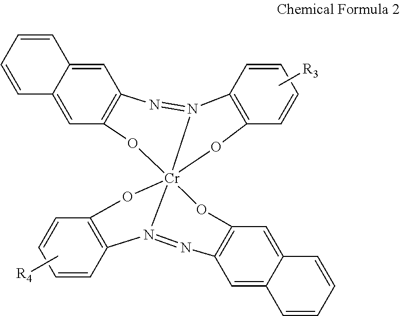
- the first red colorant of the photoresist composition may be represented by Chemical Formula 2,
- R 3 and R 4 each independently represent a C1 to C10 alkyl group
- a 1 , A 2 , A 3 , and A 4 each independently represent a C1 to C10 alkyl group, —CN, —PO 3 H 2 , —C(O)OH, or a hydrogen atom
- m is an integer of 1 to 10
- at least one —CH 2 — of R 3 and R 4 if present is independently replaced with —O—, —C(O)—, —C(O)O— or —OC(O)—.
- the photoresist composition may further include a second red colorant having a different structure from the first red colorant.
- the second red colorant may include at least one of a xanthene compound, a cyanine compound, an azo compound, a perylene compound, or a compound represented by Chemical Formula 3.
- n may represent an integer of 3 or 4.
- the first red colorant of the photoresist composition may include at least one of a xanthene compound, a cyanine compound, an azo compound, a perylene compound or a compound represent by the above Chemical Formula 3.
- a second red colorant may be included in the photoresist composition, and the second red colorant may be a different compound from the first red colorant, and may include at least one of a xanthene compound, a cyanine compound, an azo compound, a perylene compound or a compound represented by the above Chemical Formula 3.
- the photoresist composition may further include a photo-polymerization initiator, a monomer, a binder, and a solvent.
- a photoresist composition includes a yellow colorant and a first red colorant represented by Chemical Formula 2,
- R 3 and R 4 each independently represent a C1 to C10 alkyl group
- a 1 , A 2 , A 3 , and A 4 each independently represent a C1 to C10 alkyl group, —CN, —PO 3 H 2 , —C(O)OH, or a hydrogen atom, m is an integer of 1 to 10, and
- the photoresist composition may further include a second red colorant represented by Chemical Formula 3,
- n may represent an integer of 3 or 4.
- a display substrate includes a red color filter including a first red colorant and a yellow colorant represented by Chemical Formula 1,
- R 1 and R 2 each independently represent a C1 to C10 alkyl group
- a 1 , A 2 , A 3 , and A 4 each independently represent a C1 to C10 alkyl group, —CN, —PO 3 H 2 , —C(O)OH, or a hydrogen atom
- m is an integer of 1 to 10
- at least one —CH 2 — of R 1 and R 2 if present is independently replaced with —O—, —C(O)—, —C(O)O—, or —OC(O)—.
- the first red colorant of the display substrate may be represented by the above Chemical Formula 2.
- the first red colorant of the display substrate may include at least one of a xanthene compound, a cyanine compound, an azo compound, a perylene compound or a compound represented by Chemical Formula 3.
- n may represent an integer of 3 or 4.
- the red color filter of the display substrate may further include a second red colorant including at least one of a xanthene compound, a cyanine compound, an azo compound, a perylene compound or a compound represented by the above Chemical Formula 3.
- the second red colorant may be different than the first red colorant.
- the display substrate may further include a switching element disposed on a base substrate and a pixel electrode connected to the switching element, and the red color filter may be disposed between the switching element and the pixel electrode.
- the display substrate may further include a common electrode disposed on the red color filter.
- the red color filter of the display substrate may have a thickness in a range of about 1.0 micrometer ( ⁇ m) to about 3.5 ⁇ m.
- the display substrate includes a red color filter including a first red colorant represented by the above Chemical Formula 2 and a yellow colorant.
- the red color filter may further include a second red colorant represented by the above Chemical Formula 3.
- a fluorescent metal complex including a metal may be used as a red colorant for forming a red color filter.
- a brightness of a white display mode may be increased and a light emitting intensity of a black display mode may be decreased to improve a contrast ratio.
- a metal complex may be used as a yellow colorant for forming a red color filter so that the red colorant may not irradiate the fluorescence since the energy may become extinct by the yellow colorant when an energy transition is generated in the red colorant. Therefore, while not wishing to be bound by theory, it is believed the brightness of the black display mode may be decreased to improve a contrast ratio.
- FIG. 1 is a graph illustrating a light-transmittance (percent, %) versus a wavelength (nanometers, m) in a yellow colorant of a photoresist composition for manufacturing a color filter in accordance with an embodiment
- FIG. 2 is a graph illustrating a light-transmittance (percent, %) versus a wavelength (nanometers, m) of color filters formed using photoresist compositions;
- FIG. 3 is a graph illustrating a light-emitting intensity (arbitrary units) versus a wavelength (nanometers, m) of a photoresist composition
- FIG. 4 is a cross-sectional view illustrating a display apparatus including a display substrate in accordance with another embodiment.
- FIG. 5 is a cross-sectional view illustrating a display apparatus including a display substrate in accordance with still another embodiment.
- Embodiments are described herein with reference to cross sectional illustrations that are schematic illustrations of idealized embodiments (and intermediate structures). As such, variations from the shapes of the illustrations as a result, for example, of manufacturing techniques and/or tolerances, are to be expected. Thus, embodiments described herein should not be construed as limited to the particular shapes of regions as illustrated herein but are to include deviations in shapes that result, for example, from manufacturing. For example, a region illustrated or described as flat may, typically, have rough and/or nonlinear features. A region illustrated as a rectangle may typically have rounded or curved features. Moreover, sharp angles that are illustrated may be rounded.
- a buried region formed by implantation may result in some implantation in the region between the buried region and the surface through which the implantation takes place.
- the regions illustrated in the figures are schematic in nature and their shapes are not intended to illustrate the precise shape of a region and are not intended to limit the scope of the present disclosure.
- spatially relative terms such as “beneath”, “below”, “lower”, “above”, “upper”, and the like, may be used herein for ease of description to describe one element or feature's relationship to another element(s) or feature(s) as illustrated in the figures. It will be understood that the spatially relative terms are intended to encompass different orientations of the apparatus in use or operation in addition to the orientation depicted in the figures. For example, if the apparatus in the figures is turned over, elements described as “beneath”, “below”, or “lower” other elements or features would then be oriented “above”, or “upper” the other elements or features. Thus, the exemplary term “below” can encompass both an orientation above and below.
- the apparatus may be otherwise oriented (rotated 90 degrees or at other orientations) and the spatially relative descriptors used herein interpreted accordingly.
- Alkyl means a straight or branched chain, saturated, monovalent hydrocarbon group (e.g., methyl or hexyl).
- the term “*” represents a point of attachment of the indicated substituent.
- a photoresist composition for manufacturing a color filter includes a first red colorant, a yellow colorant and a second red colorant.
- the first and second red colorants and the yellow colorant may each be a dye.
- a red reproducibility of a color filter formed using the photoresist composition may be selected by selecting a content of the first red colorant, the second red colorant and the yellow colorant.
- the photoresist composition may further include a binder such as a binder resin, a monomer, a photo-polymerization initiator, and a solvent with the first red colorant, the second red colorant, and the yellow colorant.
- a binder such as a binder resin, a monomer, a photo-polymerization initiator, and a solvent with the first red colorant, the second red colorant, and the yellow colorant.
- the first and second red colorants each include an organic compound, which may fluoresce.
- each of the first and second red colorants may include at least one of a xanthene-based compound, a cyanine-based compound, an azo-based compound, a perylene-based compound or a compound represented by Chemical Formula 3 as the organic compound.
- the first red colorant may include the compound represented by Chemical Formula 3
- the second red colorant may include the azo-based compound.
- n may represent an integer of 3 or 4.
- each of the first and second red colorants may fluoresce, a brightness of a display apparatus including a color filter formed using the photoresist composition may be improved, as compared to a photoresist composition including a pigment.
- the yellow colorant may be represented by Chemical Formula 1.
- R 1 and R 2 each independently represent a C1 to C10 alkyl group
- a 1 , A 2 , A 3 , and A 4 each independently represent a C1 to C10 alkyl group, —CN, —PO 3 H 2 , —C(O)OH, or a hydrogen atom
- m is an integer of 1 to 10
- at least one —CH 2 — of R 1 and R 2 if present is independently replaced with —O—, —C(O)—, —C(O)O— or —OC(O)—.
- R 1 and/or R 2 may be represented by Chemical Formulae 1-1, 1-2, 1-3, 1-4, 1-5, 1-6, 1-7 or 1-8.
- At least one —CH 2 — of R 1 and R 2 can be replaced with —O—, —C(O)—, —C(O)O— or —OC(O)—.
- the yellow colorant has a metal complex structure including a metal.
- the yellow colorant may include chromium (e.g., Cr 6+ ).
- Cr 6+ chromium
- the first and the second red colorants either emit light or quench, dissipating the energy absorbed by the first and second red colorants.
- the yellow colorant has a metal complex structure to support the quenching of the first and second red colorants. While not wishing to be bound by theory, the light-emitting intensity of the first and second red colorants may be decreased by the yellow colorant, and thus the black brightness of the display apparatus may be decreased.
- an amount of the first red colorant may be about 25% by weight to about 65% by weight, specifically about 30% by weight to about 60% weight, more specifically about 40% by weight to about 50% by weight
- an amount of the second red colorant may be about 25% by weight to about 65% by weight, specifically about 30% by weight to about 60% weight, more specifically about 40% by weight to about 50% by weight
- an amount of the yellow colorant may be about 2% by weight to about 30% by weight, specifically about 4% by weight to about 25% weight, more specifically about 5% by weight and about 20% by weight.
- the total amount of the colorants included in the photoresist composition may be about 10% by weight to about 60% by weight, specifically about 20% by weight to about 50% by weight, more specifically about 30% by weight to about 40% by weight, based on a total weight of the photoresist composition. According to an embodiment, the total amount of the colorants included in the photoresist composition may be about 30% by weight to about 40% by weight, based on a total weight of the photoresist composition.
- FIG. 1 is a graph illustrating a light-transmittance (percent, %) versus a wavelength (nanometers, m) in a yellow colorant of a photoresist composition for manufacturing a color filter in accordance with an embodiment.
- a light-transmittance of the yellow colorant is equal to or greater than about 90% in a wavelength equal to or greater than about 580 nanometers (nm). While not wishing to be bound by theory, the yellow colorant may be used with the first and second red colorants to improve a brightness of a display apparatus including a color filter including the yellow colorant.
- a first display apparatus including a red color filter formed using a first photoresist composition which includes an azo-based compound as the first red colorant and the compound represented by the above Chemical Formula 3 as the second red colorant is compared with a second display apparatus substantially the same as the first display apparatus except for including a red color filter formed using a second photoresist composition which further includes a yellow colorant in addition to the azo-based compound and the compound represented by the above-Chemical Formula 3 of the first photoresist composition
- a brightness of the first display apparatus is defined to be “100%”
- a brightness of the second display apparatus is increased to be about 106%, with respect to the brightness of the first display apparatus.
- a contrast ratio of the second display apparatus is higher than that of the first display apparatus by about six times. While not wishing to be bound by theory, it is believed the yellow colorant having the metal complex structure improves the brightness and the black brightness is decreased, and thus the contrast ratio may be improved.
- the quenching may be increased.
- the yellow colorant is disposed adjacent to the first or second red colorants, the quenching may be facilitated.
- the black brightness may be decreased.
- the distance is dependent on a thickness of a color filter formed using the photoresist composition and thus, the quenching is increased when the thickness of the color filter is decreased.
- the binder resin, the monomer, the photo-polymerization initiator and the solvent included in the photoresist composition may be selected by one of skill in the art without undue experimentation.
- the photoresist composition may include a binder such as a binder resin, a monomer, a photo-polymerization initiator, and/or a solvent.
- the binder resin may include an acrylic resin, an alkali soluble resin e.g. a novolac resin, or the like.
- the binder resin is hardened in forming the color filter to define a shape of the color filter.
- Examples of the monomer may include ethylene glycol di(meth)acrylate, diethylene glycol di(meth)acrylate, triethylene glycol di(meth)acrylate, propylene glycol di(meth)acrylate, 1,4-butandiol di(meth)acrylate, 1,6-hexandiol di(meth)acrylate, neopentyl glycol di(meth)acrylate, pentaerythritol di(meth)acrylate, pentaerythritol tri(meth)acrylate, pentaerythritol tetra(meth)acrylate, pentaerythritol penta(meth)acrylate, pentaerythritol hexa(meth)acrylate, dipentaerythritol di(meth)acrylate, dipentaerythritol tri(meth)acrylate, dipentaerythritol tetra(meth)acrylate, dip
- Examples of the photo-polymerization initiator may include a triazine compound, an acetophenone-based compound, a biimidazole-based compound, an active radical generator such as a benzoin-based compound, a benzophenone-based compound, a thioxanthone-based compound, an oxime-based compound, 2,4,6-trimethylbenzoyldiphenylphosphine oxide, 10-butyl-2-chloroacrydone, 2-ethyl anthraquinone, benzyl-9,10-phenanthrenequinone, a camphor quinone, phenylglyoxylic acid methyl ester, a titanocene compound, an acid generator such as an onium salt, or the like. These may be used alone or a combination thereof.
- the solvent includes a compound capable of dispersing the first red colorant, the second red colorant, and the yellow colorant with the monomer and the photo-polymerization initiator.
- the solvent may include propylene glycol methyl ether acetate (“PGMEA”), propylene glycol methyl ether (“PGME”), or the like.
- the yellow colorant having the metal complex structure is used to provide improved brightness and the decreased black brightness, and thus the contrast ratio may be improved.
- the photoresist composition for manufacturing a color filter includes a first red colorant, a yellow colorant and a second red colorant.
- the first and second red colorants and the yellow colorant may each be a dye.
- a red reproducibility of a color filter formed using the photoresist composition may be controlled by a mixture of the first red colorant, the second red colorant and the yellow colorant.
- the photoresist composition includes a binder such as a binder resin, a monomer, a photo-polymerization initiator and a solvent.
- a binder such as a binder resin, a monomer, a photo-polymerization initiator and a solvent.
- the binder, monomer, photo-polymerization initiator and solvent are substantially the same as described above for the “photoresist composition-1.” Thus, any repetitive descriptions will be omitted.
- the first red colorant is a metal complex having fluorescence and represented by Chemical Formula 2.
- R 3 and R 4 each independently represent a C1 to C10 alkyl group
- a 1 , A 2 , A 3 , and A 4 each independently represent a C1 to C10 alkyl group, —CN, —PO 3 H 2 , —C(O)OH, or a hydrogen atom
- m is an integer of 1 to 10
- at least one —CH 2 — of R 3 and R 4 if present is independently replaced with —O—, —C(O)—, —C(O)O— or —OC(O)—.
- the first red colorant may be fluorescent.
- the first red colorant having a metal complex structure may have lower fluorescence than the second red colorant, which is an organic compound.
- the first red colorant can be fluorescent to improve a brightness of a display apparatus.
- a light-emitting intensity of the first red colorant is lower than the second red colorant, which is an organic compound, so that the first red colorant may prevent the black brightness from being increased.
- the second red colorant is an organic compound and may be fluorescent and examples of the second red colorant may include a xanthene-based compound, a cyanine-based compound, an azo-based compound, a perylene-based compound or a compound represented by Chemical Formula 3.
- n represents an integer of 1 to 4, specifically 3 or 4.
- the second red colorant may serve as a component of a red color filter improving a brightness of a display apparatus including the red color filter formed using the photoresist composition. While not wanting to be bound by theory, it is believed the first red colorant and the yellow colorant may support the second red colorant to improve a red color property of the red color filter and to control a black brightness.
- the yellow colorant may be substantially the same as the metal complex represented by Chemical Formula 1 and illustrated in the above “photoresist composition-1.” Thus, any repetitive descriptions will be omitted.
- the yellow colorant may decrease the light-emitting intensity of the first and second red colorants by the quenching described earlier.
- a brightness (Y) and a color coordinate (x, y) of each of the first and second red colorants and the yellow colorant may be as shown in Table 1.
- the red colorant which is an organic compound, changes the compound having the metal complex structure represented by Chemical Formula 2 so that an entire brightness of a display apparatus is increased and a black brightness is decreased to improve a contrast ratio.
- a first photoresist composition including an azo-based compound as a first red colorant and a cyanine-based compound as a second red colorant is prepared.
- a second photoresist composition according to another embodiment which further includes a yellow colorant, in addition to the azo-based compound as a first red colorant and the compound represented by the above Chemical Formula 3 as a second red colorant is prepared.
- a third photoresist composition according to yet another embodiment including a metal complex represented by Chemical Formula 2 as a first red colorant, the compound represented by Chemical Formula 3 as a second red colorant, and a yellow colorant represented by Chemical Formula 1 is prepared.
- a red color filter is formed using each of the first, second and third photoresist compositions, and a light-transmittance along a wavelength of the red color filters are measured and illustrated in FIG. 2 .
- FIG. 2 is a graph illustrating a light-transmittance (percent, %) versus a wavelength (nanometers, m) of color filters formed using photoresist compositions.
- a curve A represents the red color filter formed using the first photoresist composition
- a curve B represents the red color filter formed using the second photoresist composition
- a curve C represents the red color filter formed using the third photoresist composition.
- the black brightness may be effectively decreased by the red color filters formed using the second and third photoresist compositions, compared to the red color filter formed using the first photoresist composition.
- FIG. 3 is a graph illustrating a light-emitting intensity (arbitrary units) versus a wavelength (nanometers, m) of the photoresist compositions.
- a curve D represents the first photoresist composition
- a curve E represents the second photoresist composition
- a curve F represents the third photoresist composition.
- a maximum light-emitting intensity of the second photoresist composition is lower than that of the first photoresist composition.
- a maximum light-emitting intensity of the third photoresist composition is lower than that of the second photoresist composition.
- the third photoresist composition irradiates less in a range of about 490 nm to about 756 nm.
- a brightness of a display apparatus including a red color filter formed using the photoresist composition according to an embodiment may be improved and a black brightness may be minimized to improve a display quality.
- FIG. 4 is a cross-sectional view illustrating a display apparatus including a display substrate in accordance with another embodiment.
- a display apparatus 500 includes a light providing assembly 100 and a display panel 200 .
- the light providing assembly 100 includes a light-emitting module 110 , and the light-emitting module 110 is mounted on a printed circuit board 120 providing a driving signal to the light-emitting module 110 .
- the light-emitting module 110 provides a white light L 1 to the display panel 200 .
- the light providing assembly 100 may further include optical sheets and/or optical plates disposed between the light-emitting module 110 and the display panel 200 .
- the display panel 200 includes a first display substrate 210 , a second display substrate 220 and a liquid crystal layer 230 .
- the display panel 200 displays an image using the white light L 1 provided from the light providing assembly 100 .
- the second display substrate 220 faces the first display substrate 210 , and the liquid crystal layer 230 is interposed between the first and second display substrates 210 and 220 .
- a display substrate according to an embodiment may be the second display substrate 220 as illustrated schematically in FIG. 4 .
- the first display substrate 210 includes a switching element, e.g. a thin-film transistor 213 formed on a first base substrate 211 , a pixel electrode, denoted as PE in FIG. 4 , electrically connected to the thin-film transistor 213 and signal lines (not shown).
- the thin-film transistor 213 may control turning on/off of each pixel cell of the display panel 200 .
- the thin-film transistor 213 includes a control electrode (not shown), an input electrode (not shown), and an output electrode (not shown).
- the output electrode of thin-film transistor 213 may make contact with the pixel electrode PE.
- the thin-film transistor 213 is electrically connected to the signal lines.
- the second display substrate 220 includes a light-blocking pattern 214 formed on a second base substrate 212 facing the first base substrate 211 , color filters 216 a , 216 b and 216 c , an overcoating layer 218 and a common electrode, denoted as CE in FIG. 4 .
- the light-blocking pattern 214 may be formed in regions of the second base substrate 212 corresponding to the thin-film transistor 213 and the signal lines connected to the thin-film transistor 213 of the first display substrate 210 .
- the color filters 216 a , 216 b and 216 c may be formed in regions of the second base substrate 212 corresponding to the pixel electrode PE.
- the color filters 216 a , 216 b and 216 c may include a green color filter 216 a , a blue color filter 216 b and a red color filter 216 c .
- the green color filter 216 a has a maximum light-transmittance in a range of about 400 nanometers (nm) to about 700 nm, specifically about 500 nm to about 600 nm, more specifically of about 550 nm to about 560 nm.
- the green color filter 216 a transmits light having a wavelength of about 550 nm to about 560 nm and absorbs light except the wavelength of about 550 nm to about 560 nm, to represent green.
- the blue color filter 216 b has a maximum light-transmittance in a range of about 400 nm to about 700 nm, specifically about 410 nm to about 500 nm, more specifically about 420 nm to about 460 nm
- the red color filter 216 c has a maximum light-transmittance in a range of about 400 nm to about 700 nm, specifically about 500 nm to about 675 nm, more specifically about 590 nm to about 620 nm.
- the red color filter 216 c includes a yellow colorant represented by Chemical Formula 1, a first red colorant and a second red colorant having different structures from each other.
- R 1 and R 2 each independently represent a C1 to C10 alkyl group
- a 1 , A 2 , A 3 , and A 4 each independently represent a C1 to C10 alkyl group, —CN, —PO 3 H 2 , —C(O)OH, or a hydrogen atom
- m is an integer of 1 to 10
- at least one —CH 2 — of R 1 and R 2 if present is independently replaced with —O—, —C(O)—, —C(O)O—, or —OC(O)—.
- Each of the first and second red colorants may independently include a xanthene-based compound, a cyanine-based compound, an azo-based compound, a perylene-based compound or a compound represented by the above Chemical Formula 3.
- n represents an integer of 1 to 4, specifically 3 or 4.
- the red color filter 216 c includes the yellow colorant to decrease a light-emitting intensity of the first and second red colorants.
- an entire brightness of the display apparatus 500 including the red color filter 216 c is increased and a black brightness is decreased to improve a display quality.
- the light-emitting module 110 may include a light-emitting chip substantially generating the light and a light transferring layer covering the light-emitting chip.
- the light-emitting module 110 may be a light-emitting diode package including a diode chip as the light-emitting chip.
- the light-emitting chip substantially irradiates a blue light, and the blue light passes through the transferring layer to be transferred to the white light L 1 .
- the light-emitting module 110 substantially provides the white light L 1 to the display panel 200 .
- the light-emitting chip may include gallium nitride (GaN) or indium gallium nitride (InGaN).
- the light transferring layer may include cerium-yttrium aluminum oxide (Y 3 Al 5 O 12 :Ce), nitride, silicate, or the like.
- the light-emitting module 110 including the diode chip is used as a light source, the brightness is increased as compared with a cold cathode fluorescent lamp (“CCFL”).
- the white light L 1 includes a blue light component so that a color variation may be easily generated, although a viewer recognizes the white light L 1 provided to the green, blue and red color filters, 216 a , 216 b and 216 c , respectively.
- the red color filter 216 c is formed using a composition including the xanthene-based compound, the cyanine-based compound, the azo-based compound, the perylene-based compound or the compound represented by the above Chemical Formula 3.
- the brightness is increased because of the fluorescence of the above compounds, and thus the black brightness is increased, decreasing the contrast ratio.
- a compound having a metal complex structure such as the yellow colorant is used in forming the red color filter 216 c to decrease the black brightness.
- the red color filter 216 c may include a first red colorant of a metal complex structure represented by Chemical Formula 2, a yellow colorant and a second red colorant.
- the yellow colorant may have a metal complex structure represented by the above Chemical Formula 1
- the second red colorant may include a compound represented by Chemical Formula 3.
- R 3 and R 4 each independently represent a C1 to C10 alkyl group
- a 1 , A 2 , A 3 , and A 4 each independently represent a C1 to C10 alkyl group, —CN, —PO 3 H 2 , —C(O)OH, or a hydrogen atom
- m is an integer of 1 to 10
- at least one —CH 2 — of R 3 and R 4 if present is independently replaced with —O—, —C(O)—, —C(O)O— or —OC(O)—.
- n an integer of 3 or 4.
- the red color filter 216 c has a thickness in a range of about 1.0 micrometer ( ⁇ m) to about 3.5 ⁇ m, specifically about 1.5 ⁇ m to about 3.0 ⁇ m, more specifically about 2.0 ⁇ m to about 2.5 ⁇ m, so that the yellow colorant may more easily support a light extinction of the first and second red colorants.
- the yellow colorant more easily receives and absorbs the energies of the first and second red colorants in the above thickness range to decrease the black brightness.
- a light-transmittance of the red color filter 216 c may be about 1.5 ⁇ m and about 3.0 ⁇ m.
- the thickness of the red color filter 216 c may be about 2.0 ⁇ m to about 4.0 ⁇ m, specifically about 1.5 ⁇ m to about 3.0 ⁇ m, more specifically about 1.0 ⁇ m and about 2.0 ⁇ m.
- the entire brightness of the display apparatus 500 is improved by the red color filter 216 c , and the black brightness is decreased, to improve the display quality.
- FIG. 5 is a cross-sectional view illustrating a display apparatus including a display substrate in accordance with still another embodiment.
- a display apparatus 502 includes a light providing assembly 102 and a display panel 202 .
- the light providing assembly 102 is substantially the same as the light providing assembly 100 in FIG. 4 , except for including an edge type light guide plate 150 . Thus, any repetitive descriptions will be omitted.
- a light-emitting module 110 of the light providing assembly 102 is disposed in a region corresponding to an edge portion of the display panel 202 .
- the light guide plate 150 facing the display panel 202 may guide a light of the light-emitting module 110 to the display panel 202 .
- the display panel 202 includes a first display substrate 242 , a second display substrate 222 and a liquid crystal layer 232 .
- the first display substrate 242 includes a switching element, e.g. a thin-film transistor 213 formed on a first base substrate 211 , a green color filter 215 a , a blue color filter 215 b , a red color filter 215 c and a pixel electrode, denoted as PE in FIG. 5 .
- the green color filter 215 a and the blue color filter 215 b may be disposed at both side portions of the red color filter 215 c.
- the red color filter 215 c as illustrated schematically in FIG. 5 is substantially the same as the red color filter 216 c in FIG. 4 except for being formed on the first base substrate 211 , and thus any repetitive descriptions will be omitted.
- the red color filter 215 c is formed between the thin-film transistor 213 and the pixel electrode PE.
- the red color filter 215 c covers the thin-film transistor 213 , and the pixel electrode PE is formed on the red color filter 215 c .
- the red color filter 215 c may planarize a surface of the first display substrate 242 .
- the red color filter 215 c has a thickness in a range of about 1.5 ⁇ m to about 4.0 ⁇ m, specifically about 2.0 ⁇ m to about 3.5 ⁇ m, more specifically about 2.5 ⁇ m to about 3.0 ⁇ m.
- the red color filter 215 c of the first display substrate 102 is used so that an entire brightness of the display apparatus 502 is increased and a black brightness is decreased, to improve a display quality.
- the light providing assembly 102 in FIG. 5 is combined with the display panel 200 in FIG. 4 to provide a display apparatus different from the display apparatuses 500 and 502 in FIGS. 4 and 5 , respectively.
- a fluorescent metal complex including a metal is used as a red colorant for forming a red color filter.
- a brightness of a white display mode is increased and a light emitting intensity of a black display mode is decreased, to improve a contrast ratio.
- a metal complex is used as a yellow colorant for forming the red color filter so that the red colorant may not fluoresce since the red colorant is quenched by the yellow colorant when the red colorant is excited. Therefore, the brightness of the black display mode is decreased to improve the contrast ratio.
Landscapes
- Physics & Mathematics (AREA)
- General Physics & Mathematics (AREA)
- Optics & Photonics (AREA)
- Engineering & Computer Science (AREA)
- Architecture (AREA)
- Structural Engineering (AREA)
- Spectroscopy & Molecular Physics (AREA)
- Chemical & Material Sciences (AREA)
- Organic Chemistry (AREA)
- Optical Filters (AREA)
- Liquid Crystal (AREA)
Abstract

wherein R1 and R2 each independently represent a C1 to C10 alkyl group,

wherein A1, A2, A3, and A4 each independently represent a C1 to C10 alkyl group, —CN, —PO3H2, —C(O)OH, or a hydrogen atom, m is an integer of 1 to 10, and optionally wherein at least one —CH2— of R1 and R2 if present is independently replaced with —O—, —C(O)—, —C(O)O—, or —OC(O)—.
Description

wherein R1 and R2 each independently represent a C1 to C10 alkyl group,

wherein A1, A2, A3, and A4 each independently represent a C1 to C10 alkyl group, —CN, —PO3H2, —C(O)OH, or a hydrogen atom, m is an integer of 1 to 10, and optionally wherein at least one —CH2— of R1 and R2 if present is independently replaced with —O—, —C(O)—, —C(O)O—, or —OC(O)—.

wherein R3 and R4 each independently represent a C1 to C10 alkyl group,

wherein A1, A2, A3, and A4 each independently represent a C1 to C10 alkyl group, —CN, —PO3H2, —C(O)OH, or a hydrogen atom, m is an integer of 1 to 10, and optionally wherein at least one —CH2— of R3 and R4 if present is independently replaced with —O—, —C(O)—, —C(O)O— or —OC(O)—.


wherein R1 and R2 each independently represent a C1 to C10 alkyl group,


wherein A1, A2, A3, and A4 each independently represent a C1 to C10 alkyl group, —CN, —PO3H2, —C(O)OH, or a hydrogen atom, m is an integer of 1 to 10, and optionally wherein at least one —CH2— of R1 and R2 if present is independently replaced with —O—, —C(O)—, —C(O)O— or —OC(O)—.


wherein A1, A2, A3, and A4 each independently represent a C1 to C10 alkyl group, —CN, —PO3H2, —C(O)OH, or a hydrogen atom, m is an integer of 1 to 10, and optionally wherein at least one —CH2— of R3 and R4 if present is independently replaced with —O—, —C(O)—, —C(O)O— or —OC(O)—.
| TABLE 1 | |||
| Brightness (Y) | Color coordinate (x, y) | ||
| First red colorant | 93.13 | (0.4125, 0.4743) | ||
| Second red colorant | 58.06 | (0.3364, 0.2380) | ||
| Yellow colorant | 75.41 | (0.4804, 0.5008) | ||


wherein A1, A2, A3, and A4 each independently represent a C1 to C10 alkyl group, —CN, —PO3H2, —C(O)OH, or a hydrogen atom, m is an integer of 1 to 10, and optionally wherein at least one —CH2— of R1 and R2 if present is independently replaced with —O—, —C(O)—, —C(O)O—, or —OC(O)—.


wherein A1, A2, A3, and A4 each independently represent a C1 to C10 alkyl group, —CN, —PO3H2, —C(O)OH, or a hydrogen atom, m is an integer of 1 to 10, and optionally wherein at least one —CH2— of R3 and R4 if present is independently replaced with —O—, —C(O)—, —C(O)O— or —OC(O)—.

Claims (20)


Applications Claiming Priority (2)
| Application Number | Priority Date | Filing Date | Title |
|---|---|---|---|
| KR1020110135978A KR101822876B1 (en) | 2011-12-16 | 2011-12-16 | Photoresist composition for forming a color filter and display substrate including a color filter |
| KR10-2011-0135978 | 2011-12-16 |
Publications (2)
| Publication Number | Publication Date |
|---|---|
| US20130155536A1 US20130155536A1 (en) | 2013-06-20 |
| US8999614B2 true US8999614B2 (en) | 2015-04-07 |
Family
ID=48609881
Family Applications (1)
| Application Number | Title | Priority Date | Filing Date |
|---|---|---|---|
| US13/665,626 Active 2033-10-26 US8999614B2 (en) | 2011-12-16 | 2012-10-31 | Photoresist composition for forming a color filter and display substrate |
Country Status (2)
| Country | Link |
|---|---|
| US (1) | US8999614B2 (en) |
| KR (1) | KR101822876B1 (en) |
Families Citing this family (1)
| Publication number | Priority date | Publication date | Assignee | Title |
|---|---|---|---|---|
| JP6248852B2 (en) * | 2013-08-01 | 2017-12-20 | Jsr株式会社 | Colored composition, colored cured film, and display element |
Citations (8)
| Publication number | Priority date | Publication date | Assignee | Title |
|---|---|---|---|---|
| JPH10123316A (en) * | 1996-10-16 | 1998-05-15 | Nippon Kayaku Co Ltd | Color filter and optical device |
| KR19990076015A (en) | 1998-03-26 | 1999-10-15 | 김충섭 | Ionic-modified red reactive dyes |
| KR20010102989A (en) | 1999-01-21 | 2001-11-17 | 세야 히로미치 | Dye combinations for image enhancement filters for color video displays |
| US20070090331A1 (en) * | 2005-10-26 | 2007-04-26 | Seo Hwi M | Near-infrared absorbing and color compensation film composition for electronic devices |
| KR20090073936A (en) | 2007-12-31 | 2009-07-03 | 제일모직주식회사 | Red pigment dispersion composition, resist composition for color filter comprising the same, and color filter prepared therefrom |
| JP2010189560A (en) | 2009-02-19 | 2010-09-02 | Toppan Printing Co Ltd | Red coloring composition, red color filter using the same |
| US20110304804A1 (en) * | 2010-06-10 | 2011-12-15 | Yui-Ku Lee | Display device |
| US20120161087A1 (en) * | 2010-12-27 | 2012-06-28 | Cheil Industries Inc. | Photosensitive Resin Composition and Color Filter Using the Same |
Family Cites Families (1)
| Publication number | Priority date | Publication date | Assignee | Title |
|---|---|---|---|---|
| JP3721899B2 (en) | 1999-09-08 | 2005-11-30 | 三菱化学株式会社 | Full color image forming method |
-
2011
- 2011-12-16 KR KR1020110135978A patent/KR101822876B1/en active Active
-
2012
- 2012-10-31 US US13/665,626 patent/US8999614B2/en active Active
Patent Citations (8)
| Publication number | Priority date | Publication date | Assignee | Title |
|---|---|---|---|---|
| JPH10123316A (en) * | 1996-10-16 | 1998-05-15 | Nippon Kayaku Co Ltd | Color filter and optical device |
| KR19990076015A (en) | 1998-03-26 | 1999-10-15 | 김충섭 | Ionic-modified red reactive dyes |
| KR20010102989A (en) | 1999-01-21 | 2001-11-17 | 세야 히로미치 | Dye combinations for image enhancement filters for color video displays |
| US20070090331A1 (en) * | 2005-10-26 | 2007-04-26 | Seo Hwi M | Near-infrared absorbing and color compensation film composition for electronic devices |
| KR20090073936A (en) | 2007-12-31 | 2009-07-03 | 제일모직주식회사 | Red pigment dispersion composition, resist composition for color filter comprising the same, and color filter prepared therefrom |
| JP2010189560A (en) | 2009-02-19 | 2010-09-02 | Toppan Printing Co Ltd | Red coloring composition, red color filter using the same |
| US20110304804A1 (en) * | 2010-06-10 | 2011-12-15 | Yui-Ku Lee | Display device |
| US20120161087A1 (en) * | 2010-12-27 | 2012-06-28 | Cheil Industries Inc. | Photosensitive Resin Composition and Color Filter Using the Same |
Non-Patent Citations (1)
| Title |
|---|
| Computer-generated translation of JP 10-123316 (May 1998). * |
Also Published As
| Publication number | Publication date |
|---|---|
| KR101822876B1 (en) | 2018-01-30 |
| US20130155536A1 (en) | 2013-06-20 |
| KR20130068669A (en) | 2013-06-26 |
Similar Documents
| Publication | Publication Date | Title |
|---|---|---|
| KR101298884B1 (en) | Coloring resin composition for color filter, color filter, organic el display and liquid crystal display | |
| JP5804136B2 (en) | Color material | |
| JP7144886B2 (en) | Quantum dot color filter ink composition and device using quantum dot color filter ink composition | |
| CN103676273B (en) | Liquid crystal panel and liquid crystal display device | |
| WO2014190604A1 (en) | Quantum dot color filter, manufacturing method therefor, and display apparatus | |
| CN101552324A (en) | A color filter | |
| TW201610480A (en) | Color filter, display device, red pixel, and green pixel | |
| US20120275045A1 (en) | Blue photoresist and color filter substrate and display device using the same | |
| US8999614B2 (en) | Photoresist composition for forming a color filter and display substrate | |
| KR20160112479A (en) | Self emission type photosensitive resin composition, color conversion layer color filter and image display device using the same | |
| US20120300465A1 (en) | Display device | |
| JP2016133579A (en) | Resin composition for light-scattering layer, light-scattering layer, and organic electroluminescence device | |
| US10290781B2 (en) | Color filter and color filter array panel | |
| JP5849392B2 (en) | Color filter for white light emitting diode light source and display device | |
| JP5671991B2 (en) | Color filter for white light emitting diode light source and display device | |
| JP2013080044A (en) | Color filter for white light emitting diode light source and display device | |
| WO2021162024A1 (en) | Method for producing wavelength conversion substrate, wavelength conversion substrate, and display | |
| JP5757107B2 (en) | Color filter for white light emitting diode light source and display device | |
| JP5777856B2 (en) | Color filter for LED backlight and manufacturing method thereof | |
| JP2013029548A (en) | Backlight and liquid crystal display device | |
| JP5668495B2 (en) | Color filter for white light emitting diode light source and display device | |
| KR20170063304A (en) | Liquid crystal disply device | |
| WO2025047395A1 (en) | Liquid crystal display | |
| JP2025153139A (en) | Photosensitive resin composition, cured product, partition wall, organic electroluminescent device, and image display device | |
| JP2017049409A (en) | Liquid crystal display |
Legal Events
| Date | Code | Title | Description |
|---|---|---|---|
| AS | Assignment |
Owner name: SAMSUNG DISPLAY CO., LTD., KOREA, REPUBLIC OF Free format text: ASSIGNMENT OF ASSIGNORS INTEREST;ASSIGNORS:CHANG, SUN-YOUNG;LEE, SANG-HUN;LEE, YUI-KU;AND OTHERS;SIGNING DATES FROM 20121009 TO 20121020;REEL/FRAME:029223/0026 |
|
| FEPP | Fee payment procedure |
Free format text: PAYOR NUMBER ASSIGNED (ORIGINAL EVENT CODE: ASPN); ENTITY STATUS OF PATENT OWNER: LARGE ENTITY |
|
| STCF | Information on status: patent grant |
Free format text: PATENTED CASE |
|
| MAFP | Maintenance fee payment |
Free format text: PAYMENT OF MAINTENANCE FEE, 4TH YEAR, LARGE ENTITY (ORIGINAL EVENT CODE: M1551); ENTITY STATUS OF PATENT OWNER: LARGE ENTITY Year of fee payment: 4 |
|
| MAFP | Maintenance fee payment |
Free format text: PAYMENT OF MAINTENANCE FEE, 8TH YEAR, LARGE ENTITY (ORIGINAL EVENT CODE: M1552); ENTITY STATUS OF PATENT OWNER: LARGE ENTITY Year of fee payment: 8 |