US8996845B2 - Vector compare-and-exchange operation - Google Patents
Vector compare-and-exchange operation Download PDFInfo
- Publication number
- US8996845B2 US8996845B2 US12/644,529 US64452909A US8996845B2 US 8996845 B2 US8996845 B2 US 8996845B2 US 64452909 A US64452909 A US 64452909A US 8996845 B2 US8996845 B2 US 8996845B2
- Authority
- US
- United States
- Prior art keywords
- storage location
- data elements
- value
- data
- elements
- Prior art date
- Legal status (The legal status is an assumption and is not a legal conclusion. Google has not performed a legal analysis and makes no representation as to the accuracy of the status listed.)
- Expired - Fee Related, expires
Links
- 239000013598 vector Substances 0.000 title claims abstract description 23
- 238000012545 processing Methods 0.000 claims abstract description 48
- 230000015654 memory Effects 0.000 claims description 70
- 238000000034 method Methods 0.000 claims description 19
- 238000012360 testing method Methods 0.000 claims description 10
- 101000912503 Homo sapiens Tyrosine-protein kinase Fgr Proteins 0.000 description 33
- 102100037226 Nuclear receptor coactivator 2 Human genes 0.000 description 33
- 101000974356 Homo sapiens Nuclear receptor coactivator 3 Proteins 0.000 description 20
- 102100022883 Nuclear receptor coactivator 3 Human genes 0.000 description 20
- 239000003795 chemical substances by application Substances 0.000 description 16
- 238000010586 diagram Methods 0.000 description 9
- 238000013500 data storage Methods 0.000 description 6
- 230000008569 process Effects 0.000 description 6
- 238000012546 transfer Methods 0.000 description 5
- 238000013461 design Methods 0.000 description 4
- 101000602926 Homo sapiens Nuclear receptor coactivator 1 Proteins 0.000 description 3
- 101000651467 Homo sapiens Proto-oncogene tyrosine-protein kinase Src Proteins 0.000 description 3
- 102100027384 Proto-oncogene tyrosine-protein kinase Src Human genes 0.000 description 3
- 238000004891 communication Methods 0.000 description 3
- VOXZDWNPVJITMN-ZBRFXRBCSA-N 17β-estradiol Chemical compound OC1=CC=C2[C@H]3CC[C@](C)([C@H](CC4)O)[C@@H]4[C@@H]3CCC2=C1 VOXZDWNPVJITMN-ZBRFXRBCSA-N 0.000 description 2
- 230000006870 function Effects 0.000 description 2
- 230000007246 mechanism Effects 0.000 description 2
- 230000004048 modification Effects 0.000 description 2
- 238000012986 modification Methods 0.000 description 2
- 230000003287 optical effect Effects 0.000 description 2
- 230000002093 peripheral effect Effects 0.000 description 2
- 230000004044 response Effects 0.000 description 2
- 238000013519 translation Methods 0.000 description 2
- 230000001413 cellular effect Effects 0.000 description 1
- 230000008859 change Effects 0.000 description 1
- 230000008878 coupling Effects 0.000 description 1
- 238000010168 coupling process Methods 0.000 description 1
- 238000005859 coupling reaction Methods 0.000 description 1
- 230000001419 dependent effect Effects 0.000 description 1
- 230000000977 initiatory effect Effects 0.000 description 1
- 238000004519 manufacturing process Methods 0.000 description 1
- 230000011218 segmentation Effects 0.000 description 1
- 238000012163 sequencing technique Methods 0.000 description 1
- 239000011343 solid material Substances 0.000 description 1
Images


Classifications
-
- G—PHYSICS
- G06—COMPUTING; CALCULATING OR COUNTING
- G06F—ELECTRIC DIGITAL DATA PROCESSING
- G06F9/00—Arrangements for program control, e.g. control units
- G06F9/06—Arrangements for program control, e.g. control units using stored programs, i.e. using an internal store of processing equipment to receive or retain programs
- G06F9/30—Arrangements for executing machine instructions, e.g. instruction decode
- G06F9/30003—Arrangements for executing specific machine instructions
- G06F9/3004—Arrangements for executing specific machine instructions to perform operations on memory
- G06F9/30043—LOAD or STORE instructions; Clear instruction
-
- G—PHYSICS
- G06—COMPUTING; CALCULATING OR COUNTING
- G06F—ELECTRIC DIGITAL DATA PROCESSING
- G06F9/00—Arrangements for program control, e.g. control units
- G06F9/06—Arrangements for program control, e.g. control units using stored programs, i.e. using an internal store of processing equipment to receive or retain programs
- G06F9/30—Arrangements for executing machine instructions, e.g. instruction decode
- G06F9/30003—Arrangements for executing specific machine instructions
- G06F9/30007—Arrangements for executing specific machine instructions to perform operations on data operands
- G06F9/30021—Compare instructions, e.g. Greater-Than, Equal-To, MINMAX
-
- G—PHYSICS
- G06—COMPUTING; CALCULATING OR COUNTING
- G06F—ELECTRIC DIGITAL DATA PROCESSING
- G06F15/00—Digital computers in general; Data processing equipment in general
- G06F15/76—Architectures of general purpose stored program computers
- G06F15/80—Architectures of general purpose stored program computers comprising an array of processing units with common control, e.g. single instruction multiple data processors
- G06F15/8007—Architectures of general purpose stored program computers comprising an array of processing units with common control, e.g. single instruction multiple data processors single instruction multiple data [SIMD] multiprocessors
-
- G—PHYSICS
- G06—COMPUTING; CALCULATING OR COUNTING
- G06F—ELECTRIC DIGITAL DATA PROCESSING
- G06F9/00—Arrangements for program control, e.g. control units
- G06F9/06—Arrangements for program control, e.g. control units using stored programs, i.e. using an internal store of processing equipment to receive or retain programs
- G06F9/30—Arrangements for executing machine instructions, e.g. instruction decode
- G06F9/30003—Arrangements for executing specific machine instructions
- G06F9/30007—Arrangements for executing specific machine instructions to perform operations on data operands
- G06F9/30032—Movement instructions, e.g. MOVE, SHIFT, ROTATE, SHUFFLE
-
- G—PHYSICS
- G06—COMPUTING; CALCULATING OR COUNTING
- G06F—ELECTRIC DIGITAL DATA PROCESSING
- G06F9/00—Arrangements for program control, e.g. control units
- G06F9/06—Arrangements for program control, e.g. control units using stored programs, i.e. using an internal store of processing equipment to receive or retain programs
- G06F9/30—Arrangements for executing machine instructions, e.g. instruction decode
- G06F9/30003—Arrangements for executing specific machine instructions
- G06F9/30007—Arrangements for executing specific machine instructions to perform operations on data operands
- G06F9/30036—Instructions to perform operations on packed data, e.g. vector, tile or matrix operations
- G06F9/30038—Instructions to perform operations on packed data, e.g. vector, tile or matrix operations using a mask
-
- G—PHYSICS
- G06—COMPUTING; CALCULATING OR COUNTING
- G06F—ELECTRIC DIGITAL DATA PROCESSING
- G06F9/00—Arrangements for program control, e.g. control units
- G06F9/06—Arrangements for program control, e.g. control units using stored programs, i.e. using an internal store of processing equipment to receive or retain programs
- G06F9/30—Arrangements for executing machine instructions, e.g. instruction decode
- G06F9/30003—Arrangements for executing specific machine instructions
- G06F9/3004—Arrangements for executing specific machine instructions to perform operations on memory
-
- G—PHYSICS
- G06—COMPUTING; CALCULATING OR COUNTING
- G06F—ELECTRIC DIGITAL DATA PROCESSING
- G06F9/00—Arrangements for program control, e.g. control units
- G06F9/06—Arrangements for program control, e.g. control units using stored programs, i.e. using an internal store of processing equipment to receive or retain programs
- G06F9/30—Arrangements for executing machine instructions, e.g. instruction decode
- G06F9/30003—Arrangements for executing specific machine instructions
- G06F9/30076—Arrangements for executing specific machine instructions to perform miscellaneous control operations, e.g. NOP
- G06F9/30087—Synchronisation or serialisation instructions
-
- G—PHYSICS
- G06—COMPUTING; CALCULATING OR COUNTING
- G06F—ELECTRIC DIGITAL DATA PROCESSING
- G06F12/00—Accessing, addressing or allocating within memory systems or architectures
- G06F12/02—Addressing or allocation; Relocation
- G06F12/08—Addressing or allocation; Relocation in hierarchically structured memory systems, e.g. virtual memory systems
- G06F12/0802—Addressing of a memory level in which the access to the desired data or data block requires associative addressing means, e.g. caches
- G06F12/0806—Multiuser, multiprocessor or multiprocessing cache systems
- G06F12/0815—Cache consistency protocols
Definitions
- This disclosure relates to microprocessors and other processing devices and, more particularly, to synchronization of SIMD vectors.
- agents Multiple threads and/or processing units (hereafter referred to as agents), e.g., in systems incorporating multi-threaded processors, multiple processing devices, and/or multi-core processors, may often times need to share resources and data stored within the system. Care is taken to insure that an agent accesses the most recent and up-to-date data and also to insure that an agent does not access and modify data currently associated with another agent. Further complicating this sharing of data and resources, most modern-day processing devices include one or more dedicated cache memories. Within multi-processor and multi-core systems, the multiple on-chip caches will often—and, in practice, generally do—contain multiple copies of a data item. Accordingly, when an agent accesses a copy of a data item, it is insured that an updated or valid data value is read.
- Cache coherency refers to the synchronization of data written from, or read into, cache memory, such that any data item stored in a cache that is accessed by a thread or processor is the most recent copy of that data item. Further, any data value written from cache back into main memory should be the most current data.
- a lock comprises a process that is performed in response to a request for a specific data item from memory by an agent (e.g., in a load operation) to insure synchronization between processors and/or threads.
- a lock is associated with a set of instructions, including the read/load instruction, an instruction to modify the data item, and a write/store instruction.
- the lock also referred to herein as a “lock sequence” or “lock operation”—may, for example, include acquiring ownership of a memory location that stores data, performing an atomic operation on the data while preventing other processes from operating on that data, and releasing ownership of the memory location after the atomic operation is performed.
- An atomic operation is one that is performed sequentially and in an uninterrupted manner and, further, that is guaranteed to be completed or not completed at all (i.e., the operation is indivisible).
- FIG. 1 shows a block diagram of a computing system.
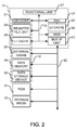
- FIG. 2 is a schematic diagram of a processing device, as shown in FIG. 1 .
- FIG. 3 shows an encoding scheme of a single-instruction-multiple-data (SIMD) vector compare-and-exchange instruction.
- SIMD single-instruction-multiple-data
- FIG. 4 is a block diagram of a first exemplar computer system for implementing the instruction format shown in FIG. 3 .
- FIG. 5 is block diagram of a second exemplar computer system for implementing the instruction format shown in FIG. 3 .
- FIG. 6 is a block diagram of a third exemplar computer system for implementing the instruction format shown in FIG. 3 .
- FIG. 7 is a block diagram of a fourth exemplar computer system for implementing the instruction format shown in FIG. 3 .
- One way to determine whether a semaphore is locked (and/or to make it so) is through the use of a read-modify-write sequence (or operation).
- a read-modify-write implementation is the acquisition and the release of the semaphore mechanism itself. That is, when a process attempts to gain control of the shared memory space, it first reads the lock value, check and modify (if permitted) the value and write the modifying value back to the lock. It is generally desirable to execute the read-modify-write operation as an atomic operation (i.e., completed without interruption once execution has begun) to prevent other processes from modifying the lock value.
- an atomic operation a process can acquire (read) the semaphore, modify the value (if permitted) and release the semaphore by initiating a write to complete the operation before another process attempts to acquire the lock.
- computer system 10 having a plurality of processing units 11 (e.g., processors, cores, execution units, etc.) coupled to a memory 12 (e.g., registers, cache, RAM, etc.) by a bus 13 .
- processing units 11 e.g., processors, cores, execution units, etc.
- memory 12 e.g., registers, cache, RAM, etc.
- One or more of the processing units 11 is associated with one or more threads.
- computer system 10 includes any suitable number of processing units 11 , each having any suitable number of threads.
- Processing units 11 may each form part of a separate integrated circuit device or, alternatively, all of the processing units 11 (or a portion thereof) may be formed on a single die.
- four processing units 11 are shown as part of system 10 . All four processing units 11 are coupled to memory 12 and specifically to a shared memory space 15 within memory 12 .
- memory 12 can be configured in a variety of ways. Although illustrated as a single memory, memory 12 may comprise multiple internal and/or external memories. In the particular example, all four processing units 11 access memory 12 , and a portion of memory 12 , designated as shared space 15 , is accessed by more than one processing unit 11 . It is possible that there may be other shared areas within memory 12 , in which two or more processing units 11 have the ability to access such shared areas. The non-shared areas of memory 12 are generally relegated to access by one processing unit 11 only.
- Computer system 10 illustrated in FIG. 1 is intended to be an exemplar computer system and may include many additional components, which have been omitted for clarity.
- the computer system 10 may include a DMA (direct memory access) controller, a network interface (e.g., a network card), a chip set associated with one or more of the processing units 11 , as well as additional signal lines and buses.
- DMA direct memory access
- network interface e.g., a network card
- chip set associated with one or more of the processing units 11
- additional signal lines and buses may be included in FIG. 1 .
- the semaphores employed are locks (or lock variables) 16 , which are assigned to control accesses to one or more respective shared spaces 15 (as shown by dotted-line 14 ).
- Lock 16 is a particular location in memory that is assigned to contain a value associated with obtaining access to the shared space 15 .
- it first accesses the corresponding lock 16 and test the state (value) of the data stored in lock location 16 .
- two values can be assigned to lock 16 . A first value indicating that the shared space is available for access and a second value indicating that the shared space is currently being utilized and, therefore, is not available for access.
- bit states 1 and 0 can be used for the locked and unlocked states for lock 16 .
- lock 16 is a design choice and many variations can be devised. Also, the location of lock 16 need not be within memory 12 itself. Furthermore, in reference to FIG. 1 , it is appreciated that memory 12 can be one of a variety of memory devices. It is also possible that one or more of processing units 11 can be replaced by a memory accessing device(s) (devices such as direct memory access controllers), which also access(es) the memory. In these instances, these devices would function similar to processing units 11 described herein for gaining access to shared space 15 . Finally, although only a single bus 13 is shown, there may be a plurality of buses at the same or different hierarchical level(s) as bus 13 for coupling the various devices.
- the accessing of memory 12 by processing units 11 for data transfer typically involves the use of load and store operations.
- the load operation transfers memory content from a location in memory accessed and the store operation transfers data to a memory location accessed.
- load/store operations are used to access the memory 12 and lock 16 for data transfer between processing units 11 and memory 12 .
- the load and store accesses are also referred to as read and write accesses, respectively.
- computer system 10 includes a read-only memory (ROM) 31 and a main memory 18 coupled—via system bus 22 —with processing units 11 , main memory 18 comprising, for example, any suitable type of random access memory (RAM).
- processing units 11 also have a data storage device 30 coupled therewith by system bus 22 .
- Data storage device 30 comprises any suitable non-volatile memory, such as, for example, a hard disk drive.
- Computer system 10 further includes a removable storage media 32 , such as a floppy disk drive, a CD ROM drive, and/or a USB Drive.
- processing unit 11 includes a number of components that are interconnected by one or more buses, and these buses are illustrated symbolically in FIG. 2 by a local bus 19 .
- Local bus 19 and, hence, the components of processing unit 11 —are coupled with a bus interface unit 23 .
- Bus interface unit 23 couples processing unit 11 with system bus 22 , thereby enabling communication between processing unit 11 and main memory 18 , as well as between processing unit 11 and an external cache 20 .
- Processing unit 11 includes an instruction decoder 21 coupled with local bus 19 .
- Instruction decoder 21 receives an instruction (or instructions) associated with a program or piece of code executing on processing unit 11 and breaks the instruction down into one or more machine-level instructions/operations (uops). It should be understood that processing unit 11 may receive one or more instructions associated with a program, whereas another processing unit 11 of computer system 10 may receive one or more instructions associated with the same program. Accordingly, a program may be executing on multiple processing units 11 .
- Processing unit 11 further includes multiple execution units, including, for example, data access control unit (DAC) 24 , memory-ordering buffer (MOB) 26 , a register file unit 29 , and functional unit 27 .
- DAC data access control unit
- MOB memory-ordering buffer
- Register file unit 29 includes a plurality of registers, each having 16, 32, 64, 128, 256, or 512 bits of storage. Further, register file 29 may include one or more register files, each having one or more registers.
- Functional unit 27 comprises one or more functional units, such as, for example, an arithmetic, logic, and/or floating-point unit. MOB 26 ensures the proper ordering of load and store instructions and, further, provides for the proper sequencing of these transactions within the memory hierarchy (i.e., the various levels of memory within computer system 10 , including L0 cache 25 , L1 cache 28 , external cache 20 , main memory 18 , and data storage device 30 ).
- Each of the L0 cache 25 and L1 cache 28 can store data recently accessed, or expected to be accessed, by functional unit 27 . If an item of data requested by functional unit 27 is resident in one of cache memories 25 , 28 , a cache “hit” has occurred; however, if the requested data is not present in cache, then a cache “miss” has occurred.
- One or more of the cache memories e.g., L0 cache 25
- DAC 24 controls all transactions that resulted in a cache miss, as well as other transactions that require special handling.
- a lock is one type of transaction that requires special handling by the DAC 24 and by other components of processing unit 11 .
- a uop corresponds to, for example, an arithmetic operation, that uop is dispatched to functional unit 27 , which then performs the arithmetic operation. If a uop corresponds to a memory-referencing instruction—e.g., a load or a store—that uop is dispatched to MOB 26 .
- a memory-referencing instruction e.g., a load or a store
- processing unit 11 illustrated in FIG. 2 is intended to represent an exemplar processing device and, further, that such a processing unit may include many additional components that are not shown in these figures. These components having been omitted for ease of understanding.
- the processing unit 11 may include an address generation unit, a reservation station, reorder buffer, scheduler, a segmentation and address translation unit, a translation lookaside buffer, a page miss handler, and/or internal clock circuitry.
- the processing unit 11 may include an address generation unit, a reservation station, reorder buffer, scheduler, a segmentation and address translation unit, a translation lookaside buffer, a page miss handler, and/or internal clock circuitry.
- FIG. 2 may be combined and/or share circuitry.
- Any one or more of the uops scheduled for execution may comprise a locked uop.
- the lock corresponds to a sequence of operations (e.g., load, modify, and store) that are performed in a manner that insures synchronization between processors and/or threads.
- FIG. 3 shows an instruction for performing a read-modify-write operation.
- Instruction 40 is a single atomic instruction including five operands 41 - 45 .
- Opcode operand 41 identifies that this is a VCMPXCHG instruction.
- Operands 42 - 44 correspond to the source and destination operands associated with SRC1/DEST, SRC2, SRC3, and, in some implementations, a mask storage location (MSK) and/or an offset (or “immediate”) operand 45 .
- This offset or immediate is used to provide for an offset from a base address (such as SRC1) when addressing memory 12 .
- the instructions noted below may have such offsets, but are not illustrated.
- Implementations specifying a mask storage location 45 reference a register or memory location that stores mask elements corresponding to respective data elements stored at the storage location referenced by the SRC1/DEST operand.
- processing unit 11 reads a first source data, compares it to another source data and if the comparison meets a predesignated condition (such as a true or match condition), some modified value is written to a location, which may be the original location of the first source data. If the predesignated condition is not met, the original data in the location is not changed.
- the instruction utilizes three source operands (such as SRC1, SRC2 and SRC3, as used hereinafter) and one destination operand (such as DEST, as used hereinafter) to supply the location of the various information used in executing the instruction.
- Operation-specific registers may be used for providing one or more of the source data and/or for storing the destination data when the instruction is executed, eliminating the need to specify the operands explicitly in the actual instruction format.
- the SRC1 operand and the DEST operand refer to the same storage location (SRC1/DEST).
- SRC1, SRC2 and SRC3 are loaded into registers in register file unit 29 .
- the value is initially read into a location specified by the SRC2 operand, and a replacement value is read into a location specified by the SRC3 operand.
- an atomic compare-exchange operation is executed to compare the present value associated with the SRC1/DEST operand to the value associated with the SRC2 operand (i.e., the present value may be different from the initially copied value due to modification by another agent).
- the value has not changed, it is replaced with the value associated with the SRC3 operand, and the zero flag is set to indicate a successful update. However, if another agent has modified the value between the initial copy and the compare-exchange operation, the current value is not replaced and the zero flag is cleared to indicate a failed update.
- the block diagram of FIG. 4 illustrates the information flow when instruction 40 is executed.
- the processing unit 11 includes an execution unit 46 (e.g., DAC 24 of FIG. 2 ), register file 29 , BIU 23 , and decoder 21 , which are all coupled together by local bus 19 .
- Register file 29 includes a plurality of registers which are accessed by execution unit 46 for executing the various operations.
- the VCMPXCHG instruction 40 is shown resident within execution unit 46 and dotted lines are shown from the operands of the instruction to the corresponding registers associated with SRC1, SRC2, SRC3 and DEST.
- the registers reside within register file 29 .
- Decoder 21 is used to decode the various instructions (including VCMPXCHG instruction 40 ), in order for execution unit 46 to perform the operations.
- Memory 12 is shown coupled to BIU 23 by bus 19 and/or bus 22 . Accordingly, data transfers between processing unit 11 and memory 12 may occur through BIU 54 a or local bus 19 . It is to be appreciated that the program routine utilizing the VCMPXCHG instruction 40 may reside within some memory, which could also be or include memory 12 .
- the following pseudo-code illustrates examples of how the VCMPXCHG instruction 40 operates.
- Other pseudo-code, languages, operations, orders of operations, and/or numbers may be used.
- lock values are stored in bits [127:0] and bits [255:0], respectively, of a 512-bit storage location referenced by SRC1/DEST (e.g., a 64 byte cache line or register).
- SRC1/DEST may reference sixteen 8-bit lock values (128 bits), each corresponding to a respective one of sixteen storage locations in a cache line or SIMD register.
- SRC1/DEST may reference thirty-two 8-bit lock values (256 bits), each corresponding to a respective one of thirty-two storage locations in a cache line or SIMD register.
- the result of the comparison between SRC1/DEST and SRC2 indicates whether the lock values have been modified.
- a true condition indicates the locks have not been modified and that the locks are in the unlocked state.
- the values referenced by SRC3 are written to SRC1/DEST, modifying the lock values to a locked state, in order to prevent other agents from having access to the shared space(s). Thereafter, the zero flag (ZF) is set to indicate a successful operation.
- a false condition indicates one or more of the locks have been modified (locked) and that another agent has taken ownership of the shared space.
- the values referenced by SRC1/DEST (the current lock values) are stored to SRC2, and the zero flag is cleared to indicate an unsuccessful operation. The upper bytes of SRC2 are then cleared prior to returning from the operation.
- an outer loop will include a non-atomic load and test prior to re-executing VCMPXCHG instruction 40 .
- the processor Once the processor completes its access(es) to the shared memory space 15 , it will typically release its control over the shared memory space 15 with a write cycle to lock 16 to unlock it, so that other agents can now gain entry into shared memory space 15 .
- how the processor releases the shared memory space is a design choice, which could be dictated by the system architecture.
- VCMPXCHG instruction 40 includes a mask vector having multiple mask elements, each corresponding to one of a plurality of data elements referenced by SRC1/DEST.
- the mask vector storage location may be a register in a register file unit 29 , such as, for example, a shadow register, a control register, a flag register, a general purpose register, a SIMD register, or other appropriate register.
- Mask elements or values may include flags, markers, tabs, indicators, and or other numbers, bits and/or codes for indicating whether a corresponding data element (e.g., in a corresponding or pointed register location) is to be compared and/or modified. For example, a mask element having a value of “1” may indicate that a corresponding data element is to be modified; otherwise a “0” may be used. Other numbers or flags may be used.
- Examples of masked VCMPXCHGD and VCMPXCHGQ instructions are illustrated in pseudo-code below for a 16 wide, 512 byte vector and an 8 wide, 512 byte vector, respectively. In the masked compare implementations, only the active elements are compared and updated.
- a variable, ALL_CMPS_SUCCEED is first preset to 1 (i.e., a true condition).
- the corresponding storage location referenced by SRC1/DEST is compared to the value referenced by corresponding bits in SRC2. If no mask is used, each of the storage locations referenced by SRC1/DEST is compared to the value referenced by corresponding bits in SRC2.
- the result of the comparison between corresponding values of SRC1/DEST and SRC2 indicates whether that particular lock value has been modified.
- a true condition i.e. a non-matching condition
- ALL_CMPS_SUCCEED is cleared, indicating that all comparisons did not succeed. Thereafter, the zero flag is cleared and for each active mask element, the value stored in the corresponding storage location referenced by SRC1/DEST is loaded into corresponding bits in SRC2.
- ALL_CMPS_SUCCEED remains set without change. Thereafter, the zero flag (ZF) is set and for each active mask element, the value stored in the corresponding storage location in SRC3 is loaded into corresponding bits in SRC1/DEST, modifying the lock values to a locked state, in order to prevent other agents from having access to the shared spaces.
- ZF zero flag
- FIG. 5 illustrates another example of the information flow when instruction 40 is executed.
- the VCMPXCHG instruction 40 is shown resident within execution unit 46 and dotted lines are shown from the operands of the instruction to the corresponding registers associated with SRC2, SRC3, and MSK.
- the mask storage location (MSK) is a mask register and the storage location associated with SRC1/DEST is an L1 cache.
- the registers reside within register file unit 29 .
- SRC1 Prior to the execution of instruction 40 , SRC1 is prefetched into the L1 cache and SRC2, SRC3, and MSK data are loaded into the registers in register file unit 29 .
- the mask register stores a plurality of mask elements corresponding to respective data elements in the storage location associated with the SRC1/DEST operand.
- a comparison value is initially read into a location specified by the SRC2 operand, and a replacement value is read into a location specified by the SRC3 operand.
- instruction 40 is executed to cause execution unit 46 to compare corresponding data elements associated with the SRC1/DEST and SRC2 operands, and if a match exists, to replace data elements from SRC1/DEST with corresponding data elements from SRC3. If a match does not exist, execution of the instruction 40 causes execution unit 46 to replace SRC2 data elements with corresponding SRC1/DEST data elements.
- the comparison between pairs of SRC1/DEST and SRC2 data elements is only performed if a corresponding mask element is active.
- execution unit 46 is further configured to set a flag if a match exists between each pair of corresponding data elements for which a corresponding mask element is active and to clear the flag if a match does not exist between any of the of the pairs for which a corresponding mask element is active.
- replacement of the SRC1/DEST data elements by corresponding SRC3 data elements is only performed if a mask element corresponding to the respective SRC1/DEST data element is active.
- replacement of the SRC2 data element by a corresponding SRC1/DEST data element is only performed if a mask element corresponding to the SRC1/DEST data element is active.
- the lock value indicating a locked condition is the same as the mask value indicating an active mask element (e.g., a binary 1).
- SRC3 may be used as both a mask vector and a lock value replacement vector.
- the compare-exchange operation completes execution without updating the value associated with the SRC2 operand. Thereafter, a flag (e.g., the zero flag) is tested and if it indicates the update operation failed with respect to the value associated with the SRC1/DEST operand, the steps just prior to the compare-exchange operation are repeated to update values associated with SRC2 and SRC3 prior to repeating the compare-exchange operation.
- a flag e.g., the zero flag
- One or more embodiments include an article of manufacture that includes a tangible machine-accessible and/or machine-readable medium having stored thereon a SIMD instruction specifying a vector compare-and-exchange operation for a plurality of data elements, each data element having a corresponding test element, replacement element, and mask element, that if executed by a machine (e.g., an execution unit) causes the machine to compare data elements to corresponding test elements if respective mask elements are active; and responsive to determining all comparisons indicate a match, set a flag and replace compared data elements with corresponding replacement elements; and responsive to determining all comparisons do not indication a match, clear a flag and replace compared test elements with corresponding data elements.
- the tangible medium may include one or more solid materials.
- the medium may include, a mechanism that provides, for example stores, information in a form that is accessible by the machine.
- the medium may optionally include recordable mediums, such as, for example, floppy diskette, optical storage medium, optical disk, CD-ROM, magnetic disk, magneto-optical disk, read only memory (ROM), programmable ROM (PROM), erasable-and-programmable ROM (EPROM), electrically-erasable-and-programmable ROM (EEPROM), random access memory (RAM), static-RAM (SRAM), dynamic-RAM (DRAM), Flash memory, and combinations thereof.
- recordable mediums such as, for example, floppy diskette, optical storage medium, optical disk, CD-ROM, magnetic disk, magneto-optical disk, read only memory (ROM), programmable ROM (PROM), erasable-and-programmable ROM (EPROM), electrically-erasable-and-programmable ROM (EEPROM), random access memory (RAM), static-RAM (SRAM), dynamic-RAM (DRAM), Flash
- Suitable machines include, but are not limited to, execution units, general-purpose processors, special-purpose processors (e.g., graphics processors and cryptographic processors), cryptographic accelerators, network communications processors, computer systems, network devices, modems, personal digital assistants (PDAs), cellular phones, and a wide variety of other electronic devices with one or more execution units, to name just a few examples. Still other embodiments pertain to a computer system, embedded system, or other electronic device having an execution unit and/or performing a method as disclosed herein.
- FIG. 6 illustrates an example of a suitable computer system 50 including a processor 51 .
- the processor includes at least one execution unit 52 that is capable of executing at least one vector compare-and-exchange instruction 53 .
- the processor is coupled to a chipset 54 via a bus (e.g., a front side bus) or other interconnect 55 .
- the interconnect may be used to transmit data signals between the processor and other components in the system via the chipset.
- the chipset includes a system logic chip known as a memory controller hub (MCH) 56 .
- the MCH is coupled to the front side bus or other interconnect 55 .
- a memory 58 is coupled to the MCH.
- the memory may include a random access memory (RAM).
- RAM random access memory
- DRAM is an example of a type of RAM used in some but not all computer systems.
- the memory may be used to store instructions 59 , such as one or more multiply instructions, and data 60 .
- a component interconnect 61 is also coupled with the MCH.
- the component interconnect may include one or more peripheral component interconnect express (PCIe) interfaces.
- PCIe peripheral component interconnect express
- the component interconnect may allow other components to be coupled to the rest of the system through the chipset.
- One example of such components is a graphics chip or other graphics device, although this is optional and not required.
- the chipset also includes an input/output (I/O) controller hub (ICH) 62 .
- the ICH is coupled to the MCH through hub interface bus or other interconnect 63 .
- the bus or other interconnect 63 may include a Direct Media Interface (DMI).
- DMI Direct Media Interface
- a data storage 64 is coupled to the ICH.
- the data storage may include a hard disk drive, a floppy disk drive, a CD-ROM device, a flash memory device, or the like, or a combination thereof.
- a second component interconnect 65 is also coupled with the ICH.
- the second component interconnect may include one or more peripheral component interconnect express (PCIe) interfaces.
- PCIe peripheral component interconnect express
- the second component interconnect may allow various types of components to be coupled to the rest of the system through the chipset.
- a serial expansion port 66 is also coupled with the ICH.
- the serial expansion port may include one or more universal serial bus (USB) ports.
- USB universal serial bus
- the serial expansion port may allow various other types of input/output devices to be coupled to the rest of the system through the chipset.
- ICH ICH
- other components that may optionally be coupled with the ICH include, but are not limited to, an audio controller, a wireless transceiver, and a user input device (e.g., a keyboard, mouse).
- a user input device e.g., a keyboard, mouse
- a network controller 67 is also coupled to the ICH.
- the network controller may allow the system to be coupled with a network.
- the computer system may execute a version of the WINDOWSTM operating system, available from Microsoft Corporation of Redmond, Wash.
- WINDOWSTM operating system available from Microsoft Corporation of Redmond, Wash.
- other operating systems such as, for example, UNIX, Linux, or embedded systems, may be used.
- the processor may have multiple cores.
- the MCH 56 may be physically integrated on-die with the processor 51 and the processor may be directly coupled with a memory 58 through the integrated MCH.
- other components may be integrated on-die with the processor, such as to provide a system-on-chip (SoC) design.
- SoC system-on-chip
- the computer system may have multiple processors.
- FIG. 7 is another example of a suitable computer system 70 .
- the second example embodiment has certain similarities to computer system 50 described above. For clarity, the discussion will tend to emphasize the differences without repeating all of the similarities.
- computer system 70 includes a processor 71 , and a chipset 74 having an I/O controller hub (ICH) 72 .
- Computer system 70 also includes a first component interconnect 81 coupled with chipset 74 , a second component interconnect 85 coupled with the ICH, a serial expansion port 86 coupled with the ICH, a network controller 87 coupled with the ICH, and a data storage 84 coupled with the ICH.
- ICH I/O controller hub
- Processor 71 is a multi-core processor and includes processor cores 72 - 1 through 72 -M, where M may be an integer number equal to or larger than two (e.g. two, four, seven, or more). Each core may include at least one execution unit that is capable of executing at least one embodiment of an instruction as disclosed herein. As shown, the core-1 includes a cache 88 (e.g., an L1 cache). Each of the other cores may similarly include a dedicated cache.
- the processor cores may be implemented on a single integrated circuit (IC) chip.
- the processor also includes at least one shared cache 89 .
- the shared cache may store data (e.g., instructions) that are utilized by one or more components of the processor, such as the cores.
- the shared cache may locally cache data stored in a memory 78 for faster access by components of the processor.
- the shared cache may include one or more mid-level caches, such as level 2 (L2), level 3 (L3), level 4 (L4), or other levels of cache, a last level cache (LLC), and/or combinations thereof.
- LLC last level cache
- the processor cores and the shared cache are each coupled with a bus or other interconnect 90 .
- the bus or other interconnect may couple the cores and the shared cache and allow communication.
- the processor also includes a memory controller hub (MCH) 76 .
- MCH memory controller hub
- the MCH is integrated with the processor 71 .
- the MCH may be on-die with the processor cores.
- the processor is coupled with the memory 78 through the MCH.
- the memory may include DRAM, although this is not required.
- the chipset includes an input/output (I/O) hub 91 .
- the I/O hub is coupled with the processor through a bus (e.g., a QuickPath Interconnect (QPI)) or other interconnect 75 .
- the first component interconnect 81 is coupled with the I/O hub 91 .
- Certain operations may be performed by hardware components, or may be embodied in machine-executable instructions, that may be used to cause, or at least result in, a circuit or hardware programmed with the instructions performing the operations.
- the circuit may include a general-purpose or special-purpose processor, or logic circuit, to name just a few examples.
- the operations may also optionally be performed by a combination of hardware and software.
- An execution unit and/or a processor may include specific or particular circuitry or other logic responsive to a machine instruction or one or more control signals derived from the machine instruction to store an instruction specified result operand.
- the access controls to shared areas of the memory can be achieved by means other than the test-and-set sequence described in the example above.
- a simple counter can be used in which each access is incremented by a specified count.
- the VCMPXCHG instruction of the preferred embodiment performs the read-modify-write operation, but that the modifying and writing phases are achieved essentially as a single step.
- the modifying values of the VCMPXCHG instruction are preset for use by the instruction. Although their use is dependent on the decision obtained when the comparison is made, this preset modifying values (SRC3) may be written immediately to the destination to modify the destination value.
- the VCMPXCHG instructions and implementations described herein can be utilized in other capacities as well and need not be limited to the function of controlling the access to a shared memory space.
- the VCMPXCHG instructions may be used for speculative execution in which a SIMD operation is performed on a plurality of data elements, the results of which are only written to the shared memory space if the data elements have not been modified by another agent during the operation. Accordingly, other embodiments are within the scope of the following claims.
Landscapes
- Engineering & Computer Science (AREA)
- Theoretical Computer Science (AREA)
- Software Systems (AREA)
- Physics & Mathematics (AREA)
- General Engineering & Computer Science (AREA)
- General Physics & Mathematics (AREA)
- Mathematical Physics (AREA)
- Computer Hardware Design (AREA)
- Computing Systems (AREA)
- Memory System Of A Hierarchy Structure (AREA)
- Complex Calculations (AREA)
- Advance Control (AREA)
- Multi Processors (AREA)
Priority Applications (12)
| Application Number | Priority Date | Filing Date | Title |
|---|---|---|---|
| US12/644,529 US8996845B2 (en) | 2009-12-22 | 2009-12-22 | Vector compare-and-exchange operation |
| TW102143765A TWI525539B (zh) | 2009-12-22 | 2010-11-11 | 用於同步化simd向量的方法,處理器,及系統 |
| TW099138849A TWI427533B (zh) | 2009-12-22 | 2010-11-11 | 用於同步化simd向量的方法,處理器,及系統 |
| DE112010004963T DE112010004963T5 (de) | 2009-12-22 | 2010-11-29 | Synchronisieren von SIMD Vektoren |
| GB1119083.2A GB2488619B (en) | 2009-12-22 | 2010-11-29 | Synchronizing SIMD vectors |
| JP2012517936A JP5421458B2 (ja) | 2009-12-22 | 2010-11-29 | Simdベクトルの同期 |
| KR1020127019177A KR101461378B1 (ko) | 2009-12-22 | 2010-11-29 | 동기화 simd 벡터 |
| PCT/US2010/058238 WO2011087590A2 (en) | 2009-12-22 | 2010-11-29 | Synchronizing simd vectors |
| CN201510434397.XA CN105094749A (zh) | 2009-12-22 | 2010-12-21 | Simd向量的同步化 |
| CN201010619577.2A CN102103570B (zh) | 2009-12-22 | 2010-12-21 | Simd向量的同步化 |
| BRPI1005259-3A BRPI1005259A2 (pt) | 2009-12-22 | 2010-12-22 | vetores simd sincronizadores |
| JP2013240725A JP5876458B2 (ja) | 2009-12-22 | 2013-11-21 | Simdベクトルの同期 |
Applications Claiming Priority (1)
| Application Number | Priority Date | Filing Date | Title |
|---|---|---|---|
| US12/644,529 US8996845B2 (en) | 2009-12-22 | 2009-12-22 | Vector compare-and-exchange operation |
Publications (2)
| Publication Number | Publication Date |
|---|---|
| US20110153989A1 US20110153989A1 (en) | 2011-06-23 |
| US8996845B2 true US8996845B2 (en) | 2015-03-31 |
Family
ID=44152784
Family Applications (1)
| Application Number | Title | Priority Date | Filing Date |
|---|---|---|---|
| US12/644,529 Expired - Fee Related US8996845B2 (en) | 2009-12-22 | 2009-12-22 | Vector compare-and-exchange operation |
Country Status (9)
| Country | Link |
|---|---|
| US (1) | US8996845B2 (de) |
| JP (2) | JP5421458B2 (de) |
| KR (1) | KR101461378B1 (de) |
| CN (2) | CN105094749A (de) |
| BR (1) | BRPI1005259A2 (de) |
| DE (1) | DE112010004963T5 (de) |
| GB (1) | GB2488619B (de) |
| TW (2) | TWI525539B (de) |
| WO (1) | WO2011087590A2 (de) |
Families Citing this family (56)
| Publication number | Priority date | Publication date | Assignee | Title |
|---|---|---|---|---|
| US9672019B2 (en) | 2008-11-24 | 2017-06-06 | Intel Corporation | Systems, apparatuses, and methods for a hardware and software system to automatically decompose a program to multiple parallel threads |
| US10621092B2 (en) | 2008-11-24 | 2020-04-14 | Intel Corporation | Merging level cache and data cache units having indicator bits related to speculative execution |
| US8996845B2 (en) | 2009-12-22 | 2015-03-31 | Intel Corporation | Vector compare-and-exchange operation |
| US9417855B2 (en) | 2011-09-30 | 2016-08-16 | Intel Corporation | Instruction and logic to perform dynamic binary translation |
| CN103959237B (zh) * | 2011-11-30 | 2016-09-28 | 英特尔公司 | 用于提供向量横向比较功能的指令和逻辑 |
| US10318291B2 (en) | 2011-11-30 | 2019-06-11 | Intel Corporation | Providing vector horizontal compare functionality within a vector register |
| CN104011657B (zh) * | 2011-12-22 | 2016-10-12 | 英特尔公司 | 用于向量计算和累计的装置和方法 |
| CN104081342B (zh) | 2011-12-23 | 2017-06-27 | 英特尔公司 | 经改进的插入指令的装置和方法 |
| WO2013095637A1 (en) | 2011-12-23 | 2013-06-27 | Intel Corporation | Apparatus and method of improved permute instructions |
| CN104081341B (zh) | 2011-12-23 | 2017-10-27 | 英特尔公司 | 用于多维数组中的元素偏移量计算的指令 |
| US9588764B2 (en) | 2011-12-23 | 2017-03-07 | Intel Corporation | Apparatus and method of improved extract instructions |
| CN107220029B (zh) | 2011-12-23 | 2020-10-27 | 英特尔公司 | 掩码置换指令的装置和方法 |
| US20140223138A1 (en) * | 2011-12-23 | 2014-08-07 | Elmoustapha Ould-Ahmed-Vall | Systems, apparatuses, and methods for performing conversion of a mask register into a vector register. |
| CN104040487B (zh) * | 2011-12-23 | 2017-10-13 | 英特尔公司 | 用于合并掩码模式的指令 |
| US9489196B2 (en) | 2011-12-23 | 2016-11-08 | Intel Corporation | Multi-element instruction with different read and write masks |
| US9946540B2 (en) | 2011-12-23 | 2018-04-17 | Intel Corporation | Apparatus and method of improved permute instructions with multiple granularities |
| CN107092465B (zh) * | 2011-12-23 | 2021-06-29 | 英特尔公司 | 用于提供向量混合和置换功能的指令和逻辑 |
| CN104067224B (zh) | 2011-12-23 | 2017-05-17 | 英特尔公司 | 在不同的粒度水平下对数据值进行广播和掩码的指令执行 |
| CN104011649B (zh) * | 2011-12-23 | 2018-10-09 | 英特尔公司 | 用于在simd/向量执行中传播有条件估算值的装置和方法 |
| US9552313B2 (en) | 2011-12-28 | 2017-01-24 | Intel Corporation | Delivering real time interrupts with an advanced programmable interrupt controller |
| WO2013100996A1 (en) * | 2011-12-28 | 2013-07-04 | Intel Corporation | Binary translation in asymmetric multiprocessor system |
| US20150134932A1 (en) * | 2011-12-30 | 2015-05-14 | Cameron B. McNairy | Structure access processors, methods, systems, and instructions |
| US9575753B2 (en) * | 2012-03-15 | 2017-02-21 | International Business Machines Corporation | SIMD compare instruction using permute logic for distributed register files |
| US9405538B2 (en) | 2012-12-28 | 2016-08-02 | Intel Corporation | Functional unit having tree structure to support vector sorting algorithm and other algorithms |
| WO2014137327A1 (en) * | 2013-03-05 | 2014-09-12 | Intel Corporation | Analyzing potential benefits of vectorization |
| US9411593B2 (en) * | 2013-03-15 | 2016-08-09 | Intel Corporation | Processors, methods, systems, and instructions to consolidate unmasked elements of operation masks |
| US9405937B2 (en) | 2013-06-28 | 2016-08-02 | Intel Corporation | Method and apparatus for securing a dynamic binary translation system |
| US9292298B2 (en) * | 2013-07-08 | 2016-03-22 | Arm Limited | Data processing apparatus having SIMD processing circuitry |
| US9495155B2 (en) | 2013-08-06 | 2016-11-15 | Intel Corporation | Methods, apparatus, instructions and logic to provide population count functionality for genome sequencing and alignment |
| US11257271B2 (en) | 2013-09-26 | 2022-02-22 | Imagination Technologies Limited | Atomic memory update unit and methods |
| GB2520603B (en) * | 2013-09-26 | 2016-04-06 | Imagination Tech Ltd | Atomic memory update unit and methods |
| US9466091B2 (en) | 2013-09-26 | 2016-10-11 | Imagination Technologies Limited | Atomic memory update unit and methods |
| US9891936B2 (en) | 2013-09-27 | 2018-02-13 | Intel Corporation | Method and apparatus for page-level monitoring |
| US9390023B2 (en) * | 2013-10-03 | 2016-07-12 | Cavium, Inc. | Method and apparatus for conditional storing of data using a compare-and-swap based approach |
| US10445092B2 (en) * | 2014-12-27 | 2019-10-15 | Intel Corporation | Method and apparatus for performing a vector permute with an index and an immediate |
| US9996350B2 (en) | 2014-12-27 | 2018-06-12 | Intel Corporation | Hardware apparatuses and methods to prefetch a multidimensional block of elements from a multidimensional array |
| US10528345B2 (en) * | 2015-03-27 | 2020-01-07 | Intel Corporation | Instructions and logic to provide atomic range modification operations |
| US10019264B2 (en) * | 2016-02-24 | 2018-07-10 | Intel Corporation | System and method for contextual vectorization of instructions at runtime |
| GB2549737B (en) * | 2016-04-26 | 2019-05-08 | Advanced Risc Mach Ltd | An apparatus and method for managing address collisions when performing vector operations |
| WO2018022525A1 (en) * | 2016-07-27 | 2018-02-01 | Intel Corporation | System and method for multiplexing vector mask matches |
| US20190155603A1 (en) * | 2016-07-27 | 2019-05-23 | Intel Corporation | System and method for multiplexing vector compare |
| EP3336691B1 (de) | 2016-12-13 | 2022-04-06 | ARM Limited | Replikatelementanweisung |
| EP3336692B1 (de) | 2016-12-13 | 2020-04-29 | Arm Ltd | Replikatpartitionsanweisung |
| CN107895191B (zh) | 2017-10-30 | 2022-02-22 | 上海寒武纪信息科技有限公司 | 一种信息处理方法及相关产品 |
| US20210133854A1 (en) | 2018-09-13 | 2021-05-06 | Shanghai Cambricon Information Technology Co., Ltd. | Information processing method and terminal device |
| CN111258637B (zh) * | 2018-11-30 | 2022-08-05 | 上海寒武纪信息科技有限公司 | 数据处理方法、处理器、数据处理装置及存储介质 |
| CN111258640B (zh) * | 2018-11-30 | 2022-10-04 | 上海寒武纪信息科技有限公司 | 数据处理方法、处理器、数据处理装置及存储介质 |
| CN111258639B (zh) * | 2018-11-30 | 2022-10-04 | 上海寒武纪信息科技有限公司 | 数据处理方法、处理器、数据处理装置及存储介质 |
| CN111258638B (zh) * | 2018-11-30 | 2022-10-04 | 上海寒武纪信息科技有限公司 | 数据处理方法、处理器、数据处理装置及存储介质 |
| CN111258642B (zh) * | 2018-11-30 | 2022-10-04 | 上海寒武纪信息科技有限公司 | 数据处理方法、处理器、数据处理装置及存储介质 |
| US20200210181A1 (en) * | 2018-12-29 | 2020-07-02 | Intel Corporation | Apparatuses, methods, and systems for vector element sorting instructions |
| US20200401412A1 (en) * | 2019-06-24 | 2020-12-24 | Intel Corporation | Hardware support for dual-memory atomic operations |
| CN110515660B (zh) * | 2019-08-28 | 2021-08-06 | 中国人民解放军国防科技大学 | 一种加速原子指令执行的方法和装置 |
| CN110515659B (zh) * | 2019-08-28 | 2021-10-01 | 中国人民解放军国防科技大学 | 一种原子指令的执行方法和装置 |
| WO2022266842A1 (zh) * | 2021-06-22 | 2022-12-29 | 华为技术有限公司 | 一种多线程数据处理方法及装置 |
| CN115098165B (zh) * | 2022-06-13 | 2023-09-08 | 昆仑芯(北京)科技有限公司 | 数据处理方法、装置、芯片、设备及介质 |
Citations (10)
| Publication number | Priority date | Publication date | Assignee | Title |
|---|---|---|---|---|
| JPS6285372A (ja) | 1985-10-09 | 1987-04-18 | Nec Corp | マルチプロセツサシステムにおけるコンペアアンドスワツプ方式 |
| US6460121B1 (en) * | 1998-09-14 | 2002-10-01 | Compaq Information Technologies Group, L.P. | Method for providing an atomic memory read using a compare-exchange instruction primitive |
| US20020147872A1 (en) | 2001-04-09 | 2002-10-10 | Sun Microsystems, Inc. | Sequentially performed compound compare-and-swap |
| US20030069913A1 (en) | 2001-10-05 | 2003-04-10 | Deli Deng | Multiply-accumulate (MAC) unit for single-instruction/multiple-data (SIMD) instructions |
| US20040078554A1 (en) | 2000-02-29 | 2004-04-22 | International Business Machines Corporation | Digital signal processor with cascaded SIMD organization |
| CN1790310A (zh) | 2004-12-17 | 2006-06-21 | 英特尔公司 | 用于单指令、多数据执行引擎标志寄存器的评估单元 |
| JP2007157142A (ja) | 2005-12-01 | 2007-06-21 | Sony Computer Entertainment Inc | 特定のspeを使ってcellプロセッサのアトミックなコンペア・アンド・スワップ命令を実行するための技術 |
| US20070260634A1 (en) | 2006-05-04 | 2007-11-08 | Nokia Corporation | Apparatus, system, method, and computer program product for synchronizing the presentation of media content |
| US7627723B1 (en) | 2006-09-21 | 2009-12-01 | Nvidia Corporation | Atomic memory operators in a parallel processor |
| WO2011087590A2 (en) | 2009-12-22 | 2011-07-21 | Intel Corporation | Synchronizing simd vectors |
Family Cites Families (5)
| Publication number | Priority date | Publication date | Assignee | Title |
|---|---|---|---|---|
| US4482956A (en) * | 1982-11-04 | 1984-11-13 | International Business Machines Corporation | Parallel queueing method |
| JPS61288243A (ja) * | 1985-06-17 | 1986-12-18 | Fujitsu Ltd | コンペアアンドスワツプ命令処理方式 |
| CN100545804C (zh) * | 2003-08-18 | 2009-09-30 | 上海海尔集成电路有限公司 | 一种基于cisc结构的微控制器及其指令集的实现方法 |
| US8607241B2 (en) * | 2004-06-30 | 2013-12-10 | Intel Corporation | Compare and exchange operation using sleep-wakeup mechanism |
| US7908255B2 (en) * | 2007-04-11 | 2011-03-15 | Microsoft Corporation | Transactional memory using buffered writes and enforced serialization order |
-
2009
- 2009-12-22 US US12/644,529 patent/US8996845B2/en not_active Expired - Fee Related
-
2010
- 2010-11-11 TW TW102143765A patent/TWI525539B/zh not_active IP Right Cessation
- 2010-11-11 TW TW099138849A patent/TWI427533B/zh not_active IP Right Cessation
- 2010-11-29 DE DE112010004963T patent/DE112010004963T5/de not_active Withdrawn
- 2010-11-29 KR KR1020127019177A patent/KR101461378B1/ko not_active IP Right Cessation
- 2010-11-29 WO PCT/US2010/058238 patent/WO2011087590A2/en active Application Filing
- 2010-11-29 GB GB1119083.2A patent/GB2488619B/en not_active Expired - Fee Related
- 2010-11-29 JP JP2012517936A patent/JP5421458B2/ja not_active Expired - Fee Related
- 2010-12-21 CN CN201510434397.XA patent/CN105094749A/zh active Pending
- 2010-12-21 CN CN201010619577.2A patent/CN102103570B/zh not_active Expired - Fee Related
- 2010-12-22 BR BRPI1005259-3A patent/BRPI1005259A2/pt not_active Application Discontinuation
-
2013
- 2013-11-21 JP JP2013240725A patent/JP5876458B2/ja not_active Expired - Fee Related
Patent Citations (16)
| Publication number | Priority date | Publication date | Assignee | Title |
|---|---|---|---|---|
| JPS6285372A (ja) | 1985-10-09 | 1987-04-18 | Nec Corp | マルチプロセツサシステムにおけるコンペアアンドスワツプ方式 |
| US6460121B1 (en) * | 1998-09-14 | 2002-10-01 | Compaq Information Technologies Group, L.P. | Method for providing an atomic memory read using a compare-exchange instruction primitive |
| US20040078554A1 (en) | 2000-02-29 | 2004-04-22 | International Business Machines Corporation | Digital signal processor with cascaded SIMD organization |
| US20020147872A1 (en) | 2001-04-09 | 2002-10-10 | Sun Microsystems, Inc. | Sequentially performed compound compare-and-swap |
| US20030069913A1 (en) | 2001-10-05 | 2003-04-10 | Deli Deng | Multiply-accumulate (MAC) unit for single-instruction/multiple-data (SIMD) instructions |
| CN1633637A (zh) | 2001-10-05 | 2005-06-29 | 英特尔公司 | 用于单指令/多数据指令的乘法积累单元 |
| CN1662904A (zh) | 2002-06-26 | 2005-08-31 | 国际商业机器公司 | 具有级联simd结构的数字信号处理器 |
| WO2006066262A2 (en) | 2004-12-17 | 2006-06-22 | Intel Corporation | Evalutation unit for single instruction, multiple data execution engine flag registers |
| CN1790310A (zh) | 2004-12-17 | 2006-06-21 | 英特尔公司 | 用于单指令、多数据执行引擎标志寄存器的评估单元 |
| US20060149924A1 (en) | 2004-12-17 | 2006-07-06 | Dwyer Michael K | Evaluation unit for single instruction, multiple data execution engine flag registers |
| TWI297853B (en) | 2004-12-17 | 2008-06-11 | Intel Corp | Method for performing in a simd execution engine, apparatus for a simd execution engine, and processing system |
| JP2007157142A (ja) | 2005-12-01 | 2007-06-21 | Sony Computer Entertainment Inc | 特定のspeを使ってcellプロセッサのアトミックなコンペア・アンド・スワップ命令を実行するための技術 |
| US20070143551A1 (en) * | 2005-12-01 | 2007-06-21 | Sony Computer Entertainment Inc. | Cell processor atomic compare and swap using dedicated SPE |
| US20070260634A1 (en) | 2006-05-04 | 2007-11-08 | Nokia Corporation | Apparatus, system, method, and computer program product for synchronizing the presentation of media content |
| US7627723B1 (en) | 2006-09-21 | 2009-12-01 | Nvidia Corporation | Atomic memory operators in a parallel processor |
| WO2011087590A2 (en) | 2009-12-22 | 2011-07-21 | Intel Corporation | Synchronizing simd vectors |
Non-Patent Citations (22)
| Title |
|---|
| Attiya, H. et al., "Highly-Concurrent Multi-word Synchronization", Retrieved from http://dx.doi.org/10.1007/978-3-540-77444-0-9 on Dec. 16, 2014, Distributed Computing and Networking, Lecture Notes in Computer Science, Berlin Heidelberg: Springer, 2008, pp. 112-123. |
| Decision for Grant Received for Japanese Patent Application No. 2012-517936, mailed on Oct. 22, 2013, 1 page of Notice of Grant only. |
| Ha, P.H. et al., "Reactive multiword synchronization for multiprocessors", Retrieved from http://ieeexplore.ieee.org/xpls/abs-all.jsp?arnumber=1238014 on Dec. 16, 2014, 12th International Conference on Parallel Architectures and Compilation Techniques, 2003, PACT 2003, Proceedings, 2003, pp. 184-193. |
| Harris, et al., "A practical Multi-Word Compare-and-Swap Operations", 2002, 16 pages. |
| International Preliminary Report on Patentability and Written Opinion received for PCT Patent Application No. PCT/US2010/058238, mailed on Jul. 5, 2012, 6 pages. |
| Kozyrakis, C.E., "CS252 Graduate Computer Architecture, Lecture 15-Multimedia Instruction Sets-SIMD and Vector", Retrieved from http://www.cs.berkley.edu/~pattrsn/252S01/Lec15-vector.pdf on Dec. 16, 2014, University of California at Berkeley, 2001. |
| Kozyrakis, C.E., "CS252 Graduate Computer Architecture, Lecture 15—Multimedia Instruction Sets—SIMD and Vector", Retrieved from http://www.cs.berkley.edu/˜pattrsn/252S01/Lec15-vector.pdf on Dec. 16, 2014, University of California at Berkeley, 2001. |
| Kumar, S. et al., "Atomic Vector Operations on Chip Multiprocessors", Retrieved from http://ieeeexplore.ieee.org/xpls/abs-all.jsp?arnumber=4556746 on Dec. 16, 2014, International Symposium on Computer Architecture, 2008. ISCA '08, 2008, pp. 441-452. |
| Lindholm, E. et al., "NVIDIA Tesla: A Unified Graphics and Computing Architecture", Retrieved from http://ieeexplore.ieee.org/xpls/abs-all.jsp?arnumber=4523358 on Dec. 16, 2014, Micro, IEEE, 28, 2008, 2, pp. 39-55. |
| Michael, M.M. et al., "Scalable Atomic Primitives for Distributed Shared Memory Multiprocessors", Retrieved from https://cs.rochester.edu/u/scott/papers/1994-SSMM-atomic-s.pdf on Dec. 16, 2014, Proc. First Symp. On High Performance Computer Architecture, 1995, pp. 1-8. |
| Notice of Allowance received for Korean Patent Application No. 10-2012-7019177, mailed on Aug. 7, 2014, 4 pages of Notice of Allowance including 1 page of English Translation. |
| Notice of Allowance Received for Taiwan Patent Application No. 099138849, mailed on Oct. 30, 2013, 2 pages of Notice of Allowance only. |
| Office Action received for Chinese Patent Application No. 201010619577.2, mailed on Aug. 15, 2014, 24 pages of Office Action including 16 pages of English Translation. |
| Office Action received for Chinese Patent Application No. 201010619577.2, mailed on Nov. 25, 2013, 21 pages of Office Action including 14 pages of English Translation. |
| Office Action received for German Patent Application No. 112010004963.7, mailed on Dec. 17, 2014, 31 pages of Office Action including 16 pages of English Translation. |
| Office Action Received for Japanese Patent Application No. 2012-517936, mailed on May 14, 2013, 5 pages of Office Action including 3 pages of English Translation. |
| Office Action received for Korean Patent Application No. 10-2012-7019177, mailed on Dec. 13, 2013, 6 pages of English Translation only. |
| Office Action received for Taiwan Patent Application No. 099138849, mailed on Jun. 14, 2013, 14 pages of Office Action including 7 pages of English Translation. |
| Patent Cooperation Treaty, Notification of Transmittal of the International Search Report and the Written Opinion of the International Searching Authority mailed Aug. 30, 2011 in international application No. PCT/US2010/058238. |
| State Intellectual Property Office, P.R. China, Office Action mailed Mar. 12, 2013 in Chinese application No. 201010619577.2. |
| Wikipedia, "Compare-and-swap", Retrieved from http://en.wikipedia.org/w.index.php?title=Compare-and-swap&ol-did=331431736 on Dec. 16, 2014, 4 pages. |
| Wikipedia, "Load-link/store-conditional", Retrieved from http://en.wikipedia.org/w/index.php?title=Load-link/store-conditional&oldid=313434400 on Dec. 16, 2014, 2 pages. |
Also Published As
| Publication number | Publication date |
|---|---|
| GB2488619B (en) | 2017-10-18 |
| WO2011087590A3 (en) | 2011-10-27 |
| WO2011087590A2 (en) | 2011-07-21 |
| KR101461378B1 (ko) | 2014-11-20 |
| JP2012531682A (ja) | 2012-12-10 |
| TWI525539B (zh) | 2016-03-11 |
| TW201428622A (zh) | 2014-07-16 |
| TW201140435A (en) | 2011-11-16 |
| TWI427533B (zh) | 2014-02-21 |
| GB201119083D0 (de) | 2011-12-21 |
| JP5876458B2 (ja) | 2016-03-02 |
| DE112010004963T5 (de) | 2012-11-22 |
| US20110153989A1 (en) | 2011-06-23 |
| CN102103570A (zh) | 2011-06-22 |
| GB2488619A (en) | 2012-09-05 |
| KR20120096588A (ko) | 2012-08-30 |
| BRPI1005259A2 (pt) | 2013-04-02 |
| JP2014059902A (ja) | 2014-04-03 |
| CN102103570B (zh) | 2015-08-12 |
| JP5421458B2 (ja) | 2014-02-19 |
| CN105094749A (zh) | 2015-11-25 |
Similar Documents
| Publication | Publication Date | Title |
|---|---|---|
| US8996845B2 (en) | Vector compare-and-exchange operation | |
| CN106575218B (zh) | 持久性存储屏障处理器、方法、系统和指令 | |
| US9286076B2 (en) | Intra-instructional transaction abort handling | |
| CN106648843B (zh) | 用于改善连续的事务性存储器区的吞吐量的系统、方法和装置 | |
| US9298469B2 (en) | Management of multiple nested transactions | |
| EP2862092B1 (de) | Speicherung/wiederherstellung ausgewählter register in der transaktionalen verarbeitung | |
| US9262320B2 (en) | Tracking transactional execution footprint | |
| EP2862057B1 (de) | Programmunterbrechungsfilterung in einer transaktionsausführung | |
| JP2016157484A (ja) | トランザクショナルメモリ実装用のシステムおよび方法 | |
| US9223687B2 (en) | Determining the logical address of a transaction abort | |
| US10768680B2 (en) | Hardware apparatuses and methods to perform transactional power management | |
| US11507412B2 (en) | Memory management method and apparatus | |
| US9015419B2 (en) | Avoiding aborts due to associativity conflicts in a transactional environment | |
| CN111352757A (zh) | 检测未初始化存储器读取的设备、系统和方法 | |
| US9715432B2 (en) | Memory fault suppression via re-execution and hardware FSM |
Legal Events
| Date | Code | Title | Description |
|---|---|---|---|
| AS | Assignment |
Owner name: INTEL CORPORATION, CALIFORNIA Free format text: ASSIGNMENT OF ASSIGNORS INTEREST;ASSIGNORS:RAJWAR, RAVI;FORSYTH, ANDREW T.;SIGNING DATES FROM 20100217 TO 20100524;REEL/FRAME:024441/0064 |
|
| FEPP | Fee payment procedure |
Free format text: PAYOR NUMBER ASSIGNED (ORIGINAL EVENT CODE: ASPN); ENTITY STATUS OF PATENT OWNER: LARGE ENTITY |
|
| STCF | Information on status: patent grant |
Free format text: PATENTED CASE |
|
| FEPP | Fee payment procedure |
Free format text: MAINTENANCE FEE REMINDER MAILED (ORIGINAL EVENT CODE: REM.); ENTITY STATUS OF PATENT OWNER: LARGE ENTITY |
|
| LAPS | Lapse for failure to pay maintenance fees |
Free format text: PATENT EXPIRED FOR FAILURE TO PAY MAINTENANCE FEES (ORIGINAL EVENT CODE: EXP.); ENTITY STATUS OF PATENT OWNER: LARGE ENTITY |
|
| STCH | Information on status: patent discontinuation |
Free format text: PATENT EXPIRED DUE TO NONPAYMENT OF MAINTENANCE FEES UNDER 37 CFR 1.362 |
|
| FP | Lapsed due to failure to pay maintenance fee |
Effective date: 20190331 |