US8993370B2 - Reverse stack structures for thin-film photovoltaic cells - Google Patents
Reverse stack structures for thin-film photovoltaic cells Download PDFInfo
- Publication number
- US8993370B2 US8993370B2 US13/452,603 US201213452603A US8993370B2 US 8993370 B2 US8993370 B2 US 8993370B2 US 201213452603 A US201213452603 A US 201213452603A US 8993370 B2 US8993370 B2 US 8993370B2
- Authority
- US
- United States
- Prior art keywords
- layer
- substrate
- photo active
- active layer
- buffer layer
- Prior art date
- Legal status (The legal status is an assumption and is not a legal conclusion. Google has not performed a legal analysis and makes no representation as to the accuracy of the status listed.)
- Expired - Fee Related, expires
Links
Images




Classifications
-
- H—ELECTRICITY
- H10—SEMICONDUCTOR DEVICES; ELECTRIC SOLID-STATE DEVICES NOT OTHERWISE PROVIDED FOR
- H10F—INORGANIC SEMICONDUCTOR DEVICES SENSITIVE TO INFRARED RADIATION, LIGHT, ELECTROMAGNETIC RADIATION OF SHORTER WAVELENGTH OR CORPUSCULAR RADIATION
- H10F77/00—Constructional details of devices covered by this subclass
- H10F77/93—Interconnections
- H10F77/933—Interconnections for devices having potential barriers
- H10F77/935—Interconnections for devices having potential barriers for photovoltaic devices or modules
-
- H—ELECTRICITY
- H10—SEMICONDUCTOR DEVICES; ELECTRIC SOLID-STATE DEVICES NOT OTHERWISE PROVIDED FOR
- H10F—INORGANIC SEMICONDUCTOR DEVICES SENSITIVE TO INFRARED RADIATION, LIGHT, ELECTROMAGNETIC RADIATION OF SHORTER WAVELENGTH OR CORPUSCULAR RADIATION
- H10F71/00—Manufacture or treatment of devices covered by this subclass
- H10F71/128—Annealing
-
- H—ELECTRICITY
- H10—SEMICONDUCTOR DEVICES; ELECTRIC SOLID-STATE DEVICES NOT OTHERWISE PROVIDED FOR
- H10F—INORGANIC SEMICONDUCTOR DEVICES SENSITIVE TO INFRARED RADIATION, LIGHT, ELECTROMAGNETIC RADIATION OF SHORTER WAVELENGTH OR CORPUSCULAR RADIATION
- H10F71/00—Manufacture or treatment of devices covered by this subclass
- H10F71/139—Manufacture or treatment of devices covered by this subclass using temporary substrates
-
- H—ELECTRICITY
- H10—SEMICONDUCTOR DEVICES; ELECTRIC SOLID-STATE DEVICES NOT OTHERWISE PROVIDED FOR
- H10F—INORGANIC SEMICONDUCTOR DEVICES SENSITIVE TO INFRARED RADIATION, LIGHT, ELECTROMAGNETIC RADIATION OF SHORTER WAVELENGTH OR CORPUSCULAR RADIATION
- H10F77/00—Constructional details of devices covered by this subclass
- H10F77/10—Semiconductor bodies
- H10F77/12—Active materials
- H10F77/126—Active materials comprising only Group I-III-VI chalcopyrite materials, e.g. CuInSe2, CuGaSe2 or CuInGaSe2 [CIGS]
-
- H—ELECTRICITY
- H10—SEMICONDUCTOR DEVICES; ELECTRIC SOLID-STATE DEVICES NOT OTHERWISE PROVIDED FOR
- H10F—INORGANIC SEMICONDUCTOR DEVICES SENSITIVE TO INFRARED RADIATION, LIGHT, ELECTROMAGNETIC RADIATION OF SHORTER WAVELENGTH OR CORPUSCULAR RADIATION
- H10F77/00—Constructional details of devices covered by this subclass
- H10F77/10—Semiconductor bodies
- H10F77/12—Active materials
- H10F77/128—Active materials comprising only Group I-II-IV-VI kesterite materials, e.g. Cu2ZnSnSe4 or Cu2ZnSnS4
-
- H—ELECTRICITY
- H10—SEMICONDUCTOR DEVICES; ELECTRIC SOLID-STATE DEVICES NOT OTHERWISE PROVIDED FOR
- H10F—INORGANIC SEMICONDUCTOR DEVICES SENSITIVE TO INFRARED RADIATION, LIGHT, ELECTROMAGNETIC RADIATION OF SHORTER WAVELENGTH OR CORPUSCULAR RADIATION
- H10F77/00—Constructional details of devices covered by this subclass
- H10F77/10—Semiconductor bodies
- H10F77/16—Material structures, e.g. crystalline structures, film structures or crystal plane orientations
- H10F77/169—Thin semiconductor films on metallic or insulating substrates
- H10F77/1698—Thin semiconductor films on metallic or insulating substrates the metallic or insulating substrates being flexible
- H10F77/1699—Thin semiconductor films on metallic or insulating substrates the metallic or insulating substrates being flexible the films including Group I-III-VI materials, e.g. CIS or CIGS on metal foils or polymer foils
-
- Y—GENERAL TAGGING OF NEW TECHNOLOGICAL DEVELOPMENTS; GENERAL TAGGING OF CROSS-SECTIONAL TECHNOLOGIES SPANNING OVER SEVERAL SECTIONS OF THE IPC; TECHNICAL SUBJECTS COVERED BY FORMER USPC CROSS-REFERENCE ART COLLECTIONS [XRACs] AND DIGESTS
- Y02—TECHNOLOGIES OR APPLICATIONS FOR MITIGATION OR ADAPTATION AGAINST CLIMATE CHANGE
- Y02E—REDUCTION OF GREENHOUSE GAS [GHG] EMISSIONS, RELATED TO ENERGY GENERATION, TRANSMISSION OR DISTRIBUTION
- Y02E10/00—Energy generation through renewable energy sources
- Y02E10/50—Photovoltaic [PV] energy
- Y02E10/541—CuInSe2 material PV cells
-
- Y—GENERAL TAGGING OF NEW TECHNOLOGICAL DEVELOPMENTS; GENERAL TAGGING OF CROSS-SECTIONAL TECHNOLOGIES SPANNING OVER SEVERAL SECTIONS OF THE IPC; TECHNICAL SUBJECTS COVERED BY FORMER USPC CROSS-REFERENCE ART COLLECTIONS [XRACs] AND DIGESTS
- Y02—TECHNOLOGIES OR APPLICATIONS FOR MITIGATION OR ADAPTATION AGAINST CLIMATE CHANGE
- Y02P—CLIMATE CHANGE MITIGATION TECHNOLOGIES IN THE PRODUCTION OR PROCESSING OF GOODS
- Y02P70/00—Climate change mitigation technologies in the production process for final industrial or consumer products
- Y02P70/50—Manufacturing or production processes characterised by the final manufactured product
Definitions
- This disclosure generally relates to the manufacturing of photovoltaic devices, and in particular to new methods for producing reverse stack structures for thin-film photovoltaic cells.
- a typical photovoltaic cell includes a p-n junction, which can be formed by a layer of n-type semiconductor in direct contact with a layer of p-type semiconductor.
- the electronic differences between these two materials create a built-in electric field and potential difference.
- a p-type semiconductor When a p-type semiconductor is placed in intimate contact with an n-type semiconductor, a diffusion of electrons can occur from the region of high electron-concentration (the n-type side of the junction) into the region of low electron-concentration (the p-type side of the junction).
- the diffusion of carriers does not happen indefinitely, however, because of an opposing electric field created by the charge imbalance.
- the electric field established across the p-n junction induces separation of charge carriers that are created as a result of photon absorption. When light is incident on this junction, the photons can be absorbed to excite pairs of electrons and holes, which are “split” by the built-in electric field, creating a current and voltage.
- Thin-film photovoltaic cells have been developed as a direct response to the high costs of silicon technology. Thin-film photovoltaic cells typically use a few layers of thin films ( ⁇ 5 ⁇ m) of low-quality polycrystalline materials to mimic the effect seen in a silicon cell.
- a basic thin-film device consists of a substrate (e.g., glass, metal foil, plastic), a metal-back contact, a 1-5 ⁇ m semiconductor layer to absorb the light, another semiconductor layer to create a p-n junction and a transparent top conducting electrode to carry current. Since very small quantities of low-quality material are used, costs of thin-film photovoltaic cells are lower than those for silicon.
- FIGS. 1A-1C illustrate various stages of an example thin-film photovoltaic cell device stack with a reverse stack structure produced using a removable substrate.
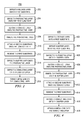
- FIG. 2 illustrates an example method for producing the thin-film photovoltaic cell device stack of FIG. 1C .
- FIGS. 3A-3D illustrate various stages of an example thin-film photovoltaic cell device stack with a reverse stack structure produced using a removable substrate and a buffer layer comprising a metal.
- FIG. 4 illustrates an example method for producing the thin-film photovoltaic cell device stack of FIG. 3D .
- FIGS. 5A-5B illustrate various stages of an example thin-film photovoltaic cell device stack with a reverse stack structure produced using a buffer layer comprising a metal.
- FIG. 6 illustrates an example method for producing the thin-film photovoltaic cell device stack of FIG. 5B .
- FIGS. 7A-7C illustrate example configurations of a portion of a thin-film photovoltaic cell for enhancing the current carrying capacity of the thin-film photovoltaic cell.
- Typical device stacks for thin-film photovoltaic cells include various layers that interact to produce electric current from a light source.
- production of a typical device stack may include forming a contact layer on a substrate, such as glass or foil.
- a photoactive layer is then formed on the contact layer.
- a buffer layer such as cadmium sulfide (CdS)
- CBD chemical bath deposition
- sputtering is then formed on the buffer layer and a metal grid is formed on the conducting layer.
- TCO transparent conducting oxide
- the various layers of the device stack are built in a reverse order.
- the process begins by forming a conducting layer (typically TCO) on a transparent substrate.
- the buffer layer is formed on the conducting layer and the photoactive layer is formed on the buffer layer.
- a contact layer is then formed on the photoactive layer to complete the stack.
- a removable substrate may be used as a foundation to build the photoactive layer and contact layer and may be removed once an additional substrate is attached to the contact layer. The removable substrate may then be reused during the production of additional device stacks.
- the additional substrate is flexible, enhancing the versatility of the resulting device stack.
- a buffer layer comprising a metal is deposited to the device stack and the metal is allowed to interact with a chalcogen of the photoactive layer to form a semiconducting material within the buffer layer.
- CdS which is hazardous and toxic
- Other embodiments may include the formation of wires within a substrate or the conducting layer to improve current flow within the device stack.
- FIGS. 1A-1C illustrate various stages of an example thin-film photovoltaic cell device stack 140 with a reverse stack structure produced using a removable substrate 104 .
- FIGS. 1A-1C will be described in conjunction with FIG. 2 which illustrates an example method 200 for producing the thin-film photovoltaic cell device stack 140 c of FIG. 1C .
- Method 200 begins at step 202 as a release layer is deposited onto a first substrate.
- the first substrate may be removable substrate 104 and the release layer may be release layer 108 .
- Substrate 104 may be any suitable substrate capable of withstanding high temperatures and/or pressures.
- Substrate 104 may provide structural support for the film stack 140 .
- substrate 104 may be soda-lime glass, a metal sheet or foil (e.g., stainless steel, aluminum, tungsten), a semiconductor (e.g., Si, Ge, GaAs), a polymer, another suitable substrate, or any combination thereof.
- soda-lime glass is used and provides sodium to the photoactive layer 112 during annealing to promote grain growth.
- a different substrate material is used and a material containing sodium, such as NaFl is deposited close to photoactive layer 112 to promote grain growth during annealing.
- Release layer 108 may facilitate the removal of substrate 104 from the remainder of the stack 140 at a later point in the manufacturing process.
- release layer 108 is very thin.
- release layer 108 may comprise a thin layer of Boron Nitride (BN).
- Release layer 108 may include a material that does not impede the flow of sodium from the substrate 104 to the photoactive layer 112 during annealing or other subsequent processing of the stack 140 .
- a photoactive layer is deposited onto the first substrate.
- photoactive layer 112 is deposited onto substrate 104 .
- photoactive layer 112 may be deposited directly onto substrate 104 or onto one or more other layers (such as release layer 108 ) that are deposited onto substrate 104 .
- Photoactive layer 112 may be either a p-type or an n-type semiconductor layer.
- Photoactive layer 112 may be any suitable material, such as a copper indium gallium sulfur/selenide (CIGS), copper zinc tin sulfur/selenide (CZTS), (CIGS), or CdTe thin-film as described herein.
- CGS copper indium gallium sulfur/selenide
- CZTS copper zinc tin sulfur/selenide
- CdTe thin-film as described herein.
- CIGS materials include copper indium gallium diselenide (e.g., Cu(In 1-x Ga x )Se 2 , where x is less than or equal to approximately 0.7), copper indium gallium selenide sulfide (e.g., Cu(In 1-x Ga x )(Se 1-y S y ) 2 , where x is less than or equal to approximately 0.7 and y is less than or equal to approximately 0.99), and copper indium gallium disulfide (e.g., Cu(In 1-x Ga x )S 2 , where x is less than or equal to approximately 0.7).
- copper indium gallium diselenide e.g., Cu(In 1-x Ga x )Se 2 , where x is less than or equal to approximately 0.7
- copper indium gallium selenide sulfide e.g., Cu(In 1-x Ga x )(Se 1-y S y ) 2 , where x is less than or equal
- CIGS have been successfully used in the fabrication of thin film absorbers (i.e., photoactive layers) in photovoltaic cells largely due to their relatively large absorption coefficients.
- photovoltaic cells having photovoltaic efficiencies greater than or equal to approximately 20% have been manufactured using copper indium gallium diselenide absorber layers.
- Efforts to minimize the defect density in the absorber layer(s) have enabled the manufacture of high quality CIGS thin film photovoltaic cells.
- reducing the defect density in the absorber layer may be achieved by heating the CIGS material close to its melting temperature, which facilitates grain growth and defect removal in the absorber layer.
- CZTS materials have a favorable direct band gap (1.45 eV), a large absorption coefficient (>10 4 cm ⁇ 1 ), and are formed entirely from non-toxic, abundant elements that are produced in large quantities.
- CZTS also shares a number of similarities with CIGS as the equipment and processes used for deposition of these two materials are very similar.
- CZTS materials can be synthesized through solid-state chemical reactions between Zn(S, Se), Cu 2 (S, Se), and Sn(S, Se) 2 .
- the CZTS material may comprise Cu 2 ZnSn(S, Se) 4 .
- Various compositions of CZTS materials are described in U.S. application Ser. No. 13/401,512, the text of which is incorporated by reference herein.
- the deposition of photoactive layer 112 may include applying a combination of the constituent elements (e.g., copper, indium, gallium, sulfur, and selenium for CIGS and copper, zinc, tin, sulfur, and selenium for CZTS) to substrate 104 .
- a combination of the constituent elements e.g., copper, indium, gallium, sulfur, and selenium for CIGS and copper, zinc, tin, sulfur, and selenium for CZTS
- Any suitable combination of the constituent elements may be used.
- this disclosure illustrates particular constituent materials used to form photoactive layer 112 , this disclosure contemplates any suitable constituent materials with any suitable compositions or architectures.
- additional constituents such as alkali metal salts, antimony, bismuth, another suitable constituent, or any combination thereof may be added to photoactive layer 112 to enhance its properties (e.g., grain size) or performance.
- photoactive layer 112 may contain up to approximately 20 atomic % of one or more of Al, Si, Ti, V, Zn, Ga, Zr, Nb, Mo, Ru, Pd, In, Sn, Ta, W, Re, Ir, Pt, Au, Pb, or Bi.
- Deposition of the constituent materials may be performed using any suitable thin-film deposition process, such as, for example, chemical-vapor deposition, evaporation, atomic-layer deposition, sputtering, particle coating, spray pyrolysis, spin-coating, electro-deposition, electrochemical deposition, photoelectrochemical deposition, hot-injection, chemical-bath deposition, spin coating, another suitable deposition process, or any combination thereof.
- suitable thin-film deposition process such as, for example, chemical-vapor deposition, evaporation, atomic-layer deposition, sputtering, particle coating, spray pyrolysis, spin-coating, electro-deposition, electrochemical deposition, photoelectrochemical deposition, hot-injection, chemical-bath deposition, spin coating, another suitable deposition process, or any combination thereof.
- a contact layer is deposited onto the photoactive layer.
- contact layer 116 is deposited onto photoactive layer 112 .
- Contact layer 116 may be any suitable electrode material, such as, for example, Mo, W, Al, Fe, Cu, Sn, Zn, another suitable electrode material, or any combination thereof.
- Contact layer 116 may be deposited onto photoactive layer 112 in any suitable manner, such as sputtering.
- Contact layer 116 may be deposited onto photoactive layer 112 at any suitable time during manufacturing of the stack 140 , such as before annealing or after annealing.
- contact layer 116 includes a metal such as Mo and the contact layer is applied before annealing.
- an excess material from photoactive layer may combine with the metal to form a layer between the contact layer 116 and the photoactive layer 112 that results in an enhanced electrical response of the stack 140 .
- this layer may comprise Molybdenum Selenide (MoSe 2 ).
- contact layer 116 is transparent to allow light penetration into photoactive layer 112 .
- the photoactive layer is annealed.
- photoactive layer 112 may be annealed at a high temperature (e.g., approximately >500° C.) to form a crystalline phase in the photoactive layer 112 .
- a high temperature e.g., approximately >500° C.
- Any suitable type of annealing may be used, such as pulsed annealing, flash annealing, laser annealing, furnace annealing, lamp annealing, another suitable annealing process, or any combination thereof.
- Annealing may be performed using any suitable source such as a light source (e.g., a halogen lamp or a laser), resistive heaters, lasers, another suitable heating source, or any combination thereof.
- the annealing may utilize any suitable process of heating, such as conduction, convection, radiation, or any combination thereof.
- the heating may be effected either directly onto the surface of a film layer or via a back substrate.
- the annealing is performed by a belt furnace using a combination of conduction, convection, and radiation.
- sodium from a lime-glass substrate 104 or other suitable sodium source may promote grain growth in photoactive layer 112 .
- a second substrate is attached onto the contact layer.
- substrate 124 is attached to contact layer 116 .
- Substrate 124 may be any suitable material, such as soda-lime glass, a metal sheet or foil (e.g., stainless steel, aluminum, tungsten), a semiconductor (e.g., Si, Ge, GaAs), a polymer, another suitable substrate, or any combination thereof.
- the second substrate 124 is a flexible metallic foil.
- Substrate 124 may be attached to contact layer 116 in any suitable manner, such as via conductive adhesive 120 .
- Conductive adhesive 120 may be any suitable material for adhering contact layer 116 to substrate 124 .
- conductive adhesive 120 comprises silver epoxy. Conductive adhesive 120 may be cured by drying and/or heating.
- the first substrate is removed.
- substrate 104 may be separated from the remainder of the stack 140 b .
- the remainder of the stack 140 b is lifted-off and/or peeled from substrate 104 (and release layer 108 if present).
- Substrate 104 may then be cleaned and/or re-conditioned and reused in production of another stack.
- the remainder of the stack 140 b may undergo subsequent processing, such as that shown in FIG. 1C .
- a buffer layer is deposited onto the photoactive layer.
- buffer layer 128 is deposited on photoactive layer 112 .
- buffer layer 128 may form a p-n junction with photoactive layer 112 .
- Buffer layer 128 may be either a p-type or an n-type semiconductor layer.
- buffer layer 128 may include one or more of the following semiconductor materials: silicon (Si), germanium (Ge), tin (Sn), beta iron silicide ( ⁇ -FeSi 2 ), indium antimony (InSb), indium arsenic (InAs), indium phosphate (InP), gallium phosphate (GaP), aluminum phosphate (AlP), gallium arsenic (GaAs), gallium antimony (GaSb), aluminum antimony (AlSb), silicon carbide (SiC), tellurium (Te), zinc antimony (ZnSb), mercury telluride (HgTe), led sulfide (PbS), led selenide (PbSe), led telluride (PbTe), cadmium sulfide (CdS), cadmium selenide (CdSe), cadmium telluride (CdTe), zinc sulfide (ZnS), zinc selenide (ZnS), zinc
- one or more of photoactive layer 112 or buffer layer 128 may also contain up to 80 vol. % of an oxide material selected from the group consisting of magnesium (Mg) oxide, aluminum (Al) oxide, silicon (Si) oxide, titanium (Ti) oxide, vanadium (V) oxide, chromium (Cr) oxide, manganese (Mn) oxide, iron (Fe) oxide, cobalt (Co) oxide, nickel (Ni) oxide, copper (Cu) oxide, zinc (Zn) oxide, gallium (Ga) oxide, germanium (Ge) oxide, selenium (Se) oxide, yttrium (Y) oxide, zirconium (Zr) oxide, niobium (Nb) oxide, molybdenum (Mo) oxide, indium (In) oxide, tin (Sn) oxide, antimony (Sb) oxide, tellurium (Tl) oxide, hafnium (Hf) oxide, tantalum (Ta) oxide, tungsten (W)
- buffer layer 128 may include one or more of the following n-type semiconductor materials: silicon (Si), germanium (Ge), tin (Sn), beta iron silicide ( ⁇ -FeSi 2 ), indium antimony (InSb), indium arsenic (InAs), indium phosphate (InP), gallium phosphate (GaP), aluminum phosphate (AlP), gallium arsenic (GaAs), gallium antimony (GaSb), aluminum antimony (AlSb), silicon carbide (SiC), tellurium (Te), zinc antimony (ZnSb), mercury telluride (HgTe), led sulfide (PbS), led selenide (PbSe), led telluride (PbTe), cadmium sulfide (CdS), cadmium selenide (CdSe), cadmium telluride (CdTe), zinc sulfide (ZnS), zinc selenide (Zn
- buffer layer 128 may include one or more of the following p-type semiconductor materials: silicon (Si), germanium (Ge), tin (Sn), beta iron silicide ( ⁇ -FeSi 2 ), indium antimony (InSb), indium arsenic (InAs), indium phosphate (InP), gallium phosphate (GaP), aluminum phosphate (AlP), gallium arsenic (GaAs), gallium antimony (GaSb), aluminum antimony (AlSb), silicon carbide (SiC), tellurium (Te), zinc antimony (ZnSb), mercury telluride (HgTe), led sulfide (PbS), led selenide (PbSe), led telluride (PbTe), cadmium sulfide (CdS), cadmium selenide (CdSe), cadmium telluride (CdTe), zinc sulfide (ZnS), zinc selenide (Zn
- Such semiconductors may be doped by adding an impurity of valence-three elements such as boron (B), gallium (Ga), indium (In), or aluminum (Al), in order to increase the number of free (in this case positive (hole)) charge carriers.
- buffer layer 128 may also contain up to 80 vol.
- conducting layer 132 is deposited onto buffer layer 128 .
- conducting layer 132 may be a transparent conducting oxide (TCO), such as, for example, ZnO/Al, In 2 O 3 /Sn, another suitable transparent conducting oxide, or any combination thereof.
- TCO transparent conducting oxide
- a metal grid is formed on the conducting layer.
- metal grid 136 is formed on conducting layer 132 .
- metal grid 136 is deposited using screen-printing.
- Metal grid 136 may be arranged in a grid (e.g., fingers and busbars) on one side (or both sides) and a full area metal contact on the other side.
- Conducting layer 132 and metal grid 136 may facilitate the flow of current in the stack 140 . Additional layers, such as anti-reflection coatings may also be added to the stack.
- a sodium containing substrate 104 such as soda-lime glass may be used to promote positive grain growth in photoactive layer 112 and then removed from the stack. This may result in a photoactive layer 112 with reduced surface roughness that forms an improved p/n junction with buffer layer 128 . Because the substrate 104 is removable, any suboptimal optical characteristics of the soda-lime glass or other material do not affect the operation of stack 140 . Moreover, the substrate 104 may be reused to produce additional device stacks. As another example, in particular embodiments, a flexible substrate 124 may be added to device stack 140 resulting in increased versatility of the stack.
- FIGS. 1A-1C illustrate particular arrangements of substrate 124 , contact layer 116 , photoactive layer 112 , buffer layer 128 , conducting layer 132 , metal grid 136 , release layer 108 , and substrate 104 this disclosure contemplates any suitable arrangement of substrate 124 , contact layer 116 , photoactive layer 112 , buffer layer 128 , conducting layer 132 , metal grid 136 , release layer 108 , and substrate 104 .
- FIGS. 1A-1C illustrate particular arrangements of substrate 124 , contact layer 116 , photoactive layer 112 , buffer layer 128 , conducting layer 132 , metal grid 136 , release layer 108 , and substrate 104 .
- FIGS. 1A-1C illustrate particular arrangements of substrate 124 , contact layer 116 , photoactive layer 112 , buffer layer 128 , conducting layer 132 , metal grid 136 , release layer 108 , and substrate 104 this disclosure contemplates any suitable arrangement of substrate 124 , contact layer 116 ,
- FIG. 1A-1C illustrate a particular number of substrates 124 , contact layers 116 , photoactive layers 112 , buffer layers 128 , conducting layers 132 , metal grids 136 , release layers 108 , and substrates 104
- this disclosure contemplates any suitable number of substrates 124 , contact layers 116 , photoactive layers 112 , buffer layers 128 , conducting layers 132 , metal grids 136 , release layers 108 , and substrates 104 .
- device stack 140 may include multiple photoactive layers 112 and buffer layers 128 , forming multiple p-n junctions.
- one or more layers of device stack 140 may be deposited using any suitable method such as one or more of chemical-vapor deposition, evaporation, atomic-layer deposition, sputtering, particle coating, spray pyrolysis, spin-coating, electro-deposition, electrochemical deposition, photoelectrochemical deposition, hot-injection, another suitable deposition process, or any combination thereof.
- Particular embodiments may repeat one or more steps of the method of FIG. 2 , where appropriate.
- this disclosure describes and illustrates particular steps of the method of FIG. 2 as occurring in a particular order, this disclosure contemplates any suitable steps of the method of FIG. 2 occurring in any suitable order.
- one or more steps may be omitted.
- the deposition of a release layer may be omitted and the photoactive layer may be deposited directly on the substrate at step 204 .
- this disclosure describes and illustrates particular components, devices, or systems carrying out particular steps of the method of FIG. 2
- this disclosure contemplates any suitable combination of any suitable components, devices, or systems carrying out any suitable steps of the method of FIG. 2 .
- FIGS. 3A-3D illustrate various stages of an example thin-film photovoltaic cell device stack 340 with a reverse stack structure produced using a removable substrate 304 and a buffer layer 310 a comprising a metal.
- FIGS. 3A-3D will be described in conjunction with FIG. 4 which illustrates an example method 400 for producing the thin-film photovoltaic cell device stack 340 of FIG. 3D .
- Method 400 begins at step 402 as a release layer is deposited onto a first substrate.
- the first substrate may be removable substrate 304 and the release layer may be release layer 308 .
- Substrate 304 and release layer 308 may have any of the characteristics described above in connection with substrate 104 and release layer 108 .
- buffer layer 310 a is deposited onto substrate 304 .
- buffer layer 310 a may be deposited directly onto substrate 304 or onto one or more other layers (such as release layer 308 ) that are deposited onto substrate 304 .
- Buffer layer 310 a may have any of the characteristics described above in connection with buffer layer 128 .
- buffer layer 310 a substantially or completely comprises a metal that is operable to interact with one or more chalcogens of photoactive layer 312 to form a semiconductor material, such as an n-type semiconductor.
- the metal of buffer layer 310 a is Mo and a chalcogen that the metal interacts with is Se or S.
- the Mo interacts with excess Se from the photoactive layer 312 to form MoSe 2 .
- buffer layers 310 b in FIGS. 3B-3D are provided as examples only and not by way of limitation. That is, the metal of buffer layer 310 a and the one or more chalcogens of the photoactive layer 312 may form any suitable semiconductor material.
- the thickness of buffer layer 310 a is within the range of approximately 10 to 50 nanometers (nm).
- a photoactive layer is deposited onto the buffer layer.
- photoactive layer 312 is deposited onto buffer layer 310 a .
- Photoactive layer 312 may include any of the characteristics described above in connection with photoactive layer 112 .
- photoactive layer 312 may include an excess of one or more chalcogens capable of bonding with a metal of buffer layer 310 a to form a semiconductor material.
- a contact layer is deposited onto the photoactive layer.
- contact layer 316 is deposited onto photoactive layer 312 .
- Contact layer 316 may have any of the characteristics described above in connection with contact layer 116 .
- the photoactive layer and the buffer layer are annealed.
- photoactive layer 312 and buffer layer 310 a may be annealed at a high temperature (e.g., approximately >500° C.) to form a crystalline phase in the photoactive layer 312 and to form a semiconductor material from the metal of buffer layer 310 a and the one or more excess chalcogens of photoactive layer 312 .
- the bonding of the metal of buffer layer 310 a and the one or more excess chalcogens of photoactive layer 312 is depicted by way of example in FIG. 3B where buffer layer 310 b is shown as comprising MoSe 2 .
- the photoactive layer 312 and buffer layer 310 a may be annealed in any suitable manner such as a manner described above in connection with step 208 .
- a second substrate is attached to the contact layer.
- substrate 324 is attached to contact layer 316 .
- Substrate 324 may have any of the characteristics described above in connection with substrate 124 and may be attached to contact layer 316 in any suitable manner, such as by conductive adhesive 320 which may have any of the characteristics described above in connection with conductive adhesive 120 .
- the first substrate is removed.
- substrate 304 may be separated from the remainder of the stack 340 c .
- the remainder of the stack 340 c is lifted-off and/or peeled from substrate 304 (and release layer 308 if present).
- Substrate 304 may then be cleaned and/or re-conditioned and reused in production of another stack.
- the remainder of the stack 340 c may undergo subsequent processing, such as that shown in FIG. 3D .
- a conducting layer is deposited onto the buffer layer.
- conducting layer 332 is deposited onto buffer layer 310 b .
- Conducting layer 332 may have any of the characteristics described above in connection with conducting layer 132 .
- a metal grid is formed on the conducting layer.
- metal grid 336 is formed on conducting layer 332 .
- Metal grid 336 may have any of the characteristics described above in connection with metal grid 136 . Additional layers, such as anti-reflection coatings may also be added to the stack 340 d.
- a low-cost soda-lime glass may be used as substrate 304 to promote positive grain growth in photoactive layer 312 and then removed from the stack 340 . Accordingly, any suboptimal optical characteristics of the soda-lime glass do not affect the operation of stack 340 .
- a flexible substrate 324 may be added to increase the versatility of stack 340 .
- the difficult and expensive application of a hazardous material such as CdS as a buffer layer may be avoided by instead applying a metal to the first substrate 304 and allowing the metal to interact with one or more chalcogens of the photoactive layer to form a semiconductor material within buffer layer 310 b.
- FIGS. 3A-3D illustrate particular arrangements of substrate 324 , contact layer 316 , photoactive layer 312 , buffer layer 310 , conducting layer 332 , metal grid 336 , release layer 308 , and substrate 304 this disclosure contemplates any suitable arrangement of substrate 324 , contact layer 316 , photoactive layer 312 , buffer layer 310 , conducting layer 332 , metal grid 336 , release layer 308 , and substrate 304 .
- FIGS. 3A-3D illustrate particular arrangements of substrate 324 , contact layer 316 , photoactive layer 312 , buffer layer 310 , conducting layer 332 , metal grid 336 , release layer 308 , and substrate 304 .
- FIGS. 3A-3D illustrate particular arrangements of substrate 324 , contact layer 316 , photoactive layer 312 , buffer layer 310 , conducting layer 332 , metal grid 336 , release layer 308 , and substrate 304 this disclosure contemplates any suitable arrangement of substrate 324 , contact layer 316 ,
- 3A-3D illustrate a particular number of substrates 324 , contact layers 316 , photoactive layers 312 , buffer layers 310 , conducting layers 332 , metal grids 336 , release layers 308 , and substrates 304 this disclosure contemplates any suitable number of substrates 324 , contact layers 316 , photoactive layers 312 , buffer layers 310 , conducting layers 332 , metal grids 336 , release layers 308 , and substrates 304 .
- device stack 340 may include multiple photoactive layers 112 and buffer layers 128 , forming multiple p-n junctions.
- U.S. application Ser. No. 12/953,867, U.S. application Ser. No. 12/016,172, U.S. application Ser. No. 11/923,036, and U.S. application Ser. No. 11/923,070 disclose additional layer arrangements and configurations for photovoltaic cell structures that may be used with particular embodiments disclosed herein.
- one or more layers of device stack 340 may be deposited using any suitable method such as one or more of chemical-vapor deposition, evaporation, atomic-layer deposition, sputtering, particle coating, spray pyrolysis, spin-coating, electro-deposition, electrochemical deposition, photoelectrochemical deposition, hot-injection, another suitable deposition process, or any combination thereof.
- Particular embodiments may repeat one or more steps of the method of FIG. 4 , where appropriate.
- this disclosure describes and illustrates particular steps of the method of FIG. 4 as occurring in a particular order, this disclosure contemplates any suitable steps of the method of FIG. 4 occurring in any suitable order.
- one or more steps may be omitted.
- the deposition of a release layer may be omitted and the buffer layer may be deposited directly on the substrate at step 404 .
- this disclosure describes and illustrates particular components, devices, or systems carrying out particular steps of the method of FIG. 4
- this disclosure contemplates any suitable combination of any suitable components, devices, or systems carrying out any suitable steps of the method of FIG. 4 .
- FIGS. 5A-5B illustrate various stages of an example thin-film photovoltaic cell device stack 540 with a reverse stack structure produced using a buffer layer 510 a comprising a metal.
- FIGS. 5A-5B will be described in conjunction with FIG. 6 which illustrates an example method 600 for producing the thin-film photovoltaic cell device stack 540 b of FIG. 5B .
- Method 600 begins at step 602 , where wires are formed within a conducting layer or substrate. These wires will be described in more detail in connection with FIGS. 7A-7C . This step may occur at any suitable time, such as before step 604 , concurrently with step 604 , or after step 604 .
- the conducting layer is deposited on the substrate.
- conducting layer 532 is deposited on substrate 504 .
- Substrate 504 may have any of the characteristics described above in connection with substrate 104 .
- substrate 504 may be subjected to high temperatures without substantial detrimental effects to substrate 504 .
- Conducting layer 532 may have any of the characteristics described above in connection with conducting layer 132 .
- conducting layer 532 is a TCO, such as fluorinated tin oxide (FTO) or Indium Tin Oxide (ITO), that is coated on substrate 504 .
- the thickness of conducting layer 532 is selected to minimize absorption.
- the materials and characteristics of substrate 504 and conducting layer 532 may be chosen so that the combination of substrate 504 and conducting layer 532 has low reflectance, low absorbance, and high transmittance over a relevant spectral range.
- buffer layer 510 a is deposited onto conducting layer 532 .
- Buffer layer 510 a may have any of the characteristics described above in connection with buffer layers 310 a or 128 .
- buffer layer 510 a substantially or completely comprises a metal that is operable to interact with one or more chalcogens of photoactive layer 312 to form a semiconductor material, such as an n-type semiconductor.
- the metal of buffer layer 510 a is Mo and a chalcogen that the metal interacts with is Se or S.
- the Mo interacts with excess Se from the photoactive layer 512 to form MoSe 2 .
- buffer layer 510 b Such embodiments are depicted by buffer layer 510 b in FIG. 5B which is provided as an example only and not by way of limitation.
- the metal of buffer layer 510 a and the one or more chalcogens of the photoactive layer 512 may form any suitable semiconductor material.
- the thickness of buffer layer 510 a is within the range of approximately 10 to 50 nanometers (nm).
- a photoactive layer is deposited onto the buffer layer.
- photoactive layer 512 is deposited onto buffer layer 510 a .
- Photoactive layer 512 may include any of the characteristics described above in connection with photoactive layers 312 and 112 . As described above, in particular embodiments, photoactive layer 512 may include an excess of one or more chalcogens capable of bonding with a metal of buffer layer 510 a to form a semiconductor material.
- a contact layer is deposited onto the photoactive layer.
- contact layer 516 is deposited onto photoactive layer 512 .
- Contact layer 516 may have any of the characteristics described above in connection with contact layer 116 .
- the photoactive layer and the buffer layer are annealed.
- photoactive layer 512 and buffer layer 510 a may be annealed at a high temperature (e.g., approximately >500° C.) to form a crystalline phase in the photoactive layer 512 and to form a semiconductor material from the metal of buffer layer 510 a and the one or more excess chalcogens of photoactive layer 512 .
- the bonding of the metal of buffer layer 510 a and the one or more excess chalcogens of photoactive layer 512 is depicted by way of example in FIG. 5B where buffer layer 510 b is shown as comprising MoSe 2 .
- the photoactive layer 512 and buffer layer 510 a may be annealed in any suitable manner such as a manner described above in connection with step 208 .
- One or more of the various embodiments described above in connection with FIGS. 5A-5B and FIG. 6 may provide advantages over previous methods of thin film cell production.
- the difficult and expensive application of a hazardous material such as CdS as a buffer layer may be avoided by instead applying a metal to the conducting layer and allowing the metal to interact with one or more chalcogens of the photoactive layer 512 to form a semiconductor material within a buffer layer 510 .
- FIGS. 5A-5B illustrate particular arrangements of substrate 504 , conducting layer 532 , buffer layer 510 , photoactive layer 512 , and contact layer 516
- this disclosure contemplates any suitable arrangement of substrate 504 , conducting layer 532 , buffer layer 510 , photoactive layer 512 , and contact layer 516 .
- FIGS. 5A-5B illustrate a particular number of substrates 504 , conducting layers 532 , buffer layers 510 , photoactive layers 512 , and contact layers 516 this disclosure contemplates any suitable number of substrates 504 , conducting layers 532 , buffer layers 510 , photoactive layers 512 , and contact layers 516 .
- device stack 540 may include multiple photoactive layers 512 and buffer layers 510 , forming multiple p-n junctions.
- U.S. application Ser. No. 12/953,867, U.S. application Ser. No. 12/016,172, U.S. application Ser. No. 11/923,036, and U.S. application Ser. No. 11/923,070 disclose additional layer arrangements and configurations for photovoltaic cell structures that may be used with particular embodiments disclosed herein.
- one or more layers of device stack 540 may be deposited using any suitable method such as one or more of chemical-vapor deposition, evaporation, atomic-layer deposition, sputtering, particle coating, spray pyrolysis, spin-coating, electro-deposition, electrochemical deposition, photoelectrochemical deposition, hot-injection, another suitable deposition process, or any combination thereof.
- Particular embodiments may repeat one or more steps of the method of FIG. 6 , where appropriate.
- this disclosure describes and illustrates particular steps of the method of FIG. 6 as occurring in a particular order, this disclosure contemplates any suitable steps of the method of FIG. 6 occurring in any suitable order. In particular embodiments, one or more steps may be omitted.
- this disclosure describes and illustrates particular components, devices, or systems carrying out particular steps of the method of FIG. 6 , this disclosure contemplates any suitable combination of any suitable components, devices, or systems carrying out any suitable steps of the method of FIG. 6 .
- FIGS. 7A-7C illustrate example configurations of a portion of a thin-film photovoltaic cell for enhancing the current carrying capacity of the thin-film photovoltaic cell.
- the portion of the photovoltaic cell shown in FIGS. 7A-7C corresponds to the conducting layer 532 and substrate 504 of FIGS. 5A-5B .
- the structure and methods shown may apply to any suitable substrate and conducting layer.
- FIGS. 7A-7C illustrate the addition of wires to the conducting layer 532 or substrate 504 to improve the current carrying capacity of the conducting layer 532 .
- the wires may be formed in any suitable pattern, such as a mesh or grid in conducting layer 532 or substrate 504 .
- FIGS. 7A-7C depict a single wire, though particular embodiments include any suitable number of wires.
- an example wire 702 is disposed in a recessed portion 704 (e.g., a groove) of substrate 504 .
- the recessed portions 704 into which wires 702 are placed are formed on substrate 504 prior to the deposition of the conducting layer 532 onto substrate 504 .
- the wires 702 are placed such that they maintain electrical contact with conducting layer 532 .
- wire 702 is disposed within conducting layer 532 .
- wires 702 are placed within conducting layer 532 during the deposition of conducting layer 532 onto substrate 504 .
- wire 702 is disposed in a recessed portion (e.g., a groove) of conducting layer 532 .
- the recessed portions 706 into which wires 702 are placed are formed on conducting layer 532 after conducting layer 532 has been deposited onto substrate 504 .
- the wires 702 are placed such that they maintain electrical contact with conducting layer 532 .
- an apparatus or system or a component of an apparatus or system being adapted to, arranged to, capable of, configured to, enabled to, operable to, or operative to perform a particular function encompasses that apparatus, system, component, whether or not it or that particular function is activated, turned on, or unlocked, as long as that apparatus, system, or component is so adapted, arranged, capable, configured, enabled, operable, or operative.
Landscapes
- Photovoltaic Devices (AREA)
- Life Sciences & Earth Sciences (AREA)
- Engineering & Computer Science (AREA)
- Sustainable Development (AREA)
- Sustainable Energy (AREA)
Abstract
Description
Claims (19)
Priority Applications (2)
| Application Number | Priority Date | Filing Date | Title |
|---|---|---|---|
| US13/452,603 US8993370B2 (en) | 2012-04-20 | 2012-04-20 | Reverse stack structures for thin-film photovoltaic cells |
| US14/672,708 US20150340515A1 (en) | 2012-04-20 | 2015-03-30 | Reverse stack structures for thin-film photovoltaic cells |
Applications Claiming Priority (1)
| Application Number | Priority Date | Filing Date | Title |
|---|---|---|---|
| US13/452,603 US8993370B2 (en) | 2012-04-20 | 2012-04-20 | Reverse stack structures for thin-film photovoltaic cells |
Related Child Applications (1)
| Application Number | Title | Priority Date | Filing Date |
|---|---|---|---|
| US14/672,708 Division US20150340515A1 (en) | 2012-04-20 | 2015-03-30 | Reverse stack structures for thin-film photovoltaic cells |
Publications (2)
| Publication Number | Publication Date |
|---|---|
| US20130276888A1 US20130276888A1 (en) | 2013-10-24 |
| US8993370B2 true US8993370B2 (en) | 2015-03-31 |
Family
ID=49378994
Family Applications (2)
| Application Number | Title | Priority Date | Filing Date |
|---|---|---|---|
| US13/452,603 Expired - Fee Related US8993370B2 (en) | 2012-04-20 | 2012-04-20 | Reverse stack structures for thin-film photovoltaic cells |
| US14/672,708 Abandoned US20150340515A1 (en) | 2012-04-20 | 2015-03-30 | Reverse stack structures for thin-film photovoltaic cells |
Family Applications After (1)
| Application Number | Title | Priority Date | Filing Date |
|---|---|---|---|
| US14/672,708 Abandoned US20150340515A1 (en) | 2012-04-20 | 2015-03-30 | Reverse stack structures for thin-film photovoltaic cells |
Country Status (1)
| Country | Link |
|---|---|
| US (2) | US8993370B2 (en) |
Cited By (1)
| Publication number | Priority date | Publication date | Assignee | Title |
|---|---|---|---|---|
| US20140353700A1 (en) * | 2013-05-30 | 2014-12-04 | International Business Machines Corporation | Heterojunction light emitting diode |
Families Citing this family (8)
| Publication number | Priority date | Publication date | Assignee | Title |
|---|---|---|---|---|
| US9685569B2 (en) * | 2014-03-11 | 2017-06-20 | Taiwan Semiconductor Manufacturing Co., Ltd. | Method of CIGS absorber formation |
| US10453978B2 (en) * | 2015-03-12 | 2019-10-22 | International Business Machines Corporation | Single crystalline CZTSSe photovoltaic device |
| US20160268460A1 (en) * | 2015-03-12 | 2016-09-15 | International Business Machines Corporation | SINGLE CRYSTALLINE CZTSSe PHOTOVOLTAIC DEVICE |
| US9935214B2 (en) | 2015-10-12 | 2018-04-03 | International Business Machines Corporation | Liftoff process for exfoliation of thin film photovoltaic devices and back contact formation |
| WO2018064143A1 (en) * | 2016-09-27 | 2018-04-05 | Board Of Regents, The University Of Texas System | Bacterial cellulose paper-based flexible electronics employing nanocrystals |
| US10014423B2 (en) * | 2016-09-30 | 2018-07-03 | International Business Machines Corporation | Chalcogen back surface field layer |
| US10553743B2 (en) | 2017-11-20 | 2020-02-04 | The Government Of The United States Of America, As Represented By The Secretary Of The Navy | Flexible crystalline ultra-thin Si solar cells |
| US12119367B2 (en) * | 2020-07-24 | 2024-10-15 | University Of Southern California | Composite substrate for fabricating III-V photodetector arrays |
Citations (3)
| Publication number | Priority date | Publication date | Assignee | Title |
|---|---|---|---|---|
| US20050186805A1 (en) * | 2001-09-20 | 2005-08-25 | Stanbery Billy J. | Synthesis of layers, coatings or films using collection layer |
| US20080075927A1 (en) * | 2005-06-07 | 2008-03-27 | Fujiflim Corporation | Functional Film Containing Structure And Method Of Manufacturing Functional Film |
| US20130269778A1 (en) * | 2012-04-13 | 2013-10-17 | Tsmc Solar Ltd. | Cigs solar cell structure and method for fabricating the same |
-
2012
- 2012-04-20 US US13/452,603 patent/US8993370B2/en not_active Expired - Fee Related
-
2015
- 2015-03-30 US US14/672,708 patent/US20150340515A1/en not_active Abandoned
Patent Citations (3)
| Publication number | Priority date | Publication date | Assignee | Title |
|---|---|---|---|---|
| US20050186805A1 (en) * | 2001-09-20 | 2005-08-25 | Stanbery Billy J. | Synthesis of layers, coatings or films using collection layer |
| US20080075927A1 (en) * | 2005-06-07 | 2008-03-27 | Fujiflim Corporation | Functional Film Containing Structure And Method Of Manufacturing Functional Film |
| US20130269778A1 (en) * | 2012-04-13 | 2013-10-17 | Tsmc Solar Ltd. | Cigs solar cell structure and method for fabricating the same |
Cited By (3)
| Publication number | Priority date | Publication date | Assignee | Title |
|---|---|---|---|---|
| US20140353700A1 (en) * | 2013-05-30 | 2014-12-04 | International Business Machines Corporation | Heterojunction light emitting diode |
| US9252324B2 (en) * | 2013-05-30 | 2016-02-02 | Globalfoundries Inc | Heterojunction light emitting diode |
| US9343616B2 (en) | 2013-05-30 | 2016-05-17 | Globalfoundries Inc. | Heterojunction light emitting diode |
Also Published As
| Publication number | Publication date |
|---|---|
| US20130276888A1 (en) | 2013-10-24 |
| US20150340515A1 (en) | 2015-11-26 |
Similar Documents
| Publication | Publication Date | Title |
|---|---|---|
| US20150340515A1 (en) | Reverse stack structures for thin-film photovoltaic cells | |
| TWI478367B (en) | Solar cell and method of manufacturing same | |
| US20110174363A1 (en) | Control of Composition Profiles in Annealed CIGS Absorbers | |
| KR101893411B1 (en) | A preparation method of solar cell using ZnS buffer layer | |
| JP5928612B2 (en) | Compound semiconductor solar cell | |
| KR20140099865A (en) | Conductive substrate for a photovoltaic cell | |
| KR101908475B1 (en) | A solar cell comprising CZTS Thin film with a oxide buffer layer and a method of manufacturing the same | |
| JP2011205098A (en) | Thin film photovoltaic cell | |
| US9748419B2 (en) | Back contact design for solar cell, and method of fabricating same | |
| CN106653946A (en) | Method for depositing cadmium telluride film solar cell absorption layer | |
| US20130029450A1 (en) | Method for manufacturing solar cell | |
| US8822816B2 (en) | Niobium thin film stress relieving layer for thin-film solar cells | |
| US20130217211A1 (en) | Controlled-Pressure Process for Production of CZTS Thin-Films | |
| US20150214399A1 (en) | Method of making photovoltaic device comprising an absorber having a surface layer | |
| US20150093852A1 (en) | Method for enhancing conductivity of molybdenum thin film by using electron beam irradiation | |
| US9520530B2 (en) | Solar cell having doped buffer layer and method of fabricating the solar cell | |
| KR102057234B1 (en) | Preparation of CIGS thin film solar cell and CIGS thin film solar cell using the same | |
| CN105164820B (en) | Method of making light absorbing layer | |
| CN104882511B (en) | Method for fabrication of photovoltaic devices with I‑III‑VI2 compound absorbers having suitable atomic distribution | |
| US9570636B2 (en) | Solar cell and method of fabricating the same | |
| US10790398B2 (en) | Chalcogen back surface field layer | |
| KR20110116485A (en) | Solar cell manufacturing method | |
| KR20170036606A (en) | A CZTS based solar cell comprising a double light aborbing layer | |
| CN108269867A (en) | Compound solar cell and method for making light-absorbing layer | |
| US9653628B2 (en) | Absorber layer for photovoltaic device, and method of making the same |
Legal Events
| Date | Code | Title | Description |
|---|---|---|---|
| AS | Assignment |
Owner name: AQT SOLAR, INC., CALIFORNIA Free format text: ASSIGNMENT OF ASSIGNORS INTEREST;ASSIGNORS:MUNTEANU, MARIANA RODICA;MURALI, AMITH KUMAR;HAYES, KIRK;AND OTHERS;REEL/FRAME:028084/0847 Effective date: 20120420 |
|
| AS | Assignment |
Owner name: AQT SOLAR, INC., CALIFORNIA Free format text: CORRECTIVE ASSIGNMENT TO CORRECT THE INVENTOR BRIAN JOSEF BARTHOLOMEUSZ'S NAME FROM BARTHOLOMEUZ TO BARTHOLOMEUSZ PREVIOUSLY RECORDED ON REEL 028084 FRAME 0847. ASSIGNOR(S) HEREBY CONFIRMS THE INVENTION TO AQT SOLAR, INC;ASSIGNORS:MUNTEANU, MARIANA RODICA;MURALI, AMITH KUMAR;HAYES, KIRK;AND OTHERS;REEL/FRAME:028233/0844 Effective date: 20120420 |
|
| AS | Assignment |
Owner name: SWANSON, JOHN A., FLORIDA Free format text: ASSIGNMENT OF ASSIGNORS INTEREST;ASSIGNOR:AQT SOLAR, INC.;REEL/FRAME:029650/0366 Effective date: 20121127 Owner name: ZETTA RESEARCH AND DEVELOPMENT LLC - AQT SERIES, D Free format text: ASSIGNMENT OF ASSIGNORS INTEREST;ASSIGNOR:SWANSON, JOHN A.;REEL/FRAME:029650/0500 Effective date: 20121217 |
|
| STCF | Information on status: patent grant |
Free format text: PATENTED CASE |
|
| FEPP | Fee payment procedure |
Free format text: MAINTENANCE FEE REMINDER MAILED (ORIGINAL EVENT CODE: REM.); ENTITY STATUS OF PATENT OWNER: SMALL ENTITY |
|
| LAPS | Lapse for failure to pay maintenance fees |
Free format text: PATENT EXPIRED FOR FAILURE TO PAY MAINTENANCE FEES (ORIGINAL EVENT CODE: EXP.); ENTITY STATUS OF PATENT OWNER: SMALL ENTITY |
|
| STCH | Information on status: patent discontinuation |
Free format text: PATENT EXPIRED DUE TO NONPAYMENT OF MAINTENANCE FEES UNDER 37 CFR 1.362 |
|
| FP | Lapsed due to failure to pay maintenance fee |
Effective date: 20190331 |