US8990501B1 - Multiple cluster processor - Google Patents
Multiple cluster processor Download PDFInfo
- Publication number
- US8990501B1 US8990501B1 US11/250,149 US25014905A US8990501B1 US 8990501 B1 US8990501 B1 US 8990501B1 US 25014905 A US25014905 A US 25014905A US 8990501 B1 US8990501 B1 US 8990501B1
- Authority
- US
- United States
- Prior art keywords
- cluster
- cache
- recited
- processor system
- multiple processor
- Prior art date
- Legal status (The legal status is an assumption and is not a legal conclusion. Google has not performed a legal analysis and makes no representation as to the accuracy of the status listed.)
- Active, expires
Links
Images


Classifications
-
- G—PHYSICS
- G06—COMPUTING; CALCULATING OR COUNTING
- G06F—ELECTRIC DIGITAL DATA PROCESSING
- G06F12/00—Accessing, addressing or allocating within memory systems or architectures
- G06F12/02—Addressing or allocation; Relocation
- G06F12/08—Addressing or allocation; Relocation in hierarchically structured memory systems, e.g. virtual memory systems
- G06F12/0802—Addressing of a memory level in which the access to the desired data or data block requires associative addressing means, e.g. caches
- G06F12/0806—Multiuser, multiprocessor or multiprocessing cache systems
- G06F12/0811—Multiuser, multiprocessor or multiprocessing cache systems with multilevel cache hierarchies
-
- G—PHYSICS
- G06—COMPUTING; CALCULATING OR COUNTING
- G06F—ELECTRIC DIGITAL DATA PROCESSING
- G06F12/00—Accessing, addressing or allocating within memory systems or architectures
- G06F12/02—Addressing or allocation; Relocation
- G06F12/08—Addressing or allocation; Relocation in hierarchically structured memory systems, e.g. virtual memory systems
- G06F12/0802—Addressing of a memory level in which the access to the desired data or data block requires associative addressing means, e.g. caches
- G06F12/0806—Multiuser, multiprocessor or multiprocessing cache systems
- G06F12/0815—Cache consistency protocols
-
- G—PHYSICS
- G06—COMPUTING; CALCULATING OR COUNTING
- G06F—ELECTRIC DIGITAL DATA PROCESSING
- G06F12/00—Accessing, addressing or allocating within memory systems or architectures
- G06F12/02—Addressing or allocation; Relocation
- G06F12/08—Addressing or allocation; Relocation in hierarchically structured memory systems, e.g. virtual memory systems
- G06F12/0802—Addressing of a memory level in which the access to the desired data or data block requires associative addressing means, e.g. caches
- G06F12/0888—Addressing of a memory level in which the access to the desired data or data block requires associative addressing means, e.g. caches using selective caching, e.g. bypass
Definitions
- Improvements in semiconductor processing technology have resulted in gains in computer processor performance. Not only has semiconductor feature size been reduced to allow higher component density on a die, decreases in semiconductor defects have made larger die sizes more cost effective. This has allowed integration of multiple processors and multiple levels of cache hierarchy possible in a single integrated chip.
- Processor cycle time and memory access time are two important performance measures that together contribute to overall processor performance.
- Processor clock frequency has been improving at a rate faster than improvements in memory access time, limiting processor performance due to relatively longer memory access time.
- First level cache is a level of cache in a cache hierarchy most closely coupled to a processing unit of the processor.
- the level-one cache is the fastest and/or smallest cache level coupled to the processor.
- a level-two of cache may be integrated on-chip or located off-chip. The level-two cache is coupled to the level-one cache and is often shared by more than one processor in multiprocessor systems.
- FIG. 1A and FIG. 1B illustrate prior multiprocessor systems.
- processors 102 and 104 each with its own level-one cache, are connected to shared level-two cache 108 through shared bus 106 .
- Processors can effectively use a common level-two cache only up to a limited number of processors.
- cache design becomes difficult. Since cache line conflicts increase with more processors, a higher degree of cache set associativity is required to maintain the performance of the cache.
- the bandwidth needed to supply data to and from the level-two cache increases as well. High bandwidth connections are especially difficult to build if long global wires are required to connect multiple processors to the level-two cache.
- each processor 110 and 112 is connected to a corresponding level-two cache ( 114 and 116 respectively).
- the level-two caches are connected to each other through shared bus 118 . Having only one processor connected to a level-two cache simplifies the level-two cache design requirements, but the performance benefits of a single shared level-two cache associated with multiple processors are lost.
- the shared bus can saturate as more processors transfer data through the shared bus. Therefore, there exists a need to utilize better cache organizations for performance and scalability in multiprocessor chips.
- FIG. 1A and FIG. 1B illustrate prior multiprocessor systems.
- FIG. 2A illustrates an embodiment of a cluster.
- FIG. 2B illustrates an embodiment of a multi-cluster chip.
- FIG. 3 illustrates an embodiment of a multi-cluster chip including a non-shared direct interconnect.
- FIG. 4 illustrates an embodiment of a multi-cluster chip including an integrated switch.
- FIG. 5 illustrates an embodiment of a multi-cluster chip including on-chip components.
- FIG. 6A illustrates an embodiment of a multi-cluster chip including components connected in a unidirectional ring configuration.
- FIG. 6B illustrates an embodiment of a multi-cluster chip including components connected in a bidirectional ring configuration.
- the invention can be implemented in numerous ways, including as a process, an apparatus, a system, a composition of matter, a computer readable medium such as a computer readable storage medium or a computer network wherein program instructions are sent over optical or electronic communication links.
- these implementations, or any other form that the invention may take, may be referred to as techniques.
- a component such as a processor or a memory described as being configured to perform a task includes both a general component that is temporarily configured to perform the task at a given time or a specific component that is manufactured to perform the task.
- the order of the steps of disclosed processes may be altered within the scope of the invention.
- a multi-cluster chip includes multiple clusters connected together through a cluster communication network on a single die. Any data between the processors, caches, memory, or any chip component can be communicated through the cluster communication network.
- Each cluster contains multiple processors each with at least one private level of cache (e.g., L1 cache, L0 cache). Data in a private cache level may not be accessed directly by other processors. In some embodiments, only addresses are private in the cache level.
- Each processor may have multiple levels of cache hierarchy.
- each cluster is associated with one or more shared levels of a cache (e.g., L2 cache, L3 cache). Data in a shared level of a cache may be accessed by more than one processor associated with the cluster. At least one shared cache level is coupled to at least one private cache level of each processor associated with the cluster.
- the common method for implementing a connection between functional units is a shared bus (i.e., as shown in 106 of FIGS. 1A and 118 of FIG. 1B ).
- the shared bus includes more than one electrical driver connection and/or a bidirectional connection on a single wire.
- the shared bus works well for system designs with low bandwidth requirements, but it does not scale well as a larger number of units are added or as the bandwidth requirements of each unit increases.
- the shared bus is time-multiplexed between the units desiring to use the bus.
- An on-chip shared bus is difficult to implement. Designing and testing the electrically shared bus can be challenging with tri-state buffer design and bus metastability problems that arise.
- FIG. 2A illustrates an embodiment of a cluster.
- Cluster 201 comprises multiple processors 205 . In the example shown, eight processors are in the cluster. In other embodiments, two or more processors exist in the cluster. Each processor includes at least one private cache level. Processors 205 share at least one cache level included in cluster cache 205 .
- cluster cache 209 includes a shared cache level associated with processors 205 . In some embodiments, cluster cache 209 includes a L2 cache level associated with processors 205 . Any processor of processors 205 may access data in at least one shared cache level of cluster cache 209 .
- the processors of a cluster and/or private cache level associated with the processors communicate with the cluster cache through any interconnect (e.g., cross bar, shared bus, electrically non-shared interconnects, single driver interconnect, point-to-point direct connection, switch connection, ring connection).
- Cluster cache 209 may comprise any cache organization, including any number of set associativity and any number of cache banks.
- a cluster may be associated with a cache level not included in the cluster (e.g., off-chip L3 cache).
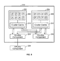
- FIG. 2B illustrates an embodiment of a multi-cluster chip.
- chip 200 comprises two clusters, 202 and 204 .
- the two clusters include at least one cluster of FIG. 2A .
- the chip may comprise any number of two or more clusters.
- Each cluster includes multiple processors ( 206 and 208 respectively for each cluster) and at least one cluster cache ( 210 and 212 respectively for each cluster) used by the processors of each respective cluster.
- Multiple clusters on the chip are connected together through cluster communication network 214 .
- an electrically shared connection links more than two components together.
- an electrically non-shared (electrically unshared) connection links two components together.
- a electrically non-shared (electrically unshared) connection includes a unidirectional connection with a single driver.
- the cluster communication network comprises electrically non-shared connections between components of the multi-cluster chip.
- Dedicated on-chip unidirectional interconnects connect the components together, eliminating the need for tri-state buffers and time-multiplexed data transfer. For example, all out going data from a cluster travels on a different electrically non-shared interconnect from any incoming data to the cluster. Out going data from each cluster travels on a different electrically non-shared interconnect from any out going data of another cluster.
- the on-chip bus design has been simplified, and the available bandwidth can be larger compared to using a traditional shared bus.
- Other components may be a part of the cluster communication network, including any component related to data communication, data routing, coherency, memory control, and cache control.
- two chips, each with at least two clusters and a cluster communication network are connected together.
- any data that needs to be transferred amongst the clusters on the chip are communicated through the cluster communication network.
- Two example categories of communication between the clusters are coherency communication and message passing.
- coherency communication a coherency protocol may be used to keep data related to a same memory location residing in cluster caches of two more or clusters consistent. For example, many clusters can be reading and using data from the same memory location. If one cluster modifies the data that is to be maintained coherent, other clusters need to be informed about the modification of the data.
- the cluster that requests to modify the data that is to be maintained coherent may send out an “invalidate” command to other clusters using the data before modifying the data. When other clusters receive the “invalidate” command, the clusters need to re-obtain the modified data from the cluster which modified it before the data can be used again.
- At least one cache level in cluster cache 210 and 212 are coherent. Coherency may be maintained on at least a portion of data in the private cache level of each processor and/or on at least a portion of data in the cluster cache. When coherency is maintained only on the private cache level, coherency data traffic may be communicated.
- a cluster cache may be inclusive of at least one private cache level of processors associated with the cluster cache. For example, any data cached in a private level of a processor is also cached in a cache level associated with the cluster cache. When the cluster cache is inclusive of the private cache level, only cluster cache coherency data traffic needs to be sent between the clusters.
- Coherency traffic may grow proportionally with the number of clusters in a system and not necessarily with the number of processors in the system.
- Coherency of data in the private cache level of processors may be maintained by respective cluster cache of the private cache level.
- a cluster cache is only inclusive of data that is maintained coherent in the private cache level of processors. For example, instruction data in the private cache level is not maintained coherent and not included in the cluster level cache. In some embodiments, at least some data maintained coherently in the private cache level is not cached in the cluster cache.
- messages are sent by one cluster to one or more other clusters.
- the messages may contain any data to be shared between the clusters.
- messages to be passed are specified by the programmer.
- the cluster caches of clusters do not necessarily have to be coherent.
- FIG. 3 illustrates an embodiment of a multi-cluster chip including an electrically non-shared direct interconnect.
- Clusters 202 and 204 are connected to each other by uni-directional interconnects. As more clusters are added, each new cluster requires two connections (one for receiving data and one for sending data) to other clusters. This can amount to 2*(N ⁇ 1) total cluster connections for each cluster, where N is the total number of clusters. In some embodiments, not all clusters are directly connected to every other cluster. Some clusters may communicate with other clusters through another cluster. In some embodiments, the cluster are connected to other clusters using a combination of non-shared and shared interconnects.
- FIG. 4 illustrates an embodiment of a multi-cluster chip including an integrated switch.
- Cluster 202 is connected to communication interface 216 .
- Cluster 204 is connected to communication interface 218 .
- the communication interfaces are connected together though switch 220 . Any number of clusters and components can be connected to a communication interface.
- the switch routes data between various clusters and components either located on-chip or off-chip. More than one switch can exist on the chip. Many data routing components can comprise a single logical switch.
- cluster 202 sends data to cluster 204
- data is sent to communication interface 216 though an electrically non-shared interconnect.
- From communication interface 216 data is routed through switch 220 to communication interface 218 for delivery to cluster 204 through an electrically non-shared interconnect.
- Switch 220 is connected to on-chip component 221 and off-chip component 222 .
- the switch is connected to zero or more on-chip components.
- the switch also may be connected to zero or more off-chip components.
- the components can be any component associated with processing, routing, caching, and storing data, including memory controller, i/o interface, snoop tag component, duplicate tag component, directory controller, and chip-to-chip links. Communication between clusters and the components are routed through the switch. Communication between the components can be routed through the switch as well.
- a ring topology used instead of a switch.
- the ring topology may be a hierarchical ring topology.
- FIG. 5 illustrates an embodiment of a multi-cluster chip including on-chip components.
- Components can be any component associated with processing, routing, caching, and storing data.
- Cluster 202 and 204 are connected to on-chip component 224 and 226 through electrically non-shared interconnects.
- An on-chip component may be connected to any number of clusters and other on-chip components.
- Off-chip component 228 is connected to on-chip component 224 . Any number of off-chip components can be connected to an on-chip component. Any number of on-chip components and off-chip components can exist.
- Communication between the clusters passes through one or more on-chip components.
- the component may perform additional processing associated with the data passing from one cluster to one or more clusters.
- the components can be used to maintain cache coherence.
- a snoop tag component snoops memory traffic for accesses to memory that have been cached.
- the clusters may be connected to each other directly.
- FIG. 6A illustrates an embodiment of a multi-cluster chip including components connected in a unidirectional ring configuration.
- Cluster 206 , cluster 208 , on-chip component 226 , and on-chip component 228 are connected together thorough unidirectional electrically unshared connections. Data may travel only in one direction of the ring.
- a cluster may include only one input and one output connection to other clusters/components, wherein a cluster/component of the input connection is different from a cluster/component of the output connection.
- FIG. 6B illustrates an embodiment of a multi-cluster chip including components connected in a bidirectional ring configuration. Data may travel in both directions of the ring.
- a cluster/component may route data to other cluster/component in the ring connection.
- on-chip component 224 is connected to off-chip component 228 .
- the off-chip component is optional. In some embodiments, more off-chip components exist.
Landscapes
- Engineering & Computer Science (AREA)
- Theoretical Computer Science (AREA)
- Physics & Mathematics (AREA)
- General Engineering & Computer Science (AREA)
- General Physics & Mathematics (AREA)
- Memory System Of A Hierarchy Structure (AREA)
Abstract
Description
Claims (34)
Priority Applications (1)
| Application Number | Priority Date | Filing Date | Title |
|---|---|---|---|
| US11/250,149 US8990501B1 (en) | 2005-10-12 | 2005-10-12 | Multiple cluster processor |
Applications Claiming Priority (1)
| Application Number | Priority Date | Filing Date | Title |
|---|---|---|---|
| US11/250,149 US8990501B1 (en) | 2005-10-12 | 2005-10-12 | Multiple cluster processor |
Publications (1)
| Publication Number | Publication Date |
|---|---|
| US8990501B1 true US8990501B1 (en) | 2015-03-24 |
Family
ID=52683473
Family Applications (1)
| Application Number | Title | Priority Date | Filing Date |
|---|---|---|---|
| US11/250,149 Active 2026-02-04 US8990501B1 (en) | 2005-10-12 | 2005-10-12 | Multiple cluster processor |
Country Status (1)
| Country | Link |
|---|---|
| US (1) | US8990501B1 (en) |
Cited By (5)
| Publication number | Priority date | Publication date | Assignee | Title |
|---|---|---|---|---|
| US20130287019A1 (en) * | 2012-04-30 | 2013-10-31 | Nuvoton Technology Corporation | Routing circuit and circuit having the routing circuit |
| US20140164706A1 (en) * | 2012-12-11 | 2014-06-12 | Electronics & Telecommunications Research Institute | Multi-core processor having hierarchical cahce architecture |
| US10394712B2 (en) * | 2014-11-20 | 2019-08-27 | International Business Machines Corporation | Configuration based cache coherency protocol selection |
| US11461234B2 (en) * | 2017-09-05 | 2022-10-04 | Numascale As | Coherent node controller |
| CN118642984A (en) * | 2024-08-14 | 2024-09-13 | 山东浪潮科学研究院有限公司 | Data sharing method, device, equipment and medium |
Citations (27)
| Publication number | Priority date | Publication date | Assignee | Title |
|---|---|---|---|---|
| US5564035A (en) * | 1994-03-23 | 1996-10-08 | Intel Corporation | Exclusive and/or partially inclusive extension cache system and method to minimize swapping therein |
| US5694573A (en) * | 1994-12-05 | 1997-12-02 | International Business Machines Corporation | Shared L2 support for inclusion property in split L1 data and instruction caches |
| US5732209A (en) | 1995-11-29 | 1998-03-24 | Exponential Technology, Inc. | Self-testing multi-processor die with internal compare points |
| US5909699A (en) * | 1994-02-28 | 1999-06-01 | Intel Corporation | Method and apparatus for supporting read, write, and invalidation operations to memory which maintain cache consistency |
| US6101589A (en) | 1998-04-01 | 2000-08-08 | International Business Machines Corporation | High performance shared cache |
| US6108721A (en) * | 1998-06-29 | 2000-08-22 | Hewlett-Packard Company | Method and apparatus for ensuring data consistency between an i/o channel and a processor |
| US6253292B1 (en) * | 1997-08-22 | 2001-06-26 | Seong Tae Jhang | Distributed shared memory multiprocessor system based on a unidirectional ring bus using a snooping scheme |
| US20020073282A1 (en) | 2000-08-21 | 2002-06-13 | Gerard Chauvel | Multiple microprocessors with a shared cache |
| US20030009629A1 (en) * | 2001-07-06 | 2003-01-09 | Fred Gruner | Sharing a second tier cache memory in a multi-processor |
| US20030120877A1 (en) | 2001-12-20 | 2003-06-26 | Jahnke Steven R. | Embedded symmetric multiprocessor system |
| US6658539B2 (en) | 2001-10-16 | 2003-12-02 | International Business Machines Corporation | Super-coherent data mechanisms for shared caches in a multiprocessing system |
| US20040022107A1 (en) * | 2000-01-20 | 2004-02-05 | Palmchip Corporation | Unidirectional bus architecture for SoC applications |
| US20040088487A1 (en) * | 2000-06-10 | 2004-05-06 | Barroso Luiz Andre | Scalable architecture based on single-chip multiprocessing |
| US6738864B2 (en) | 2000-08-21 | 2004-05-18 | Texas Instruments Incorporated | Level 2 cache architecture for multiprocessor with task—ID and resource—ID |
| US20040117559A1 (en) * | 2002-12-16 | 2004-06-17 | Newisys, Inc. A Delaware Corporation | Methods and apparatus for canceling a memory data fetch |
| US20040117598A1 (en) * | 2002-12-12 | 2004-06-17 | International Business Machines Corp. | Method and data processing system for microprocessor communication in a cluster-based multi-processor wireless network |
| US20040268052A1 (en) * | 2003-06-27 | 2004-12-30 | Newisys, Inc., A Delaware Corporation | Methods and apparatus for sending targeted probes |
| US20050021871A1 (en) * | 2003-07-25 | 2005-01-27 | International Business Machines Corporation | Self-contained processor subsystem as component for system-on-chip design |
| US20050108717A1 (en) * | 2003-11-18 | 2005-05-19 | Hong Steve J. | Systems and methods for creating an application group in a multiprocessor system |
| US20050138230A1 (en) * | 2003-12-19 | 2005-06-23 | International Business Machines Corporation | Method, apparatus and program product for low latency I/O adapter queuing in a computer system |
| US20050182915A1 (en) * | 2004-02-12 | 2005-08-18 | Patrick Devaney | Chip multiprocessor for media applications |
| US20050193174A1 (en) * | 1999-11-09 | 2005-09-01 | Ibm Corporation | System bus read data transfers with data ordering control bits |
| US20060059315A1 (en) * | 2004-09-15 | 2006-03-16 | Broadcom Corporation | Nonuniform chip multiprocessor |
| US20060129777A1 (en) * | 2002-02-19 | 2006-06-15 | Hobson Richard F | Processor cluster architecture and associated parallel processing methods |
| US7085866B1 (en) * | 2002-02-19 | 2006-08-01 | Hobson Richard F | Hierarchical bus structure and memory access protocol for multiprocessor systems |
| US20060176890A1 (en) * | 2005-02-10 | 2006-08-10 | International Business Machines Corporation | Data processing system, method and interconnect fabric for improved communication in a data processing system |
| US20070038814A1 (en) * | 2005-08-10 | 2007-02-15 | International Business Machines Corporation | Systems and methods for selectively inclusive cache |
-
2005
- 2005-10-12 US US11/250,149 patent/US8990501B1/en active Active
Patent Citations (29)
| Publication number | Priority date | Publication date | Assignee | Title |
|---|---|---|---|---|
| US5909699A (en) * | 1994-02-28 | 1999-06-01 | Intel Corporation | Method and apparatus for supporting read, write, and invalidation operations to memory which maintain cache consistency |
| US5564035A (en) * | 1994-03-23 | 1996-10-08 | Intel Corporation | Exclusive and/or partially inclusive extension cache system and method to minimize swapping therein |
| US5694573A (en) * | 1994-12-05 | 1997-12-02 | International Business Machines Corporation | Shared L2 support for inclusion property in split L1 data and instruction caches |
| US5732209A (en) | 1995-11-29 | 1998-03-24 | Exponential Technology, Inc. | Self-testing multi-processor die with internal compare points |
| US6253292B1 (en) * | 1997-08-22 | 2001-06-26 | Seong Tae Jhang | Distributed shared memory multiprocessor system based on a unidirectional ring bus using a snooping scheme |
| US6101589A (en) | 1998-04-01 | 2000-08-08 | International Business Machines Corporation | High performance shared cache |
| US6108721A (en) * | 1998-06-29 | 2000-08-22 | Hewlett-Packard Company | Method and apparatus for ensuring data consistency between an i/o channel and a processor |
| US20050193174A1 (en) * | 1999-11-09 | 2005-09-01 | Ibm Corporation | System bus read data transfers with data ordering control bits |
| US20040022107A1 (en) * | 2000-01-20 | 2004-02-05 | Palmchip Corporation | Unidirectional bus architecture for SoC applications |
| US20040088487A1 (en) * | 2000-06-10 | 2004-05-06 | Barroso Luiz Andre | Scalable architecture based on single-chip multiprocessing |
| US6738864B2 (en) | 2000-08-21 | 2004-05-18 | Texas Instruments Incorporated | Level 2 cache architecture for multiprocessor with task—ID and resource—ID |
| US20020073282A1 (en) | 2000-08-21 | 2002-06-13 | Gerard Chauvel | Multiple microprocessors with a shared cache |
| US6751706B2 (en) | 2000-08-21 | 2004-06-15 | Texas Instruments Incorporated | Multiple microprocessors with a shared cache |
| US20030009629A1 (en) * | 2001-07-06 | 2003-01-09 | Fred Gruner | Sharing a second tier cache memory in a multi-processor |
| US20030120876A1 (en) * | 2001-07-06 | 2003-06-26 | David Hass | Ring based multi-processing system |
| US6658539B2 (en) | 2001-10-16 | 2003-12-02 | International Business Machines Corporation | Super-coherent data mechanisms for shared caches in a multiprocessing system |
| US20030120877A1 (en) | 2001-12-20 | 2003-06-26 | Jahnke Steven R. | Embedded symmetric multiprocessor system |
| US7085866B1 (en) * | 2002-02-19 | 2006-08-01 | Hobson Richard F | Hierarchical bus structure and memory access protocol for multiprocessor systems |
| US20060129777A1 (en) * | 2002-02-19 | 2006-06-15 | Hobson Richard F | Processor cluster architecture and associated parallel processing methods |
| US20040117598A1 (en) * | 2002-12-12 | 2004-06-17 | International Business Machines Corp. | Method and data processing system for microprocessor communication in a cluster-based multi-processor wireless network |
| US20040117559A1 (en) * | 2002-12-16 | 2004-06-17 | Newisys, Inc. A Delaware Corporation | Methods and apparatus for canceling a memory data fetch |
| US20040268052A1 (en) * | 2003-06-27 | 2004-12-30 | Newisys, Inc., A Delaware Corporation | Methods and apparatus for sending targeted probes |
| US20050021871A1 (en) * | 2003-07-25 | 2005-01-27 | International Business Machines Corporation | Self-contained processor subsystem as component for system-on-chip design |
| US20050108717A1 (en) * | 2003-11-18 | 2005-05-19 | Hong Steve J. | Systems and methods for creating an application group in a multiprocessor system |
| US20050138230A1 (en) * | 2003-12-19 | 2005-06-23 | International Business Machines Corporation | Method, apparatus and program product for low latency I/O adapter queuing in a computer system |
| US20050182915A1 (en) * | 2004-02-12 | 2005-08-18 | Patrick Devaney | Chip multiprocessor for media applications |
| US20060059315A1 (en) * | 2004-09-15 | 2006-03-16 | Broadcom Corporation | Nonuniform chip multiprocessor |
| US20060176890A1 (en) * | 2005-02-10 | 2006-08-10 | International Business Machines Corporation | Data processing system, method and interconnect fabric for improved communication in a data processing system |
| US20070038814A1 (en) * | 2005-08-10 | 2007-02-15 | International Business Machines Corporation | Systems and methods for selectively inclusive cache |
Non-Patent Citations (19)
| Title |
|---|
| "The Imapct of Shared-Cache Clustering in Small-Scale Shared-Memory Multiprocessors", by Nayfeh et al. (0-8186-7237-4/96, 1996 IEEE), pp. 74-84. * |
| Barroso et al., Piranha A Scalable Architecture Based on Single-Chip Multiprocessing, In Proceeding of the 27th Annual International Symposium on Computer Architecture, Jun. 2000. |
| Basak et al. (Designing Processor-cluster Based Systems: Interplay Between Cluster Organizations and Broadcasting Algorithms). Aug. 12-16, 1996, ISSN: 0190-3918 pp. 271-274. * |
| Bossen et al., POWER4 Systems: Design for Reliability, IBM Server Group, Austin TX. |
| Brian Case, Sun Makes MAJC with Mirrors, Dual On-Chip Mirror-Image Processor Cores Cooperate for High Performance, Oct. 25, 1999. |
| Definition of "point-to-point communication" from Microsoft Computer Dictionary, published 2002, pp. 2. * |
| Georgiou et al. (A programmable scalable platform for next-generation networking, pp. 1-20) copyright 2004, ISBN 0-12-198157-6. * |
| Gostin et al., The Architecture of the HP Superdome Shared-Memory Multiprocessor, 2005. |
| Hydra, A Next Generation Microarchitecture, http://www-hydra.stanford.edu/. |
| Lemieux et al. (Directional and Single-Driver Wires in FPGA Interconnect: ISBN: 0-7803-8652-3/04, published 2004), pp. 41-48. * |
| Lostcircuits, HP PA-8800 RISC Processor, SMP on One Chip, Oct. 19, 2001, http://www.lostcircuits.com/cpu/hp-pa8800/. |
| Luiz Andre Barroso, COMPAQ, Piranha: Designing a Scalable CMP-based System for Commercial Workloads, Apr. 27, 2001. |
| McNairy et al., Montecito-The Next Product in the Itanium® Processor Family, Aug. 24, 2004. |
| Peter N. Glaskowsky, IBM Raises Curtain on POWER5, Oct. 14, 2003. |
| Quinn Jacobson, Sun Microsystems, Ultra SPARC®, IV Processors. |
| Sun Microsystems, UltraSPARC IV, Detailed View, http://www.sun.com/processors/UltraSPARC-IV/details.xml. |
| Tendler et al., POWER4 System Microarchitecture, IBM, J Res & Dev, vol. 46, No. 1, Jan. 2002. |
| Tremblay et al., The MAJC Architecture: A Synthesis of Parallelism and Scalability, 2000 IEEE. |
| U.S. Appl. No. 10/908,587, filed May 18, 2005, Normoyle et al. |
Cited By (8)
| Publication number | Priority date | Publication date | Assignee | Title |
|---|---|---|---|---|
| US20130287019A1 (en) * | 2012-04-30 | 2013-10-31 | Nuvoton Technology Corporation | Routing circuit and circuit having the routing circuit |
| US9456256B2 (en) * | 2012-04-30 | 2016-09-27 | Nuvoton Technology Corporation | Routing circuit and circuit having the routing circuit |
| US20140164706A1 (en) * | 2012-12-11 | 2014-06-12 | Electronics & Telecommunications Research Institute | Multi-core processor having hierarchical cahce architecture |
| US10394712B2 (en) * | 2014-11-20 | 2019-08-27 | International Business Machines Corporation | Configuration based cache coherency protocol selection |
| US10402328B2 (en) * | 2014-11-20 | 2019-09-03 | International Business Machines Corporation | Configuration based cache coherency protocol selection |
| US10824565B2 (en) * | 2014-11-20 | 2020-11-03 | International Business Machines Corporation | Configuration based cache coherency protocol selection |
| US11461234B2 (en) * | 2017-09-05 | 2022-10-04 | Numascale As | Coherent node controller |
| CN118642984A (en) * | 2024-08-14 | 2024-09-13 | 山东浪潮科学研究院有限公司 | Data sharing method, device, equipment and medium |
Similar Documents
| Publication | Publication Date | Title |
|---|---|---|
| CN105706068B (en) | The storage network of route memory flow and I/O flow | |
| KR100465583B1 (en) | Non-uniform memory access(numa) data processing system that speculatively forwards a read request to a remote processing node and communication method in the system | |
| US7380102B2 (en) | Communication link control among inter-coupled multiple processing units in a node to respective units in another node for request broadcasting and combined response | |
| US7818388B2 (en) | Data processing system, method and interconnect fabric supporting multiple planes of processing nodes | |
| US7827357B2 (en) | Providing an inclusive shared cache among multiple core-cache clusters | |
| US6631448B2 (en) | Cache coherence unit for interconnecting multiprocessor nodes having pipelined snoopy protocol | |
| KR100308323B1 (en) | Non-uniform memory access (numa) data processing system having shared intervention support | |
| US8151059B2 (en) | Conflict detection and resolution in a multi core-cache domain for a chip multi-processor employing scalability agent architecture | |
| US6374331B1 (en) | Distributed directory cache coherence multi-processor computer architecture | |
| US20130111149A1 (en) | Integrated circuits with cache-coherency | |
| US20090006668A1 (en) | Performing direct data transactions with a cache memory | |
| US12019552B2 (en) | Low latency inter-chip communication mechanism in a multi-chip processing system | |
| US8990501B1 (en) | Multiple cluster processor | |
| US10437725B2 (en) | Master requesting missing segments of a cache line for which the master has coherence ownership | |
| JP2005141606A (en) | Multiprocessor system | |
| US11449489B2 (en) | Split transaction coherency protocol in a data processing system | |
| CN117667785A (en) | Data processing method, data processing device, electronic equipment and storage medium | |
| US7809004B2 (en) | Data processing system and processing unit having an address-based launch governor | |
| US10901902B2 (en) | Efficient inclusive cache management | |
| KR20060080186A (en) | Data processing system | |
| Ros et al. | Emc 2: Extending magny-cours coherence for large-scale servers | |
| US10489292B2 (en) | Ownership tracking updates across multiple simultaneous operations | |
| CN113687955B (en) | Digital circuit design method for efficiently processing cache consistency between GPU (graphics processing Unit) chips | |
| JP2002197047A (en) | Computer system having input/output read data arranged directly in processor local cache | |
| JP2009054000A (en) | Multiprocessor system and cache management method |
Legal Events
| Date | Code | Title | Description |
|---|---|---|---|
| AS | Assignment |
Owner name: AZUL SYSTEMS, INC., CALIFORNIA Free format text: ASSIGNMENT OF ASSIGNORS INTEREST;ASSIGNORS:SELLERS, SCOTT;TENE, GIL;REEL/FRAME:017199/0187 Effective date: 20051209 |
|
| STCF | Information on status: patent grant |
Free format text: PATENTED CASE |
|
| AS | Assignment |
Owner name: SILICON VALLEY BANK, CALIFORNIA Free format text: SECURITY INTEREST;ASSIGNOR:AZUL SYSTEMS, INC.;REEL/FRAME:037641/0665 Effective date: 20151203 |
|
| AS | Assignment |
Owner name: PARTNERS FOR GROWTH IV, L.P., CALIFORNIA Free format text: SECURITY INTEREST;ASSIGNOR:AZUL SYSTEMS, INC.;REEL/FRAME:037959/0694 Effective date: 20160229 |
|
| MAFP | Maintenance fee payment |
Free format text: PAYMENT OF MAINTENANCE FEE, 4TH YEAR, LARGE ENTITY (ORIGINAL EVENT CODE: M1551); ENTITY STATUS OF PATENT OWNER: LARGE ENTITY Year of fee payment: 4 |
|
| AS | Assignment |
Owner name: AZUL SYSTEMS, INC., CALIFORNIA Free format text: RELEASE BY SECURED PARTY;ASSIGNOR:PARTNERS FOR GROWTH IV, L.P.;REEL/FRAME:048411/0138 Effective date: 20190221 |
|
| AS | Assignment |
Owner name: GOLUB CAPITAL LLC, AS COLLATERAL AGENT, ILLINOIS Free format text: SECURITY INTEREST;ASSIGNOR:AZUL SYSTEMS, INC.;REEL/FRAME:052293/0121 Effective date: 20200401 Owner name: AZUL SYSTEMS, INC., CALIFORNIA Free format text: RELEASE BY SECURED PARTY;ASSIGNOR:SILICON VALLEY BANK;REEL/FRAME:052293/0869 Effective date: 20200401 |
|
| MAFP | Maintenance fee payment |
Free format text: PAYMENT OF MAINTENANCE FEE, 8TH YEAR, LARGE ENTITY (ORIGINAL EVENT CODE: M1552); ENTITY STATUS OF PATENT OWNER: LARGE ENTITY Year of fee payment: 8 |