US8988566B2 - Lens array for partitioned image sensor having color filters - Google Patents
Lens array for partitioned image sensor having color filters Download PDFInfo
- Publication number
- US8988566B2 US8988566B2 US13/570,449 US201213570449A US8988566B2 US 8988566 B2 US8988566 B2 US 8988566B2 US 201213570449 A US201213570449 A US 201213570449A US 8988566 B2 US8988566 B2 US 8988566B2
- Authority
- US
- United States
- Prior art keywords
- lens
- focal length
- image sensor
- curvature
- color filter
- Prior art date
- Legal status (The legal status is an assumption and is not a legal conclusion. Google has not performed a legal analysis and makes no representation as to the accuracy of the status listed.)
- Active, expires
Links
- 239000011521 glass Substances 0.000 claims abstract description 52
- 238000003384 imaging method Methods 0.000 claims description 26
- 238000000576 coating method Methods 0.000 claims description 21
- 235000012431 wafers Nutrition 0.000 description 34
- 238000000411 transmission spectrum Methods 0.000 description 12
- 239000011248 coating agent Substances 0.000 description 8
- 238000000034 method Methods 0.000 description 7
- 238000010586 diagram Methods 0.000 description 6
- 239000006059 cover glass Substances 0.000 description 5
- 230000005540 biological transmission Effects 0.000 description 4
- 239000000463 material Substances 0.000 description 4
- 230000003287 optical effect Effects 0.000 description 4
- 125000006850 spacer group Chemical group 0.000 description 2
- 238000001228 spectrum Methods 0.000 description 2
- 239000000758 substrate Substances 0.000 description 2
- 241000593989 Scardinius erythrophthalmus Species 0.000 description 1
- 230000003321 amplification Effects 0.000 description 1
- 238000006243 chemical reaction Methods 0.000 description 1
- 230000007423 decrease Effects 0.000 description 1
- 230000000694 effects Effects 0.000 description 1
- 238000002329 infrared spectrum Methods 0.000 description 1
- 238000012986 modification Methods 0.000 description 1
- 230000004048 modification Effects 0.000 description 1
- 238000003199 nucleic acid amplification method Methods 0.000 description 1
- 238000005192 partition Methods 0.000 description 1
- 238000005096 rolling process Methods 0.000 description 1
- 239000004065 semiconductor Substances 0.000 description 1
Images




Classifications
-
- H04N5/2254—
-
- H—ELECTRICITY
- H04—ELECTRIC COMMUNICATION TECHNIQUE
- H04N—PICTORIAL COMMUNICATION, e.g. TELEVISION
- H04N23/00—Cameras or camera modules comprising electronic image sensors; Control thereof
- H04N23/50—Constructional details
- H04N23/55—Optical parts specially adapted for electronic image sensors; Mounting thereof
-
- H01L27/14621—
-
- H01L27/14627—
-
- H—ELECTRICITY
- H04—ELECTRIC COMMUNICATION TECHNIQUE
- H04N—PICTORIAL COMMUNICATION, e.g. TELEVISION
- H04N25/00—Circuitry of solid-state image sensors [SSIS]; Control thereof
- H04N25/10—Circuitry of solid-state image sensors [SSIS]; Control thereof for transforming different wavelengths into image signals
- H04N25/11—Arrangement of colour filter arrays [CFA]; Filter mosaics
- H04N25/13—Arrangement of colour filter arrays [CFA]; Filter mosaics characterised by the spectral characteristics of the filter elements
- H04N25/134—Arrangement of colour filter arrays [CFA]; Filter mosaics characterised by the spectral characteristics of the filter elements based on three different wavelength filter elements
-
- H04N9/045—
-
- H—ELECTRICITY
- H10—SEMICONDUCTOR DEVICES; ELECTRIC SOLID-STATE DEVICES NOT OTHERWISE PROVIDED FOR
- H10F—INORGANIC SEMICONDUCTOR DEVICES SENSITIVE TO INFRARED RADIATION, LIGHT, ELECTROMAGNETIC RADIATION OF SHORTER WAVELENGTH OR CORPUSCULAR RADIATION
- H10F39/00—Integrated devices, or assemblies of multiple devices, comprising at least one element covered by group H10F30/00, e.g. radiation detectors comprising photodiode arrays
- H10F39/011—Manufacture or treatment of image sensors covered by group H10F39/12
- H10F39/026—Wafer-level processing
-
- H—ELECTRICITY
- H10—SEMICONDUCTOR DEVICES; ELECTRIC SOLID-STATE DEVICES NOT OTHERWISE PROVIDED FOR
- H10F—INORGANIC SEMICONDUCTOR DEVICES SENSITIVE TO INFRARED RADIATION, LIGHT, ELECTROMAGNETIC RADIATION OF SHORTER WAVELENGTH OR CORPUSCULAR RADIATION
- H10F39/00—Integrated devices, or assemblies of multiple devices, comprising at least one element covered by group H10F30/00, e.g. radiation detectors comprising photodiode arrays
- H10F39/80—Constructional details of image sensors
- H10F39/805—Coatings
- H10F39/8053—Colour filters
-
- H—ELECTRICITY
- H10—SEMICONDUCTOR DEVICES; ELECTRIC SOLID-STATE DEVICES NOT OTHERWISE PROVIDED FOR
- H10F—INORGANIC SEMICONDUCTOR DEVICES SENSITIVE TO INFRARED RADIATION, LIGHT, ELECTROMAGNETIC RADIATION OF SHORTER WAVELENGTH OR CORPUSCULAR RADIATION
- H10F39/00—Integrated devices, or assemblies of multiple devices, comprising at least one element covered by group H10F30/00, e.g. radiation detectors comprising photodiode arrays
- H10F39/80—Constructional details of image sensors
- H10F39/806—Optical elements or arrangements associated with the image sensors
-
- H—ELECTRICITY
- H10—SEMICONDUCTOR DEVICES; ELECTRIC SOLID-STATE DEVICES NOT OTHERWISE PROVIDED FOR
- H10F—INORGANIC SEMICONDUCTOR DEVICES SENSITIVE TO INFRARED RADIATION, LIGHT, ELECTROMAGNETIC RADIATION OF SHORTER WAVELENGTH OR CORPUSCULAR RADIATION
- H10F39/00—Integrated devices, or assemblies of multiple devices, comprising at least one element covered by group H10F30/00, e.g. radiation detectors comprising photodiode arrays
- H10F39/80—Constructional details of image sensors
- H10F39/806—Optical elements or arrangements associated with the image sensors
- H10F39/8063—Microlenses
-
- H01L27/14685—
-
- H—ELECTRICITY
- H10—SEMICONDUCTOR DEVICES; ELECTRIC SOLID-STATE DEVICES NOT OTHERWISE PROVIDED FOR
- H10F—INORGANIC SEMICONDUCTOR DEVICES SENSITIVE TO INFRARED RADIATION, LIGHT, ELECTROMAGNETIC RADIATION OF SHORTER WAVELENGTH OR CORPUSCULAR RADIATION
- H10F39/00—Integrated devices, or assemblies of multiple devices, comprising at least one element covered by group H10F30/00, e.g. radiation detectors comprising photodiode arrays
- H10F39/011—Manufacture or treatment of image sensors covered by group H10F39/12
- H10F39/024—Manufacture or treatment of image sensors covered by group H10F39/12 of coatings or optical elements
Definitions
- the present invention relates generally to image sensors, and more specifically, to a lens array for a partitioned image sensor having color filters.
- An image capture unit typically includes an image sensor and an imaging lens.
- the imaging lens focuses light onto the image sensor to form an image, and the image sensor converts the light into electric signals.
- the electric signals are output from the image capture unit to other units in a host electronic system or a subsystem.
- the electronic system may be a mobile phone, a computer, a digital camera or a medical device.
- image capture units are increasingly required to have lower profiles so that overall sizes of electronic systems including the image capture units can be reduced while at the same time not sacrifice quality in the optical images that are captured.
- the profile of an image capture unit may be associated with the distance from the bottom of image sensor to the top of the imaging lens.
- FIG. 1A is a schematic diagram of an image capture unit including an imaging lens and an image sensor.
- FIG. 1B is a schematic diagram of a low profile image capture unit including a low profile imaging lens and an image sensor.
- FIG. 2 illustrates one example of an image sensor having four partitioned areas in accordance with the teachings of the present invention.
- FIG. 3A is a cross-section illustrating two lenses having different focal lengths and two partitioned areas of one example of a low profile image capture unit in accordance with the teachings of the present invention.
- FIG. 3B is a cross-section illustrating two lenses having different radii of curvature and two partitioned areas of one example of a low profile image capture unit in accordance with the teachings of the present invention.
- FIG. 4 illustrates example transmission spectra of photo-resist materials for red, green, and blue filters.
- FIG. 5 illustrates one example of a 2 ⁇ 2 lens array for a partitioned image sensor in accordance with the teachings of the present invention.
- FIG. 6 illustrates one example of a 2 ⁇ 2 lens array on a partitioned image sensor in accordance with the teachings of the present invention.
- FIG. 7A illustrates a cross section of one example of a 2 ⁇ 2 lens array on a partitioned image sensor in accordance with the teachings of the present invention.
- FIG. 7B illustrates another cross section of one example of a 2 ⁇ 2 lens array on a partitioned image sensor in accordance with the teachings of the present invention.
- FIG. 8A illustrates an example combined transmission spectrum of an IR-cut filter and red color filter in accordance with the teachings of the present invention.
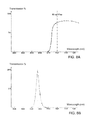
- FIG. 8B illustrates an example transmission spectrum of a green color filter in accordance with the teachings of the present invention.
- FIG. 8C illustrates an example transmission spectrum of blue color filter in accordance with the teachings of the present invention.
- FIG. 8D illustrates an example daylight spectrum transmitted through a UV-IR-cut filter in accordance with the teachings of the present invention.
- FIG. 8E illustrates an example transmission spectra of UV-IR-cut filter for 0°, 25°, 30°, and 35° incident light in accordance with the teachings of the present invention.
- FIG. 9 illustrates example transmission spectra of multilayer dielectric coatings red, green, and blue bandpass filters in accordance with the teachings of the present invention.
- FIG. 10 illustrates the cross section of a lens cube of a lens array on a partitioned image sensor in accordance with the teachings of the present invention.
- FIG. 11 is a block diagram illustrating one example of an image sensor in accordance with the teachings of the present invention.
- a low profile image capture unit may include an array of lenses having individual filters disposed on a partitioned image sensor.
- the quality of optical images captured which may for example be express in terms of resolution (i.e., the number of pixels) and/or sharpness, is not sacrificed for the low profile in accordance with the teachings of the present invention.
- FIG. 1A is a schematic diagram of an image capture unit 200 including an imaging lens 202 and an image sensor 204 .
- the distance between lens 202 and image sensor 204 is approximately f, where f is the focal length of lens 202 .
- the width of the image sensor 204 covered by lens 202 is W, and the lens diameter is D.
- FIG. 1B shows a schematic diagram of a low profile image capture unit 210 including an imaging lens 212 and an image sensor 214 .
- the distance between lens 212 and image sensor 214 is approximately f/2, where f/2 is the focal length of lens 212 .
- the width of the image sensor 214 covered by lens 212 is W/2, and the lens diameter is D/2.
- Image sensors 204 and 214 are the same image sensor, and both image sensors have the same pixel array structure. Since the width of image sensor 214 is half of the width of image sensor 204 , image sensor 214 will have half of number of pixels as compared with image sensor 204 in one dimension. In two dimensions, image sensor 214 will have quarter of number of pixels as compared with image sensor 204 . In other words, the number of pixels of the image captured is approximately proportional to the square of the scale of the distance between the lens and the image sensor.
- FIG. 2 illustrates an image sensor 220 having four partitioned areas 222 , 224 , 226 , and 228 closely arranged proximate to each other in accordance with the teachings of the present invention.
- Each partitioned area 222 , 224 , 226 , and 228 is covered by a respective imaging lens (e.g., lens 212 of FIG. 1B ).
- the focal length of the imaging lens e.g., lens 212 of FIG. 1B
- the focal length of the imaging lens can be half of the imaging lens when the image sensor is not partitioned into four areas (e.g., lens 202 of FIG. 1A ).
- a low profile image capture unit can be constructed using four lenses and four partitioned areas of an image sensor.
- the low profile image capture unit will have approximately the same resolution (i.e., the same number of pixels) as compared with the original image capture unit, because four areas of image sensor are used.
- An area of image sensor may be similar to image sensor 214 of FIG
- FIG. 3A shows a cross-section of low profile image capture unit 300 including four imaging lenses and four partitioned areas of image sensor in accordance with the teachings of the present invention.
- the cross-section illustrated in FIG. 3A may correspond with dashed line A-A′ of FIG. 2 .
- the four partitioned areas of image sensor may be areas 222 , 224 , 226 , and 228 of image sensor 220 of FIG. 2 .
- FIG. 3A Only two partitioned areas 222 and 224 of image sensor 220 are shown in FIG. 3A .
- an image capture system having low profile can be constructed, while the resolution (i.e., the number of pixels) of images captured can be maintained.
- imaging lens 302 is positioned a first focal length f 1 away from respective image sensor 222 .
- Imaging lens 304 is positioned a second focal length f 2 away from respective image sensor 224 .
- the second focal length f 2 is approximately half of the focal length when compared with lens 202 shown in FIG. 1A .
- example image capture unit 300 of FIG. 3A is a low profile image capture unit such that the width of the image sensors 222 and 224 covered by lens 302 and 304 are W/2, and the lens diameters of lenses 302 and 304 are D/2 in accordance with the teachings of the present invention.
- a typical image capture unit may include a Bayer type color filter array on the image sensor.
- Bayer type color filter array is typically made from photo-resist materials.
- the transmission spectra of photo-resist materials for red (R), green (G), and blue (B) filters are depicted in FIG. 4 .
- the transmission of red filter includes an IR spectrum, e.g., wavelength beyond 650 nm.
- an IR-cut filter is generally required to cut the transmission of wavelength beyond 650 nm.
- crosstalk domains in FIG. 4 that may degrade the quality of the color image.
- partitioned areas of image sensor 222 and 224 of FIG. 3A may not include Bayer type color filter array.
- partitioned areas 222 , 224 , 226 , and 228 may be designated to red (R), green (G), clear (C), and blue (B) areas, respectively.
- Red area may be covered by a single red filter
- green area may be covered by a single green filter
- blue area may be covered by a single blue filter
- clear or C area may not be covered by any filter or may be covered by a single green filter.
- Bayer type color filter array on the image sensor is based on a semiconductor lithographic process requiring very accurate overlay as sensor pitch decreases.
- the Bayer type color filter coating is a very expensive process.
- rework process will increase risk of damaging the image sensor.
- the single color filter coating on a glass substrate e.g., a glass wafer of a wafer-level lens cube, is an inexpensive process without necessity of accurate mask and alignment. Rework on glass substrate is very easy.
- the first focal length f 1 may be different than the second focal length f 2 .
- the first focal length f 1 corresponds with light having a first color, such as for example but not limited to red (R)
- second focal length f 2 corresponds with light having a second color, such as for example but not limited to green (G).
- R red
- G green
- a single image having the first color is focused by lens 302 onto image sensor 222 and the same single image having the second color is focused by lens 304 onto image sensor 224 in accordance with the teachings of the present invention.
- the red (R) area includes red pixels only
- the green (G) area includes green pixels only
- the blue (B) area includes blue pixels only.
- the clear or C area may include white pixels when no filter is applied, and green pixels when a green filter is applied.
- a readout system and/or processor may rearrange red, green, and blue pixels into Bayer pattern or any pattern for further processing the color signals and forming the color images.
- C pixels may be use as white pixels for particular processing or simply contribute as green pixels in accordance with the teachings of the present invention.
- FIG. 5 illustrates a lens array 400 for the partitioned image sensor in accordance with the teachings of the present invention.
- the partitioned image sensor may be image sensor 220 of FIG. 2 .
- Lens array 400 may be a 2 ⁇ 2 array having low profile lenses 402 , 404 , 406 , and 408 , which are designated to red (R), green (G), clear (C), and blue (B) areas, respectively.
- each one of the lenses 402 , 404 , 406 , and 408 is arranged to focus a single image onto a respective one of the red (R), green (G), clear (C), and blue (B) areas image sensor regions.
- lens 402 forms a red image only
- lens 404 forms a green image only
- lens 408 forms a blue image only.
- each one of the lenses 402 , 404 , 406 , and 408 has a different respective focal length that corresponds with the specific color of light that is being focused onto the corresponding image sensor region (e.g., see FIG. 3A ).
- each one of the lenses 402 , 404 , 406 , and 408 has a different respective radius of curvature (ROC) that corresponds with the specific color of light that is being focused onto the corresponding image sensor region (e.g., see FIG. 3B ).
- lenses 402 , 404 , 406 , and 408 may have the same focal length and the same ROC.
- FIG. 3B shows a cross-section of low profile image capture unit 320 including four imaging lenses and four partitioned areas of image sensor in accordance with the teachings of the present invention.
- the cross-section illustrated in FIG. 3B may correspond with dashed line A-A′ of FIG. 2 .
- the ROC of lenses 402 and 404 are different such that the focal lengths of lenses 402 and 404 become the same.
- each lens 402 , 404 , 406 , and 408 at individual color may be the same, and thus no individual adjustment of the focal length distance between each lens and the corresponding image sensor is necessary, in accordance with the teachings of the present invention. While the radii of curvature of R, G, and B lenses are different, the ROC of C lens 406 may be the same with one of lenses 402 , 404 , and 408 .
- lenses 402 , 404 , 406 , and 408 may have the same ROC, and the focal length difference of lenses 402 , 404 , 406 , and 408 may be small and negligible, in accordance with the teachings of the present invention (e.g., see FIGS. 7A and 7B ).
- FIG. 7A illustrates an example including the cross-section 550 of 2 ⁇ 2 lens array 500 in accordance with the teachings of the present invention. Only lens cubes 502 and 504 are shown in FIG. 7A .
- the cross-section illustrated in FIG. 7A may correspond with dashed line B-B′ of FIG. 6 .
- lens cubes 502 and 504 are disposed on a cover glass 510 .
- Partitioned areas 512 and 514 of a single image sensor are under cover glass 510 , aligned with lens cubes 502 and 504 , respectively.
- each wafer-level lens cube includes at least a glass wafer and a lens on the glass wafer.
- each wafer-level lens cube may include a lens 520 on a glass wafer 522 , a lens 524 on the other side of glass wafer 522 , a lens 528 on a glass wafer 530 , a lens 532 on the other side of glass wafer 530 , glass wafers 522 and 530 , a spacer 526 between glass wafers 522 and 530 , and a spacer 518 between glass wafer 530 and cover glass 510 .
- an IR-cut filter 702 is disposed on a glass wafer 562 underneath a lens 560 .
- IR-cut filter 702 may be multilayer dielectric coatings.
- the multilayer dielectric coatings may include alternate layers of high and low refractive indexes.
- a red color filter 704 is disposed in contact with the other side of glass wafer 562 between glass wafer 562 and a lens 564 .
- Red color filter 704 may be a photo-resist coating.
- the combined transmission spectrum of IR-cut filter 702 and red color filter 704 is depicted in FIG. 8A . In one example, the transmission of wavelengths beyond 650 nm will be cut by IR-cut filter 702 .
- Green color filter 706 is disposed in contact with glass wafer 522 between glass wafer 522 and lens 524 .
- Green color filter 706 may be a photo-resist coating.
- the transmission spectrum of green color filter 706 is depicted in FIG. 8B .
- IR-cut filter 702 and red filter 704 may be formed on either side of glass wafer 562 . Furthermore, IR-cut filter 702 and red filter 704 may be formed on either side of a second glass wafer 566 . Similarly, green filter 706 may be formed on either side of glass wafer 522 , or either side of second glass wafer 530 , in accordance with the teachings of the present invention.
- FIG. 7B illustrates the cross-section 600 of 2 ⁇ 2 lens array 500 in accordance with the teachings of the present invention. Only lens cubes 506 and 508 are shown in FIG. 7B .
- the cross-section illustrated in FIG. 7B may correspond with dashed line C-C′ of FIG. 6 .
- lens cubes 506 and 508 are disposed on a cover glass 510 .
- Partitioned areas 612 and 614 of a single image sensor are under cover glass 510 , aligned with lens cubes 506 and 508 , respectively.
- a blue color filter 708 is disposed in contact with a glass wafer 662 between glass wafer 662 and a lens 664 .
- Blue color filter 708 may be a photo-resist coating.
- the transmission spectrum of blue color filter 708 is depicted in FIG. 8C .
- a UV-IR-cut filter 710 is disposed on a glass wafer 622 underneath a lens 620 .
- UV-IR-cut filter 710 may be multilayer dielectric coatings.
- the multilayer dielectric coatings may include 30 alternate layers of high and low refractive indexes.
- the daylight spectrum transmitted through UV-IR-cut filter 710 is depicted in FIG. 8D .
- UV-IR-cut filter 710 The transmission spectra of UV-IR-cut filter 710 for 0°, 25°, 30°, and 35° incident light are depicted in FIG. 8E .
- UV-IR-cut filter cuts the transmissions of wavelengths longer than 650 nm and shorter than 420 nm.
- Blue filter 708 may be formed on either side of glass wafer 662 , or either side of a second glass wafer 666 .
- UV-IR-cut filter 710 may be formed on either side of glass wafer 622 , or either side of a second glass wafer 630 , in accordance with the teachings of the present invention.
- R lens cube 502 requires an IR-cut filter.
- G lens cube 504 and B lens cube 506 require no IR-cut filter.
- C lens cube 508 uses a combined UV-IR-cut filter and no individual IR-cut filter is required.
- photo-resist coating red filter 704 , green filter 706 , and blue filter 708 are replaced with multilayer dielectric coated red filter 724 , green filter 726 , and blue filter 728 , respectively, as depicted in FIGS. 7A and 7B , in accordance with the teachings of the present invention.
- the multilayer dielectric coated filters are bandpass filters.
- the transmission spectra of multilayer dielectric coated red filter 724 , green filter 726 , and blue filter 728 are shown in FIG. 9 .
- a multilayer dielectric coated color filter may include alternate layers of high and low refractive indexes.
- red filter 724 is a bandpass filter
- an IR-cut filter e.g., IR-cut filter 702
- the bandpass filters will also alleviate the crosstalk of photo-resist filters as shown in FIG. 4 .
- the IR-cut filter, the UV-IR-cut filter, and the red, green, and blue filters may appropriately be coated as a filter 902 over a lens 960 on a glass wafer 962 and over the surface of glass wafer 962 surrounding lens 960 , or a filter 904 over a lens 964 on the other side of glass wafer 962 and over the surface on glass wafer 962 surrounding lens 964 as depicted in FIG. 10 , in accordance with the teachings of the present invention.
- FIG. 10 shows a lens cube 900 , which may be one of lens cubes depicted in FIGS. 7A and 7B .
- FIG. 11 is a block diagram illustrating an image sensor 800 , in accordance with the teachings of the present invention.
- Image sensor 800 is one example implementation of image sensor 220 of FIG. 2 , or image sensor 501 of FIG. 6 .
- the illustrated example of image sensor 800 includes a pixel array 805 , readout circuitry 810 , function logic 815 , and control circuitry 820 .
- Pixel array 805 may be partitioned into four partitioned areas such as shown in FIG. 2 (not shown in FIG. 11 ).
- Pixel array 805 is a two-dimensional (2D) array of an image sensor or pixels (e.g., pixels P 1 , P 2 , . . . , Pn). Each pixel may be a CMOS pixel or a CCD pixel. As illustrated, each pixel is arranged into a row (e.g., rows R 1 to Ry) and a column (e.g., column C 1 to Cx) to acquire image data of a person, place, object, etc., which can then be used to render a 2D image of the person, place, object, etc. In one example, pixel array 805 is a backside illuminated (BSI) image sensor. In one example, pixel array 805 is a frontside illuminated (FSI) image example, pixel array 805 is partitioned into a plurality of partitioned areas. Each partitioned area is covered by a color filter.
- BSI backside illuminated
- FSI frontside illuminated
- Readout circuitry 810 may include amplification circuitry, analog-to-digital (ADC) conversion circuitry, or otherwise.
- Function logic 815 may simply store the image data or even manipulate the image data by applying post image effects (e.g., crop, rotate, remove red eye, adjust brightness, adjust contrast, or otherwise).
- readout circuitry 810 may readout a row of image data at a time along readout column lines (illustrated) or may readout the image data using a variety of other techniques (not illustrated), such as a serial readout or a full parallel readout of all pixels simultaneously.
- Control circuitry 820 is coupled to pixel array 805 to control operational characteristic of pixel array 805 .
- control circuitry 820 may generate a shutter signal for controlling image acquisition.
- the shutter signal is a global shutter signal for simultaneously enabling all pixels within pixel array 805 to simultaneously capture their respective image data during a single acquisition window.
- the shutter signal is a rolling shutter signal whereby each row, column, or group of pixels is sequentially enabled during consecutive acquisition windows.
- the low profile image capture unit is not limited to 2 ⁇ 2 lens array, any size of lens array is possible. Accordingly, the image sensor is not limited to four partitioned areas, any number of partitioned areas is possible.
- the partitioned area of image sensor may be square or rectangular.
- the cross section of lens cube may be circular, ellipse, square, or rectangular.
- the image sensor may be a CMOS image sensor or a CCD.
Landscapes
- Engineering & Computer Science (AREA)
- Multimedia (AREA)
- Signal Processing (AREA)
- Physics & Mathematics (AREA)
- Spectroscopy & Molecular Physics (AREA)
- Solid State Image Pick-Up Elements (AREA)
- Color Television Image Signal Generators (AREA)
- Facsimile Heads (AREA)
Priority Applications (4)
| Application Number | Priority Date | Filing Date | Title |
|---|---|---|---|
| US13/570,449 US8988566B2 (en) | 2012-08-09 | 2012-08-09 | Lens array for partitioned image sensor having color filters |
| TW102124070A TWI549273B (zh) | 2012-08-09 | 2013-07-04 | 用於具彩色濾光片之分割影像感測器之鏡片陣列 |
| CN201310313751.4A CN103579268B (zh) | 2012-08-09 | 2013-07-24 | 具有色彩滤光器的分割图像传感器的透镜阵列 |
| EP13179183.2A EP2696570B1 (de) | 2012-08-09 | 2013-08-02 | Linsenanordnung für partitionierten Bildsensor mit Farbfiltern |
Applications Claiming Priority (1)
| Application Number | Priority Date | Filing Date | Title |
|---|---|---|---|
| US13/570,449 US8988566B2 (en) | 2012-08-09 | 2012-08-09 | Lens array for partitioned image sensor having color filters |
Publications (2)
| Publication Number | Publication Date |
|---|---|
| US20140043507A1 US20140043507A1 (en) | 2014-02-13 |
| US8988566B2 true US8988566B2 (en) | 2015-03-24 |
Family
ID=49083514
Family Applications (1)
| Application Number | Title | Priority Date | Filing Date |
|---|---|---|---|
| US13/570,449 Active 2033-07-03 US8988566B2 (en) | 2012-08-09 | 2012-08-09 | Lens array for partitioned image sensor having color filters |
Country Status (4)
| Country | Link |
|---|---|
| US (1) | US8988566B2 (de) |
| EP (1) | EP2696570B1 (de) |
| CN (1) | CN103579268B (de) |
| TW (1) | TWI549273B (de) |
Cited By (3)
| Publication number | Priority date | Publication date | Assignee | Title |
|---|---|---|---|---|
| US20150281601A1 (en) * | 2014-03-25 | 2015-10-01 | INVIS Technologies Corporation | Modular Packaging and Optical System for Multi-Aperture and Multi-Spectral Camera Core |
| US11366011B2 (en) | 2019-02-13 | 2022-06-21 | Viavi Solutions Inc. | Optical device |
| JP2022535238A (ja) * | 2019-06-06 | 2022-08-05 | アプライド マテリアルズ インコーポレイテッド | 撮像システム及び合成画像を生成する方法 |
Families Citing this family (63)
| Publication number | Priority date | Publication date | Assignee | Title |
|---|---|---|---|---|
| US11792538B2 (en) | 2008-05-20 | 2023-10-17 | Adeia Imaging Llc | Capturing and processing of images including occlusions focused on an image sensor by a lens stack array |
| EP3328048B1 (de) | 2008-05-20 | 2021-04-21 | FotoNation Limited | Aufnahme und verarbeitung von bildern mittels monolithischer kamera anordnung mit heterogenem bildwandler |
| US8866920B2 (en) | 2008-05-20 | 2014-10-21 | Pelican Imaging Corporation | Capturing and processing of images using monolithic camera array with heterogeneous imagers |
| EP2502115A4 (de) | 2009-11-20 | 2013-11-06 | Pelican Imaging Corp | Aufnahme und verarbeitung von bildern mittels eines monolithischen kameraarrays mit heterogenem bildwandler |
| CN103004180A (zh) | 2010-05-12 | 2013-03-27 | 派力肯影像公司 | 成像器阵列和阵列照相机的架构 |
| US8878950B2 (en) | 2010-12-14 | 2014-11-04 | Pelican Imaging Corporation | Systems and methods for synthesizing high resolution images using super-resolution processes |
| US8305456B1 (en) | 2011-05-11 | 2012-11-06 | Pelican Imaging Corporation | Systems and methods for transmitting and receiving array camera image data |
| US20130265459A1 (en) | 2011-06-28 | 2013-10-10 | Pelican Imaging Corporation | Optical arrangements for use with an array camera |
| WO2013043751A1 (en) | 2011-09-19 | 2013-03-28 | Pelican Imaging Corporation | Systems and methods for controlling aliasing in images captured by an array camera for use in super resolution processing using pixel apertures |
| CN104081414B (zh) | 2011-09-28 | 2017-08-01 | Fotonation开曼有限公司 | 用于编码和解码光场图像文件的系统及方法 |
| US9412206B2 (en) | 2012-02-21 | 2016-08-09 | Pelican Imaging Corporation | Systems and methods for the manipulation of captured light field image data |
| US9210392B2 (en) | 2012-05-01 | 2015-12-08 | Pelican Imaging Coporation | Camera modules patterned with pi filter groups |
| US8791403B2 (en) * | 2012-06-01 | 2014-07-29 | Omnivision Technologies, Inc. | Lens array for partitioned image sensor to focus a single image onto N image sensor regions |
| EP2873028A4 (de) | 2012-06-28 | 2016-05-25 | Pelican Imaging Corp | Systeme und verfahren zur erkennung defekter kamera-arrays, optischer arrays und sensoren |
| US20140002674A1 (en) | 2012-06-30 | 2014-01-02 | Pelican Imaging Corporation | Systems and Methods for Manufacturing Camera Modules Using Active Alignment of Lens Stack Arrays and Sensors |
| CN107346061B (zh) | 2012-08-21 | 2020-04-24 | 快图有限公司 | 用于使用阵列照相机捕捉的图像中的视差检测和校正的系统和方法 |
| EP2888698A4 (de) | 2012-08-23 | 2016-06-29 | Pelican Imaging Corp | Eigenschaftsbasierte hochauflösende bewegungsschätzung aus mit einer arrayquelle aufgenommenen niedrigauflösenden bildern |
| WO2014052974A2 (en) | 2012-09-28 | 2014-04-03 | Pelican Imaging Corporation | Generating images from light fields utilizing virtual viewpoints |
| US9143711B2 (en) | 2012-11-13 | 2015-09-22 | Pelican Imaging Corporation | Systems and methods for array camera focal plane control |
| US9462164B2 (en) | 2013-02-21 | 2016-10-04 | Pelican Imaging Corporation | Systems and methods for generating compressed light field representation data using captured light fields, array geometry, and parallax information |
| US9253380B2 (en) | 2013-02-24 | 2016-02-02 | Pelican Imaging Corporation | Thin form factor computational array cameras and modular array cameras |
| US9774789B2 (en) | 2013-03-08 | 2017-09-26 | Fotonation Cayman Limited | Systems and methods for high dynamic range imaging using array cameras |
| US8866912B2 (en) | 2013-03-10 | 2014-10-21 | Pelican Imaging Corporation | System and methods for calibration of an array camera using a single captured image |
| US9519972B2 (en) | 2013-03-13 | 2016-12-13 | Kip Peli P1 Lp | Systems and methods for synthesizing images from image data captured by an array camera using restricted depth of field depth maps in which depth estimation precision varies |
| US9124831B2 (en) | 2013-03-13 | 2015-09-01 | Pelican Imaging Corporation | System and methods for calibration of an array camera |
| US9888194B2 (en) | 2013-03-13 | 2018-02-06 | Fotonation Cayman Limited | Array camera architecture implementing quantum film image sensors |
| US9106784B2 (en) | 2013-03-13 | 2015-08-11 | Pelican Imaging Corporation | Systems and methods for controlling aliasing in images captured by an array camera for use in super-resolution processing |
| WO2014153098A1 (en) | 2013-03-14 | 2014-09-25 | Pelican Imaging Corporation | Photmetric normalization in array cameras |
| WO2014159779A1 (en) | 2013-03-14 | 2014-10-02 | Pelican Imaging Corporation | Systems and methods for reducing motion blur in images or video in ultra low light with array cameras |
| EP4604059A3 (de) | 2013-03-15 | 2025-09-17 | Adeia Imaging LLC | Systémes et procédés d'imagerie stéréo á l'aide des réseaux de caméras |
| US9497429B2 (en) | 2013-03-15 | 2016-11-15 | Pelican Imaging Corporation | Extended color processing on pelican array cameras |
| US10122993B2 (en) | 2013-03-15 | 2018-11-06 | Fotonation Limited | Autofocus system for a conventional camera that uses depth information from an array camera |
| US9445003B1 (en) | 2013-03-15 | 2016-09-13 | Pelican Imaging Corporation | Systems and methods for synthesizing high resolution images using image deconvolution based on motion and depth information |
| US10151859B2 (en) * | 2013-09-23 | 2018-12-11 | Lg Innotek Co., Ltd. | Camera module and manufacturing method for same |
| WO2015048694A2 (en) | 2013-09-27 | 2015-04-02 | Pelican Imaging Corporation | Systems and methods for depth-assisted perspective distortion correction |
| CN103557459B (zh) * | 2013-11-06 | 2016-03-02 | 郑州中原显示技术有限公司 | 发光面不相同的三基色led灯 |
| US9426343B2 (en) | 2013-11-07 | 2016-08-23 | Pelican Imaging Corporation | Array cameras incorporating independently aligned lens stacks |
| US10119808B2 (en) | 2013-11-18 | 2018-11-06 | Fotonation Limited | Systems and methods for estimating depth from projected texture using camera arrays |
| EP3075140B1 (de) | 2013-11-26 | 2018-06-13 | FotoNation Cayman Limited | Zeilenkamerakonfigurationen mit mehreren zeilenkameras |
| US10089740B2 (en) | 2014-03-07 | 2018-10-02 | Fotonation Limited | System and methods for depth regularization and semiautomatic interactive matting using RGB-D images |
| US9270953B2 (en) * | 2014-05-16 | 2016-02-23 | Omnivision Technologies, Inc. | Wafer level camera having movable color filter grouping |
| US9521319B2 (en) * | 2014-06-18 | 2016-12-13 | Pelican Imaging Corporation | Array cameras and array camera modules including spectral filters disposed outside of a constituent image sensor |
| CN113256730B (zh) | 2014-09-29 | 2023-09-05 | 快图有限公司 | 用于阵列相机的动态校准的系统和方法 |
| US9942474B2 (en) | 2015-04-17 | 2018-04-10 | Fotonation Cayman Limited | Systems and methods for performing high speed video capture and depth estimation using array cameras |
| CN105223756B (zh) * | 2015-10-06 | 2018-03-09 | 瑞声光电科技(常州)有限公司 | 阵列式镜头模组 |
| US10313642B2 (en) * | 2017-01-18 | 2019-06-04 | Omnivision Technologies, Inc. | Imaging system having dual image sensors |
| US10482618B2 (en) | 2017-08-21 | 2019-11-19 | Fotonation Limited | Systems and methods for hybrid depth regularization |
| WO2021055585A1 (en) | 2019-09-17 | 2021-03-25 | Boston Polarimetrics, Inc. | Systems and methods for surface modeling using polarization cues |
| WO2021071995A1 (en) | 2019-10-07 | 2021-04-15 | Boston Polarimetrics, Inc. | Systems and methods for surface normals sensing with polarization |
| EP4066001B1 (de) | 2019-11-30 | 2026-03-04 | Intrinsic Innovation LLC | Systeme und verfahren zur transparenten objektsegmentierung unter verwendung von polarisationshinweisen |
| JP7462769B2 (ja) | 2020-01-29 | 2024-04-05 | イントリンジック イノベーション エルエルシー | 物体の姿勢の検出および測定システムを特徴付けるためのシステムおよび方法 |
| US11797863B2 (en) | 2020-01-30 | 2023-10-24 | Intrinsic Innovation Llc | Systems and methods for synthesizing data for training statistical models on different imaging modalities including polarized images |
| WO2021243088A1 (en) | 2020-05-27 | 2021-12-02 | Boston Polarimetrics, Inc. | Multi-aperture polarization optical systems using beam splitters |
| US12069227B2 (en) | 2021-03-10 | 2024-08-20 | Intrinsic Innovation Llc | Multi-modal and multi-spectral stereo camera arrays |
| US12020455B2 (en) | 2021-03-10 | 2024-06-25 | Intrinsic Innovation Llc | Systems and methods for high dynamic range image reconstruction |
| US11954886B2 (en) | 2021-04-15 | 2024-04-09 | Intrinsic Innovation Llc | Systems and methods for six-degree of freedom pose estimation of deformable objects |
| US11290658B1 (en) | 2021-04-15 | 2022-03-29 | Boston Polarimetrics, Inc. | Systems and methods for camera exposure control |
| US12067746B2 (en) | 2021-05-07 | 2024-08-20 | Intrinsic Innovation Llc | Systems and methods for using computer vision to pick up small objects |
| US12175741B2 (en) | 2021-06-22 | 2024-12-24 | Intrinsic Innovation Llc | Systems and methods for a vision guided end effector |
| US12340538B2 (en) | 2021-06-25 | 2025-06-24 | Intrinsic Innovation Llc | Systems and methods for generating and using visual datasets for training computer vision models |
| US12172310B2 (en) | 2021-06-29 | 2024-12-24 | Intrinsic Innovation Llc | Systems and methods for picking objects using 3-D geometry and segmentation |
| US11689813B2 (en) | 2021-07-01 | 2023-06-27 | Intrinsic Innovation Llc | Systems and methods for high dynamic range imaging using crossed polarizers |
| US12293535B2 (en) | 2021-08-03 | 2025-05-06 | Intrinsic Innovation Llc | Systems and methods for training pose estimators in computer vision |
Citations (18)
| Publication number | Priority date | Publication date | Assignee | Title |
|---|---|---|---|---|
| EP1067802A2 (de) | 1999-06-30 | 2001-01-10 | Canon Kabushiki Kaisha | Farbbildaufnahmegerät |
| US20020089596A1 (en) | 2000-12-28 | 2002-07-11 | Yasuo Suda | Image sensing apparatus |
| US20060023314A1 (en) | 2004-07-27 | 2006-02-02 | Boettiger Ulrich C | Controlling lens shape in a microlens array |
| US20060226452A1 (en) | 2005-04-08 | 2006-10-12 | Konica Minolta Opto, Inc. | Solid-state image pickup device and the manufacture method thereof |
| US20070008421A1 (en) | 2005-07-07 | 2007-01-11 | Hsin-Ping Wu | Method for forming microlenses of different curvatures and fabricating process of solid-state image sensor |
| US20070126898A1 (en) * | 2004-09-27 | 2007-06-07 | Digital Optics Corporation | Thin camera and associated methods |
| US7247851B2 (en) | 2003-11-10 | 2007-07-24 | Matsushita Electric Industrial Co., Ltd. | Imaging device and an imaging method |
| US20080049126A1 (en) | 2006-08-28 | 2008-02-28 | Micron Technology, Inc. | Color filter array and method of fabrication and use |
| US20080128843A1 (en) | 2006-11-30 | 2008-06-05 | Lee Sang Uk | Image Sensor and Fabricating Method Thereof |
| US20080142685A1 (en) | 2006-12-13 | 2008-06-19 | Gazeley William G | Integrated image sensor having a color-filtering microlens, and related system and method |
| US7453510B2 (en) * | 2003-12-11 | 2008-11-18 | Nokia Corporation | Imaging device |
| US20100065897A1 (en) | 2008-09-16 | 2010-03-18 | Sung Ho Jun | CMOS Image Sensor and Method for Fabricating the Same |
| EP2214405A2 (de) | 2009-02-02 | 2010-08-04 | L-3 Communications Cincinnati Electronics | Mehrkanalbildgebungsvorrichtungen |
| US7812869B2 (en) | 2007-05-11 | 2010-10-12 | Aptina Imaging Corporation | Configurable pixel array system and method |
| US20110122308A1 (en) * | 2009-11-20 | 2011-05-26 | Pelican Imaging Corporation | Capturing and processing of images using monolithic camera array with heterogeneous imagers |
| US20110194019A1 (en) | 2010-02-11 | 2011-08-11 | San-Woei Shyu | Optical imaging lens and array thereof |
| US20120104525A1 (en) | 2008-02-11 | 2012-05-03 | Omnivision Technologies, Inc. | Image sensor with color pixels having uniform light absorption depths |
| US20130320195A1 (en) | 2012-06-01 | 2013-12-05 | Omnivision Technologies, Inc. | Lens array for partitioned image sensor |
Family Cites Families (1)
| Publication number | Priority date | Publication date | Assignee | Title |
|---|---|---|---|---|
| CN100474003C (zh) * | 2006-04-04 | 2009-04-01 | 精工爱普生株式会社 | 光学多层膜滤波器和电子设备装置 |
-
2012
- 2012-08-09 US US13/570,449 patent/US8988566B2/en active Active
-
2013
- 2013-07-04 TW TW102124070A patent/TWI549273B/zh active
- 2013-07-24 CN CN201310313751.4A patent/CN103579268B/zh active Active
- 2013-08-02 EP EP13179183.2A patent/EP2696570B1/de active Active
Patent Citations (18)
| Publication number | Priority date | Publication date | Assignee | Title |
|---|---|---|---|---|
| EP1067802A2 (de) | 1999-06-30 | 2001-01-10 | Canon Kabushiki Kaisha | Farbbildaufnahmegerät |
| US20020089596A1 (en) | 2000-12-28 | 2002-07-11 | Yasuo Suda | Image sensing apparatus |
| US7247851B2 (en) | 2003-11-10 | 2007-07-24 | Matsushita Electric Industrial Co., Ltd. | Imaging device and an imaging method |
| US7453510B2 (en) * | 2003-12-11 | 2008-11-18 | Nokia Corporation | Imaging device |
| US20060023314A1 (en) | 2004-07-27 | 2006-02-02 | Boettiger Ulrich C | Controlling lens shape in a microlens array |
| US20070126898A1 (en) * | 2004-09-27 | 2007-06-07 | Digital Optics Corporation | Thin camera and associated methods |
| US20060226452A1 (en) | 2005-04-08 | 2006-10-12 | Konica Minolta Opto, Inc. | Solid-state image pickup device and the manufacture method thereof |
| US20070008421A1 (en) | 2005-07-07 | 2007-01-11 | Hsin-Ping Wu | Method for forming microlenses of different curvatures and fabricating process of solid-state image sensor |
| US20080049126A1 (en) | 2006-08-28 | 2008-02-28 | Micron Technology, Inc. | Color filter array and method of fabrication and use |
| US20080128843A1 (en) | 2006-11-30 | 2008-06-05 | Lee Sang Uk | Image Sensor and Fabricating Method Thereof |
| US20080142685A1 (en) | 2006-12-13 | 2008-06-19 | Gazeley William G | Integrated image sensor having a color-filtering microlens, and related system and method |
| US7812869B2 (en) | 2007-05-11 | 2010-10-12 | Aptina Imaging Corporation | Configurable pixel array system and method |
| US20120104525A1 (en) | 2008-02-11 | 2012-05-03 | Omnivision Technologies, Inc. | Image sensor with color pixels having uniform light absorption depths |
| US20100065897A1 (en) | 2008-09-16 | 2010-03-18 | Sung Ho Jun | CMOS Image Sensor and Method for Fabricating the Same |
| EP2214405A2 (de) | 2009-02-02 | 2010-08-04 | L-3 Communications Cincinnati Electronics | Mehrkanalbildgebungsvorrichtungen |
| US20110122308A1 (en) * | 2009-11-20 | 2011-05-26 | Pelican Imaging Corporation | Capturing and processing of images using monolithic camera array with heterogeneous imagers |
| US20110194019A1 (en) | 2010-02-11 | 2011-08-11 | San-Woei Shyu | Optical imaging lens and array thereof |
| US20130320195A1 (en) | 2012-06-01 | 2013-12-05 | Omnivision Technologies, Inc. | Lens array for partitioned image sensor |
Non-Patent Citations (6)
| Title |
|---|
| EP 13167195.0-European Search Report and Search Opinion, dated Nov. 6, 2013 (11 pages). |
| EP 13167195.0—European Search Report and Search Opinion, dated Nov. 6, 2013 (11 pages). |
| EP 13179183.2-Extended European Search Report, dated Jul. 16, 2014 (7 pages). |
| EP 13179183.2—Extended European Search Report, dated Jul. 16, 2014 (7 pages). |
| TW Patent Application No. 102115760-First Taiwanese Office Action, issued Sep. 24, 2014, with Search Report and English Translation (14 pages). |
| TW Patent Application No. 102115760—First Taiwanese Office Action, issued Sep. 24, 2014, with Search Report and English Translation (14 pages). |
Cited By (4)
| Publication number | Priority date | Publication date | Assignee | Title |
|---|---|---|---|---|
| US20150281601A1 (en) * | 2014-03-25 | 2015-10-01 | INVIS Technologies Corporation | Modular Packaging and Optical System for Multi-Aperture and Multi-Spectral Camera Core |
| US11366011B2 (en) | 2019-02-13 | 2022-06-21 | Viavi Solutions Inc. | Optical device |
| US11913833B2 (en) | 2019-02-13 | 2024-02-27 | Viavi Solutions Inc. | Optical device |
| JP2022535238A (ja) * | 2019-06-06 | 2022-08-05 | アプライド マテリアルズ インコーポレイテッド | 撮像システム及び合成画像を生成する方法 |
Also Published As
| Publication number | Publication date |
|---|---|
| CN103579268B (zh) | 2016-09-07 |
| TWI549273B (zh) | 2016-09-11 |
| TW201407757A (zh) | 2014-02-16 |
| EP2696570A2 (de) | 2014-02-12 |
| CN103579268A (zh) | 2014-02-12 |
| US20140043507A1 (en) | 2014-02-13 |
| EP2696570A3 (de) | 2014-08-13 |
| EP2696570B1 (de) | 2019-07-17 |
Similar Documents
| Publication | Publication Date | Title |
|---|---|---|
| US8988566B2 (en) | Lens array for partitioned image sensor having color filters | |
| US8791403B2 (en) | Lens array for partitioned image sensor to focus a single image onto N image sensor regions | |
| US10297629B2 (en) | Image sensors with in-pixel lens arrays | |
| US9270953B2 (en) | Wafer level camera having movable color filter grouping | |
| US8530814B2 (en) | Solid-state imaging device with a planarized lens layer method of manufacturing the same, and electronic apparatus | |
| US10506187B2 (en) | Image sensor having dual microlenses for each auto-focus (AF) pixel | |
| WO2016114154A1 (ja) | 固体撮像素子およびその製造方法、並びに電子機器 | |
| US10021326B2 (en) | Solid-state image sensor including pixels for detecting focus using a difference in intensity between lights | |
| CN102881699A (zh) | 固态成像器件、固态成像器件的制造方法以及电子装置 | |
| US9386203B2 (en) | Compact spacer in multi-lens array module | |
| US20230395626A1 (en) | Hybrid image pixels for phase detection auto focus | |
| US9595551B2 (en) | Solid-state imaging device and electronic apparatus | |
| US8389921B2 (en) | Image sensor having array of pixels and metal reflectors with widths scaled based on distance from center of the array | |
| HK1192371A (en) | Lens array for partitioned image sensor having color filters | |
| HK1192371B (en) | Lens array for partitioned image sensor having color filters | |
| TW202412292A (zh) | 改善半四象限光電二極體(qpd)通道不平衡之半四象限光電二極體 | |
| HK1190253A (en) | Lens array for partitioned image sensor | |
| HK1190253B (en) | Lens array for partitioned image sensor | |
| HK1209551B (zh) | 多透鏡陣列模塊中的緊湊間隔件 | |
| HK1212840B (zh) | 具有可移動彩色濾光器群組的晶片級相機 |
Legal Events
| Date | Code | Title | Description |
|---|---|---|---|
| AS | Assignment |
Owner name: OMNIVISION TECHNOLOGIES, INC., CALIFORNIA Free format text: ASSIGNMENT OF ASSIGNORS INTEREST;ASSIGNORS:WANG, CHIA-CHING;DENG, JAU-JAN;HSU, YUN-CHIANG;REEL/FRAME:028756/0772 Effective date: 20120807 |
|
| STCF | Information on status: patent grant |
Free format text: PATENTED CASE |
|
| MAFP | Maintenance fee payment |
Free format text: PAYMENT OF MAINTENANCE FEE, 4TH YEAR, LARGE ENTITY (ORIGINAL EVENT CODE: M1551); ENTITY STATUS OF PATENT OWNER: LARGE ENTITY Year of fee payment: 4 |
|
| MAFP | Maintenance fee payment |
Free format text: PAYMENT OF MAINTENANCE FEE, 8TH YEAR, LARGE ENTITY (ORIGINAL EVENT CODE: M1552); ENTITY STATUS OF PATENT OWNER: LARGE ENTITY Year of fee payment: 8 |