US8979593B2 - Low profile electrical connector - Google Patents
Low profile electrical connector Download PDFInfo
- Publication number
- US8979593B2 US8979593B2 US13/894,882 US201313894882A US8979593B2 US 8979593 B2 US8979593 B2 US 8979593B2 US 201313894882 A US201313894882 A US 201313894882A US 8979593 B2 US8979593 B2 US 8979593B2
- Authority
- US
- United States
- Prior art keywords
- soldering
- housing
- electrical connector
- terminal
- frame
- Prior art date
- Legal status (The legal status is an assumption and is not a legal conclusion. Google has not performed a legal analysis and makes no representation as to the accuracy of the status listed.)
- Active, expires
Links
- 239000002184 metal Substances 0.000 claims abstract description 70
- 238000005476 soldering Methods 0.000 claims abstract description 62
- 230000013011 mating Effects 0.000 claims abstract description 13
- 230000002093 peripheral effect Effects 0.000 description 12
- 238000000034 method Methods 0.000 description 5
- 238000013461 design Methods 0.000 description 4
- 238000000465 moulding Methods 0.000 description 4
- 238000004519 manufacturing process Methods 0.000 description 3
- 230000008602 contraction Effects 0.000 description 2
- 239000000463 material Substances 0.000 description 2
- 238000010295 mobile communication Methods 0.000 description 2
- 230000007547 defect Effects 0.000 description 1
- 238000002347 injection Methods 0.000 description 1
- 239000007924 injection Substances 0.000 description 1
- 238000012986 modification Methods 0.000 description 1
- 230000004048 modification Effects 0.000 description 1
- 238000009828 non-uniform distribution Methods 0.000 description 1
- 239000011347 resin Substances 0.000 description 1
- 229920005989 resin Polymers 0.000 description 1
- 238000012552 review Methods 0.000 description 1
- 238000005728 strengthening Methods 0.000 description 1
Images


Classifications
-
- H—ELECTRICITY
- H01—ELECTRIC ELEMENTS
- H01R—ELECTRICALLY-CONDUCTIVE CONNECTIONS; STRUCTURAL ASSOCIATIONS OF A PLURALITY OF MUTUALLY-INSULATED ELECTRICAL CONNECTING ELEMENTS; COUPLING DEVICES; CURRENT COLLECTORS
- H01R12/00—Structural associations of a plurality of mutually-insulated electrical connecting elements, specially adapted for printed circuits, e.g. printed circuit boards [PCB], flat or ribbon cables, or like generally planar structures, e.g. terminal strips, terminal blocks; Coupling devices specially adapted for printed circuits, flat or ribbon cables, or like generally planar structures; Terminals specially adapted for contact with, or insertion into, printed circuits, flat or ribbon cables, or like generally planar structures
- H01R12/70—Coupling devices
- H01R12/71—Coupling devices for rigid printing circuits or like structures
- H01R12/72—Coupling devices for rigid printing circuits or like structures coupling with the edge of the rigid printed circuits or like structures
- H01R12/73—Coupling devices for rigid printing circuits or like structures coupling with the edge of the rigid printed circuits or like structures connecting to other rigid printed circuits or like structures
-
- H—ELECTRICITY
- H01—ELECTRIC ELEMENTS
- H01R—ELECTRICALLY-CONDUCTIVE CONNECTIONS; STRUCTURAL ASSOCIATIONS OF A PLURALITY OF MUTUALLY-INSULATED ELECTRICAL CONNECTING ELEMENTS; COUPLING DEVICES; CURRENT COLLECTORS
- H01R13/00—Details of coupling devices of the kinds covered by groups H01R12/70 or H01R24/00 - H01R33/00
- H01R13/46—Bases; Cases
- H01R13/502—Bases; Cases composed of different pieces
-
- H—ELECTRICITY
- H01—ELECTRIC ELEMENTS
- H01R—ELECTRICALLY-CONDUCTIVE CONNECTIONS; STRUCTURAL ASSOCIATIONS OF A PLURALITY OF MUTUALLY-INSULATED ELECTRICAL CONNECTING ELEMENTS; COUPLING DEVICES; CURRENT COLLECTORS
- H01R13/00—Details of coupling devices of the kinds covered by groups H01R12/70 or H01R24/00 - H01R33/00
- H01R13/648—Protective earth or shield arrangements on coupling devices, e.g. anti-static shielding
- H01R13/658—High frequency shielding arrangements, e.g. against EMI [Electro-Magnetic Interference] or EMP [Electro-Magnetic Pulse]
- H01R13/6591—Specific features or arrangements of connection of shield to conductive members
- H01R13/6592—Specific features or arrangements of connection of shield to conductive members the conductive member being a shielded cable
- H01R13/6593—Specific features or arrangements of connection of shield to conductive members the conductive member being a shielded cable the shield being composed of different pieces
-
- H—ELECTRICITY
- H01—ELECTRIC ELEMENTS
- H01R—ELECTRICALLY-CONDUCTIVE CONNECTIONS; STRUCTURAL ASSOCIATIONS OF A PLURALITY OF MUTUALLY-INSULATED ELECTRICAL CONNECTING ELEMENTS; COUPLING DEVICES; CURRENT COLLECTORS
- H01R12/00—Structural associations of a plurality of mutually-insulated electrical connecting elements, specially adapted for printed circuits, e.g. printed circuit boards [PCB], flat or ribbon cables, or like generally planar structures, e.g. terminal strips, terminal blocks; Coupling devices specially adapted for printed circuits, flat or ribbon cables, or like generally planar structures; Terminals specially adapted for contact with, or insertion into, printed circuits, flat or ribbon cables, or like generally planar structures
- H01R12/70—Coupling devices
- H01R12/71—Coupling devices for rigid printing circuits or like structures
- H01R12/712—Coupling devices for rigid printing circuits or like structures co-operating with the surface of the printed circuit or with a coupling device exclusively provided on the surface of the printed circuit
- H01R12/716—Coupling device provided on the PCB
Definitions
- the application relates to the field of connectors, more specifically to the field of connectors suitable for use in low-profile applications.
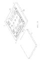
- FIG. 1 illustrates a SIM card connector 1 in prior art, which is disclosed in a Singaporean patent application No. SG201106636-2.
- the SIM card connector 1 includes a terminal seat 10 and a metal shell 13 .
- the metal shell 13 and the terminal seat 10 are assembled together to form a space receiving the SIM card.
- the terminal seat 10 includes a housing 11 and a plurality of terminals 12 .
- the housing 11 is generally made from plastic, the plurality of terminals 12 are fixed to the housing 11 in an insert molding manner.
- the metal shell 13 has a plurality of soldering points 131 , and each terminal 12 has a soldering portion 121 .
- soldering point 131 and the soldering portion 121 are soldered on a corresponding soldering pad.
- the terminal seat 10 adopts a unitary design, and therefore, the terminal seat 10 has considerable length and width. Long and wide terminal seat 10 is easy to warp, so that it is difficult to ensure that the soldering points 131 of the metal shell 13 and the soldering portions 121 of the terminals 12 of the SIM card connector 1 are coplanar after the SIM card connector 1 is assembled.
- a structure of the terminal seat 10 would change generally after reflow is performed, which would worsen situations of warping of the terminal seat 10 and non-coplanarity of the soldering points 131 of the metal shell 13 and the soldering portions 121 of the terminals 12 .
- An embodiment of the present application provides an electrical connector, which includes a metal shell and two terminal seats, wherein the two terminal seats and the metal shell together define a mating slot.
- Each terminal seat includes a first end portion and a second end portion which are opposite, a housing, a metal frame and a plurality of terminals.
- the metal frame may be embedded in and fixed to the housing.
- the metal frame includes a bottom plate and two side plates. Each side plate includes a pivoting portion, each terminal seat is pivoted to the metal shell via the pivoting portions.
- the pivoting portion is positioned between the first end portion and the second end portion, and a distance from the pivoting portion to the first end portion is longer than a distance from the pivoting portion to the second end portion.
- the plurality of terminals are embedded in and fixed to the housing. Each terminal includes a contact portion and a soldering portion, the contact portion extends into the mating slot, and the soldering portion is positioned at the first end portion.
- the depicted electrical connector has two terminal seats, therefore the terminal seats can be small and less likely to warp.
- the terminal seats are pivoted to the metal shell, and therefore, the soldering portions of the terminals can be adjusted relative to the metal shell.
- FIG. 1 shows a SIM card connector in prior art
- FIG. 2 is a view of an embodiment of an electrical connector and an electronic card provided on a circuit board
- FIG. 3 is an exploded view of the electrical connector depicted in FIG. 2 ;
- FIG. 4 is another exploded view of the electrical connector depicted in FIG. 2 ;
- FIG. 5 is a perspective exploded view of an embodiment of terminals, an housing and a metal frame
- FIG. 6 is another perspective view of the embodiment depicted in FIG. 5 ;
- FIG. 7 is an elevated side view illustrating that the terminal seats of an electrical connector in a first position
- FIG. 8 is an elevated side view illustrating the terminal seats of the electrical connector of FIG. 7 in a second position
- FIG. 9 is a bottom view of an embodiment of an electrical connector
- FIG. 11 is a bottom view of an embodiment of a terminal seat
- FIG. 12 is a top view of an embodiment of a terminal seat
- FIG. 13 is a cross-sectional view taken along a line 13 - 13 of FIG. 11 ;
- FIG. 14 is a top view of an embodiment of a peripheral edge region.
- FIG. 2 is a view of an electrical connector 2 provided on a circuit board 3 and an electronic card 4 in an embodiment of the present application.
- FIG. 3 is an exploded view of the electrical connector 2 of FIG. 2 .
- FIG. 4 is another exploded view of the electrical connector 2 of FIG. 2 .
- an electrical connector 2 may be mounted on the circuit board 3 extending in a horizontal direction to receive an electronic card 4 (for example a SIM card).
- an electronic card 4 for example a SIM card
- the present application takes a SIM card connector and the SIM card as an exemplary embodiment, the present application is not limited to them. The concept of the present application can be also applied to other electrical connectors.
- the electrical connector 2 includes a metal shell 23 and a plurality of terminal seats 20 .
- the metal shell 23 is positioned on the plurality of terminal seats 20 , and the plurality of terminal seats 20 are connected to the metal shell 23 in a pivoting manner.
- the metal shell 23 and the plurality of terminal seats 20 together define a mating slot 5 , and the electronic card 4 can be inserted into the mating slot 5 from a mating direction 8 .
- the metal shell 23 includes a top plate 231 and two side plates 232 .
- the two side plates 232 are respectively positioned at two opposite sides of the top plate 231 , therefore, two side plates 232 and the top plate 231 together form a receiving space which can receive the terminal seats 20 .
- the metal shell 23 may comprise a plurality of soldering pieces 233 , the plurality of soldering pieces 233 may be provided respectively in the two side plates 232 .
- the soldering piece 233 may be bent and positioned below the receiving space. With the soldering pieces 233 , the metal shell 23 may be soldered on the circuit board 3 .
- each terminal seat 20 includes a first end portion 28 and a second end portion 29 , the first end portion 28 and the second end portion 29 are opposite.
- Each terminal seat 20 may comprise a housing 21 , a plurality of terminals 22 , and a metal frame 24 .
- the housing 21 may be formed of a resin
- the metal frame 24 and the plurality of terminals 22 can be fixed to the housing 21 by an insert molding process so as to form the terminal seat 20 , wherein the plurality of terminals 22 may be arranged in a transverse direction 7 , and the transverse direction 7 may be perpendicular to the mating direction 8 .
- the metal frame 24 may be positioned at the second end portion 29 of the terminal seat 20 .
- the terminal 22 includes a flat plate portion 220 , a soldering portion 222 , a resilient arm 224 , and a contact portion 225 .
- the flat plate portion 220 includes a base 221 and two wing portions 223 .
- the resilient arm 224 obliquely extends upwardly from a first end 2211 of the base 221 .
- the contact portion 225 is formed at a distal end of the resilient arm 224 , and may extend into the mating slot 5 .
- the base 221 has a second end 2212 , the second end 2212 may be opposite to the first end 2211 , the soldering portion 222 extends from the second end 2212 of the base 221 and positioned at the first end portion 28 .
- a length of the terminal seat 20 may be shortened in the mating direction 8 of the electronic card 4 , so as to avoid obvious warping generated in the length direction and influencing coplanarity of the soldering pieces 233 of the metal shell 23 and the soldering portions 222 of the terminals 22 .
- a mold required to manufacture the shorter terminal seat 20 is small, so as to reduce manufacturing cost.
- the plurality of terminal seats 20 may be identical, so that the plurality of terminal seats 20 of the electrical connector 2 may be produced with the same mold, so as to reduce production cost.
- the metal frame 24 includes a bottom plate 241 and two side plates 242 .
- the two side plates 242 are provided at two opposite sides of the bottom plate 241 to define two sides of the mating slot 5 .
- Each side plate 242 includes a pivoting portion 2421 , wherein each terminal seat 20 is pivoted to the metal shell 23 via the pivoting portions 2421 of the side plates 242 .
- the pivoting portion 2421 of each side plate 242 may be positioned between the first end portion 28 and the second end portion 29 of the corresponding terminal seat 20 .
- a distance L 1 from the pivoting portion 2421 of each side plate 242 to the first end portion 28 of the terminal seat 20 is longer than a distance L 2 from the pivoting portion 2421 to the second end portion 29 .
- the pivoting portion 2421 may be a pivoting shaft transversely protruding outwardly from the corresponding side plate 242 , and the side plate 232 of the metal shell 23 is provided with a corresponding pivoting hole 234 capable of allowing the pivoting shaft to rotate.
- the terminal seat 20 may pivot relative to the metal shell 23 to adjust the soldering portions 222 of the terminals 22 in an up-down direction relative to the soldering piece 233 of the metal shell 23 , so as to allow compensation for coplanarity deviation between the soldering portions 222 of the terminals 22 and the soldering pieces 233 of the metal shell 23 .
- the side plate 242 of the metal frame 24 may comprise a first stopping portion 2422 , the first stopping portion 2422 may be close to the second end portion 29 of the terminal seat 20 , and the first stopping portion 2422 may stop at the metal shell 23 , as shown in FIG. 7 and FIG. 10 .
- the side plate 242 of the metal frame 24 may further comprise a second stopping portion 2423 , the second stopping portion 2423 may be close to the first end portion 28 of the terminal seat 20 , and the second stopping portion 2423 may stop at the metal shell 23 , as shown in FIG. 8 .
- each terminal seat 20 may pivot between a first position ( FIG. 7 ) and a second position ( FIG. 8 ) relative to the metal shell 23 .
- a soldering face 2221 of the soldering portion 222 of the terminal 22 would be lower than a soldering face 2331 of the soldering piece 233 of the metal shell 23 .
- the soldering face 2221 of the soldering portion 222 of the terminal 22 would be flush with the soldering face 2331 of the soldering piece 233 of the metal shell 23 .
- the soldering portions 222 of the terminals 22 would droop downwardly until the first stopping portion 2422 of the side plate 242 stops at the metal shell 23 .
- the soldering portions 222 of the terminals 22 would first contact respective soldering pads on the circuit board 3
- the soldering portions 222 of the terminals 22 would continuously contact the respective soldering pads on the circuit board 3
- the soldering pieces 233 of the metal shell 23 contact the respective soldering pads on the circuit board 3 .
- the housing 21 includes a bottom face 211
- the terminal 22 includes a flat plate portion 220
- the flat plate portion 220 includes a bottom face 2201 , wherein the bottom face 2201 of the flat plate portion 220 is flush with the bottom face 211 of the housing 21 ( FIG. 13 ).
- the hollow portion 226 includes the opening 2262 at the edge 2231 of the wing portion 223 and the middle portion 2261 formed by extending into the wing portion 223 , wherein the width w of the opening 2262 is smaller than the width W of the middle portion 2261 .
- the hollow portion 226 of the wing portion 223 is similar to a mortise of puzzle pieces.
- the hollow portion 226 of the wing portion 223 includes a dovetail shape. That the wing portion 223 is provided with the hollow portion 226 may remedy a defect that the flat plate portion 220 is difficult to hold, and firmly hold the terminals 22 with the housing 21 so as to be not easily separated in the horizontal direction.
- each wing portion 223 has a peripheral edge region 2232 , the peripheral edge region 2232 surrounds the hollow portion 226 along the edge 2263 of the hollow portion 226 , wherein the hollow portion 226 of each wing portion 223 and the peripheral edge region 2232 of each wing portion 223 are embedded in housing 21 .
- a part of the housing 21 fills each hollow portion 226 and extends until to cover the peripheral edge region 2232 on the upper surface 2234 of each wing portion 223 , in this way, a partial surface of each wing portion 223 may be exposed, which may reduce the housing 21 covering the terminal 22 , so as to avoid warping of the terminal seat 20 .
- a peripheral edge region 2232 ′ may extend along the edge 2263 of the hollow portion 226 with an equal width, or expand outwardly from the edge 2263 of the hollow portion 226 with an equal distance (as shown with arrows in FIG. 14 ).
- the peripheral edge region 2232 may be considered as a region expanding outwardly from the edge 2263 of the hollow portion 226 on the wing portion 223 .
- an area of the peripheral edge region 2232 does not exceed an exposed area of the wing portion 223 after the insert molding process.
- the wing portion 223 can be two areas partitioned by a central line, wherein the peripheral edge region 2232 is positioned in one area, and more than half segments of the peripheral edge region 2232 do not expand to exceed the central line.
- the central line 100 may be determined by the following method.
- a plurality of first points P 1 are determined on the edge 2263 of the hollow portion 226
- a plurality of corresponding second points P 2 are determined on edges ( 101 and 102 ) and the side edge 2213 of the wing portion 223 .
- the plurality of first points P 1 and the plurality of second points P 2 are arranged in the same manner. In other words, if the plurality of first points P 1 equally divide the edge 2263 of the hollow portion 226 , the plurality of second points P 2 also equally divide the edges ( 101 and 102 ) and the side edge 2213 . Then, a midpoint of a connection line between the corresponding first point P 1 and the second point P 2 is determined. Finally, the central line 100 connecting a plurality of midpoints is determined.
- each wing portion 223 includes at least one clamping portion 2233 , the at least one clamping portion 2233 defines an opening 2262 , wherein the at least one clamping portion 2233 is embedded in the housing 21 .
- each wing portion 223 includes two clamping portions 2233 , wherein the two clamping portions 2233 are embedded in the housing 21 .
- the metal frame 24 can be fixed to the housing 21 by the insert molding manner, thereby strengthening the housing 21 .
- the metal frame 24 includes a bottom plate 241 and two side plates 242 .
- the bottom plate 241 includes two upright frames 2413 and a transverse frame 2411 , wherein the two upright frames 2413 are respectively connected to the two side plates 242 , and the transverse frame 2411 is connected to the two upright frames 2413 .
- the bottom plate 241 may not comprise the two upright frames 2413 , wherein the transverse frame 2411 is connected to the two side plates 242 .
- the transverse frame 2411 may be provided with a plurality of hollow portions 2412 , each hollow portion 2412 includes an middle portion 24121 .
- Each second hollow portion 2412 extends toward an edge 24111 of the transverse frame 2411 and forms a second opening 24112 at the edge 24111 of the transverse frame 2411 , wherein a width of the second opening 24112 is smaller than a width of the middle portion 24121 of the second hollow portion 2412 in a direction parallel to a width direction of the second opening 24112 .
- each opening 24112 is defined by at least one clamping portion 24114 , wherein the at least one clamping portion 24114 is embedded in the housing 21 .
- each upright frame 2413 includes a plurality of hollow portions 2414 .
- Each hollow portion 2414 includes an middle portion 24141 , each hollow portion 2414 extends toward an edge 24131 of the corresponding upright frame 2413 and forms an opening 24142 at the edge 24131 , a width of the opening 24142 is smaller than a width of the middle portion 24141 in a direction parallel to a width direction of the opening 24142 .
- each opening 24142 is defined by at least one clamping portion 24132 , wherein the at least one clamping portion 24132 is embedded in the housing 21 .
- the transverse frame 2411 includes a bottom face 24113 .
- the bottom face 24113 may be flush with the bottom face 211 of the housing 21 .
- a part of the housing 21 fills each hollow portion 2412 and extends to cover a partial upper surface of the two upright frames 2413 and the transverse frame 2411 .
- the above described part of the housing 21 may further fill each hollow portion 2414 of the upright frame 2413 .
- each hollow portion 2412 and a peripheral edge region surrounding each hollow portion 2412 on the upper surface of the transverse frame 2411 are embedded in the housing 21 .
- the electrical connector in the embodiments of the present application includes the plurality of terminal seats, wherein the terminal seat includes the housing and the terminals fixed to the housing.
- the design of the plurality of terminal seats is adopted so as to shorten the lengths of the terminal seats, so as to avoid a problem of poor coplanarity of the terminal soldering portions caused by warping of the housing which is caused by using long housing.
- the terminal seats are pivoted to the metal shell, in this way, a relative position between the soldering pieces of the metal shell and the soldering portions of the terminals can be adjusted in the up-down direction, so as to ensure that the soldering pieces of the metal shell and the soldering portions of the terminals can be properly soldered on the circuit board.
- the terminal includes the flat plate portion, and the flat plate portion includes the wing portion fixed to the housing and having the hollow portion.
- the part of the housing fills each hollow portion and extends to cover the partial upper surface of each wing portion, thereby avoiding warping of the terminal seat caused by non-uniform distribution of the housing material covered on upper and lower surfaces of the wing portions.
Landscapes
- Coupling Device And Connection With Printed Circuit (AREA)
Abstract
Description
Claims (12)
Applications Claiming Priority (6)
| Application Number | Priority Date | Filing Date | Title |
|---|---|---|---|
| CN 201220218672 CN202662852U (en) | 2012-05-15 | 2012-05-15 | Electrical connector |
| CN201210150832 | 2012-05-15 | ||
| CN201220218672.3 | 2012-05-15 | ||
| CN201210150832.2 | 2012-05-15 | ||
| CN201210150832.2A CN103427211B (en) | 2012-05-15 | 2012-05-15 | Electrical connector |
| CN201220218672U | 2012-05-15 |
Publications (2)
| Publication Number | Publication Date |
|---|---|
| US20130323980A1 US20130323980A1 (en) | 2013-12-05 |
| US8979593B2 true US8979593B2 (en) | 2015-03-17 |
Family
ID=49670768
Family Applications (1)
| Application Number | Title | Priority Date | Filing Date |
|---|---|---|---|
| US13/894,882 Active 2033-09-13 US8979593B2 (en) | 2012-05-15 | 2013-05-15 | Low profile electrical connector |
Country Status (1)
| Country | Link |
|---|---|
| US (1) | US8979593B2 (en) |
Families Citing this family (1)
| Publication number | Priority date | Publication date | Assignee | Title |
|---|---|---|---|---|
| JP7368069B2 (en) * | 2019-09-02 | 2023-10-24 | 日本航空電子工業株式会社 | connector |
Citations (11)
| Publication number | Priority date | Publication date | Assignee | Title |
|---|---|---|---|---|
| US6083018A (en) * | 1999-02-05 | 2000-07-04 | Hon Hai Precision Ind. Co., Ltd. | Memory card connector |
| US6146163A (en) * | 1998-06-02 | 2000-11-14 | Hon Hai Precision Ind. Co., Ltd. | Ejection mechanism for electrical card connector |
| US20050159037A1 (en) * | 2004-01-20 | 2005-07-21 | Chia-Sheng Su | Electronic card connector |
| US7537486B2 (en) * | 2007-06-08 | 2009-05-26 | Mea Technologies Pte. Ltd. | Card connector |
| US7833063B2 (en) * | 2005-09-22 | 2010-11-16 | Molex Incorporated | Card connector |
| US20100291785A1 (en) * | 2009-05-12 | 2010-11-18 | Hon Hai Precision Industry Co., Ltd. | Elelctrical connector with a cover rotatably assembled on a housing |
| US20110008985A1 (en) * | 2007-10-26 | 2011-01-13 | Molex Incorporated | Card connector for receiving multiple cards |
| US7896670B1 (en) | 2010-04-30 | 2011-03-01 | Cheng Uei Precision Industry Co., Ltd. | Card connector |
| US20110151721A1 (en) * | 2009-12-23 | 2011-06-23 | Hon Hai Precision Industry Co., Ltd. | Electrical card connector |
| CN202906112U (en) | 2011-09-15 | 2013-04-24 | 美国莫列斯股份有限公司 | Electronic card connector |
| US20130157481A1 (en) | 2011-12-19 | 2013-06-20 | Molex Incorporated | Electrical connector assembly |
-
2013
- 2013-05-15 US US13/894,882 patent/US8979593B2/en active Active
Patent Citations (13)
| Publication number | Priority date | Publication date | Assignee | Title |
|---|---|---|---|---|
| US6146163A (en) * | 1998-06-02 | 2000-11-14 | Hon Hai Precision Ind. Co., Ltd. | Ejection mechanism for electrical card connector |
| US6083018A (en) * | 1999-02-05 | 2000-07-04 | Hon Hai Precision Ind. Co., Ltd. | Memory card connector |
| US20050159037A1 (en) * | 2004-01-20 | 2005-07-21 | Chia-Sheng Su | Electronic card connector |
| US7833063B2 (en) * | 2005-09-22 | 2010-11-16 | Molex Incorporated | Card connector |
| US7537486B2 (en) * | 2007-06-08 | 2009-05-26 | Mea Technologies Pte. Ltd. | Card connector |
| US20110008985A1 (en) * | 2007-10-26 | 2011-01-13 | Molex Incorporated | Card connector for receiving multiple cards |
| US7976327B2 (en) * | 2007-10-26 | 2011-07-12 | Molex Incorporated | Card connector for receiving multiple cards |
| US20100291785A1 (en) * | 2009-05-12 | 2010-11-18 | Hon Hai Precision Industry Co., Ltd. | Elelctrical connector with a cover rotatably assembled on a housing |
| US20110151721A1 (en) * | 2009-12-23 | 2011-06-23 | Hon Hai Precision Industry Co., Ltd. | Electrical card connector |
| US8011965B2 (en) * | 2009-12-23 | 2011-09-06 | Hon Hai Precision Ind. Co., Ltd. | Electrical card connector |
| US7896670B1 (en) | 2010-04-30 | 2011-03-01 | Cheng Uei Precision Industry Co., Ltd. | Card connector |
| CN202906112U (en) | 2011-09-15 | 2013-04-24 | 美国莫列斯股份有限公司 | Electronic card connector |
| US20130157481A1 (en) | 2011-12-19 | 2013-06-20 | Molex Incorporated | Electrical connector assembly |
Also Published As
| Publication number | Publication date |
|---|---|
| US20130323980A1 (en) | 2013-12-05 |
Similar Documents
| Publication | Publication Date | Title |
|---|---|---|
| US6994566B2 (en) | Circuit board mounted electrical connector | |
| US9318837B2 (en) | Electrical connector | |
| US20160164206A1 (en) | Printed Circuit Board Centering Beam | |
| KR101309404B1 (en) | A connecting apparatus for a terminal | |
| TWI716661B (en) | Card edge connector | |
| US8052449B2 (en) | Card edge connector with floating pad thereon | |
| US8794985B2 (en) | Card Edge Connector | |
| US20140302719A1 (en) | Card edge connector | |
| CN1983728A (en) | Electronic-card connector | |
| US20100317232A1 (en) | Low profile socket connector and method for making the same | |
| US8979593B2 (en) | Low profile electrical connector | |
| JP3703741B2 (en) | IC socket | |
| US9004934B2 (en) | Card edge connector | |
| US20130084717A1 (en) | Board to board connectors and assembly thereof with contact-mounting wall having variable thickness | |
| US9130321B2 (en) | Electrical connector having contact for either BGA or LGA package | |
| TWI332294B (en) | ||
| US20160072208A1 (en) | Electrical connector | |
| SG176336A1 (en) | Sim card connector and sim card connector assembly including the same | |
| JP7073054B2 (en) | Receptacle connector and manufacturing method of receptacle connector | |
| WO2011150307A2 (en) | Sim card connector | |
| US9590330B2 (en) | Electrical connector | |
| KR101580140B1 (en) | SIM Card Connection Terminal | |
| TWM441239U (en) | Electrical connector | |
| TWM484225U (en) | Electrical connector | |
| US7753692B2 (en) | Socket connector having improved arrangement ensuring reliable and robust alignment between conductive contacts |
Legal Events
| Date | Code | Title | Description |
|---|---|---|---|
| AS | Assignment |
Owner name: MOLEX INCORPORATED, ILLINOIS Free format text: ASSIGNMENT OF ASSIGNORS INTEREST;ASSIGNORS:LIM, KIAN-HENG;TAN, HAN-GUAN;REEL/FRAME:031035/0131 Effective date: 20130704 |
|
| STCF | Information on status: patent grant |
Free format text: PATENTED CASE |
|
| MAFP | Maintenance fee payment |
Free format text: PAYMENT OF MAINTENANCE FEE, 4TH YEAR, LARGE ENTITY (ORIGINAL EVENT CODE: M1551); ENTITY STATUS OF PATENT OWNER: LARGE ENTITY Year of fee payment: 4 |
|
| MAFP | Maintenance fee payment |
Free format text: PAYMENT OF MAINTENANCE FEE, 8TH YEAR, LARGE ENTITY (ORIGINAL EVENT CODE: M1552); ENTITY STATUS OF PATENT OWNER: LARGE ENTITY Year of fee payment: 8 |
|
| AS | Assignment |
Owner name: MOLEX, LLC, ILLINOIS Free format text: CHANGE OF NAME;ASSIGNOR:MOLEX INCORPORATED;REEL/FRAME:062820/0197 Effective date: 20150819 |