US8963639B2 - Frequency compensation techniques for low-power and small-area multistage amplifiers - Google Patents
Frequency compensation techniques for low-power and small-area multistage amplifiers Download PDFInfo
- Publication number
- US8963639B2 US8963639B2 US13/770,020 US201313770020A US8963639B2 US 8963639 B2 US8963639 B2 US 8963639B2 US 201313770020 A US201313770020 A US 201313770020A US 8963639 B2 US8963639 B2 US 8963639B2
- Authority
- US
- United States
- Prior art keywords
- stage
- gain
- output
- amplifier
- transistor
- Prior art date
- Legal status (The legal status is an assumption and is not a legal conclusion. Google has not performed a legal analysis and makes no representation as to the accuracy of the status listed.)
- Active, expires
Links
Images


Classifications
-
- H—ELECTRICITY
- H03—ELECTRONIC CIRCUITRY
- H03F—AMPLIFIERS
- H03F3/00—Amplifiers with only discharge tubes or only semiconductor devices as amplifying elements
- H03F3/45—Differential amplifiers
- H03F3/45071—Differential amplifiers with semiconductor devices only
- H03F3/45076—Differential amplifiers with semiconductor devices only characterised by the way of implementation of the active amplifying circuit in the differential amplifier
- H03F3/45179—Differential amplifiers with semiconductor devices only characterised by the way of implementation of the active amplifying circuit in the differential amplifier using MOSFET transistors as the active amplifying circuit
- H03F3/45183—Long tailed pairs
- H03F3/45192—Folded cascode stages
-
- H—ELECTRICITY
- H03—ELECTRONIC CIRCUITRY
- H03F—AMPLIFIERS
- H03F2200/00—Indexing scheme relating to amplifiers
- H03F2200/408—Indexing scheme relating to amplifiers the output amplifying stage of an amplifier comprising three power stages
-
- H—ELECTRICITY
- H03—ELECTRONIC CIRCUITRY
- H03F—AMPLIFIERS
- H03F2203/00—Indexing scheme relating to amplifiers with only discharge tubes or only semiconductor devices as amplifying elements covered by H03F3/00
- H03F2203/45—Indexing scheme relating to differential amplifiers
- H03F2203/45631—Indexing scheme relating to differential amplifiers the LC comprising one or more capacitors, e.g. coupling capacitors
-
- H—ELECTRICITY
- H03—ELECTRONIC CIRCUITRY
- H03F—AMPLIFIERS
- H03F2203/00—Indexing scheme relating to amplifiers with only discharge tubes or only semiconductor devices as amplifying elements covered by H03F3/00
- H03F2203/45—Indexing scheme relating to differential amplifiers
- H03F2203/45674—Indexing scheme relating to differential amplifiers the LC comprising one current mirror
Definitions
- the present invention is related to an amplifier, and, in particular, to an amplifier with small power and area.
- High-color-depth LCD drivers demand an extensive number of amplifiers to buffer the Gamma-corrected reference voltages, which have to be stabilized by nF-range capacitors to handle the glitch energy during the digital-to-analog conversion.
- the present invention is directed to a three stage amplifier.
- the three stage amplifier includes first, second and third gain stages wherein said first stage receives an amplifier input signal and said third gain stage outputs an amplifier output signal.
- the three stage amplifier includes a feedback loop having a current buffer and a compensation capacitance provided from the output of said third gain stage to the output of the first gain stage.
- An active left half plane zero stage is embedded in said feedback loop for cancelling a parasitic pole of said feedback loop.
- the active left half plane zero stage includes two gain stages, and the feedback loop includes a resistance and a second compensation capacitance.
- an active left half plane zero stage is embedded inside the third stage.
- said three gain stages in are negative gain stages.
- the amplifier comprises a feedforward transconductance stage extending from the output of first gain stage to the output of said three stage amplifier.
- an active left half plane zero stage is embedded inside the output stage.
- a feedforward transconductance stage is extending from the output of said first gain stage to the output of said third gain stage.
- an active left half plane zero stage embedded in the second stage for cancelling a parasitic pole of said feedback loop is provided.
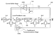
- FIG. 1 a shows a schematic circuit diagram illustrating the structure of a three stage amplifier 100 according to an embodiment of the invention.
- FIG. 1 b shows a schematic circuit diagram of the active Left half plane zero stage 122 according to an embodiment of the invention.
- FIG. 3 b shows an exemplary schematic view of the current buffer circuit 114 according to an embodiment of the invention.
- FIG. 4 a shows an output noise density of the amplifier 200 according to an embodiment of the invention.
- FIG. 4 b shows power-supply rejection ratio (PSRR) of the amplifier 200 according to an embodiment of the invention.
- FIG. 4 c shows a gain response in unity-gain feedback of the amplifier 200 according to an embodiment of the invention.
- FIG. 5 c shows the simulated gain and phase margins of the amplifier 200 according to an embodiment of the invention.
- FIG. 1 a shows a schematic circuit diagram illustrating the structure of a three stage amplifier 100 according to an embodiment of the invention.
- the three stage amplifier 100 comprises three main gain stages Av 1 , Av 2 , and Av 3 .
- the three stage amplifier 100 further comprises a feedforward transconductance stage Avfw, an active left half plane zero stage 122 , a current buffer stage 114 and a Miller compensation capacitance Cm.
- parasitic capacitances Cp 1 , Cp 2 , and parasitic transconductance resistances go 1 , go 2 , goL.
- the gain stage Av 1 receives an amplifier input signal Vi and generates a signal V 1 depending on a negative transconductance gain ⁇ Gm 1 .
- the gain stage Av 2 is coupled to the gain stage Av 1 and receives the signal V 1 and generates a signal V 2 depending on a negative transconductance gain ⁇ Gm 2 .
- the gain stage Av 3 is coupled to the gain stage Av 2 and generates an amplifier output signal Vo depending on a negative transconductance gain ⁇ GmL.
- the parasitic capacitance Cp 1 and the parasitic transconductance resistance go 1 parasitize between an output of the gain stage Av 1 and ground respectively; the parasitic capacitance Cp 2 and the parasitic transconductance resistance go 2 parasitize between an output of the gain stage Av 2 and ground respectively; and the parasitic transconductance resistance goL parasitizes between an output of the gain stage Av 3 and ground, wherein a load capacitance CL is coupled between the output of the gain stage Av 3 and ground too.
- a local feedback loop goes from the output of the gain stage Av 3 to the input of the gain stage Av 3 with the Miller compensation capacitance Cm coupled between the gain stages Av 2 and Av 3 .
- the active left half plane zero stage 122 can be coupled anywhere on the path of the feedback loop for contributing frequency compensation to the amplifier output signal Vo, that is, the active left half plane zero stage 122 is embedded in the feedback loop for cancelling a parasitic pole of the feedback loop.
- the active left half plane zero stage 122 is coupled on the path where the gain stage Av 3 is coupled to the gain stage Av 2 , and sending a signal V 3 to the gain stage Av 3 by compensating the signal V 2 .
- FIG. 1 b shows a schematic circuit diagram of the active Left half plane zero stage 122 according to an embodiment of the invention.
- the active left half plane zero stage 122 further includes gain stages Avb 1 , Avb 2 having negative transconductance gain ⁇ Gmb 1 and ⁇ Gmb 2 respectively, a capacitance Cz and a resistance Rz.
- a parasitic capacitance Cpb and a parasitic transconductance resistance gop parasitize between an output of the gain stage Avb 1 and ground respectively.
- the capacitance Cz is coupled between an input of the gain stage Avb 1 and ground.
- the resistance Rz is coupled between the input and the output of the gain stage Avb 1 .
- the gain stage Avb 2 is coupled to the gain stage Avb 1 and receives the signal V 2 .
- the current buffer stage 114 is also coupled on the path of the local feedback loop for avoiding the bandwidth reduction originated from the RC network in the three stage amplifier 100 .
- the current buffer stage 114 includes a gain stage Avfb with a transconductance gain Gma and a parasitic transconductance resistance gma.
- An input of the gain stage Avfb is coupled to the Miller compensation capacitance Cm and an output of the gain stage Avfb is coupled to the gain stage Av 2 .
- the parasitic transconductance resistance gma exists between the input of the gain stage Avfb and ground.
- the amplifier 100 uses the feedforward transconductance stage Avfw to make gain compensation for the amplifier output signal Vo. Further, the feedforward transconductance stage Avfw has a negative transconductance gain gin ⁇ Gmf and is coupled between the outputs of the gain stages Av 1 and Av 3 .
- the LFL (local feedback loop) transfer function of the three stage amplifier 100 can be obtained
- a Proposed ⁇ ( s ) ⁇ A DC ⁇ ( 1 + s A f ⁇ P 1 + s 2 A f ⁇ P 1 ⁇ P 2 ) ⁇ ( 1 + s P 3 ) ( 1 + 5 ⁇ pd ) ⁇ ( 1 + s ⁇ ⁇ , Proposed + s 2 ⁇ ⁇ , Proposed ⁇ P 1 + s 3 ⁇ ⁇ , Proposed ⁇ P 1 ⁇ P 2 + s 4 ⁇ ⁇ , Proposed ⁇ P 1 ⁇ P 2 ⁇ P 3 ) ⁇ A DC ( 1 + s ⁇ pd ) ⁇ ( 1 + 2 ⁇ ⁇ ⁇ ( s ⁇ n ) + ( s ⁇ n ) 2 ) A DC ( 1 + s ⁇ pd ) ⁇ ( 1 + s ⁇ ⁇ , Proposed + s 2 K ⁇ ⁇ p , Proposed 2 ) ( 2 ) where A f is (G m
- the GBW is (G m1 /C m ).
- the damping factor ⁇ and natural frequency ⁇ n of the second-order polynomial in the denominator of (2) can be characterized by the LFL parameters ⁇ ⁇ ,Proposed and K, which are manifested as,
- the exact relationship among GBW, ⁇ , and ⁇ n can be determined by a proper set of coefficients for the denominator of the 3 rd -order closed-loop transfer function, which is obtained by configuring the amplifier in unity-gain feedback (e.g., Butterworth coefficients).
- a more design-oriented approach is to link up the LFL parameters ( ⁇ ⁇ ,Proposed and PM LFL ) to those of the amplifier (GBW and PM) as given by,
- G m2 and G mL The optimization of G m2 and G mL involves the power tradeoff between the 2 nd and 3 rd stages, and can be obtained by the estimated C p1 and C p2 . Finally, G mf should match G mL for realizing a symmetric output stage.
- the SR (slew rate) of the proposed amplifier 100 is mainly constrained by those of the first and final stages since the lumped parasitic capacitance Cp 2 is much smaller than Cm and CL.
- the SR is not limited by the push-pull output stage if CL ⁇ 5 nF (in the designed amplifier) as given by,
- the SR of the proposed amplifier 100 can be expressed as,
- the simplified 3rd-order transfer function (2) can help to analyze the linear settling behavior, which can be fully determined by the three open-loop parameters: GBW, ⁇ , and ⁇ n.
- GM gain margin
- the amplifier 200 includes a current transferring amplifying unit 110 , a frequency compensation unit 120 , an output driving unit 130 , and a Miller compensation capacitance Cm (which is corresponding to Cm of FIG. 1 a ).
- the current transferring amplifying unit 110 includes a current buffer circuit 114 (which is corresponding to the current buffer stage 114 of FIG. 1 a ) embedded inside the current transferring amplifying unit 110 .
- the frequency compensation unit 120 includes an active left half plane zero circuit 122 (which is corresponding to active left half plane zero stage 122 of FIG. 1 a ) embedded thereof.
- the current transferring amplifying unit 110 could be regarded as a first gain stage.
- the current transferring amplifying unit 110 receives an input signals Vin, Vip (which are corresponding to the signal V 1 of FIG. 1 a ) and generates a first stage output signal Sp 1 (which is corresponding to the signal V 2 of FIG. 1 a ) with a gain Gm 1 (which is corresponding to ⁇ Gm 1 of FIG. 1 a ).
- the current transferring amplifying unit 110 amplifies the input signals Vin, Vip to generate the first stage output signal Sp 1 with the gain Gm 1 at the output thereof.
- the current buffer circuit 114 contributes at least a part of gain component Gma (which is corresponding to Gma of FIG. 1 a ) to the gain Gm 1 .
- the output driving unit 130 is coupled to the frequency compensation unit 120 and receives the second stage output signal Sp 2 .
- the output driving unit 130 receives the second stage output signal Sp 2 to drive the third stage output signal Vo (which is also an output signal of the amplifier 200 ) at an output of the amplifier 200 according to the second stage output signal Sp 2 .
- the Miller compensation capacitance Cm is coupled between the output of the amplifier 200 and an input of the current buffer circuit 114 .
- the current transferring amplifying unit 110 further includes a differential input port 112 and the differential input port 112 receives a pair of input differential signals Vin and Vip.
- the differential input port 112 transports transporting signals St 1 and St 2 to the current buffer circuit 114 according to the input signals Vin and Vip.
- the input port 112 includes a transistor M 1 (e.g. a P-type transistor), a transistor M 2 (e.g. a P-type transistor), and a transistor Mb 1 (e.g. a P-type transistor).
- the transistors M 1 , M 2 , and Mb 1 include e.g. a source, a drain and a gate.
- the gate of the transistor M 1 receives the input signal Vin and the transporting signal St 1 is generated at the drain of the transistor M 1 .
- the gate of the transistor M 2 receives the input signal Vip and the transporting signal St 2 is generated at the drain of the transistor M 2 .
- the gate of the transistor Mb 1 receives a bias voltage Vb 1
- the source of the transistor Mb 1 receives a power voltage VDD
- the drain of the transistor Mb 1 is coupled to both the sources of the transistors M 1 and M 2 .
- the bias voltage Vb 1 could be provided properly to the transistor Mb 1 so as to drive a suitable current I 1 for the differential input port 112 .
- the current buffer circuit 114 includes a transistor M 3 (e.g. an N-type transistor), a transistor M 4 (e.g. an N-type transistor), a transistor M 7 (e.g. an N-type transistor) and a transistor M 8 (e.g. an N-type transistor).
- the transistors M 3 , M 4 , M 7 and M 8 include e.g. a source, a drain and a gate.
- the source of the transistor M 3 receives a ground voltage VSS
- the gate of the transistor M 3 receives a bias voltage Vb 2
- the drain of the transistor M 3 receives the transporting signal St 1 .
- the source of the transistor M 4 receives a ground voltage VSS, the drain of the transistor M 4 receives the bias voltage Vb 2 , and the drain of the transistor receives the transporting signal St 2 .
- the source of the transistor M 7 receives the transporting signal St 1 , the gate of the transistor M 7 receives a bias voltage Vba, and the drain of the transistor M 7 generates a current buffer signal Sc 1 .
- the source of the transistor M 8 receives the transporting signal St 2 , the gate of the transistor M 8 receives a bias voltage Vbb, and the drain of the transistor M 8 generates a current buffer signal Sc 2 .
- the current buffer signals Sc 1 and Sc 2 are generated and amplified with a gain GMA.
- the current transferring amplifying unit 110 further includes a cascode amplifying circuit 215 .
- the cascode amplifying circuit 215 also helps to amplify the differential current buffer signals Sc 1 and Sc 2 to generate the first stage output signal Sp 1 .
- the cascode amplifying circuit 215 includes a transistor M 9 (e.g. a P-type transistor) and a transistor M 10 (e.g. a P-type transistor).
- the transistors M 9 and M 10 have e.g. a source, a gate and a drain.
- the drain of the transistor M 9 receives the current buffer signal Sc 1 , the gate of the transistor M 9 is coupled to the drain of the transistor M 9 , and the source of the transistor M 9 receives a power voltage VDD.
- the drain of the transistor M 10 receives the current buffer signal Sc 2 , the gate of the transistor M 10 is coupled to the gate of the transistor M 9 , and the source of the transistor M 10 receives a power voltage VDD.
- the first stage output signal Sp 1 is generated at the drain of the transistor M 10 with a gain Gm 1 .
- a very large gain value for the gain Gma is desired to push a pole P 3 (which is corresponding to P 3 in the embodiment of FIGS. 1 a and 1 b ) to a high frequency.
- FIG. 3 a shows an exemplary schematic view of the current buffer circuit 114 according to an embodiment of the invention.
- the current buffer circuit 114 includes transistors M 3 , M 4 , M 7 and M 8 wherein the coupling relation among the transistors M 3 , M 4 , M 7 and M 8 is similar to the coupling relation of those transistors in the current buffer circuit 114 of FIG. 2 and will not repeat herein again.
- Both the gates of the transistors M 3 and M 4 receive a bias voltage Vb 2 and both the gates of the transistors M 7 and M 8 receive a bias voltage Vba.
- the gates of the transistors M 7 and M 8 are located at the same voltage level and thus a common gate design for the current buffer circuit 114 is achieved.
- the transistor M 8 is regarded as a simple current buffer. Therefore, the current buffer circuit 114 will draw considerable power to achieve the large gain Gma.
- the bias circuit 211 includes a current source 213 and a transistor M 5 (e.g. an N-type transistor).
- the transistor M 5 has e.g. a gate, a drain and a source.
- the source of the transistor M 5 receives a ground voltage VSS, and the gate of the transistor M 5 is coupled to the source of the transistor M 7 .
- the current source 213 is coupled between a power voltage VDD and the drain of the transistor M 5 .
- the bias circuit 212 includes a current source 214 and a transistor M 6 (e.g. an N-type transistor).
- the transistor M 6 has e.g. a gate, a drain and a source.
- the source of the transistor M 6 receives a ground voltage VSS, and the gate of the transistor M 6 is coupled to the source of the transistor M 8 .
- the current source 214 is coupled between a power voltage VDD and the drain of the transistor M 6 . Since the bias voltages Vba and Vbb are regulated according to the currents through the current source 213 and 214 respectively, a regulated design for the current buffer circuit 114 is achieved.
- the transistors M 6 and M 8 are formed as a regulated current buffer. Therefore, the gain GMA is boosted by a factor of (gm 6 *ro 6 +1), wherein gm 6 is a gain parameter of the transistor M 6 and ro 6 is the internal resistance of the transistor M 6 .
- the current buffer circuit 114 further includes bias circuits 211 and 212 wherein the bias circuits 211 and 212 are a regulated design as the embodiment of FIG. 3 b and the coupling relation among the bias circuits 211 and 212 and the current sources 213 and 214 is similar to the coupling relation among those in FIG. 3 b and thus will not repeat herein again.
- the current sources 213 and 214 can include resistances R 1 and R 2 respectively.
- the current transferring amplifying unit 110 further includes a transistor Mb 2 (e.g. a P-type transistor) coupled between a power voltage VDD and the bias circuits 211 and 212 .
- the transistor Mb 2 has e.g. a source, a drain and a gate.
- the source of the transistor Mb 2 receives a power voltage VDD
- the gate of the transistor Mb 2 receives the bias voltage Vb 1
- the drain of the transistor Mb 2 is coupled to terminals of the resistances R 1 and R 2 . Since the gate of the transistor Mb 2 receives the same bias voltage Vb 1 as the gate of transistor Mb 1 does, the current I 2 which is flowing into the resistances R 1 and R 2 can be regulated according to the current I 1 . Also, since the current I 2 flows into both the bias circuits 211 and 212 , a current I 3 flowing through the transistor M 7 and a current I 4 flowing through the transistor M 8 will be adjusted according to the current I 1 or I 2 .
- the transistors M 5 and M 6 and the resistances R 1 and R 2 are formed as a local feedback loop (LFL) which can provide a better controlled LFL gain (2*gm 5 *R 1 +1) with the moderately sized resistance R 1 , wherein gm 5 is the transconductance gain of the transistor M 5 .
- the output impedance of the transistor M 8 is also boosted by the LFL gain.
- the employed gain GMA in the embodiment of FIG. 2 balances the tradeoff between the gain Gma and bandwidth.
- the frequency compensation unit 120 could be regarded as a second gain stage.
- the frequency compensation unit 120 receives the first stage output signal Sp 1 and generates the second stage output signal Sp 2 with a gain Gm 2 (which is corresponding to ⁇ Gm 2 of FIG. 1 a ) with respect to the first stage output signal Sp 1 .
- the frequency compensation unit 120 in addition to the active left half plane zero circuit 122 , further comprises a transistor M 11 (e.g. a P-type transistor) and a transistor M 12 (e.g. a P-type transistor).
- the transistors M 11 and M 12 (which are corresponding to the gain stage Av 2 of FIG. 1 a ) have e.g.
- the source of the transistor M 11 receives the power voltage VDD
- the gate of the transistor M 11 receives the first stage output signal Sp 1
- the drain of the transistor M 11 generates a compensating signal Sa 1
- the source of the transistor M 12 receives a power voltage VDD and the gate of the transistor M 12 is coupled to the gate of the transistor M 9 . Connecting the gate of the transistor M 9 to that of the transistor M 12 results in a push-pull stage for the frequency compensation unit 120 so as to enhance the slew rate (SR) at the output of the frequency compensation unit 120 .
- SR slew rate
- the active left half plane zero circuit 122 includes a capacitance Cz, a resistance Rz, and two active amplifying circuits 221 and 222 (which are corresponding to gain stages Avb 1 and Avb 2 of FIG. 1 b respectively) and the active amplifying circuits 221 and 222 are coupled to each other.
- the active amplifying circuits 221 and 222 include a transistor M 13 (e.g. an N-type transistor) and a transistor M 14 (e.g. an N-type transistor) respectively.
- the transistors M 13 and M 14 have e.g. a source, a gate and a drain.
- the source of the transistor M 13 receives a ground voltage VSS, the gate of the transistor M 13 is coupled to a terminal of the capacitance Cz wherein the other terminal of the capacitance Cz receives a ground voltage VSS, and the drain of the transistor M 13 receives the compensating signal Sa 1 .
- the source of the transistor M 14 receives a ground voltage VSS, the gate of the transistor M 14 is coupled to the drain of the transistor M 13 , and the drain of the transistor M 14 is coupled to a drain of the transistor M 12 .
- the resistance Rz is coupled between the drain of the transistor M 13 and the gate of the transistor M 13 .
- a pole P 2 (which is corresponding to P 2 in the embodiment of FIGS. 1 a and 1 b ) to a high frequency requires the minimization of a parasitic capacitance of the transistor M 13 (a relatively large Rz is necessary to generate the 1/RzCz ⁇ zero) and therefore the active left half plane zero circuit 122 should be as compact as possible.
- both a gain Gmb 1 (which is corresponding to ⁇ Gmb 1 of FIG. 1 b ) of the transistor M 13 and a gain Gmb 2 (which is corresponding to ⁇ Gmb 2 of FIG. 1 b ) of the transistor M 14 are embodied in the frequency compensation unit 120 to avoid extra parasitic capacitance.
- the transistors M 13 and M 14 are formed as a current mirror circuit and thus a current I 6 at the drain of the transistor M 14 is mirrored out according to a current I 5 at the drain of the transistor M 13 .
- a current mirror ratio of 2:3 is designed for the size ratio of the transistor M 14 versus the transistor M 13 so as to minimize the parasitic capacitance induced by the transistor M 14 while shifting a pole P 1 (which is corresponding to P 1 in the embodiment of FIGS. 1 a and 1 b ).
- the output driving unit 130 includes a transistor M 15 (e.g. an N-type transistor) and a transistor M 16 (e.g. a P-type transistor).
- the transistors M 15 (which is corresponding to the gain stage Av 3 ) and M 16 (which is corresponding to the gain stage Avfw) have e.g. a source, a gate, and a drain.
- the source of the transistor M 15 receives a ground voltage VSS
- the gate of the transistor M 15 receives the second stage output signal Sp 2
- the drain of the transistor M 15 generates the third stage output signal Vo.
- the source of the transistor M 16 receives a power voltage VDD
- the gate of the transistor M 16 receives the first stage output signal Sp 1
- the drain of the transistor M 16 is coupled to the drain of the transistor M 15 . Since the gate of the transistor M 16 is coupled to the drain of the transistor M 10 , an output driving current I 7 is provided according to the current I 4 and also according to the current I 1 .
- the output driving unit 130 could be regarded as a third gain stage.
- the third stage output signal Vo is obtained by coupling the signal amplified from the second stage output signal Sp 2 having a gain GmL (which is corresponding to ⁇ GmL of FIG. 1 a ) through the transistor M 15 with the signal amplified from the first stage output signal Sp 1 having a gain Gmf (which is corresponding to ⁇ Gmf of FIG. 1 a ) through the transistor M 16 .
- the transistor M 15 is combined with the transistor M 16 to form a push-pull structure.
- the slew rate of the amplifier 200 is dominated by the maximum charging or discharging current I 7 at the output driving unit 130 .
- the Miller compensation capacitance Cm is coupled between the output of the amplifier 200 and an input of the current buffer circuit 114 , that is, the Miller compensation capacitance Cm is coupled between the drain of the transistor M 15 and the source of the transistor M 8 . Accordingly, the Miller compensation capacitance Cm contributes a feedback component from the third stage output signal Vo to the transporting signal St 2 . Since the Miller compensation capacitance Cm is coupled to the frequency compensation unit 120 which is composed of two amplifying circuits (the current buffer circuit 114 & the cascode amplifying circuit 215 ) in series, the Miller compensation capacitance Cm and the frequency compensation unit 120 are formed as current-buffer Miller compensation (CBMC) circuit.
- CBMC current-buffer Miller compensation
- CBMC can perform better frequency compensation than standard Miller compensation. Moreover, CBMC still shows better stability, power and area efficiencies than the standard Miller compensation counterpart. In addition, the phase margin (which is used to measure the stability of a system) of CBMC is still higher than that of standard Miller compensation.
- FIG. 4 a shows an output noise density of the amplifier 200 according to an embodiment of the invention
- FIG. 4 b shows power-supply rejection ratio (PSRR) of the amplifier 200 according to an embodiment of the invention
- FIG. 4 c shows a gain response in unity-gain feedback of the amplifier 200 according to an embodiment of the invention.
- the measured output noise density spectrum FIG. 4 a
- the white noise is 174 nV/ ⁇ Hz at 100 kHz, which is in good agreement with the simulated result.
- the discrepancy at low frequency ( ⁇ 30 Hz) is due to the AC coupling capacitor (100 ⁇ F) in the test setup.
- FIG. 5 b shows an enlarged waveform in a portion A of FIG. 5 a
- FIG. 5 c shows the simulated gain and phase margins of the amplifier 200 according to an embodiment of the invention.
- the measured gain (7.8 dB) and phase (79.5°) margins are not inferior when CL is downsized to 0.5 nF, a small ( ⁇ 0.9 mVpp), long-lasting, high-frequency ( ⁇ 42 MHz) ringing appears in the step response ( FIG.
- the amplifier 200 may have lower phase margin (PM) and gain margin (GM) both internally (LFL) and externally (unity-gain feedback). This observation is consistent with the simulated gain and phase margins as shown in FIG. 5 c . Consequently, the lower bound of CL should be determined by the LFL stability, while the upper bound of CL should be judged by the stability margins of the amplifier's transfer function.
- PM phase margin
- GM gain margin
- the present invention presents a three-stage amplifier.
- the design and implementation of a power-efficient (144 ⁇ W) and compact (0.016 mm 2 ) three-stage amplifier with large-and-wide CL drivability (1 to 15 nF) have been presented.
- the optimized frequency compensation scheme is CBMC plus parasitic-pole cancellation. Its transistor-level implementation is made particularly effective via a wideband current buffer and an active LHP zero circuit. Thus, since all the compensation circuits are built inside the amplifier, no external resistors are required so as to improve the cost, settling time and high frequency gain of the amplifier.
Landscapes
- Engineering & Computer Science (AREA)
- Power Engineering (AREA)
- Amplifiers (AREA)
Abstract
Description
From the equation above, two new poles P1 (Gmb1/Cz) and P2 (1/RzCpb) are introduced by the active LHP (left half plane) zero stage. The LFL's UGB (Unit Gain bandwith) ωμ,proposed is expressed by,
This extended ωμ,proposed can be exchanged for a higher CL drivability without power and area penalty.
The amplifier's transfer function can be obtained with the aid of the signal-flow graph (SFG) and driving-point impedance (DPI) methodology as given by,
where Af is (Gm2GmL/Gmfgo2), ADC is the DC gain (Gm1Gm2GmL/go1go2goL), and ωpd is the dominant pole (go1go2goL/CmGm2GmL). Hence, the GBW is (Gm1/Cm). The damping factor ζ and natural frequency ωn of the second-order polynomial in the denominator of (2) can be characterized by the LFL parameters ωμ,Proposed and K, which are manifested as,
The exact relationship among GBW, ζ, and ωn can be determined by a proper set of coefficients for the denominator of the 3rd-order closed-loop transfer function, which is obtained by configuring the amplifier in unity-gain feedback (e.g., Butterworth coefficients). Alternatively, a more design-oriented approach is to link up the LFL parameters (ωμ,Proposed and PMLFL) to those of the amplifier (GBW and PM) as given by,
With the given GBW, PMLFL and PMOverall, it is possible to determine ωμ,Proposed from the equation. Other parameters should be optimized to achieve the desired GBW by pushing up other LFL non-dominant poles (P1-3). Here, to achieve 76° PMLFL and PMOverall, P1 is located 4× higher than ωμ,Proposed (ζ=1), and ωμ,Proposed is set as 4× of the GBW. If P2 (P3) is 5× (10×) beyond ωμ,Proposed, Rz can be determined by the estimated Cpb. Gma is set as 40× of Gm1. Although this arrangement degrades PMLFL by 17.1°, the impact on PMOverall is only 4.3° as long as ωμ,Proposed is 4× of the GBW. The optimization of Gm2 and GmL involves the power tradeoff between the 2nd and 3rd stages, and can be obtained by the estimated Cp1 and Cp2. Finally, Gmf should match GmL for realizing a symmetric output stage.
where I1 is the (dis)charging current for Cm. If CL is further increased, the SR of the output stage dominates as its dynamic current is not adequate to support fast slewing. Thus, the SR of the proposed
where Io,max denotes the maximum output current available to (dis)charge CL. In parasitic-pole cancellation any component variations can lead to pole-zero mismatch. As a consequence, if the resulting doublet is located well below the unity-gain frequency of the
together with the PMoverall (3) and the GBW they set the pattern for the linear settling. Specifically, for a given ratio of GBW to ωn a large GMoverall implies a large ζ, thus introducing less ringing on the step response.
Claims (16)
Priority Applications (1)
| Application Number | Priority Date | Filing Date | Title |
|---|---|---|---|
| US13/770,020 US8963639B2 (en) | 2013-02-19 | 2013-02-19 | Frequency compensation techniques for low-power and small-area multistage amplifiers |
Applications Claiming Priority (1)
| Application Number | Priority Date | Filing Date | Title |
|---|---|---|---|
| US13/770,020 US8963639B2 (en) | 2013-02-19 | 2013-02-19 | Frequency compensation techniques for low-power and small-area multistage amplifiers |
Publications (2)
| Publication Number | Publication Date |
|---|---|
| US20140232465A1 US20140232465A1 (en) | 2014-08-21 |
| US8963639B2 true US8963639B2 (en) | 2015-02-24 |
Family
ID=51350753
Family Applications (1)
| Application Number | Title | Priority Date | Filing Date |
|---|---|---|---|
| US13/770,020 Active 2033-04-29 US8963639B2 (en) | 2013-02-19 | 2013-02-19 | Frequency compensation techniques for low-power and small-area multistage amplifiers |
Country Status (1)
| Country | Link |
|---|---|
| US (1) | US8963639B2 (en) |
Cited By (5)
| Publication number | Priority date | Publication date | Assignee | Title |
|---|---|---|---|---|
| US10298422B1 (en) | 2018-01-04 | 2019-05-21 | Nvidia Corporation | Multi-path peaking technique for equalization and supply noise compensation |
| TWI664812B (en) * | 2018-03-05 | 2019-07-01 | 聯發科技股份有限公司 | Amplifier circuit and associated compensation circuit |
| US10469037B2 (en) | 2017-04-19 | 2019-11-05 | Mediatek Inc. | Multi-stage amplifier circuit with zero and pole inserted by compensation circuits |
| US10797662B2 (en) | 2018-03-27 | 2020-10-06 | Samsung Electronics Co., Ltd. | Amplifying circuit including miller compensation circuit |
| US12308808B2 (en) | 2021-10-20 | 2025-05-20 | Samsung Electronics Co., Ltd. | Semiconductor device and communication device including the same |
Families Citing this family (9)
| Publication number | Priority date | Publication date | Assignee | Title |
|---|---|---|---|---|
| US9588533B2 (en) * | 2012-07-31 | 2017-03-07 | Entropic Communications, Llc | High unity gain bandwidth voltage regulation for integrated circuits |
| US9893728B2 (en) * | 2015-06-09 | 2018-02-13 | Mediatek Inc. | Wideband highly-linear low output impedance D2S buffer circuit |
| US10768647B2 (en) * | 2016-06-23 | 2020-09-08 | Atmel Corporation | Regulators with load-insensitive compensation |
| TWI701902B (en) * | 2019-09-10 | 2020-08-11 | 敦泰電子股份有限公司 | Operational amplifier circuit |
| CN112564649B (en) * | 2019-09-10 | 2024-12-20 | 敦泰电子股份有限公司 | Operational Amplifier Circuit |
| WO2021225031A1 (en) * | 2020-05-08 | 2021-11-11 | ソニーセミコンダクタソリューションズ株式会社 | Transconductance amplifier and receiving device |
| TWI798662B (en) * | 2021-03-22 | 2023-04-11 | 瑞昱半導體股份有限公司 | Amplifying circuit |
| CN114050797B (en) * | 2021-06-29 | 2025-09-30 | 西安电子科技大学芜湖研究院 | Fully differential high bandwidth transimpedance amplifier based on multipath frequency compensation |
| CN114499417A (en) * | 2022-01-17 | 2022-05-13 | 杭州深谙微电子科技有限公司 | Frequency compensation circuit for improving AC performance of operational amplifier |
Citations (2)
| Publication number | Priority date | Publication date | Assignee | Title |
|---|---|---|---|---|
| US6084475A (en) * | 1998-10-06 | 2000-07-04 | Texas Instruments Incorporated | Active compensating capacitive multiplier |
| US7414473B1 (en) * | 2006-07-27 | 2008-08-19 | Linear Technology Corporation | Class AB folded-cascode amplifier having cascode compensation |
-
2013
- 2013-02-19 US US13/770,020 patent/US8963639B2/en active Active
Patent Citations (2)
| Publication number | Priority date | Publication date | Assignee | Title |
|---|---|---|---|---|
| US6084475A (en) * | 1998-10-06 | 2000-07-04 | Texas Instruments Incorporated | Active compensating capacitive multiplier |
| US7414473B1 (en) * | 2006-07-27 | 2008-08-19 | Linear Technology Corporation | Class AB folded-cascode amplifier having cascode compensation |
Non-Patent Citations (2)
| Title |
|---|
| Zushu Yan; Pui-In Mak; Man-Kay Law; Rui Paulo Da Silva Martins, "A 0.016mm2 144muW three-stage amplifier capable of driving 1-to-15nF capacitive load with >0.95MHz GBW", in Proc. of 2012 IEEE International Solid-State Circuits Conference Digest of Technical Papers (ISSCC), pp. 368-370, San Francisco, U.S.A, Feb. 19-23, 2012. |
| Zushu Yan; Pui-In Mak; Man-Kay Law; Rui Paulo Da Silva Martins, "A 0.016mm2 144μW three-stage amplifier capable of driving 1-to-15nF capacitive load with >0.95MHz GBW", in Proc. of 2012 IEEE International Solid-State Circuits Conference Digest of Technical Papers (ISSCC), pp. 368-370, San Francisco, U.S.A, Feb. 19-23, 2012. |
Cited By (5)
| Publication number | Priority date | Publication date | Assignee | Title |
|---|---|---|---|---|
| US10469037B2 (en) | 2017-04-19 | 2019-11-05 | Mediatek Inc. | Multi-stage amplifier circuit with zero and pole inserted by compensation circuits |
| US10298422B1 (en) | 2018-01-04 | 2019-05-21 | Nvidia Corporation | Multi-path peaking technique for equalization and supply noise compensation |
| TWI664812B (en) * | 2018-03-05 | 2019-07-01 | 聯發科技股份有限公司 | Amplifier circuit and associated compensation circuit |
| US10797662B2 (en) | 2018-03-27 | 2020-10-06 | Samsung Electronics Co., Ltd. | Amplifying circuit including miller compensation circuit |
| US12308808B2 (en) | 2021-10-20 | 2025-05-20 | Samsung Electronics Co., Ltd. | Semiconductor device and communication device including the same |
Also Published As
| Publication number | Publication date |
|---|---|
| US20140232465A1 (en) | 2014-08-21 |
Similar Documents
| Publication | Publication Date | Title |
|---|---|---|
| US8963639B2 (en) | Frequency compensation techniques for low-power and small-area multistage amplifiers | |
| JP5092009B2 (en) | Low dropout linear regulator (LDO), method for providing LDO, and method for operating LDO | |
| JP3158759B2 (en) | Differential amplifier with enhanced common-mode stability | |
| US7495422B2 (en) | Area-efficient capacitor-free low-dropout regulator | |
| CN103329429B (en) | Miller-compensated apparatus and method for multistage amplifier | |
| US20110234312A1 (en) | Amplifier with improved stability | |
| US20120013351A1 (en) | Method for converting a sensor capacitance under parasitic capacitance conditions and a capacitance-to-voltage converter circuit | |
| TWI494735B (en) | Compensation module and voltage regulation device | |
| CN207166461U (en) | Full differential operational amplifier | |
| US12436555B2 (en) | Voltage regulator having capacitive feed-forward ripple cancellation circuit | |
| CN106055012A (en) | High-speed LDO (Low Dropout Regulator) circuit capable of increasing power supply rejection ratio | |
| US10582309B2 (en) | MEMS transducer amplifiers | |
| CN110912521A (en) | Common mode leakage current compensation circuit of bioelectricity sensor simulation front end | |
| US9954501B2 (en) | Differential amplifier with common mode compensation circuit | |
| US6972623B2 (en) | Differential amplifier without common mode feedback | |
| US6833760B1 (en) | Low power differential amplifier powered by multiple unequal power supply voltages | |
| US9571052B1 (en) | Transconductance (gm) boosting transistor arrangement | |
| CN116560442B (en) | Reference circuit and chip | |
| US9071205B2 (en) | Single input class-AB rail-to-rail output stage | |
| KR100574969B1 (en) | Regulated Cascode Amplification Circuit with Improved Gain | |
| US7193468B2 (en) | Active load circuit for low-voltage CMOS voltage gain amplifier with wide bandwidth and high gain characteristic | |
| KR101592500B1 (en) | Low drop out regulator | |
| CN110244811B (en) | Voltage regulator without external output capacitor | |
| Fan et al. | Single Miller capacitor compensated multistage amplifiers for large capacitive load applications | |
| CN117594021B (en) | Voltage buffer and display device |
Legal Events
| Date | Code | Title | Description |
|---|---|---|---|
| AS | Assignment |
Owner name: UNIVERSITY OF MACAU, CHINA Free format text: ASSIGNMENT OF ASSIGNORS INTEREST;ASSIGNORS:YAN, ZUSHU;MAK, PUI-IN;LAW, MAN-KAY;AND OTHERS;REEL/FRAME:029828/0659 Effective date: 20121121 |
|
| STCF | Information on status: patent grant |
Free format text: PATENTED CASE |
|
| MAFP | Maintenance fee payment |
Free format text: PAYMENT OF MAINTENANCE FEE, 4TH YR, SMALL ENTITY (ORIGINAL EVENT CODE: M2551) Year of fee payment: 4 |
|
| MAFP | Maintenance fee payment |
Free format text: PAYMENT OF MAINTENANCE FEE, 8TH YR, SMALL ENTITY (ORIGINAL EVENT CODE: M2552); ENTITY STATUS OF PATENT OWNER: SMALL ENTITY Year of fee payment: 8 |