US8963064B2 - Photosensor having upper and lower electrodes with amorphous silicon film and n-type amorphous silicon film therebetween and photosensor array - Google Patents
Photosensor having upper and lower electrodes with amorphous silicon film and n-type amorphous silicon film therebetween and photosensor array Download PDFInfo
- Publication number
- US8963064B2 US8963064B2 US13/239,754 US201113239754A US8963064B2 US 8963064 B2 US8963064 B2 US 8963064B2 US 201113239754 A US201113239754 A US 201113239754A US 8963064 B2 US8963064 B2 US 8963064B2
- Authority
- US
- United States
- Prior art keywords
- photosensor
- amorphous silicon
- voltage
- silicon film
- lines
- Prior art date
- Legal status (The legal status is an assumption and is not a legal conclusion. Google has not performed a legal analysis and makes no representation as to the accuracy of the status listed.)
- Active, expires
Links
Images


Classifications
-
- H01L27/14649—
-
- H—ELECTRICITY
- H10—SEMICONDUCTOR DEVICES; ELECTRIC SOLID-STATE DEVICES NOT OTHERWISE PROVIDED FOR
- H10F—INORGANIC SEMICONDUCTOR DEVICES SENSITIVE TO INFRARED RADIATION, LIGHT, ELECTROMAGNETIC RADIATION OF SHORTER WAVELENGTH OR CORPUSCULAR RADIATION
- H10F39/00—Integrated devices, or assemblies of multiple devices, comprising at least one element covered by group H10F30/00, e.g. radiation detectors comprising photodiode arrays
- H10F39/10—Integrated devices
- H10F39/12—Image sensors
- H10F39/18—Complementary metal-oxide-semiconductor [CMOS] image sensors; Photodiode array image sensors
- H10F39/184—Infrared image sensors
-
- H01L27/1461—
-
- H01L31/08—
-
- H01L31/103—
-
- H—ELECTRICITY
- H10—SEMICONDUCTOR DEVICES; ELECTRIC SOLID-STATE DEVICES NOT OTHERWISE PROVIDED FOR
- H10F—INORGANIC SEMICONDUCTOR DEVICES SENSITIVE TO INFRARED RADIATION, LIGHT, ELECTROMAGNETIC RADIATION OF SHORTER WAVELENGTH OR CORPUSCULAR RADIATION
- H10F30/00—Individual radiation-sensitive semiconductor devices in which radiation controls the flow of current through the devices, e.g. photodetectors
- H10F30/20—Individual radiation-sensitive semiconductor devices in which radiation controls the flow of current through the devices, e.g. photodetectors the devices having potential barriers, e.g. phototransistors
- H10F30/21—Individual radiation-sensitive semiconductor devices in which radiation controls the flow of current through the devices, e.g. photodetectors the devices having potential barriers, e.g. phototransistors the devices being sensitive to infrared, visible or ultraviolet radiation
- H10F30/22—Individual radiation-sensitive semiconductor devices in which radiation controls the flow of current through the devices, e.g. photodetectors the devices having potential barriers, e.g. phototransistors the devices being sensitive to infrared, visible or ultraviolet radiation the devices having only one potential barrier, e.g. photodiodes
- H10F30/221—Individual radiation-sensitive semiconductor devices in which radiation controls the flow of current through the devices, e.g. photodetectors the devices having potential barriers, e.g. phototransistors the devices being sensitive to infrared, visible or ultraviolet radiation the devices having only one potential barrier, e.g. photodiodes the potential barrier being a PN homojunction
-
- H—ELECTRICITY
- H10—SEMICONDUCTOR DEVICES; ELECTRIC SOLID-STATE DEVICES NOT OTHERWISE PROVIDED FOR
- H10F—INORGANIC SEMICONDUCTOR DEVICES SENSITIVE TO INFRARED RADIATION, LIGHT, ELECTROMAGNETIC RADIATION OF SHORTER WAVELENGTH OR CORPUSCULAR RADIATION
- H10F39/00—Integrated devices, or assemblies of multiple devices, comprising at least one element covered by group H10F30/00, e.g. radiation detectors comprising photodiode arrays
- H10F39/80—Constructional details of image sensors
- H10F39/803—Pixels having integrated switching, control, storage or amplification elements
- H10F39/8033—Photosensitive area
Definitions
- the present invention relates to a photosensor and a photosensor array, and more particularly to a photosensor array using a thick amorphous silicon film which is a light-dependent variable resistor element, as a photosensor element.
- amorphous silicon (a-Si) film and photosensor array as a photosensor element
- Japanese Patent Application No. 2009-162612 Japanese Patent Application No. 2009-162612
- the amorphous silicon (a-Si) film of the photosensor in the invention disclosed in the filed Japanese Patent Application operates as the light-dependent variable resistance element in which a resistance is varied in response to an incident light.
- FIG. 13 is a circuit diagram illustrating a circuit configuration of a photosensor array in the invention disclosed in the filed Japanese Patent Application.
- a dashed frame A of FIG. 13 represents a photosensor pixel.
- the photosensor pixel includes three transistors MT 1 to MT 3 , a light-dependent variable resistance element AS 1 , a capacitive element (storage capacitor) C 1 , a gate line GCLK for conducting read reset, a reset line SVRS that applies a reset voltage VRS, bias lines SVB 1 , SVB 2 , SVAB, that apply bias voltages (fixed potential) VB 1 ,VB 2 ,VAB respectively and a signal output line OUT.
- FIG. 13 illustrates a photosensor array in which the number of photosensor pixels is m ⁇ K.
- FIG. 13 illustrates a specific circuit diagram of the photosensor having four pixels of n to (n+1) rows and J to (J+1) columns.
- reset transistors MTR each for resetting a voltage at a signal output line OUT, a reset line SVRST for applying a reset voltage VRST, and a terminal that inputs a control voltage RSTPLS for controlling output bonding pads PAD and the reset transistors MTR are arranged.
- a shift register 12 is disposed at a left side of the periphery of the photosensor array.
- FIG. 14 is a diagram illustrating a configuration of the light-dependent variable resistance element AS 1 illustrated in FIG. 13 .
- the light-dependent variable resistance element AS 1 illustrated in FIG. 14 includes an upper electrode 92 , a lower electrode 94 , and amorphous silicon (a-Si) 93 held between the upper electrode and the lower electrode 94 .
- FIG. 14 illustrates the light-dependent variable resistance element AS 1 and the capacitive element C 1 .
- FIG. 15 illustrates an equivalent circuit of the light-dependent variable resistance element AS 1 illustrated in FIG. 14 .
- FIG. 16 is a timing chart illustrating the operation of the photosensor array illustrated in FIG. 13 .
- the operation of the photosensor pixel indicated in the dashed frame A in FIG. 13 will be described with reference to FIG. 16 .
- the voltages of respective clocks ( ⁇ 1 , ⁇ 2 ) are 10V in high level (hereinafter, referred to as H level) or 0V in low level (hereinafter, referred to as L level).
- the voltage values of the respective bias voltages are exemplary, and may be voltages other than the above-described values.
- the bias voltage VAB may be a voltage of the reset voltage VRS or higher.
- the respective rows of the photosensor pixels are sequentially scanned downward in FIG. 13 by the shift register 12 . That is, referring to FIG. 13 , the gate lines GCLK are sequentially applied with on-voltage pulses in the increasing order of number.
- the internal node N 1 is connected to the bias line SVB 1 applied with the bias potential VB 1 of 0V.
- a resistance value of the light-dependent variable resistance element AS 1 is set to a value at which a dark current of about several tens fA flows at a room temperature.
- the photosensor for an environmental purpose is designed, for example, so that a current of a few pA flows in the light-dependent variable resistance element AS 1 .
- a storage time of an optical signal due to the incident light is from the time when a voltage of 0V that is L level is applied to the gate line GCLK(n+1) by the shift register 12 until the gate line scanning by the shift register 12 substantially goes round (after one frame) and then a voltage of 10V that is H level is applied to the gate line GCLK(n).
- a gate voltage of the transistor MT 3 is 10V, and the transistor MT 3 operates in an unsaturated state, but the transistor MT 2 operates in a saturated state. This is because a gate of the transistor MT 2 is the internal node N 1 , and becomes 5V or lower in response to the amount of incident light as described above.
- the transistor MT 2 is cut off by a source voltage (V 3 ) corresponding to the gate voltage. For that reason, a voltage at the output line OUT( 1 ) becomes a value corresponding to the voltage at the internal node N 1 , as a result of which an output voltage corresponding to the amount of incident light is obtained.
- a system in which the above-described photosensor array illustrated in FIG. 13 detects light in the photosensor pixel at an n-th row is configured as follows.
- the gate line GCLK(n+1) is H level
- the transistor MT 1 turns on, and the capacitive element C 1 is charged.
- the gate line GCLK(n+1) is L level
- the transistor MT 1 turns on, and electric charge accumulated in the capacitive element C 1 is discharged by the incident light.
- the gate line GCLK(n) is H level
- the electric charge accumulated in the capacitive element C 1 after the capacitive element C 1 has been discharged by the incident light is directly read.
- the present invention has been made to solve the above problem with the related art, and therefore an object of the present invention is to provide a technology in which the pixel structure can be simplified with no need to provide a signal read switching transistor.
- the photosensor includes a lower electrode formed of a metal film; an amorphous silicon film disposed on the lower electrode; an n-type amorphous silicon film disposed on the amorphous silicon film; and an upper electrode disposed on the n-type amorphous silicon film.
- the photosensor outputs a voltage depending on the amount of light input to the amorphous silicon film as a sensor output voltage.
- the photosensor includes a unit that inputs a first voltage to the upper electrode; a switch circuit that inputs a second voltage higher in potential than the first voltage to the lower electrode in an on-state, and puts the lower electrode into a floating state in an off-state; and a detector circuit that outputs a voltage change of the lower electrode after a given period has been elapsed, as the sensor output voltage, when the lower electrode is in the floating state.
- the photosensor includes a lower electrode formed of a metal film; an amorphous silicon film disposed on the lower electrode; an n-type amorphous silicon film disposed on the amorphous silicon film; and an upper electrode disposed on the n-type amorphous silicon film.
- the photosensor outputs a voltage depending on the amount of light input to the amorphous silicon film as a sensor output voltage.
- the photosensor includes a unit that inputs a first voltage to the lower electrode; a switch circuit that inputs a second voltage lower in potential than the first voltage to the upper electrode in an on-state, and puts the upper electrode into a floating state in an off-state; and a detector circuit that outputs a voltage change of the upper electrode after a given period has been elapsed, as the sensor output voltage, when the upper electrode is in the floating state.
- the photosensor array includes (m ⁇ n) photosensor pixels arranged in an array.
- Each of the photosensor pixels includes a lower electrode formed of a metal film; an amorphous silicon film disposed on the lower electrode; an n-type amorphous silicon film disposed on the amorphous silicon film; and an upper electrode disposed on the n-type amorphous silicon film.
- Each of the photosensor pixels outputs a voltage corresponding to the amount of light input to the amorphous silicon film as a sensor output voltage.
- the photosensor array includes plural scanning lines connected to the upper electrodes included in the photosensor pixels on each row; plural read lines connected to the lower electrodes included in the photosensor pixels on each column; a scanning circuit that is connected to the plural scanning lines, and sequentially supplies a selection scanning signal of a first voltage to the respective scanning lines every one horizontal scanning period; a first unit that inputs a second voltage higher in potential than the first voltage to the plural read lines in a blanking period of one horizontal scanning period, and thereafter puts the plural read lines into the floating state; and a second unit that is connected to the plural read lines, and outputs a voltage change in each of the read lines within one horizontal scanning period as the sensor output voltage of the photosensor pixel having the lower electrode connected to each of the read lines and the upper electrode receiving the selection scanning voltage.
- the photosensor array includes (m ⁇ n) photosensor pixels and (m ⁇ 1) compensation photosensor pixels arranged in an array.
- Each of the photosensor pixels includes a lower electrode formed of a metal film; an amorphous silicon film disposed on the lower electrode; an n-type amorphous silicon film disposed on the amorphous silicon film; and an upper electrode disposed on the n-type amorphous silicon film.
- Each of the compensation photosensor pixels includes a lower electrode formed of a metal film; an amorphous silicon film that is disposed on the lower electrode, and blocked from light; an n-type amorphous silicon film disposed on the amorphous silicon film; and an upper electrode disposed on the n-type amorphous silicon film.
- the photosensor array includes plural scanning lines connected to the upper electrodes of the photosensor pixels and the compensation photosensor pixel on each row; plural read lines connected to the lower electrodes of the photosensor pixels on each column; a compensation pixel read line connected to the lower electrodes of the compensation photosensor pixels on the one column; a scanning circuit that is connected to the plural scanning lines, and sequentially supplies a selection scanning signal of a first voltage to the respective scanning lines every one horizontal scanning period; a first unit that inputs a second voltage higher in potential than the first voltage to the plural read lines and the compensation pixel read line in a blanking period of one horizontal scanning period, and thereafter puts the plural read lines and the compensation pixel read line into the floating state; a second unit that is connected to the plural read lines, and outputs a voltage change in each of the read lines within one horizontal scanning period as the sensor output voltage of the photosensor pixel having the lower electrode connected to each of
- the photosensor array includes (m ⁇ n) photosensor pixels arranged in an array.
- Each of the photosensor pixels includes a lower electrode formed of a metal film; an amorphous silicon film disposed on the lower electrode; an n-type amorphous silicon film disposed on the amorphous silicon film; and an upper electrode disposed on the n-type amorphous silicon film.
- Each of the photosensor pixels outputs a voltage corresponding to the amount of light input to the amorphous silicon film as a sensor output voltage.
- the photosensor array includes plural scanning lines connected to the lower electrodes of the photosensor pixels on each row; plural read lines connected to the upper electrodes of the photosensor pixels on each column; a scanning circuit that is connected to the plural scanning lines, and sequentially supplies a selection scanning signal of a first voltage to the respective scanning lines every one horizontal scanning period; a first unit that inputs a second voltage lower in potential than the first voltage to the plural read lines in a blanking period of one horizontal scanning period, and thereafter puts the plural read lines into the floating state; and a second unit that is connected to the plural read lines, and outputs a voltage change in each of the read lines within one horizontal scanning period as the sensor output voltage of the photosensor pixel having the upper electrode connected to each of the read lines and the lower electrode receiving the selection scanning voltage.
- the photosensor array includes (m ⁇ n) photosensor pixels and (m ⁇ 1) compensation photosensor pixels arranged in an array.
- Each of the photosensor pixels includes a lower electrode formed of a metal film; an amorphous silicon film disposed on the lower electrode; an n-type amorphous silicon film disposed on the amorphous silicon film; and an upper electrode disposed on the n-type amorphous silicon film.
- Each of the compensation photosensor pixels includes a lower electrode formed of a metal film; an amorphous silicon film that is disposed on the lower electrode, and blocked from light; an n-type amorphous silicon film disposed on the amorphous silicon film; and an upper electrode disposed on the n-type amorphous silicon film.
- the photosensor array includes plural scanning lines connected to the lower electrodes of the photosensor pixels and the compensation photosensor pixel on each row; plural read lines connected to the upper electrodes of the photosensor pixels on each column; a compensation pixel read line connected to the upper electrodes of the compensation photosensor pixels on the one column; a scanning circuit that is connected to the plural scanning lines, and sequentially supplies a selection scanning signal of a first voltage to the respective scanning lines every one horizontal scanning period; a first unit that inputs a second voltage lower in potential than the first voltage to the plural read lines and the compensation pixel read line in a blanking period of one horizontal scanning period, and thereafter puts the plural read lines and the compensation pixel read line into the floating state; a second unit that is connected to the plural read lines, and outputs a voltage change in each of the read lines within one horizontal scanning period as the sensor output voltage of the photosensor pixel having the upper electrode connected to each of
- a signal processing circuit that receives the respective sensor output voltages, and the compensation signal voltages.
- the signal processing circuit includes an A/D converter that subjects the respective sensor output voltages and the compensation signal voltage to A/D conversion, and a subtractor that subtracts a digital signal of the compensation signal voltage converted by the A/D converter from a digital value of the respective sensor output voltages converted by the A/D converter.
- the first unit includes plural switching transistors disposed for each of the plural read lines and the compensation pixel read line, and the plural switching transistors are on within a blanking period of the one horizontal scanning period so as to input the second voltage to the plural read lines and the compensation pixel read line.
- a thickness of the amorphous silicon films of the respective photosensor pixels ranges from 500 nm to 1200 nm.
- the pixel structure in the photosensor and the photosensor array, the pixel structure can be simplified with no need to provide the signal read switching transistor.
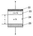
- FIG. 1 is a cross-sectional view illustrating a cross-section structure of a photosensor used in a photosensor array according to a first embodiment
- FIG. 2 is a circuit diagram illustrating an equivalent circuit of the photosensor illustrated in FIG. 1 ;
- FIG. 3 is a graph illustrating an example of a relationship between a thickness and photoconduction of an amorphous silicon film
- FIG. 4 is a diagram illustrating the operation of the photosensor according to the first embodiment
- FIG. 5 is a graph illustrating a current to voltage characteristic of a general diode
- FIG. 6 is a block diagram illustrating a structure of a photosensor array according to the first embodiment
- FIG. 7 is a circuit diagram illustrating a circuit configuration of the photosensor array according to the first embodiment
- FIG. 8 is a timing chart illustrating a method of driving the photosensor array according to the first embodiment
- FIG. 9 is a circuit diagram illustrating a circuit configuration of a photosensor array according to a second embodiment
- FIG. 10 is a timing chart illustrating the operation of the photosensor array according to the second embodiment
- FIG. 11 is a circuit diagram illustrating a circuit configuration of a photosensor array according to a third embodiment
- FIG. 12 is a block diagram illustrating an example of a signal processing circuit that corrects a dark current component
- FIG. 13 is a circuit diagram illustrating a circuit configuration of a photosensor array according to the invention in Japanese Patent Application that has been already filed in Japanese Patent Office;
- FIG. 14 is a diagram illustrating a configuration of a light-dependent variable resistance element in a photosensor illustrated in FIG. 13 ;
- FIG. 15 is a circuit diagram illustrating an equivalent circuit of the light-dependent variable resistance element ASI illustrated in FIG. 13 ;
- FIG. 16 is a timing chart illustrating the operation of the photosensor array illustrated in FIG. 13 .
- an amorphous silicon film (a-Si) and an n-type amorphous silicon film (n+a-Si) doped with phosphorus are used as a photosensor element.
- FIG. 1 is a cross-sectional view illustrating a cross-section structure of a photosensor for one pixel used in a photosensor array according to a first embodiment of the present invention.
- a photosensor according to this embodiment includes a lower electrode 25 , an amorphous silicon film (a-Si) 24 that is stacked on the lower electrode 25 , an n-type amorphous silicon film (n+a-Si) 23 that is stacked on the amorphous silicon film (a-Si) 24 and doped with phosphorus, and an upper electrode 22 disposed on the n-type amorphous silicon film (n+a-Si) 23 doped with phosphorus.
- the n-type amorphous silicon film (n+a-Si) 23 doped with phosphorus and the amorphous silicon film (a-Si) 24 are held between the upper electrode 22 and the lower electrode 25 .
- the material of the upper electrode 22 and the lower electrode 25 is so selected as to make an ohmic connection with the amorphous silicon film (a-Si) 24 and the n-type amorphous silicon film (n+a-Si) 23 doped with phosphorus, respectively, or make an ohmic connection in a forward bias direction that will be described later. Also, because this configuration is used as the photosensor, there is a need to select the electrode on a light incident side which transmits a light of a desired wavelength.
- the upper electrode 22 is made of ITO (indium tin oxide), and the lower electrode 25 is made of MoW/Al—Si/MoW. The same is applied to a cross-section structure of the photosensor according to other embodiments which will be described below.
- FIG. 2 is a circuit diagram illustrating an equivalent circuit of the photosensor illustrated in FIG. 1 .
- the n-type amorphous silicon film (n+a-Si) 23 doped with phosphorus is an n-type semiconductor higher in impurity concentration than the amorphous silicon film (a-Si) 24 . Therefore, a junction plane of the n-type amorphous silicon film (n+a-Si) 23 doped with phosphorus and the amorphous silicon film (a-Si) 24 exhibits a diode characteristic having an anode at the amorphous silicon film (a-Si) 24 side and a cathode at the n-type amorphous silicon film (n+a-Si) 23 side.
- amorphous silicon film (a-Si)
- electrons are excited to produce electron-hole pairs, and conduction carriers increase to increase a current. That is, the amorphous silicon film (a-Si) forms a variable resistance that is changed according to light. This is a phenomenon called photoconduction.
- a thickness t of the amorphous silicon film (a-Si) 24 is an important factor.
- FIG. 3 is a graph illustrating one example of a relationship between the thickness t and the photoconduction of the amorphous silicon film (a-Si) 24 .
- symbol A represents a relationship between the thickness t and the photoconduction of the amorphous silicon film (a-Si) when the amorphous silicon film (a-Si) is irradiated with light
- B represents a relationship between the thickness t and the photoconduction of the amorphous silicon film (a-Si) when the amorphous silicon film (a-Si) is not irradiated with light.
- the thickness of the amorphous silicon film (a-Si) is as thin as 170 nm, the resistance of the amorphous silicon film (a-Si) is low, and a current (bias current or dark current) that flows in a state where the amorphous silicon film (a-Si) is not irradiated with light, that is, in a dark state is large. Therefore, a current increase attributable to a change in resistance caused by the photoconduction at the time of light irradiation is buried in the bias current, and cannot be observed (separated).
- a resistance in the thickness direction becomes larger, and the bias current is decreased.
- a difference occurs between the current increase attributable to the change in resistance caused by the photoconduction at the time of light irradiation, and the bias current. This difference depends on the amount of light.
- This structure can be used as the photosensor by measurement of this difference.
- FIG. 4 is a diagram illustrating voltages applied to a diode part D and a light-dependent variable resistance part AS of the photosensor in the amorphous silicon film (a-Si). It is assumed that the voltages applied to the diode part D and the light-dependent variable resistance part AS in a state where the bias current of the dark state flows in the photosensor are Vd and Vr, respectively. In this example, it is assumed that Vd+Vr are constant (VD).
- FIG. 5 illustrates a current to voltage characteristic of a general diode.
- increase in the forward voltage precipitously increases a current with respect to the voltage change.
- the current increase is equivalent to that conduction carriers are implanted into the light-dependent variable resistance part AS of the amorphous silicon film (a-Si). Therefore, the effective resistance of the light-dependent variable resistance part AS of the amorphous silicon film (a-Si) is further decreased.
- the n-type amorphous silicon film (n+a-Si) doped with phosphorus is stacked on the amorphous silicon film (a-Si), thereby being capable of obtaining a photocurrent amplified by the diode configured by the n-type amorphous silicon film (n+a-Si) doped with phosphorus and the amorphous silicon film (a-Si).
- a structure in which the n-type amorphous silicon film (n+a-Si) doped with phosphorus is stacked on the amorphous silicon film (a-Si) has a current amplifying effect which is about 10000 times as large as that in a structure having only the amorphous silicon film (a-Si).
- FIG. 6 is a block diagram illustrating a structure of a photosensor array according to the first embodiment. The same is applied to the configuration of the photosensor array according to other embodiments described below.
- a photosensor array part 11 is disposed in the center of the photosensor array, a shift register 12 that sequentially supplies read pulses for reading the detection results of the photosensor pixels is disposed at a left side of the periphery of the photosensor array part 11 , and a bonding pad part 13 that connects to the external is disposed at a lower side of the periphery of the photosensor array part 11 .
- the photosensor array part 11 is configured by, for example, the photosensors of 100 ⁇ 150 which are arranged in a matrix.
- the respective photosensor pixels of the photosensor array part 11 are the photosensors illustrated in FIG. 1 .
- FIG. 7 is a circuit diagram illustrating a circuit configuration of a photosensor array according to the first embodiment.
- the photosensor pixels PX 1 to PX 4 are arranged in a matrix.
- FIG. 7 illustrates only four photosensor pixels of PX 1 to PX 4 , but in fact, for example, (100 ⁇ 150) photosensor pixels may be arranged.
- Each of the photosensor pixels PX 1 to PX 4 is of a structure in which the n-type amorphous silicon film (n+a-Si) 23 doped with phosphorus and the amorphous silicon film (a-Si) 24 are held between the upper electrode 22 and the lower electrode 25 .
- the photosensor pixels PX 1 to PX 4 are illustrated by the equivalent circuit illustrated in FIG. 2 .
- the cathodes of the diode parts D in each row of the photosensor pixels PX 1 to PX 4 are connected to any one of the plural scanning lines G 1 , G 2 , which corresponds to that row.
- the respective scanning lines G 1 , G 2 are connected to the shift register 12 .
- the shift register 12 sequentially applies the selection scanning voltage of Low level (hereinafter referred to as L level) to the scanning lines G 1 , G 2 , every one horizontal scanning period.
- L level Low level
- the light-dependent variable resistance parts AS in each column of the photosensors PX 1 to PX 4 are connected to any one of the plural read lines S 1 , S 2 , which corresponds to that column.
- Each voltage change in the read lines S 1 , S 2 , in one horizontal scanning period is output from the bonding pad part 13 to the external signal processing circuit (not shown) as the signal voltage.
- the shift register 12 is configured by a circuit mounted in the semiconductor chip, and arranged on a substrate where the photosensor array is fabricated.
- the shift register 12 is configured by a circuit including thin-film transistors in which a semiconductor layer is formed of a polysilicon layer on a photosensor array substrate such as a glass substrate.
- the respective reset transistors TLS are disposed between the read lines S 1 , S 2 , and a wire through which a reset voltage VRST is applied, and controlled according to a signal RG. Also, the stray capacitance Cs is developed between each read line and the external wire.
- FIG. 8 is a timing chart illustrating a method of driving the photosensor array according to this embodiment.
- the method of driving the photosensor array according to this embodiment will be described with reference to FIG. 8 .
- the respective rows of the photosensor pixels are sequentially scanned downward by the shift register 12 . That is, in FIG. 7 , it is assumed that a voltage of L level is sequentially applied to gate lines G in the increasing order of number.
- a signal RG becomes high level (hereinafter referred to as H level), and reset transistors TLS turn on.
- H level high level
- reset transistors TLS turn on.
- respective read lines S 1 , S 2 are reset, and the respective read lines S 1 , S 2 , are uniformly set to a fixed potential (for example, 3V).
- the respective scanning lines G 1 , G 2 are H level (for example, 3V).
- the signal RG becomes L level
- the voltage of a scanning line G 1 becomes low level (hereinafter referred to as L level, for example, ground potential of 0V)
- the voltage of the other scanning levels becomes H level.
- L level for example, ground potential of 0V
- the diode part D having cathodes connected to the scanning line G 1 become on
- the diode parts D having cathodes connected to the scanning lines other than the scanning line G 1 become off. Therefore, the photosensor pixels PX 1 and PX 2 become on, and the photosensor pixels PX 3 and PX 4 become off.
- the photosensor pixel PX 2 when it is assumed that the photosensor pixel PX 2 is irradiated with light, and the photosensor pixel PX 1 is not irradiated with light, a dark current flows due to the resistance value of the light-dependent variable resistance part AS in the photosensor pixel PX 1 . Therefore the potential of the read line S 1 is lowered to, for example, 2.5V.
- the resistance value of the light-dependent variable resistance part AS in the photosensor pixel PX 2 that has been irradiated with light allows a current to be amplified by photoconduction. Therefore the potential of the read line S 2 is lowered to, for example, 1.5V.
- This voltage change is read as the signal voltages of the respective read lines S 1 , S 2 .
- a waveform of the read line S 1 ⁇ in FIG. 8 shows the voltage change.
- the potentials of the respective read lines S 1 , S 2 are uniformly set to the fixed potential (for example, 3V), and thereafter the potentials of the respective read lines S 1 , S 2 , are fluctuated by the incident light (descent in FIG. 8 ).
- the signal RG becomes H level, and the reset transistors TLS turn on.
- the respective read lines S 1 , S 2 are reset, and the respective read lines S 1 , S 2 , are uniformly set to the fixed potential (for example, 3V).
- the voltage of the scanning line G 2 becomes L level, and the voltage of the other scanning lines becomes H level.
- the diode parts D having a cathode connected to the scanning line G 2 becomes on, and the diode parts D having the cathodes connected to the scanning lines other than the scanning line G 2 become off. Therefore, the photosensor pixels PX 1 and PX 2 become off, and the photosensor pixels PX 3 and PX 4 become on.
- FIG. 9 is a circuit diagram illustrating a circuit configuration of a photosensor array according to a second embodiment.
- FIG. 10 is a timing chart illustrating a method of driving the photosensor array according to the second embodiment.
- This embodiment is mainly different from the above-described first embodiment in that the photosensor pixels are reversely connected.
- the polarities of the drive voltage and the signal voltage are also reverse. That is, in the method of driving the photosensor array according to this embodiment, when, in the blanking period of one horizontal scanning period HSYNC, the signal RG becomes H level, and the reset transistors TLS turn on, the respective read lines S 1 , S 2 , are uniformly set to aground potential.
- the signal RG becomes H level, and the reset transistors TLS turn on.
- the respective read lines S 1 , S 2 are reset, and the respective read lines S 1 , S 2 , are uniformly set to the fixed potential (for example, the ground potential of 0V).
- the respective scanning lines G 1 , G 2 become L level (for example, 0V).
- the voltage of the scanning line G 1 becomes H level (for example, 3V), and the voltage of the other scanning lines becomes L level.
- the diode parts D having the anode connected to the scanning line G 1 through the light-dependent variable resistance part AS become on, and the diode parts D having the anodes connected to the scanning lines other than the scanning line G 1 through the light-dependent variable resistance parts AS become off. Therefore, the photosensor pixels PX 1 an PX 2 become on, and the photosensor pixels PX 3 an PX 4 become off.
- the potential of the read line S 1 is increased to, for example, 0.5V.
- the resistance value of the light-dependent variable resistance part AS in the photosensor pixel PX 2 which has been irradiated with light allows a current to be amplified by photoconduction. Therefore the potential of the read line S 2 increases up to, for example, 1.5V. This voltage change is read as the signal voltages of the respective read lines S 1 , S 2 .
- the potentials of the respective read lines S 1 , S 2 are uniformly set to the fixed potential (for example, ground potential of 0V) in timing when the signal RG becomes H level, the potentials of the respective read lines S 1 , S 2 , are allowed to fluctuate (increase in FIG. 8 ) due to the incident light.
- the fixed potential for example, ground potential of 0V
- an external signal processing circuit connected to the bonding pad part 13 takes in this signal voltage.
- the signal RG becomes H level, and the reset transistors TLS turn on.
- the respective read lines S 1 , S 2 are reset, and the respective read lines S 1 , S 2 , are uniformly set to the fixed potential (for example, the ground potential of 0V).
- the voltage of the scanning line G 2 becomes H level, and the voltage other than the other scanning lines becomes L level.
- the diode parts D having the anode connected to the scanning line G 2 through the light-dependent variable resistance part AS become on, and the diode parts D having the anodes connected to the scanning lines other than the scanning line G 2 through the light-dependent variable resistance parts AS become off. Therefore, the photosensor pixels PX 1 an PX 2 become off, and the photosensor pixels PX 3 an PX 4 become on.
- a relatively large dark current component is always contained in the output signal voltage (or current). Also, because the dark current of amorphous silicon that is a high-resistant semiconductor has a temperature dependency, there is a need to correct the dark current component under the usage environment.
- the photosensor array according to this embodiment is configured to correct the dark current component.
- FIG. 11 is a circuit diagram illustrating a circuit configuration of a photosensor array according to a third embodiment.
- a difference between this embodiment and the first embodiment mainly resides in that a photosensor pixel PXD for dark current correction is disposed on each row of the photosensor array.
- the photosensor pixel PXD for dark current correction may be disposed in the photosensor array of the second embodiment.
- one photosensor PXD for dark current correction is disposed on each row of the photosensor array.
- the photosensors PXD for dark current correction on one column are disposed at an opposite end of the shift register 12 in the photosensor array.
- a cross-section structure of the photosensors PXD for dark current correction is identical with the cross-section structure illustrated in FIG. 1 .
- a light blocking film is disposed on each of the photosensors PXD for dark current correction so as to prevent light incidence.
- a method of driving the photosensor array in this embodiment is identical with that in FIG. 8 , but a signal voltage of the photosensor PXD for dark current correction is output from the read line SD for dark current correction.
- a dark state is produced under the usage environment, and a process of subtracting this voltage from an output during light irradiation is executed by the external signal processing circuit, and the dark current component is corrected.
- FIG. 12 is a block diagram illustrating an example of an external signal processing circuit that corrects a dark current component.
- the signal processing circuit illustrated in FIG. 12 inputs the signal voltages (Sn-V) of the photosensor pixels on each row, which are read from the respective read lines S 1 , S 2 , in the photosensor array, and the signal voltages (SD-V) of the photosensor pixels PXD, which are read from the read line SD for dark current correction, to an A/D converter 31 through a buffer circuit BA, and converts the input voltages into digital signals. Thereafter, a subtractor 32 subtracts the digital signal voltage of the photosensor pixel PXD for dark current correction from the digital signal voltage of the photosensor pixel for each row to correct the dark current component.
- the signal processing circuit is not required to be externally provided, but may be mounted in a semiconductor chip, and arranged on a substrate where the photosensor array is fabricated as with the shift register 12 illustrated in FIG. 6 .
- the signal processing circuit may be configured by forming a circuit including thin-film transistors in which a semiconductor layer is formed of a polysilicon layer on a photosensor array substrate such as a glass substrate.
Landscapes
- Solid State Image Pick-Up Elements (AREA)
- Transforming Light Signals Into Electric Signals (AREA)
- Facsimile Heads (AREA)
Abstract
Description
Claims (12)
Applications Claiming Priority (2)
| Application Number | Priority Date | Filing Date | Title |
|---|---|---|---|
| JP2010216708A JP5654305B2 (en) | 2010-09-28 | 2010-09-28 | Photosensor array |
| JP2010-216708 | 2010-09-28 |
Publications (2)
| Publication Number | Publication Date |
|---|---|
| US20120074297A1 US20120074297A1 (en) | 2012-03-29 |
| US8963064B2 true US8963064B2 (en) | 2015-02-24 |
Family
ID=45869688
Family Applications (1)
| Application Number | Title | Priority Date | Filing Date |
|---|---|---|---|
| US13/239,754 Active 2032-12-09 US8963064B2 (en) | 2010-09-28 | 2011-09-22 | Photosensor having upper and lower electrodes with amorphous silicon film and n-type amorphous silicon film therebetween and photosensor array |
Country Status (3)
| Country | Link |
|---|---|
| US (1) | US8963064B2 (en) |
| JP (1) | JP5654305B2 (en) |
| CN (1) | CN102569309B (en) |
Families Citing this family (4)
| Publication number | Priority date | Publication date | Assignee | Title |
|---|---|---|---|---|
| WO2011116345A1 (en) | 2010-03-19 | 2011-09-22 | Invisage Technologies, Inc. | Dark current reduction in image sensors via dynamic electrical biasing |
| KR101941984B1 (en) * | 2011-09-27 | 2019-04-12 | 삼성디스플레이 주식회사 | Liquid crystal display device |
| US10104322B2 (en) | 2014-07-31 | 2018-10-16 | Invisage Technologies, Inc. | Image sensors with noise reduction |
| US10425601B1 (en) | 2017-05-05 | 2019-09-24 | Invisage Technologies, Inc. | Three-transistor active reset pixel |
Citations (5)
| Publication number | Priority date | Publication date | Assignee | Title |
|---|---|---|---|---|
| US5023443A (en) * | 1989-01-18 | 1991-06-11 | Konica Corporation | Image sensor and its driving method |
| JPH1197660A (en) | 1997-09-19 | 1999-04-09 | Semiconductor Energy Lab Co Ltd | Image sensor and device utilizing the same |
| US20060113484A1 (en) * | 2003-12-05 | 2006-06-01 | Canon Kabushiki Kaisha | Radiation image pick-up device and radiation image pick-up method |
| JP2010011033A (en) | 2008-06-26 | 2010-01-14 | Epson Imaging Devices Corp | Photoelectric converting device and radiation detecting device |
| US20110006192A1 (en) | 2009-07-09 | 2011-01-13 | Hitachi Dispalys, Ltd. | Optical sensor array and optical sensor circuit |
Family Cites Families (3)
| Publication number | Priority date | Publication date | Assignee | Title |
|---|---|---|---|---|
| US6818899B2 (en) * | 2001-06-07 | 2004-11-16 | Canon Kabushiki Kaisha | Radiographic image pickup apparatus and method of driving the apparatus |
| JP4277619B2 (en) * | 2003-08-18 | 2009-06-10 | 三菱電機株式会社 | Solid-state image sensor |
| JP4847202B2 (en) * | 2006-04-27 | 2011-12-28 | キヤノン株式会社 | Imaging apparatus and radiation imaging system |
-
2010
- 2010-09-28 JP JP2010216708A patent/JP5654305B2/en active Active
-
2011
- 2011-09-22 US US13/239,754 patent/US8963064B2/en active Active
- 2011-09-27 CN CN201110294301.6A patent/CN102569309B/en active Active
Patent Citations (7)
| Publication number | Priority date | Publication date | Assignee | Title |
|---|---|---|---|---|
| US5023443A (en) * | 1989-01-18 | 1991-06-11 | Konica Corporation | Image sensor and its driving method |
| JPH1197660A (en) | 1997-09-19 | 1999-04-09 | Semiconductor Energy Lab Co Ltd | Image sensor and device utilizing the same |
| US20060113484A1 (en) * | 2003-12-05 | 2006-06-01 | Canon Kabushiki Kaisha | Radiation image pick-up device and radiation image pick-up method |
| CN1890957A (en) | 2003-12-05 | 2007-01-03 | 佳能株式会社 | Radiation image pick-up device and radiation image pick-up method |
| JP2010011033A (en) | 2008-06-26 | 2010-01-14 | Epson Imaging Devices Corp | Photoelectric converting device and radiation detecting device |
| US20110006192A1 (en) | 2009-07-09 | 2011-01-13 | Hitachi Dispalys, Ltd. | Optical sensor array and optical sensor circuit |
| JP2011019102A (en) | 2009-07-09 | 2011-01-27 | Hitachi Displays Ltd | Optical sensor circuit, and optical sensor array |
Non-Patent Citations (2)
| Title |
|---|
| English translation of Chinese Patent Office Action in Chinese Patent Application No. 201110294301.6, dated Apr. 2, 2014. |
| English translation of Office Action in corresponding Japanese Patent Application No. 2010-216708, dated Feb. 4, 2014. |
Also Published As
| Publication number | Publication date |
|---|---|
| CN102569309B (en) | 2015-08-26 |
| JP5654305B2 (en) | 2015-01-14 |
| JP2012074448A (en) | 2012-04-12 |
| CN102569309A (en) | 2012-07-11 |
| US20120074297A1 (en) | 2012-03-29 |
Similar Documents
| Publication | Publication Date | Title |
|---|---|---|
| US9515106B2 (en) | Radiation imaging device with metal-insulator-semiconductor photodetector and thin film transistor | |
| US8519320B2 (en) | Optical sensor circuit or array including optical sensor element having a light dependent variable resistance element | |
| KR101095720B1 (en) | Display device including an image sensor | |
| EP2027717B1 (en) | Image sensor and display | |
| US20080179495A1 (en) | Image sensor | |
| US20130100327A1 (en) | Image pickup unit and image pickup display system | |
| US11558567B2 (en) | Optical active pixel sensor using TFT pixel circuit | |
| US20160360132A1 (en) | Imaging device including pixels | |
| CN114615445A (en) | Phototransistor and photosensitive method thereof | |
| US8963064B2 (en) | Photosensor having upper and lower electrodes with amorphous silicon film and n-type amorphous silicon film therebetween and photosensor array | |
| EP1850387B1 (en) | Solid-state image pickup device | |
| US10091444B2 (en) | Photoelectric conversion apparatus and photoelectric conversion system | |
| US10136075B2 (en) | Compensation circuit for an x-ray detector | |
| US8748792B2 (en) | Photosensor and photosensor array with capacitive element | |
| JPH10189934A (en) | Photoelectric conversion device and driving method thereof | |
| JP5061687B2 (en) | Photosensor, photosensor array, photosensor system, and drive control method for photosensor system | |
| US20050007473A1 (en) | Reducing image sensor lag | |
| KR20200082122A (en) | Digital x-ray detector and method for driving the same | |
| WO2022210070A1 (en) | Solid-state imaging element | |
| US20240259708A1 (en) | Imaging device | |
| US8576314B2 (en) | Photosensor device | |
| KR20250054654A (en) | X-ray detector |
Legal Events
| Date | Code | Title | Description |
|---|---|---|---|
| AS | Assignment |
Owner name: PANASONIC LIQUID CRYSTAL DISPLAY CO., LTD., JAPAN Free format text: ASSIGNMENT OF ASSIGNORS INTEREST;ASSIGNORS:YONEKURA, TAKESHI;MIYAZAWA, TOSHIO;HASEGAWA, ATSUSHI;AND OTHERS;SIGNING DATES FROM 20110902 TO 20110906;REEL/FRAME:026947/0597 Owner name: HITACHI DISPLAYS, LTD., JAPAN Free format text: ASSIGNMENT OF ASSIGNORS INTEREST;ASSIGNORS:YONEKURA, TAKESHI;MIYAZAWA, TOSHIO;HASEGAWA, ATSUSHI;AND OTHERS;SIGNING DATES FROM 20110902 TO 20110906;REEL/FRAME:026947/0597 |
|
| AS | Assignment |
Owner name: JAPAN DISPLAY EAST, INC., JAPAN Free format text: CHANGE OF NAME;ASSIGNOR:HITACHI DISPLAYS, LTD.;REEL/FRAME:032464/0765 Effective date: 20120401 Owner name: JAPAN DISPLAY INC., JAPAN Free format text: CHANGE OF NAME;ASSIGNOR:JAPAN DISPLAY EAST, INC.;REEL/FRAME:032465/0081 Effective date: 20130401 |
|
| STCF | Information on status: patent grant |
Free format text: PATENTED CASE |
|
| FEPP | Fee payment procedure |
Free format text: PAYOR NUMBER ASSIGNED (ORIGINAL EVENT CODE: ASPN); ENTITY STATUS OF PATENT OWNER: LARGE ENTITY |
|
| MAFP | Maintenance fee payment |
Free format text: PAYMENT OF MAINTENANCE FEE, 4TH YEAR, LARGE ENTITY (ORIGINAL EVENT CODE: M1551) Year of fee payment: 4 |
|
| MAFP | Maintenance fee payment |
Free format text: PAYMENT OF MAINTENANCE FEE, 8TH YEAR, LARGE ENTITY (ORIGINAL EVENT CODE: M1552); ENTITY STATUS OF PATENT OWNER: LARGE ENTITY Year of fee payment: 8 |
|
| AS | Assignment |
Owner name: PANASONIC INTELLECTUAL PROPERTY CORPORATION OF AMERICA, CALIFORNIA Free format text: NUNC PRO TUNC ASSIGNMENT;ASSIGNOR:PANASONIC LIQUID CRYSTAL DISPLAY CO., LTD.;REEL/FRAME:065615/0327 Effective date: 20230828 |
|
| AS | Assignment |
Owner name: MAGNOLIA PURPLE CORPORATION, JAPAN Free format text: ASSIGNMENT OF ASSIGNORS INTEREST;ASSIGNOR:JAPAN DISPLAY INC;REEL/FRAME:071890/0202 Effective date: 20250625 |