US8958708B2 - Image forming apparatus having variable potential setting - Google Patents
Image forming apparatus having variable potential setting Download PDFInfo
- Publication number
- US8958708B2 US8958708B2 US13/465,373 US201213465373A US8958708B2 US 8958708 B2 US8958708 B2 US 8958708B2 US 201213465373 A US201213465373 A US 201213465373A US 8958708 B2 US8958708 B2 US 8958708B2
- Authority
- US
- United States
- Prior art keywords
- transfer
- photosensitive member
- image forming
- potential
- charged
- Prior art date
- Legal status (The legal status is an assumption and is not a legal conclusion. Google has not performed a legal analysis and makes no representation as to the accuracy of the status listed.)
- Expired - Fee Related, expires
Links
Images


Classifications
-
- G—PHYSICS
- G03—PHOTOGRAPHY; CINEMATOGRAPHY; ANALOGOUS TECHNIQUES USING WAVES OTHER THAN OPTICAL WAVES; ELECTROGRAPHY; HOLOGRAPHY
- G03G—ELECTROGRAPHY; ELECTROPHOTOGRAPHY; MAGNETOGRAPHY
- G03G15/00—Apparatus for electrographic processes using a charge pattern
- G03G15/04—Apparatus for electrographic processes using a charge pattern for exposing, i.e. imagewise exposure by optically projecting the original image on a photoconductive recording material
- G03G15/043—Apparatus for electrographic processes using a charge pattern for exposing, i.e. imagewise exposure by optically projecting the original image on a photoconductive recording material with means for controlling illumination or exposure
-
- G—PHYSICS
- G03—PHOTOGRAPHY; CINEMATOGRAPHY; ANALOGOUS TECHNIQUES USING WAVES OTHER THAN OPTICAL WAVES; ELECTROGRAPHY; HOLOGRAPHY
- G03G—ELECTROGRAPHY; ELECTROPHOTOGRAPHY; MAGNETOGRAPHY
- G03G15/00—Apparatus for electrographic processes using a charge pattern
- G03G15/01—Apparatus for electrographic processes using a charge pattern for producing multicoloured copies
- G03G15/0105—Details of unit
- G03G15/0131—Details of unit for transferring a pattern to a second base
-
- G—PHYSICS
- G03—PHOTOGRAPHY; CINEMATOGRAPHY; ANALOGOUS TECHNIQUES USING WAVES OTHER THAN OPTICAL WAVES; ELECTROGRAPHY; HOLOGRAPHY
- G03G—ELECTROGRAPHY; ELECTROPHOTOGRAPHY; MAGNETOGRAPHY
- G03G15/00—Apparatus for electrographic processes using a charge pattern
- G03G15/01—Apparatus for electrographic processes using a charge pattern for producing multicoloured copies
- G03G15/0142—Structure of complete machines
- G03G15/0178—Structure of complete machines using more than one reusable electrographic recording member, e.g. one for every monocolour image
- G03G15/0189—Structure of complete machines using more than one reusable electrographic recording member, e.g. one for every monocolour image primary transfer to an intermediate transfer belt
-
- G—PHYSICS
- G03—PHOTOGRAPHY; CINEMATOGRAPHY; ANALOGOUS TECHNIQUES USING WAVES OTHER THAN OPTICAL WAVES; ELECTROGRAPHY; HOLOGRAPHY
- G03G—ELECTROGRAPHY; ELECTROPHOTOGRAPHY; MAGNETOGRAPHY
- G03G15/00—Apparatus for electrographic processes using a charge pattern
- G03G15/14—Apparatus for electrographic processes using a charge pattern for transferring a pattern to a second base
- G03G15/16—Apparatus for electrographic processes using a charge pattern for transferring a pattern to a second base of a toner pattern, e.g. a powder pattern, e.g. magnetic transfer
- G03G15/1665—Apparatus for electrographic processes using a charge pattern for transferring a pattern to a second base of a toner pattern, e.g. a powder pattern, e.g. magnetic transfer by introducing the second base in the nip formed by the recording member and at least one transfer member, e.g. in combination with bias or heat
- G03G15/167—Apparatus for electrographic processes using a charge pattern for transferring a pattern to a second base of a toner pattern, e.g. a powder pattern, e.g. magnetic transfer by introducing the second base in the nip formed by the recording member and at least one transfer member, e.g. in combination with bias or heat at least one of the recording member or the transfer member being rotatable during the transfer
- G03G15/1675—Apparatus for electrographic processes using a charge pattern for transferring a pattern to a second base of a toner pattern, e.g. a powder pattern, e.g. magnetic transfer by introducing the second base in the nip formed by the recording member and at least one transfer member, e.g. in combination with bias or heat at least one of the recording member or the transfer member being rotatable during the transfer with means for controlling the bias applied in the transfer nip
-
- G—PHYSICS
- G03—PHOTOGRAPHY; CINEMATOGRAPHY; ANALOGOUS TECHNIQUES USING WAVES OTHER THAN OPTICAL WAVES; ELECTROGRAPHY; HOLOGRAPHY
- G03G—ELECTROGRAPHY; ELECTROPHOTOGRAPHY; MAGNETOGRAPHY
- G03G2215/00—Apparatus for electrophotographic processes
- G03G2215/01—Apparatus for electrophotographic processes for producing multicoloured copies
- G03G2215/0103—Plural electrographic recording members
- G03G2215/0119—Linear arrangement adjacent plural transfer points
- G03G2215/0122—Linear arrangement adjacent plural transfer points primary transfer to an intermediate transfer belt
- G03G2215/0125—Linear arrangement adjacent plural transfer points primary transfer to an intermediate transfer belt the linear arrangement being horizontal or slanted
- G03G2215/0129—Linear arrangement adjacent plural transfer points primary transfer to an intermediate transfer belt the linear arrangement being horizontal or slanted horizontal medium transport path at the secondary transfer
Definitions
- the present invention relates to an image forming apparatus of an electrophotographic type, such as a copying machine, a printer, a facsimile machine, or a multi-function machine of these machines, in which a plurality of image forming portions are provided.
- an intended image is visualized as a toner image by subjecting a surface of a photosensitive drum to an image forming process including steps of charging, exposure, development and the like and then the toner image is transferred onto a transfer material in a transfer step has been known.
- a structure in which a full-color image can be obtained by superposing toner images of a plurality of colors has also been conventionally known.
- this structure there is, e.g., a structure in which a plurality of image forming portions (image forming stations) are provided and toner images formed at the respective image forming portions are successively transferred onto the transfer material such as an intermediary transfer belt or a recording material.
- a resistance is fluctuated depending on an environment at the transfer portion.
- the transfer portion is constituted by nipping the intermediary transfer belt between a transfer roller and the photosensitive drum but it has been known that the resistance of the transfer roller or the intermediary transfer belt is fluctuated depending on a temperature and humidity in an ambient condition, the number of sheets subjected to image formation, or the like.
- the transfer voltage value is set depending on these resistance fluctuations.
- a full-color image forming apparatus of a tandem type in order to effect image formation for a plurality of colors (e.g., four colors), a plurality of pairs (e.g., four pairs) of a developing device and a transfer means are needed.
- Driving devices for driving these developing devices and transfer means are connected to a high-voltage power sources (high-voltage sources) for each of the colors. Therefore, a plurality of power sources are required, so that a cost is increased.
- an output current value with respect to a value of a constant voltage applied to the transfer roller is different at each of the image forming stations.
- the output current value is outside of a proper range, there is a possibility of an occurrence of improper transfer or image defect due to abnormal electric discharge.
- a principal object of the present invention is to provide an image forming apparatus capable of reducing a degree of an occurrence of improper transfer or image defect due to abnormal electric discharge, in which commonalty of a transfer power source is realized.
- Another object of the present invention is to provide an image forming apparatus, in which commonality of the transfer power source is realized, capable of reducing the degree of the occurrence of the improper transfer or the image defect due to the abnormal electric discharge by passing an optimum current through each of a first transfer means and a second transfer means even in the case where a resistance value or the like is different between the first transfer means and the second transfer means.
- an image forming apparatus comprising: a first image forming portion including a first photosensitive member, first charging means for electrically charging the first photosensitive member, first exposure means for exposing to light the charged first photosensitive member to form an electrostatic latent image, first developing means for forming a toner image by depositing a toner on an exposed portion of the electrostatic latent image, and first transfer means for transferring the toner image from the first photosensitive member onto a transfer material; a second image forming portion including a second photosensitive member, second charging means for electrically charging the second photosensitive member, second exposure means for exposing to light the charged second photosensitive member to form an electrostatic latent image, second developing means for forming a toner image by depositing a toner on an exposed portion of the electrostatic latent image, and second transfer means for transferring the toner image from the second photosensitive member onto the transfer material; a power source for applying a common voltage to the first transfer means and the second transfer means; and setting means for variably setting
- FIG. 1 is a schematic illustration of an image forming apparatus according to an embodiment of the present invention.
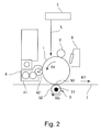
- FIG. 2 is a schematic illustration of an image forming portion.
- FIG. 3 is a graph showing a relationship between a transfer voltage and a current.
- FIG. 4 is a graph for illustrating a transfer contrast.
- FIG. 5 is a flow chart of image formation in the embodiment.
- Embodiments of the present invention will be described with reference to FIGS. 1 to 5 .
- An image forming apparatus 100 is a full-color laser printer or a tandem type in which a plurality of image forming portions Pa, Pb, Pc and Pd for magenta (M), cyan (C), yellow (Y) and black (K), respectively are provided along an intermediary transfer belt 7 as a transfer material.
- M magenta
- C cyan
- Y yellow
- K black
- any combination of two of all the image forming portions Pa, Pb, Pc and Pc provides a relationship between a first image forming portion and a second image forming portion.
- toner images of magenta, cyan, yellow and black, respectively are formed.
- the respective image forming portions have the same constitution except that the colors of the toners used in developing devices 4 a , 4 b , 4 c and 4 d are different from each other. Therefore, in FIG. 2 , suffixes, a, b, c and d for discriminating the four image forming portions are omitted and the constitution and operation will be collectively described.
- a photosensitive drum 1 (photosensitive member) provided at the image forming portion P is rotationally driven in an arrow R 1 direction at a process speed (peripheral speed) of, e.g., 100 mm/sec by a driving means (not shown).
- a charging roller 2 Around the photosensitive drum 1 , along a rotational direction of the photosensitive drum 1 , a charging roller 2 , an exposure device 3 , the developing device 4 , a primary transfer roller 5 and a cleaning device 6 are provided substantially in this order.
- the charging roller is a charging means.
- the exposure device 3 corresponds to an exposure means.
- the developing device 4 corresponds to a developing means.
- the primary transfer roller 5 corresponds to a transfer means.
- the charging roller 2 and the exposure device 3 constitute an electrostatic latent image forming means.
- the rotationally driven photosensitive drum 1 is charged at its surface by the charging roller 2 by applying a voltage to the charging roller 2 .
- the charging roller 2 is contacted to the surface of the photosensitive drum 1 , and a charging bias is applied to the charging roller 2 by a charging bias application voltage (power) source (not shown).
- a charging bias application voltage (power) source not shown.
- the surface of the photosensitive drum 1 is uniformly charged to, e.g., ⁇ 600 V.
- the charging bias application voltage source is provided for each of the stations (image forming portions) and is capable of applying an arbitrary charging bias without being limited to ⁇ 600 V.
- an electrostatic latent image is formed by the exposure device 3 .
- the exposure device 3 emits laser light L on the basis of image information, so that the surface of the photosensitive drum 1 is exposed to the laser light L.
- the surface of the photosensitive drum 1 after being charged is subjected to removal of the electric charge at an exposed portion, so that the electrostatic latent image is formed. Also an output of the laser light L of the exposure device 3 is settable.
- the developing device 4 includes a developing container 41 for accommodating a two-component developer containing non-magnetic toner particles (toner) and a magnetic carrier (carrier) in mixture. The developer is stirred in the developing container 41 , so that the non-magnetic toner particles are negatively charged.
- the developer is carried on a developing sleeve 42 rotating in an arrow R 4 direction.
- a developing bias including a negative DC component is applied to the developing sleeve 42 by a developing bias voltage (power) source (not shown)
- the non-magnetic toner particles carried on the surface of the developing sleeve 42 are transferred onto the electrostatic latent image formed on the surface of the photosensitive drum 1 , thus developing the electrostatic latent image as a toner image.
- the toner image formed on the photosensitive drum 1 is primary-transferred onto an intermediary transfer belt 7 (transfer material) by the primary transfer roller 5 to which a positive transfer voltage is applied.
- the toner image formed on the photosensitive drum 1 c of the image forming portion Pc is primary-transferred onto the intermediary transfer belt 7 .
- the toner image formed on the photosensitive drum 1 d of the image forming portion Pd is primary-transferred onto the intermediary transfer belt 7 .
- the primary transfer roller 5 is constituted by providing a cylindrical electroconductive layer 52 on an outer peripheral surface of a metal shaft 51 .
- the primary transfer roller 5 is, e.g., 16 mm in diameter and, e.g., 1 ⁇ 10 7 ⁇ in resistance value. This resistance value was measured by placing the primary transfer roller 5 on a metal plate and thereby applying a voltage of 50 V between the plate and the shaft 51 .
- all the resistance values of the primary transfer rollers 5 are substantially equal to each other.
- the resistance value of the primary transfer roller 5 is not limited to the above value but can be in a range of 1 ⁇ 10 5 ⁇ to 9 ⁇ 10 7 ⁇ .
- the primary transfer roller 5 urges the intermediary transfer belt 7 toward the photosensitive drum 1 .
- a primary transfer portion N 1 is formed between the surface of the photosensitive drum 1 and the surface of the intermediary transfer belt 7 .
- the primary transfer roller 5 is rotated in an arrow R 5 direction by the rotational drive of the intermediary transfer belt in an arrow R 7 direction.
- the toner image formed on the surface of the photosensitive drum 1 is primary-transferred electrostatically onto the intermediary transfer belt 7 a at the primary transfer portion N 1 by the primary transfer roller 5 to which a primary transfer voltage is applied from a primary transfer high-voltage source (power source) 54 .
- the toner images of magenta, cyan, yellow and black formed on the respective photosensitive drums 1 of the image forming portions Pa to Pd are, when the primary transfer voltage is applied to the primary transfer roller 5 at each image forming portion, successively primary-transferred superposedly onto the intermediary transfer belt 7 .
- the image forming portions are provided at an interval of, e.g., 70 mm.
- a constitution such that a common voltage is applied from the primary transfer high-voltage source 54 to the primary transfer rollers 5 a to 5 d is employed. That is, the primary transfer high-voltage source 54 applies the voltage of the same voltage to all the primary transfer rollers 5 a to 5 d .
- current detecting devices (detecting means) 53 a , 53 b , 53 c and 53 d are provided so as to detect currents passing through the primary transfer rollers 5 a to 5 d.
- the toner (residual toner) remaining on the surface of the photosensitive drum 1 without being transferred onto the intermediary transfer belt 7 during the primary transfer is removed by a cleaning blade of the cleaning device 6 .
- the photosensitive drum 1 having the cleaned surface is subjected to subsequent image formation starting from the charging.
- the photosensitive drum 1 , the charging roller 2 , the developing device 4 and the cleaning device 6 which are described above are integrally incorporated into a cartridge container (not shown) to constitute a (process) cartridge as a whole.
- This cartridge is constituted so as to be detachably mountable to an image forming apparatus main assembly and, e.g., when the photosensitive drum 1 reaches the end of its lifetime, the entire cartridge is taken out of the image forming apparatus main assembly to be replaced with a new (fresh) cartridge.
- the intermediary transfer belt 7 onto which the respective toner images are primary-transferred is constituted in an endless shape and is extended around three rollers, i.e., a driving roller 11 , a follower roller 12 and a secondary transfer opposite roller 13 as shown in FIG. 1 . Further, with rotation of the driving roller 11 in an arrow R 11 direction (in the clockwise direction in FIG. 1 ), the intermediary transfer belt 7 is moved in the arrow R 7 direction.
- the intermediary transfer belt 7 is formed, in the endless shape, of a dielectric resin material such as polyimide, polycarbonate, polyethylene terephthalate or polyvinylidene fluoride.
- the intermediary transfer belt 7 has a surface resistivity (resistance) of 1 ⁇ 10 12 ⁇ /sq.
- the surface resistivity of the intermediary transfer belt 7 is not limited to this value but can be in a range of 1 ⁇ 10 11 ⁇ /sq to 9 ⁇ 10 13 ⁇ /sq.
- the surface resistivity was measured in accordance with JIS K 6911 under application of a voltage of 100 V.
- a secondary transfer roller (secondary transfer means) 14 is contacted to the intermediary transfer belt 7 . Between this secondary transfer roller 14 and the intermediary transfer belt 7 , a secondary transfer portion (secondary transfer means) N 2 is formed.
- the secondary transfer opposite roller 13 is a metal roller and is electrically grounded.
- the secondary transfer roller 14 is prepared by forming a cylindrical electroconductive rubber around a metal shaft and has a diameter of 20 mm.
- the four color toner images which are primary transferred at the respective image forming portions and which are superposed on the intermediary transfer belt 7 are secondary-transferred onto a recording material S by the secondary transfer roller 14 . That is, to the secondary transfer roller 14 , a positive secondary transfer bias is applied from a secondary transfer bias application voltage (power) source 16 when the recording material S passes through the secondary transfer portion N 2 . As a result, the four color toner images are secondary-transferred collectively from the intermediary transfer belt 7 onto the recording material S.
- the toner (residual toner) remaining on the intermediary transfer belt 7 without being transferred onto the recording material S at this time is removed by a belt cleaner 17 provided at a position where the belt cleaner 17 opposes the follower roller 12 .
- the recording material S subjected to the image formation is accommodated in a sheet feeding cassette (not shown).
- the recording material S accommodated in the sheet feeding cassette is conveyed to registration rollers 15 by a sheet feeding and conveying device including a sheet feeding roller, a conveying roller, a conveying guide and the like (which are not shown), and oblique movement of the recording material S is corrected by the registration rollers 15 and then the recording material S is supplied to the above-described secondary transfer portion N 2 .
- the recording material S on which the toner images are secondary-transferred is, after being subjected to removal of the electric charge by a charge-removing needle 24 which is electrically grounded, conveyed to a fixing device 22 by a conveying belt 18 rotating in an arrow roller 18 direction.
- the fixing device 22 includes a fixing roller 20 in which a heater 19 is incorporated and includes a passing roller 21 urged against the fixing roller 20 to form a fixing nip.
- the recording material S is heated and pressed by the fixing roller 20 and the pressing roller 21 when the recording material S passes through the fixing nip, so that the toner images are fixed on the surface of the recording material S.
- the recording material S after being subjected to the toner image fixation is discharged to the outside of the image forming apparatus main assembly. As a result, four-color based full-color image formation on a sheet of the recording material S is ended.
- a density sensor 23 is provided so as to be opposite a surface portion of the intermediary transfer belt 7 which is extended and contacted around the driving roller 11 .
- the density sensor 23 is constituted by a reflection sensor including a light-emitting element (LED) and a light receiving element.
- a toner image for detecting a density of the color (hereinafter referred to as a “detection toner image”) is formed at each of the image forming portions Pa, Pb, Pc and Pd.
- the density sensor detects a reflected light quantity of the detection toner image. A detection result thereof is set to a density control means 25 .
- the density control means 25 computes a toner amount per unit area on the intermediary transfer belt 7 on the basis of the reflected light quantity detected by the density sensor 23 . Further, based on the computation result, a supply amount of the non-magnetic toner is controlled, so that a proportion between the magnetic carrier and the non-magnetic toner which are accommodated in the developing container 41 is changed or a potential or the like of the photosensitive drum 1 charged by the charging roller 2 is controlled.
- the primary transfer voltage is set depending on the change in resistance by using control which is called ATVC (active transfer voltage control).
- ATVC active transfer voltage control
- This ATVC is effected at each of the image forming portions but may be effected separately or collectively. In this embodiment, the ATVC is effected collectively.
- a plurality of voltages for a test different in amplitude (value) are applied to the primary transfer roller 5 .
- the ATVC is executed in, e.g., a warming-up period after power-on of the image forming apparatus until a temperature of the fixing device is increased up to a rise temperature or in a period in which a transfer operation after an end of printing on a predetermined number of sheets (e.g., 500 sheets) is not performed.
- a current passing through the primary transfer roller 5 at that time is detected by a current detecting device 53 .
- a voltage at which a predetermined current (target current) flows is calculated, so that a temporarily primary transfer voltage to be applied to the primary transfer roller 5 at each of the image forming portions is set.
- charge potentials Vda, Vdb, Vdc and Vdd of the surfaces of the photosensitive drums 1 at the respective image forming portions are set at ⁇ 600 V. Then, in a state in which the photosensitive drum 1 is charged to the surface potential of ⁇ 600 V, a primary transfer power source controlling device (controller) 30 controls the primary transfer high-voltage source 54 to successively apply test voltages at three levels (Vft 1 , Vft 2 , Vft 3 ) to the primary transfer roller 5 .
- Each test voltage is applied during at least one full turn of the primary transfer roller 5 . This is because the resistance of the primary transfer roller 5 varies with respect to a circumferential direction.
- the current detecting device (detecting means) 53 measures an amount of the current passing through the primary transfer roller 5 .
- the primary transfer power source controller 30 obtains a voltage-current relationship shown in FIG. 3 from currents (detection result) Ift 1 , Ift 2 and Ift 3 passing through the primary transfer roller 5 when the test voltages Vft 1 , Vft 2 and Vft 3 are applied.
- the voltage corresponding to a target current value is set as the primary transfer voltage.
- the target current value in the ATVC at the image forming portion Pd is 10 ⁇ A.
- an optimum applied voltage is obtained for each of the image forming portions.
- a potential difference between the dark portion potential (Vd) and a light portion potential (Vl) is set at a constant value and therefore the light portion potential (Vl) can be uniquely determined.
- FIG. 4 shows a relationship between the dark portion potential Vd and an optimum transfer bias (voltage) Va.
- Vd dark portion potential
- Va a potential difference between Vd and Va (transfer contrast)
- the current value of 10 ⁇ A is obtained.
- the target current value at the dark potential portion is 10 ⁇ A but it is also possible to employ a method in which the target current value at the dark potential portion is obtained in advance and the light portion potential is set in advance by obtaining the transfer contrast providing the target current from the relationship similar to that shown in FIG. 3 and then the dark portion potential is set.
- the above-described dark portion potential of ⁇ 600 V is a value which is determined for the image forming apparatus in advance. Therefore, depending on the image forming apparatus, the dark portion potential can be a numerical value other than ⁇ 600 V in some cases. In such cases, the transfer contrast for obtaining the current value of 10 ⁇ A can also be a numerical value other than 800 V.
- the primary transfer high-voltage source 54 is common to the image forming portions Pa to Pd and therefore the same transfer voltage is applied to all of the image forming portions Pa to Pd during the transfer operation. For this reason, even when the optimum transfer voltage is obtained for each of the image forming portions as described above, the optimum transfer voltages cannot be applied to the image forming portions, respectively. Therefore, in this embodiment, the following calculation is effected to determine a voltage to be applied from the primary transfer high-voltage source 54 .
- an average of these temporarily set voltages is used as a transfer voltage to be applied from the primary transfer high-voltage source 54 .
- Vave ( Vta+Vtb+Vtc+Vtd )/4
- the charge potentials of the photosensitive drums 1 at the respective image forming portions are set as follows from the temporary transfer voltages obtained by the ATVC described above and the transfer voltage Vtall.
- Vda (at Pa ) Vd ⁇ ( Vta ⁇ Vtall ) Vdb (at Pb ) ⁇ Vd ⁇ ( Vtb ⁇ Vtall ) Vdc (at Pc ) ⁇ Vd ⁇ ( Vtc ⁇ Vtall ) Vdd (at Pd ) ⁇ Vd ⁇ ( Vtd ⁇ Vtall )
- the voltages are applied to the charging rollers 2 at the image forming portions so that the above charge potentials can be obtained.
- Such calculations of the potentials as described above are performed by a calculating portion 31 incorporated into a control device 33 together with the primary transfer power source controller 30 .
- the setting portion 32 also sets an exposure output and a developing bias with a change in charge potential of each of the photosensitive drums 1 .
- the output of the laser light by the exposure device 3 and the developing bias applied to the developing sleeve 42 of the developing device 4 are changed with the same potential difference as that for the potential changed from the charge portion ( ⁇ 600 V).
- the laser light output and the developing bias are also changed by 30 V in the positive direction. This is true for other image forming portions.
- the optimum potential contrast is obtained for the dark portion potential but can also be obtained for the light portion potential.
- the optimum transfer biases (Vta, Vtb, Vtc, Vtd) at the respective image forming portions are obtained and stored in a storing means such as a memory incorporated into, e.g., the control device 33 (S 5 ).
- a storing means such as a memory incorporated into, e.g., the control device 33 (S 5 ).
- these optimum transfer biases at the respective image forming portions are used as temporary transfer voltages.
- an average (Ave) of the these transfer voltages is obtained and is used as the transfer voltage (Vtall) to be applied from the primary transfer high-voltage source 54 (S 6 ). Further, the charge potentials (Vda, Vdb, Vdc, Vdd) of the photosensitive drums 1 at the respective image forming portions are calculated from the temporary transfer voltages obtained by the above-described ATVC and the transfer voltage (Vtall) to be applied from the primary transfer high-voltage source 54 , respectively (S 7 ).
- the primary transfer high-voltage source 54 for applying the transfer voltage is common to the plurality of image forming portions Pa, Pb, Pc and Pd, it is possible to reduce a degree of occurrences of improper transfer and image defect due to abnormal electric discharge. That is, on the basis of the currents passing through the primary transfer rollers 5 by applying the voltages to the primary transfer rollers 5 at the respective image forming portions, the charge potentials, Vda, Vdb, Vdc and Vdd of the photosensitive drums 1 are set, respectively, and the voltages applied to the charging rollers 2 are also set, respectively.
- the transfer voltage (Vtall) applied from the primary transfer high-voltage source 54 is the average of the optimum transfer biases at the respective image forming portions but Vtall is not limited thereto.
- the transfer voltage may also be set based on the charge potential of this photosensitive drum. That is, the transfer voltage may also be set depending on a condition of the photosensitive drum. In this case, depending on the set transfer voltage, the charge potentials of other photosensitive drums are set. Further, the transfer voltage depending on the associated device may also be set in advance. In this case, the control such as the ATVC can be omitted.
- the primary transfer high-voltage source 54 is controlled, so that the test voltages at three levels (Vft 1 , Vft 2 , Vft 3 ) are successively applied.
- the voltages applied from the primary transfer high-voltage source are made a certain value and the surface potential of the develop 1 is changed at a plurality of levels, so that it is also possible to obtain a similar relationship.
- the present invention is also applicable to a constitution in which the power source is common to a part of the image forming portions. That is, similar control is effected between the image forming portions to which the power source is common, so that the degree of the occurrences of the improper transfer and the image defect due to the abnormal electric discharge can be reduced irrespective of the deterioration by the image formation.
- the transfer material is the intermediary transfer belt
- the transfer material may also be the recording material. That is, the present invention is also applicable to a structure in which the toner images formed on the photosensitive drums without via the intermediary transfer belt are directly transferred onto the recording material.
Landscapes
- Physics & Mathematics (AREA)
- General Physics & Mathematics (AREA)
- Electrostatic Charge, Transfer And Separation In Electrography (AREA)
- Control Or Security For Electrophotography (AREA)
- Color Electrophotography (AREA)
Abstract
Description
Vave=(Vta+Vtb+Vtc+Vtd)/4
Vtall=Vave=(200+260+215+245)/4=230 V
Vda(at Pa)=Vd−(Vta−Vtall)
Vdb(at Pb)−Vd−(Vtb−Vtall)
Vdc(at Pc)−Vd−(Vtc−Vtall)
Vdd(at Pd)−Vd−(Vtd−Vtall)
Vda=−600−(200−230)=−570
Vdb=−600−(260−230)=−630
Vdc=−600−(260−230)=−585
Vdd=−600−(245−230)=−615
Claims (8)
Applications Claiming Priority (2)
| Application Number | Priority Date | Filing Date | Title |
|---|---|---|---|
| JP2011105842A JP5822533B2 (en) | 2011-05-11 | 2011-05-11 | Image forming apparatus |
| JP2011-105842 | 2011-05-11 |
Publications (2)
| Publication Number | Publication Date |
|---|---|
| US20120288292A1 US20120288292A1 (en) | 2012-11-15 |
| US8958708B2 true US8958708B2 (en) | 2015-02-17 |
Family
ID=47123770
Family Applications (1)
| Application Number | Title | Priority Date | Filing Date |
|---|---|---|---|
| US13/465,373 Expired - Fee Related US8958708B2 (en) | 2011-05-11 | 2012-05-07 | Image forming apparatus having variable potential setting |
Country Status (3)
| Country | Link |
|---|---|
| US (1) | US8958708B2 (en) |
| JP (1) | JP5822533B2 (en) |
| CN (1) | CN102778831B (en) |
Cited By (1)
| Publication number | Priority date | Publication date | Assignee | Title |
|---|---|---|---|---|
| US10031445B2 (en) | 2015-01-20 | 2018-07-24 | Canon Kabushiki Kaisha | Image forming apparatus with voltage control to suppress transfer of adjusting toner image |
Families Citing this family (11)
| Publication number | Priority date | Publication date | Assignee | Title |
|---|---|---|---|---|
| JP6091199B2 (en) * | 2012-12-10 | 2017-03-08 | キヤノン株式会社 | Image forming apparatus |
| JP6108820B2 (en) * | 2012-12-25 | 2017-04-05 | キヤノン株式会社 | Image forming apparatus |
| JP6107183B2 (en) * | 2013-01-31 | 2017-04-05 | ブラザー工業株式会社 | Image forming apparatus |
| JP6307362B2 (en) * | 2014-06-17 | 2018-04-04 | 寧波得力科貝技術有限公司 | Image forming apparatus and control method thereof |
| JP2016085362A (en) * | 2014-10-27 | 2016-05-19 | 京セラドキュメントソリューションズ株式会社 | Image forming apparatus |
| JP6365244B2 (en) * | 2014-10-31 | 2018-08-01 | 京セラドキュメントソリューションズ株式会社 | Image forming apparatus |
| JP6292412B2 (en) * | 2015-06-29 | 2018-03-14 | 京セラドキュメントソリューションズ株式会社 | Image forming apparatus |
| CN107113385B (en) * | 2015-12-03 | 2021-02-02 | 松下知识产权经营株式会社 | camera |
| JP6465042B2 (en) * | 2016-01-18 | 2019-02-06 | 京セラドキュメントソリューションズ株式会社 | Image forming apparatus |
| EP3246760A1 (en) * | 2016-05-18 | 2017-11-22 | Canon Kabushiki Kaisha | Image forming apparatus |
| JP2024046723A (en) * | 2022-09-24 | 2024-04-04 | キヤノン株式会社 | Image forming apparatus |
Citations (14)
| Publication number | Priority date | Publication date | Assignee | Title |
|---|---|---|---|---|
| JPH09109512A (en) | 1995-10-19 | 1997-04-28 | Casio Electron Mfg Co Ltd | Color printing equipment |
| JP2001125338A (en) | 1999-10-28 | 2001-05-11 | Canon Inc | Multicolor image forming device |
| US20020168195A1 (en) | 2001-05-14 | 2002-11-14 | Murata Kikai Kabushiki Kaisha | Image forming apparatus and image forming method |
| JP2004145187A (en) | 2002-10-28 | 2004-05-20 | Seiko Epson Corp | Color image forming equipment |
| US7010238B2 (en) * | 2002-06-04 | 2006-03-07 | Samsung Electronics Co., Ltd. | Image printing apparatus and method of controlling thereof |
| US7050732B2 (en) * | 2003-03-26 | 2006-05-23 | Samsung Electronics Co., Ltd. | Electrophotographic image-forming apparatus and charging voltage control method thereof |
| CN101201571A (en) | 2006-10-27 | 2008-06-18 | 佳能株式会社 | Image forming apparatus |
| JP2008216680A (en) * | 2007-03-05 | 2008-09-18 | Oki Data Corp | Image forming apparatus |
| CN101369116A (en) | 2007-08-07 | 2009-02-18 | 佳能株式会社 | Image forming apparatus and control method |
| CN101393410A (en) | 2007-09-20 | 2009-03-25 | 佳能株式会社 | Image forming apparatus |
| CN101634824A (en) | 2008-07-24 | 2010-01-27 | 佳能株式会社 | Image forming apparatus |
| US7899349B2 (en) * | 2007-08-09 | 2011-03-01 | Canon Kabushiki Kaisha | Image forming apparatus with controller for setting transfer member bias |
| US8270861B2 (en) * | 2009-07-31 | 2012-09-18 | Brother Kogyo Kabushiki Kaisha | Image forming apparatus and exposure control method of controlling exposure therein |
| US8369729B2 (en) * | 2009-06-18 | 2013-02-05 | Canon Kabushiki Kaisha | Image forming apparatus with varying transfer bias |
Family Cites Families (7)
| Publication number | Priority date | Publication date | Assignee | Title |
|---|---|---|---|---|
| JP2002040749A (en) * | 2000-07-19 | 2002-02-06 | Canon Inc | Image forming device |
| JP2002056119A (en) * | 2000-08-10 | 2002-02-20 | Mitsuko Tamura | System for reservation during lifetime |
| JPWO2002056119A1 (en) * | 2001-01-12 | 2004-05-20 | 富士ゼロックス株式会社 | Image forming device |
| JP2003156917A (en) * | 2001-11-20 | 2003-05-30 | Canon Inc | Image forming device |
| JP4882674B2 (en) * | 2006-11-02 | 2012-02-22 | コニカミノルタビジネステクノロジーズ株式会社 | Image forming apparatus and image forming method |
| JP2008225271A (en) * | 2007-03-15 | 2008-09-25 | Konica Minolta Business Technologies Inc | Image forming apparatus and image forming method |
| US8867940B2 (en) * | 2011-01-06 | 2014-10-21 | Samsung Electronics Co., Ltd. | Image forming apparatus and method of controlling transfer power thereof |
-
2011
- 2011-05-11 JP JP2011105842A patent/JP5822533B2/en not_active Expired - Fee Related
-
2012
- 2012-05-07 US US13/465,373 patent/US8958708B2/en not_active Expired - Fee Related
- 2012-05-11 CN CN201210145601.2A patent/CN102778831B/en not_active Expired - Fee Related
Patent Citations (20)
| Publication number | Priority date | Publication date | Assignee | Title |
|---|---|---|---|---|
| JPH09109512A (en) | 1995-10-19 | 1997-04-28 | Casio Electron Mfg Co Ltd | Color printing equipment |
| JP2001125338A (en) | 1999-10-28 | 2001-05-11 | Canon Inc | Multicolor image forming device |
| US20020168195A1 (en) | 2001-05-14 | 2002-11-14 | Murata Kikai Kabushiki Kaisha | Image forming apparatus and image forming method |
| US6639617B2 (en) * | 2001-05-14 | 2003-10-28 | Murata Kikai Kabushiki Kaisha | Image forming apparatus having a control unit that controls exposure energy and related image forming method |
| US7010238B2 (en) * | 2002-06-04 | 2006-03-07 | Samsung Electronics Co., Ltd. | Image printing apparatus and method of controlling thereof |
| JP2004145187A (en) | 2002-10-28 | 2004-05-20 | Seiko Epson Corp | Color image forming equipment |
| US7050732B2 (en) * | 2003-03-26 | 2006-05-23 | Samsung Electronics Co., Ltd. | Electrophotographic image-forming apparatus and charging voltage control method thereof |
| CN101201571A (en) | 2006-10-27 | 2008-06-18 | 佳能株式会社 | Image forming apparatus |
| US7848671B2 (en) | 2006-10-27 | 2010-12-07 | Canon Kabushiki Kaisha | Image forming apparatus with multiple image forming portions and image transfers |
| JP2008216680A (en) * | 2007-03-05 | 2008-09-18 | Oki Data Corp | Image forming apparatus |
| CN101369116A (en) | 2007-08-07 | 2009-02-18 | 佳能株式会社 | Image forming apparatus and control method |
| US8068756B2 (en) | 2007-08-07 | 2011-11-29 | Canon Kabushiki Kaisha | Image forming apparatus and control method |
| US7865097B2 (en) | 2007-08-07 | 2011-01-04 | Canon Kabushiki Kaisha | Image forming apparatus and control method |
| US7899349B2 (en) * | 2007-08-09 | 2011-03-01 | Canon Kabushiki Kaisha | Image forming apparatus with controller for setting transfer member bias |
| CN101393410A (en) | 2007-09-20 | 2009-03-25 | 佳能株式会社 | Image forming apparatus |
| US8068755B2 (en) | 2007-09-20 | 2011-11-29 | Canon Kabushiki Kaisha | Image forming apparatus |
| US8041244B2 (en) | 2008-07-24 | 2011-10-18 | Canon Kabushiki Kaisha | Image forming apparatus |
| CN101634824A (en) | 2008-07-24 | 2010-01-27 | 佳能株式会社 | Image forming apparatus |
| US8369729B2 (en) * | 2009-06-18 | 2013-02-05 | Canon Kabushiki Kaisha | Image forming apparatus with varying transfer bias |
| US8270861B2 (en) * | 2009-07-31 | 2012-09-18 | Brother Kogyo Kabushiki Kaisha | Image forming apparatus and exposure control method of controlling exposure therein |
Non-Patent Citations (1)
| Title |
|---|
| Chinese Office Action dated Oct. 10, 2014, in related Chinese Patent Application No. 201210145601.2 (with English translation). |
Cited By (1)
| Publication number | Priority date | Publication date | Assignee | Title |
|---|---|---|---|---|
| US10031445B2 (en) | 2015-01-20 | 2018-07-24 | Canon Kabushiki Kaisha | Image forming apparatus with voltage control to suppress transfer of adjusting toner image |
Also Published As
| Publication number | Publication date |
|---|---|
| JP5822533B2 (en) | 2015-11-24 |
| CN102778831A (en) | 2012-11-14 |
| JP2012237837A (en) | 2012-12-06 |
| US20120288292A1 (en) | 2012-11-15 |
| CN102778831B (en) | 2015-12-16 |
Similar Documents
| Publication | Publication Date | Title |
|---|---|---|
| US8958708B2 (en) | Image forming apparatus having variable potential setting | |
| JP5279224B2 (en) | Image forming apparatus | |
| JP4027287B2 (en) | Image forming apparatus | |
| KR100980537B1 (en) | Image forming apparatus | |
| US20060251438A1 (en) | Method and apparatus for image forming capable of effectively performing a charging process | |
| US9454109B2 (en) | Image forming apparatus controlling transfer conditions based on resistance of transfer member | |
| US9348270B2 (en) | Image forming apparatus controlling light exposure based on applied bias | |
| US9915889B2 (en) | Image forming apparatus | |
| US7848671B2 (en) | Image forming apparatus with multiple image forming portions and image transfers | |
| US8639141B2 (en) | Image forming apparatus | |
| US7106984B2 (en) | Image forming apparatus | |
| US9372462B1 (en) | Image forming apparatus | |
| US9014584B2 (en) | Image forming apparatus controlling voltage applied to toner transfer units | |
| US9372446B2 (en) | Image forming apparatus | |
| US20100150586A1 (en) | Image forming apparatus | |
| JP2006133333A (en) | Image forming apparatus | |
| JP5664150B2 (en) | Image forming apparatus | |
| JP4019613B2 (en) | Image forming apparatus | |
| JP4520181B2 (en) | Image forming apparatus | |
| JP6032519B2 (en) | Image forming apparatus | |
| US20240402627A1 (en) | Image forming apparatus | |
| JP7240600B2 (en) | image forming device | |
| JP2002365944A (en) | Imaging apparatus |
Legal Events
| Date | Code | Title | Description |
|---|---|---|---|
| AS | Assignment |
Owner name: CANON KABUSHIKI KAISHA, JAPAN Free format text: ASSIGNMENT OF ASSIGNORS INTEREST;ASSIGNOR:KOJIMA, ETSUJI;REEL/FRAME:028733/0641 Effective date: 20120517 |
|
| STCF | Information on status: patent grant |
Free format text: PATENTED CASE |
|
| MAFP | Maintenance fee payment |
Free format text: PAYMENT OF MAINTENANCE FEE, 4TH YEAR, LARGE ENTITY (ORIGINAL EVENT CODE: M1551) Year of fee payment: 4 |
|
| FEPP | Fee payment procedure |
Free format text: MAINTENANCE FEE REMINDER MAILED (ORIGINAL EVENT CODE: REM.); ENTITY STATUS OF PATENT OWNER: LARGE ENTITY |
|
| LAPS | Lapse for failure to pay maintenance fees |
Free format text: PATENT EXPIRED FOR FAILURE TO PAY MAINTENANCE FEES (ORIGINAL EVENT CODE: EXP.); ENTITY STATUS OF PATENT OWNER: LARGE ENTITY |
|
| STCH | Information on status: patent discontinuation |
Free format text: PATENT EXPIRED DUE TO NONPAYMENT OF MAINTENANCE FEES UNDER 37 CFR 1.362 |
|
| FP | Lapsed due to failure to pay maintenance fee |
Effective date: 20230217 |