US8957733B2 - Systems and methods for performing multi-modal power amplification - Google Patents
Systems and methods for performing multi-modal power amplification Download PDFInfo
- Publication number
- US8957733B2 US8957733B2 US13/660,755 US201213660755A US8957733B2 US 8957733 B2 US8957733 B2 US 8957733B2 US 201213660755 A US201213660755 A US 201213660755A US 8957733 B2 US8957733 B2 US 8957733B2
- Authority
- US
- United States
- Prior art keywords
- amplifier
- input signal
- power amplifier
- impedance
- switch
- Prior art date
- Legal status (The legal status is an assumption and is not a legal conclusion. Google has not performed a legal analysis and makes no representation as to the accuracy of the status listed.)
- Active, expires
Links
Images


Classifications
-
- H—ELECTRICITY
- H03—ELECTRONIC CIRCUITRY
- H03F—AMPLIFIERS
- H03F1/00—Details of amplifiers with only discharge tubes, only semiconductor devices or only unspecified devices as amplifying elements
- H03F1/56—Modifications of input or output impedances, not otherwise provided for
-
- H—ELECTRICITY
- H03—ELECTRONIC CIRCUITRY
- H03F—AMPLIFIERS
- H03F1/00—Details of amplifiers with only discharge tubes, only semiconductor devices or only unspecified devices as amplifying elements
- H03F1/02—Modifications of amplifiers to raise the efficiency, e.g. gliding Class A stages, use of an auxiliary oscillation
- H03F1/0205—Modifications of amplifiers to raise the efficiency, e.g. gliding Class A stages, use of an auxiliary oscillation in transistor amplifiers
- H03F1/0277—Selecting one or more amplifiers from a plurality of amplifiers
-
- H—ELECTRICITY
- H03—ELECTRONIC CIRCUITRY
- H03F—AMPLIFIERS
- H03F1/00—Details of amplifiers with only discharge tubes, only semiconductor devices or only unspecified devices as amplifying elements
- H03F1/08—Modifications of amplifiers to reduce detrimental influences of internal impedances of amplifying elements
- H03F1/22—Modifications of amplifiers to reduce detrimental influences of internal impedances of amplifying elements by use of cascode coupling, i.e. earthed cathode or emitter stage followed by earthed grid or base stage respectively
-
- H—ELECTRICITY
- H03—ELECTRONIC CIRCUITRY
- H03F—AMPLIFIERS
- H03F3/00—Amplifiers with only discharge tubes or only semiconductor devices as amplifying elements
- H03F3/72—Gated amplifiers, i.e. amplifiers which are rendered operative or inoperative by means of a control signal
Definitions
- the present disclosure relates generally to power amplification systems and methods, and, more particularly, to systems and methods for performing efficient multi-modal power amplification.
- the background description provided herein is for the purpose of generally presenting the context of the disclosure. Work of the inventors hereof, to the extent the work is described in this background section, as well as aspects of the description that may not otherwise qualify as prior art at the time of filing, are neither expressly nor impliedly admitted as prior art against the present disclosure.
- the present disclosure relates generally to power amplification, and, more particularly, to performing efficient multi-modal power amplification in wireless communication systems.
- IEEE 802.11 is a set of wireless standards used by wireless Local Area Networks and defines communication protocols using over-the-air modulation techniques. Different standards may use signals with different characteristics and may therefore have different power amplification requirements.
- the 802.11b standard employs a single data stream
- the 802.11g standard employs multiple frequency channels such that a data rate may have high peaks when a large number of the channels are being used.
- different devices such as power amplifiers
- one device may be designated to be used when the system operates in accordance with the 802.11b standard, while a second device is used during operation in accordance with the 802.11g standard. It is costly and inefficient to have multiple devices, each device being used only a fraction of the time.
- an adjustable power amplifier amplifies an input signal, and the amount of amplification is varied based on the input signal.
- a variable impedance unit receives an amplified input signal, and the amount of load impedance at the variable impedance unit is varied based on the input signal.
- the adjustable power amplifier comprises a first amplifier connected in parallel with a second amplifier.
- the amount of amplification is varied by coupling a first gate terminal of the first amplifier to a first gate terminal of the second amplifier, such that both amplifiers become active, and coupling the first gate terminal of the second amplifier to ground, such that the second amplifier becomes inactive.
- determining whether to couple the second gate terminal to the first gate terminal or to ground is based on a characteristic of the input signal.
- the first and second amplifiers are cascode amplifiers.
- variable impedance load unit includes an impedance device connected in parallel with a switch, wherein the impedance device includes at least one of a resistor, a capacitor, and an inductor.
- the impedance device includes at least one of a resistor, a capacitor, and an inductor.
- a desired load impedance is determined based on a peak to average ratio of the input signal, and opening or closing the switch is based on the desired load impedance.
- the switch includes an LDMOS transistor.
- variable load impedance unit includes a transformer, and the amount of load impedance based on a transformation ratio of the transformer.
- the adjustable power amplifier and variable load impedance unit are part of a wireless communication system and operate in accordance with a number of IEEE 802.11 standards.
- a central processing unit is configured to change the amount of amplification and change the amount of load impedance based on the input signal.
- FIGS. 1A-1B show illustrative block diagrams of power amplification systems, in accordance with an embodiment of the disclosure
- FIGS. 2A-2C show illustrative block diagrams of a variable impedance unit, in accordance with an embodiment of the disclosure
- FIG. 3 shows an illustrative block diagram of a balun, in accordance with an embodiment of the disclosure
- FIG. 4 shows an illustrative block diagram of a multi-mode power amplification system, in accordance with an embodiment of the disclosure
- FIG. 5 shows an illustrative block diagram of a adjustable power amplifier, in accordance with an embodiment of the disclosure
- FIG. 6 shows an illustrative block diagram of an adjustable power amplifier, in accordance with an embodiment of the disclosure
- FIG. 7 shows a flow diagram of a method for configuring parameters of a multi-mode power amplification system, in accordance with an embodiment of the disclosure.
- FIG. 8 shows an illustrative block diagram of a computing device, in accordance with an embodiment of the disclosure.
- the systems and methods disclosed herein are described in relation to a wireless communications system operating in accordance with the IEEE 802.11b and 802.11g standards.
- any standard may be used, such as any 802.11 standard for Wi-Fi data transmission.
- any standard used in LTE, WiMAX, Bluetooth, cellular, or any other wireless communication system may also be used in accordance with the systems and methods disclosed herein.
- the present disclosure is also applicable to any system that uses power amplification and is not limited to wireless communication systems.
- multi-modal power amplification systems such as those described herein are applicable to any number of standards in any number of applications that use power amplification.
- FIGS. 1A-1B show simplified diagrams of multi-modal power amplification systems 100 a and 100 b , in accordance with an illustrative embodiment of the present disclosure.
- Systems 100 a and 100 b may be used in accordance with multiple standards.
- parameters of the systems 100 a and 100 b may be set to predetermined values for operation in different modes.
- systems 100 a or 100 b may be included in a wireless communication system that uses multiple IEEE standards such as 802.11b and 802.11g.
- Systems 100 a and 100 b depict a single multi-modal power amplifier that can operate in multiple modes in accordance with different wireless communication standards. By avoiding use of two single-mode devices, systems 100 a and 100 b result in increased efficiency and lower costs.
- System 100 a includes a power amplifier 102 , a balun 104 , a switch 106 , a capacitor 108 , and a resistor 110 .
- Resistor 110 may be an antenna in a wireless communications system. In certain implementations, resistor 110 is connected directly to power amplifier 102 . However, often it is desirable to control an effective load impedance perceived by power amplifier 102 .
- a combination of switch 106 , capacitor 108 , and balun 104 varies the effective load impedance perceived by power amplifier 102 .
- a size of the power amplifier 102 may be varied, and the effective load impedance of the circuit may be varied (i.e., by opening or closing switch 106 ).
- operation in one mode i.e., 802.11b
- operation in another mode i.e., 802.11g
- 802.11g operation in another mode
- the size of power amplifier 102 and effective load impedance of system 100 a may be varied accordingly for operation in different modes.
- the size of power amplifier 102 is adjustable, and may be based on a characteristic of an input signal received by power amplifier 102 , such as peak to average ratio of the input signal. By varying its size, power amplifier 102 provides variable amounts of amplification on the input signal.
- Power amplifier 102 may include multiple amplifiers. Depending on a desired size of power amplifier 102 , only a certain number of the multiple amplifiers may become activated, while a remainder of the multiple amplifiers become deactivated. For example, when a large power amplifier 102 is desirable, a majority of the multiple amplifiers may become activated, while others may become inactivated.
- Activating or deactivating one or more amplifiers within power amplifier 102 may include flipping one or more switches or bits.
- a single power amplification unit with an adjustable size such as power amplifier 102 is desirable for providing savings in efficiency and cost.
- Example block diagrams of components within power amplifier 102 are described in more detail in relation to FIGS. 5 and 6 .
- Power amplifier 102 perceives an effective load impedance that includes a combination of balun 104 , switch 106 , capacitor 108 , and resistor 110 .
- Balun 104 receives an amplified signal from power amplifier 102 and transforms the amplified signal.
- balun 104 may be a transformer that may include two coupled inductors. One output port of balun 104 is coupled to ground, while another output port of balun 104 is coupled to switch 106 , capacitor 108 , and resistor 110 .
- An example block diagram of components within balun 104 is described in more detail in relation to FIG. 3 .
- Resistor 110 is a load resistor, and in a wireless communications system, resistor 110 may correspond to an antenna.
- a resistance of a standard antenna is typically 50 ohms, such that a resistance of resistor 110 may be 50 ohms.
- a simple power amplification system may simply include a power amplifier coupled to an antenna. However, it may be undesirable for the power amplifier to perceive a fixed load impedance of 50 ohms. Therefore, according to the system and methods disclosed herein, the effective load impedance perceived by the power amplifier 102 is based on a transformation ratio of balun 104 , a position of switch 106 , and capacitor 108 in addition to resistor 110 .
- Switch 106 may be open or closed, and the position of switch 106 may be configured by setting a bit value. In particular, closing the switch effectively shorts out capacitor 108 , such that no current travels through capacitor 108 . In this case, closing the switch lowers the effective load impedance perceived by power amplifier 102 , because the capacitor 108 is shorted out, and the effective load impedance is only dependent on balun 104 and resistor 110 . In another example, opening the switch causes current to flow through capacitor 108 , such that the effective load impedance perceived by power amplifier 102 is increased. As an example, if the resistance of resistor 110 is 50 ohms and the impedance of capacitor 108 is ⁇ 50 j ohms.
- opening or closing switch 106 increases or decreases the effective load impedance, respectively.
- an LDMOS transistor may be used as switch 106 , or any other switch described herein.
- a computing device such as computing device 800 may be used to determine a desirable mode of operation for system 100 a .
- computing device 800 may receive an input signal, and based on a feature or characteristic of the input signal, the computing device 800 may identify a desirable mode of operation. Then, based on the desired mode of operation, computing device 800 may configure or program opening and closing of switches in the systems described herein to achieve the desirable operational mode. As an example, upon determining that switch 106 (or any other switch described herein) should be closed, computing device 800 may transmit a signal to one or more terminals of switch 106 .
- computing device 800 may transmit a voltage signal to a gate terminal of the transistor such that the switch is closed (i.e., such that current flows from source to drain terminals).
- computing device 800 may transmit a voltage signal to the transistor's gate terminal such that the switch is open (i.e., such that a small or negligible amount of current flows from the source to drain terminals).
- System 100 a may be used as a multi-mode power amplifier device in a wireless communication system. By appropriately adjusting the size of power amplifier 102 and adjusting the effective load impedance, system 100 a is able to handle signals with large peaks, while also being efficient during transmission of signals with lower peaks.
- switches within power amplifier 102 and switch 106 may be configured to be open or closed based on the desired mode of operation.
- system 100 a may be used for operation in a mode corresponding to the 802.11b standard. In this case, it may be desirable to have a large value for the effective load impedance perceived by a small power amplifier 102 .
- switch 106 may be opened, and switches within power amplifier 102 may be open or closed such that only a small portion of power amplifier 102 is activated, as described above and in relation to FIGS. 5 and 6 .
- system 100 a may be used for operation in a mode corresponding to the 802.11g standard. In this case, it may be desirable to have a large value for the effective load impedance perceived by a large power amplifier 102 .
- switch 106 may be closed, and switches within power amplifier 102 may be open or closed such that a large portion of power amplifier 102 is activated, as described above and in relation to FIGS. 5 and 6 .
- system 100 a obtains good efficiency in both modes while being able to handle large peak to average ratios.
- FIG. 1B shows a system 100 b of a multi-modal power amplifier, in accordance with an illustrative embodiment of the present disclosure.
- Systems 100 a and 100 b are similar in that both systems include power amplifier 102 , balun 104 , and resistor 110 .
- system 100 b does not include switch 106 or capacitor 108 coupled to the top output port of balun 104 .
- system 100 b includes a variable impedance unit 112 coupled to a bottom output port of balun 104 .
- Variable impedance unit 112 may have an equivalent effect on the system 100 b as a combination of switch 106 and capacitor 108 in system 100 a .
- computing device 800 may be configured to vary an effective impedance of variable impedance unit 112 .
- variable impedance unit 112 at the bottom output port of balun 104 may be more desirable when compared to the configuration shown in FIG. 1A if it is undesirable to have two ungrounded nodes coupled by a switch.
- the two ungrounded nodes coupled by switch 106 may have large voltage swings.
- closing switch 106 may require complicated handling of different voltage swings on either side of switch 106 .
- an LDMOS device is particularly suitable for a switch in variable impedance unit 112 because the drain terminal of an LDMOS transistor is configured to handle a large voltage swing.
- variable impedance unit 112 may take on any number of forms, including any number of resistors, capacitors, or inductors coupled in a variety of ways over switches. Various implementations of variable impedance unit 112 are shown and described in more detail in relation to FIGS. 2A-2C .
- FIGS. 2A-2C are example circuit diagrams 200 a - 200 c for variable impedance unit 112 in FIG. 1B , in accordance with an illustrative embodiment of the present disclosure.
- diagrams 200 a - 200 c include switches which may be controlled by computing device 800 .
- Diagram 200 a includes a switch 220 and a capacitor 221 connected in parallel.
- one side of the switch 220 and the capacitor 221 is grounded. The other side is connected to one of the outputs of the balun 104 as depicted in FIG. 1B .
- variable impedance unit 112 manipulates the effect load impedance following balun 104 by opening and closing switch 220 .
- switch 220 when switch 220 is closed, no current passes through capacitor 221 such that the effective load impedance following balun 104 simply corresponds to the resistance of the resistor 110 , which is 50 ohms.
- the switch 220 when the switch 220 is open, current passes through capacitor 221 such that the effective load impedance is the sum of the impedances of the resistor 110 and the capacitor 221 which is 50-50 j ohms.
- switch 220 may be open or closed.
- the example values for the resistance of resistor 110 (i.e., 50 ohms) and the impedance of the capacitor 221 (i.e., ⁇ 50 j) are for illustrative purposes only, and one of ordinary skill in the art will appreciate that any value for the resistance of resistor 110 and for the impedance of capacitor 221 may be used without departing from the scope of the systems and methods disclosed herein.
- a small load impedance may be desirable when a large device is used for adjustable power amplifier 102 .
- a small load impedance allows the multi-mode power amplification system to remain linear up to higher levels of output power (compared to a large load impedance).
- a large load impedance may be desirable when a small device is used for adjustable power amplifier 102 .
- a large load impedance may result in more nonlinearities at lower levels of output power (compared to a large load impedance). However, this is acceptable because the small device is used when the input signal has low peaks, such that linearity at high levels of output power is not required.
- FIGS. 1A and 2A show circuit diagrams including a single switch 106 or 220 .
- a single switch is used to either include or not include a single capacitor 108 or 221 .
- Additional switches and/or capacitors may be used to configure system 100 b to have different load impedances. Examples of such systems are shown in diagrams 200 b - 200 c.
- Diagram 200 b is another example of a circuit diagram for variable impedance unit 112 in FIG. 1B .
- diagram 200 b includes three capacitors 223 a - 223 c (generally, capacitor 223 ) and four switches 222 a - 222 d (generally, switch 222 ).
- Each capacitor 223 is connected in series with a switch 222 a - 222 c .
- switch 222 d is connected in parallel with capacitors 223 and the remainder of the switches 222 a - 222 c .
- closing switch 222 d would effectively short out all the capacitors 223 a - 223 c such that no current travels through any of these capacitors. Therefore, if a small load impedance is desirable in the system 100 b , then switch 222 d may be closed.
- the switches 222 a - 222 c may be either open or closed, depending on a desired valued for the effective impedance of system 100 b .
- a desired valued for the effective impedance of system 100 b For example, if any two of the switches 222 a - 222 c were open, then system 200 b would exactly correspond to system 200 a .
- variable impedance unit 112 it may be desirable to design variable impedance unit 112 to be configured to provide any number of impedances. For example, if the multi-modal power amplification system will be used in three different modes, it may be desirable to configure variable impedance unit 112 to provide three different impedances. Programming the opening and closing of switches such as switches 222 a - 222 d changes a configuration of variable impedance unit 112 and enables different impedance values to be applied at different times.
- Diagram 200 c is another example of a circuit diagram for variable impedance unit 112 .
- diagram 200 c includes three capacitors 225 a through 225 c and three switches 224 a through 224 c .
- the switch 224 a is closed, this would mean that no current would travel through any of the capacitors 225 a through 225 c such that the overall impedance of the system 100 b would correspond to exactly the resistance of the resistor 110 .
- all of the switches 224 a though 224 c were open, then the overall impedance of the system 200 c would correspond to the sum of the impedances of the capacitors 225 a through 225 c because these three capacitors are connected in series.
- switches 224 a through 224 c may be open or closed to similarly vary the overall impedance of the system 200 c . Therefore, by manipulating the switches in the illustrative diagrams shown in FIGS. 2 a - 2 c , the variable impedance unit 112 is able to vary the effective impedance following the balun 104 .
- FIG. 3 is an illustrative block diagram 300 of a balun 104 , in accordance with an illustrative embodiment of the disclosure.
- a balun is an electrical device that converts electrical signals between a balanced signal and an unbalanced signal and may be used as an impedance transformer between two systems. The transformation ratio of balun 104 may therefore influence an amount of impedance perceived by power amplifier 102 . Baluns are often used in peripheral applications such as in radio or any other type of communication system.
- resistor 110 may correspond to an antenna with a fixed resistance, and balun 104 is used to transform the effective impedance perceived by adjustable power amplifier 102 .
- the example balun 104 shown in FIG. 3 may have any transformation ratio suitable for use in a power amplification system.
- balun 104 includes two coupled inductors 330 a and 330 b as shown in FIG. 3 .
- Inductors 330 a and 330 b are coupled such that when there is a current in one inductor, there is another current flow in the other inductor of equal magnitude but opposite phase.
- one pair of terminals i.e., the input terminals on the left hand side connected to inductor 330 a
- the other pair of terminals i.e., the output terminals on the right hand side connected to inductor 330 b
- balun 104 serves as a converter between an unbalanced system and a balanced system, and may be used to connect an end device which handles unbalanced signals based on a ground potential (such as an antenna or resistor 110 ) and an integrated circuit which handles balanced signals (such as adjustable power amplifier 102 ). Balun 104 is particularly advantageous because parameters in either system (balanced or unbalanced) do not need to be changed before connecting them.
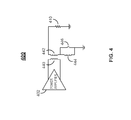
- FIG. 4 is an illustrative block diagram 400 of a multi-mode power amplification system, in accordance with an illustrative embodiment of the disclosure.
- Diagram 400 is similar to diagram 100 b with variable impedance load unit 112 as shown in diagram 200 a , except that an inductor 444 is used in place of capacitor 220 .
- Diagram 400 includes a power amplifier 402 , a pair of coupled inductors 440 and 442 , a resistor 410 , a third inductor 444 , and a switch 446 .
- power amplifier 402 may be adjustable and may correspond to the same adjustable power amplifier 102 as shown in FIGS. 1A and 1B .
- the coupled inductors 440 and 442 may correspond to a transformer (i.e., similar to balun 104 ), and the resistor 410 may correspond to the resistor 110 .
- the diagram 400 further includes a variable impedance unit (i.e., including inductor 444 and switch 446 ) coupled to an output terminal of the transformer (i.e., bottom terminal of inductor 442 ).
- the inductances of inductors 440 , 442 , and 444 may be the same or different. As an example, the inductance of inductor 440 may be 1 nH, and the inductances of inductors 442 and 444 may be 0.5 nH.
- the impedance of the variable impedance unit may be varied by opening and closing switch 446 .
- the switch 446 when the switch 446 is closed, inductor 444 is shorted out such that no current travels through inductor 444 .
- the impedance of the variable impedance unit is zero, such that the effective load impedance is determined by the resistance of resistor 410 and the transformation ratio of the transformer.
- switch 446 if switch 446 is open, current flows through inductor 444 , such that the impedance of the variable impedance unit corresponds to the impedance of inductor 444 .
- the effective load impedance is determined by the resistance of resistor 410 , the inductance of inductor 444 , and the transformation ratio of the transformer.
- the diagram 400 is another example of a multi-mode power amplifier that uses one or more inductors to vary the load impedance of the circuit.
- the diagram 400 is for illustrative purposes only, and one of ordinary skill in the art will understand that inductors and switches may be formed and added in parallel or in series appropriately in order to effectively vary the load impedance perceived by power amplifier 402 .
- any number of capacitors (such as capacitors 221 , 223 and 225 ), inductors (such as inductor 444 ), resistors (such as resistors 110 or 410 ), and/or switches (such as switches 220 , 222 , 224 , and 446 ) may be combined in any number of configurations (such as using parallel and/or series connections) in order to achieve a desirable value for an effective load impedance.
- FIGS. 5 and 6 include diagrams 500 and 600 of a circuit that may be used for a power amplifier 102 , in accordance with an illustrative embodiment of the present disclosure.
- the size of power amplifier 102 is adjustable such that different amounts of amplification are provided based on a desired mode of operation.
- the adjustable power amplifier 102 receives a signal from an input source and provides an amplified version of the signal to an output device such as balun 104 .
- Power amplifier 102 is configured to adjust its size (i.e., small or large) based on an aspect of the input signal.
- computing device 800 may be configured to adjust the size of power amplifier 102 .
- diagram 500 includes a load 550 , depicted here as a resistor outside of adjustable power amplifier 102 .
- Load 550 corresponds to the load impedance of the variable impedance unit 112 , which may or may not include a transformer such as balun 104 or a resistive load such as resistor 110 .
- load 550 may correspond to the impedance of everything shown in diagrams 100 a or 100 b except for power amplifier 102 .
- the impedance of load 550 may be dependent on the transformation ratio of a transformer such as balun 104 , the resistance of resistor 110 , and the overall impedance of variable impedance unit 112 .
- adjustable power amplifier 102 includes four transistors 552 , 554 , 556 and 558 , and a switch 560 .
- Transistors 552 - 558 may be NMOS transistors, each with a source terminal (i.e., the upper terminal), a gate terminal (i.e., the left terminal), and a drain terminal (i.e., the lower terminal).
- a transistor such as any of transistors 552 - 558 may have electrical conduction between the source and drain terminals depending on the voltage at the gate terminal. As an example, if the gate voltage at a transistor is within a certain range (i.e., when the gate voltage is low or below some threshold voltage), the transistor is “off”, such that no current flows between the source and drain terminals.
- Transistors 552 - 558 may have the same or different threshold voltages. As described herein, transistor 552 - 558 are three-terminal NMOS transistors. However, in general, transistors 552 - 558 may be any type of transistor, including PMOS transistors, CMOS transistors, BJT transistors, FET transistors, four terminal devices, or any combination thereof.
- transistors 552 and 554 are coupled such that the drain terminal of transistor 552 is coupled to the source terminal of transistor 554 .
- This configuration of transistors 552 and 554 may be a cascode amplifier, which is a two-stage amplifier.
- Transistors 556 and 558 have a similar configuration and may be a second cascode amplifier.
- the input port i.e., source terminal of transistor 552
- the output port i.e., drain terminal of transistor 554
- cascode amplifiers may be desirable when stability is a desirable feature.
- the cascode amplifier configuration offers several other advantages, including high gain, high bandwidth, and high input impedance.
- power amplifier 102 may adjust its size to be large or small.
- the two cascode amplifiers (a first cascode including transistors 552 and 554 , and a second cascode including transistors 556 and 558 ) are electrically coupled.
- the gate terminals of transistors 554 and 558 are coupled.
- switch 560 optionally couples the gate terminal of transistor 552 to the gate terminal of transistor 556 , or to ground.
- power amplifier 102 is a part of a wireless communication system that switches between using two standards (i.e., 802.11b and 802.11g).
- computing device 800 may adjust the size of power amplifier 102 be a “small” device (i.e., activate the first cascode amplifier and inactivate the second cascode amplifier).
- the input signal to the power amplifier may have a low peak to average ratio. Therefore, the power amplifier 102 only needs to be linear up to a limited extent, and a smaller amplifier is able to meet the linearity specification.
- switch 560 When a small device is desirable, switch 560 is coupled to ground, such that no current travels through transistors 556 and 558 and the second cascode amplifier is effectively off. In this case, only the first cascode amplifier is active, and the power amplifier of diagram 500 provides a smaller amount of amplification than if both cascode amplifiers (i.e., all four transistors) were active. By using only half the transistors in the device, power amplifier 102 consumes less power and is more efficient.
- computing device 800 may adjust the size of power amplifier 102 to be a “large” device (i.e., activate both cascode amplifiers) during operation in a second mode (i.e., 802.11g).
- the input signal to the power amplifier may have a high peak to average ratio. Therefore, the power amplifier 102 is required to be linear up to a higher extent, and a larger amplifier is necessary to meet the stricter linearity specification.
- switch 560 is coupled to the gate terminal of transistor 552 , such that transistors 552 and 556 have the same gate voltage.
- the second cascode amplifier is active (i.e., current flows through transistors 556 and 558 ) when the first cascode amplifier is active (i.e., current flows through transistors 552 and 554 ).
- the power amplifier of diagram 500 provides a large device that is able to meet the requirements associated with operation in the second mode. For example, operation in the second mode has a stricter linearity requirement, and additionally requires that the power amplifier 102 provide sufficient power. A small power amplifier 102 would be insufficient for use in the second mode because the small power amplifier would not be able to handle large peaks in the input signal (i.e., by becoming nonlinear or clipping the portions of the waveform with high amplitude). Thus, a large device is desirable for providing enough gain for signals with high peaks.
- the power amplifier 102 It is possible for the power amplifier 102 to keep both cascode amplifiers activated at all times, because a large device can handle input signals with both low and high peak to average ratios.
- activating both cascode amplifiers during operation in 802.11b mode is inefficient because a larger device consumes more power than a smaller device.
- use of a large device is wasteful when use of a smaller device would meet the requirements.
- switch 560 couples the gate terminal of transistor 556 to either the gate terminal of transistor 552 or ground.
- two switches may be used.
- a first switch may be used to couple the gate terminals of transistors 552 and 556
- a second switch may be used to couple the gate terminal of transistor 556 to ground.
- the first switch may be open and the second switch may be closed.
- the first switch may be closed and the second switch may be open when a large power amplifier is desirable.
- both switches may be closed (i.e., effectively grounding both gate terminals of transistors 552 and 556 ) if no power amplification is desired.
- Diagram 600 shows another example of an adjustable power amplifier 102 .
- Diagram 600 includes the same load 550 as shown in diagram 500 .
- Load 550 corresponds to the overall load impedance perceived by power amplifier 102 and may include a transformer such as balun 104 , resistor 110 , and/or a variable impedance unit 112 .
- adjustable power amplifier 102 includes two transistors 670 and 672 , two switches 674 and 676 , an input port 678 , and a bias port 680 .
- Each of transistors 670 and 672 may be considered as an amplifier portion of power amplifier 102 .
- transistor 672 may be activated or deactivated.
- switch 676 when switch 676 is closed and switch 674 is open (i.e., which may be controlled by computing device 800 ), the gate terminals of transistors 670 and 672 are coupled such that both transistors are activated.
- switch 676 when switch 676 is open and switch 674 is closed, transistor 672 is inactivated, effectively decreasing the size of power amplifier 102 by a factor of two.
- diagram 600 depicts input port 678 for receiving an input signal, which may cause current to flow through a capacitor and be added to current from a bias port 680 . The combined signal drives the gate terminal of transistor 670 at all times, and the gate terminal of transistor 672 when switch 676 is closed.
- adjustable power amplifier 102 is able to meet the requirements for a high amplitude signal, while being efficient signals with low amplitudes.
- Adjustable power amplifier 102 can have both amplifier portions (i.e., cascode amplifiers in diagram 500 and transistors 670 and 672 in diagram 600 ) activated for operation as a full-sized device, or can have a single amplifier portion activated for operation as a half-sized device.
- the size of the power amplifier 102 may be further adjusted (i.e., by opening and closing switches) for any suitable fraction of a full-sized device by coupling additional transistors and switches in parallel, in series, or in any other suitable configuration.
- transistors 552 - 558 in diagram 500 and transistors 670 - 672 in diagram 600 are shown for illustrative purposes only, and one of ordinary skill in the art will understand that any suitable configuration for adjustable power amplifier 102 may be used.
- any number of transistors may be coupled over any number of switches.
- adjustable power amplifier 102 may include any number of transistors or cascode amplifiers, coupled with switches such that the size of the power amplifier 102 may be appropriately adjusted for efficient operation in any number of modes.
- FIG. 7 shows a flow diagram of a process 700 for configuring parameters of a multi-mode power amplification system, in accordance with an embodiment of the disclosure.
- Process 700 is a high level illustration of a way that a computing device, such as computing device 800 described in relation to FIG. 8 , may configure a power amplification system for operation in different modes.
- process 700 includes configuring a size of an adjustable power amplifier 102 and configuring a desired load impedance of a variable impedance unit 112 , such that a single device may be used for efficient operation in multiple modes with different requirements and restrictions.
- Process 700 includes determining whether an input signal has a low peak to average ratio ( 702 ). If so, a small device is configured for power amplifier 102 ( 704 ) and a large load impedance is configured for variable impedance unit 112 ( 706 ). Otherwise, a large device is configured for power amplifier 102 ( 708 ) and a small load impedance is configured for variable impedance unit 112 ( 710 ).
- computing device 800 determines that an input signal has a low peak to average ratio at 702 , computing device 800 configures a small device for power amplifier 102 at 704 , and additionally configures a large load impedance for variable impedance unit 112 at 706 .
- computing device 800 may configure switches in power amplifier 102 such that half the power amplifier 102 becomes inactivated. For example, this may include grounding switch 560 in FIG. 5 or opening switch 676 and closing switch 674 in FIG. 6 .
- computing device 800 may configure switches in variable impedance unit 112 such that an effective load impedance is large. For example, this may include opening switch 106 in FIG. 1A or opening switch 220 in FIG. 2A .
- computing device 800 determines that an input signal does not have a low peak to average ratio at 702 , computing device 800 configures a large device for power amplifier 102 at 708 , and additionally configures a small load impedance for variable impedance unit 112 at 710 .
- computing device 800 may configure switches in power amplifier 102 such that the full device of power amplifier 102 becomes activated. For example, this may include coupling the gate terminals of transistors 552 and 556 in FIG. 5 or closing switch 676 and opening switch 674 in FIG. 6 .
- computing device 800 may configure switches in variable impedance unit 112 such that an effective load impedance is small. For example, this may include closing switch 106 in FIG. 1A or closing switch 220 in FIG. 2A .
- computing device 800 determines a mode of operation based on a peak to average ratio of the input signal. However, determination of an operation mode may be performed based on any aspect or feature of the input signal. Alternatively, determination of an operation mode may be based on another parameter not derived from the input signal, such as an operation mode of another system or a user input.
- Process 700 shows an illustrative flow diagram that uses a single predetermined threshold value for determining whether an input signal has a low peak to average ratio.
- the systems and methods described herein are applicable to any number of threshold values.
- the multi-modal power amplifier may be compatible with any number of modes, and selection of a mode may be dependent on whether the peak to average ratio of the input signal falls within some range of values.
- process 700 includes only two ranges of values, but the systems and methods described herein may be applied for any number of ranges for operation in multiple modes.
- FIG. 8 is a block diagram of a computing device 800 , such as any of the components of the systems of FIG. 1-2 or 4 - 6 , for performing any of the processes described herein.
- computing device 800 performing multi-modal power amplification
- any one or more portions of computing device 800 may be used alone to perform any of the processes described herein.
- system 100 a or 100 b may be coupled to CPU 806 , and it will be understood that CPU 806 may alone perform any of the processes described herein.
- Computing device 800 may be used to determine a desirable mode of operation, and configure the position of switches (i.e., opening or closing) based on the desired operational mode.
- switches i.e., opening or closing
- Each of the components of these systems may be implemented on one or more computing devices 800 .
- a plurality of the components of these systems may be included within one computing device 800 .
- a component and a storage device may be implemented across several computing devices 800 .
- the computing device 800 comprises at least one communications interface unit, an input/output controller 810 , system memory, and one or more data storage devices.
- the system memory includes at least one random access memory (RAM 802 ) and at least one read-only memory (ROM 804 ). All of these elements are in communication with a central processing unit (CPU 806 ) to facilitate the operation of the computing device 800 .
- the computing device 800 may be configured in many different ways. For example, the computing device 800 may be a conventional standalone computer or alternatively, the functions of computing device 800 may be distributed across multiple computer systems and architectures. In FIG. 8 , the computing device 800 is linked, via network or local network, to other servers or systems.
- the computing device 800 may be configured in a distributed architecture, wherein databases and processors are housed in separate units or locations. Some units perform primary processing functions and contain at a minimum a general controller or a processor and a system memory. In distributed architecture implementations, each of these units may be attached via the communications interface unit 808 to a communications hub or port (not shown) that serves as a primary communication link with other servers, client or user computers and other related devices.
- the communications hub or port may have minimal processing capability itself, serving primarily as a communications router.
- a variety of communications protocols may be part of the system, including, but not limited to: Ethernet, SAP, SASTM, ATP, BLUETOOTHTM, GSM and TCP/IP.
- the CPU 806 comprises a processor, such as one or more conventional microprocessors and one or more supplementary co-processors such as math co-processors for offloading workload from the CPU 806 .
- the CPU 806 is in communication with the communications interface unit 808 and the input/output controller 810 , through which the CPU 806 communicates with other devices such as other servers, user terminals, or devices.
- the communications interface unit 808 and the input/output controller 810 may include multiple communication channels for simultaneous communication with, for example, other processors, servers or client terminals.
- the CPU 806 is also in communication with the data storage device.
- the data storage device may comprise an appropriate combination of magnetic, optical or semiconductor memory, and may include, for example, RAM 802 , ROM 804 , flash drive, an optical disc such as a compact disc or a hard disk or drive.
- the CPU 806 and the data storage device each may be, for example, located entirely within a single computer or other computing device; or connected to each other by a communication medium, such as a USB port, serial port cable, a coaxial cable, an Ethernet cable, a telephone line, a radio frequency transceiver or other similar wireless or wired medium or combination of the foregoing.
- the CPU 806 may be connected to the data storage device via the communications interface unit 808 .
- the CPU 806 may be configured to perform one or more particular processing functions.
- the data storage device may store, for example, (i) an operating system 812 for the computing device 800 ; (ii) one or more applications 814 (e.g., computer program code or a computer program product) adapted to direct the CPU 806 in accordance with the systems and methods described here, and particularly in accordance with the processes described in detail with regard to the CPU 806 ; or (iii) database(s) 816 adapted to store information that may be utilized to store information required by the program.
- applications 814 e.g., computer program code or a computer program product
- the operating system 812 and applications 814 may be stored, for example, in a compressed, an uncompiled and an encrypted format, and may include computer program code.
- the instructions of the program may be read into a main memory of the processor from a computer-readable medium other than the data storage device, such as from the ROM 804 or from the RAM 802 . While execution of sequences of instructions in the program causes the CPU 806 to perform the process steps described herein, hard-wired circuitry may be used in place of, or in combination with, software instructions for implementation of the processes of the present disclosure. Thus, the systems and methods described are not limited to any specific combination of hardware and software.
- Suitable computer program code may be provided for performing one or more functions in relation to performing multi-modal power amplification as described herein.
- the program also may include program elements such as an operating system 812 , a database management system and “device drivers” that allow the processor to interface with computer peripheral devices (e.g., a video display, a keyboard, a computer mouse, etc.) via the input/output controller 810 .
- computer peripheral devices e.g., a video display, a keyboard, a computer mouse, etc.
- Non-volatile media include, for example, optical, magnetic, or opto-magnetic disks, or integrated circuit memory, such as flash memory.
- Volatile media include dynamic random access memory (DRAM), which typically constitutes the main memory.
- Computer-readable media include, for example, a floppy disk, a flexible disk, hard disk, magnetic tape, any other magnetic medium, a CD-ROM, DVD, any other optical medium, punch cards, paper tape, any other physical medium with patterns of holes, a RAM, a PROM, an EPROM or EEPROM (electronically erasable programmable read-only memory), a FLASH-EEPROM, any other memory chip or cartridge, or any other non-transitory medium from which a computer can read.
- a floppy disk a flexible disk, hard disk, magnetic tape, any other magnetic medium, a CD-ROM, DVD, any other optical medium, punch cards, paper tape, any other physical medium with patterns of holes, a RAM, a PROM, an EPROM or EEPROM (electronically erasable programmable read-only memory), a FLASH-EEPROM, any other memory chip or cartridge, or any other non-transitory medium from which a computer can read.
- Various forms of computer readable media may be involved in carrying one or more sequences of one or more instructions to the CPU 806 (or any other processor of a device described herein) for execution.
- the instructions may initially be borne on a magnetic disk of a remote computer (not shown).
- the remote computer can load the instructions into its dynamic memory and send the instructions over an Ethernet connection, cable line, or even telephone line using a modem.
- a communications device local to a computing device 800 e.g., a server
- the system bus carries the data to main memory, from which the processor retrieves and executes the instructions.
- the instructions received by main memory may optionally be stored in memory either before or after execution by the processor.
- instructions may be received via a communication port as electrical, electromagnetic or optical signals, which are exemplary forms of wireless communications or data streams that carry various types of information.
Abstract
Description
Claims (16)
Priority Applications (1)
| Application Number | Priority Date | Filing Date | Title |
|---|---|---|---|
| US13/660,755 US8957733B2 (en) | 2011-10-27 | 2012-10-25 | Systems and methods for performing multi-modal power amplification |
Applications Claiming Priority (2)
| Application Number | Priority Date | Filing Date | Title |
|---|---|---|---|
| US201161552410P | 2011-10-27 | 2011-10-27 | |
| US13/660,755 US8957733B2 (en) | 2011-10-27 | 2012-10-25 | Systems and methods for performing multi-modal power amplification |
Publications (2)
| Publication Number | Publication Date |
|---|---|
| US20130106507A1 US20130106507A1 (en) | 2013-05-02 |
| US8957733B2 true US8957733B2 (en) | 2015-02-17 |
Family
ID=47226418
Family Applications (1)
| Application Number | Title | Priority Date | Filing Date |
|---|---|---|---|
| US13/660,755 Active 2032-12-29 US8957733B2 (en) | 2011-10-27 | 2012-10-25 | Systems and methods for performing multi-modal power amplification |
Country Status (3)
| Country | Link |
|---|---|
| US (1) | US8957733B2 (en) |
| TW (1) | TWI578693B (en) |
| WO (1) | WO2013063212A1 (en) |
Cited By (1)
| Publication number | Priority date | Publication date | Assignee | Title |
|---|---|---|---|---|
| US9356560B2 (en) * | 2014-08-01 | 2016-05-31 | Qualcomm Incorporated | Multi-mode integrated power amplifier |
Families Citing this family (7)
| Publication number | Priority date | Publication date | Assignee | Title |
|---|---|---|---|---|
| EP2618481A1 (en) * | 2012-01-19 | 2013-07-24 | Nxp B.V. | Power amplifier circuit and control method |
| US9564860B2 (en) * | 2015-06-26 | 2017-02-07 | Acco | Multimode operation for differential power amplifiers |
| US10381991B1 (en) * | 2018-02-02 | 2019-08-13 | Psemi Corporation | Drain sharing split LNA |
| US10903544B2 (en) | 2019-04-25 | 2021-01-26 | International Business Machines Corporation | Magnetic balun/transformer with post processing adjustments |
| EP3829068A1 (en) | 2019-11-29 | 2021-06-02 | Socionext Inc. | Transformer circuitry |
| US20230020495A1 (en) * | 2021-07-13 | 2023-01-19 | Skyworks Solutions, Inc. | Load-modulated push-pull power amplifier |
| US11539382B1 (en) | 2021-10-19 | 2022-12-27 | Psemi Corporation | Supporting wideband inputs on RF receivers |
Citations (17)
| Publication number | Priority date | Publication date | Assignee | Title |
|---|---|---|---|---|
| US6255906B1 (en) | 1999-09-30 | 2001-07-03 | Conexant Systems, Inc. | Power amplifier operated as an envelope digital to analog converter with digital pre-distortion |
| US6301467B1 (en) | 1997-06-02 | 2001-10-09 | Nokia Mobile Phones Ltd. | Bias voltage controlled parallel active components |
| US6349216B1 (en) * | 1999-07-22 | 2002-02-19 | Motorola, Inc. | Load envelope following amplifier system |
| US6556814B1 (en) * | 1999-07-22 | 2003-04-29 | Motorola, Inc. | Memory-based amplifier load adjust system |
| US20040075494A1 (en) | 2002-10-17 | 2004-04-22 | Armin Klomsdorf | Power amplification circuit and method for supplying power at a plurality of desired power output levels |
| US20050030094A1 (en) | 2003-08-05 | 2005-02-10 | Motorola, Inc. | Low power consumption adaptive power amplifier |
| US20050206457A1 (en) * | 2004-03-17 | 2005-09-22 | James Martin | Amplifier system and method |
| US20060132232A1 (en) | 2004-12-17 | 2006-06-22 | Atiqul Baree | Multi-mode power amplifier |
| US20060178121A1 (en) | 2003-02-25 | 2006-08-10 | Miikka Hamalainen | Method and a device for adjusting power amplifier properties |
| US7113033B2 (en) | 2002-01-31 | 2006-09-26 | Qualcomm Incorporated | Variable impedance load for a variable gain radio frequency amplifier |
| US20110025415A1 (en) | 2009-08-03 | 2011-02-03 | Fenghao Mu | Digital Modulated RF Power Amplifier with Impedance Compensation Circuit |
| US20110070848A1 (en) | 2009-09-21 | 2011-03-24 | Broadcom Corporation | Dynamic stability, gain, efficiency and impedance control in a linear/non-linear CMOS power amplifier |
| US7944296B1 (en) | 2010-03-12 | 2011-05-17 | Samsung Electro-Mechanics Company | Low power mode amplification with a transformer output matching and a virtual ground |
| US7982543B1 (en) | 2009-03-30 | 2011-07-19 | Triquint Semiconductor, Inc. | Switchable power amplifier |
| US20110187451A1 (en) | 2010-02-03 | 2011-08-04 | Samsung Electro-Mechanics Co., Ltd. | Power amplifier |
| US7994296B2 (en) | 2002-03-27 | 2011-08-09 | Perkinelmer Health Sciences, Inc. | Arrays, computer program products and methods for in silico array-based comparative binding assays |
| US8466749B2 (en) * | 2010-11-01 | 2013-06-18 | Fujitsu Semiconductor Limited | Variable gain amplifier |
Family Cites Families (9)
| Publication number | Priority date | Publication date | Assignee | Title |
|---|---|---|---|---|
| US5673001A (en) * | 1995-06-07 | 1997-09-30 | Motorola, Inc. | Method and apparatus for amplifying a signal |
| KR100676354B1 (en) * | 2000-03-02 | 2007-01-31 | 산요덴키가부시키가이샤 | Variable resistance circuit, operational amplification circuit, semiconductor integrated circuit, time constant switching circuit and waveform shaping circuit |
| GB0407663D0 (en) * | 2004-04-03 | 2004-05-05 | Ibm | Variable gain amplifier |
| TW200836474A (en) * | 2007-02-27 | 2008-09-01 | Advanced Analog Technology Inc | Power transistor circuit with high-voltage endurance and method thereof |
| US7911277B2 (en) * | 2007-10-16 | 2011-03-22 | Black Sand Technologies, Inc. | Adaptively tuned RF power amplifier |
| US7679402B2 (en) * | 2008-04-03 | 2010-03-16 | International Business Machines Corporation | Methods and apparatus for monitoring power gating circuitry and for controlling circuit operations in dependence on monitored power gating conditions |
| JP5321126B2 (en) * | 2009-02-24 | 2013-10-23 | 富士通セミコンダクター株式会社 | Analog switch circuit |
| US7786807B1 (en) * | 2009-04-23 | 2010-08-31 | Broadcom Corporation | Cascode CMOS RF power amplifier with programmable feedback cascode bias under multiple supply voltages |
| TWI415387B (en) * | 2009-07-22 | 2013-11-11 | Amazing Microelectronic Corp | An improved power amplifier and a method for restraining power of the improved power amplifier |
-
2012
- 2012-10-25 WO PCT/US2012/061831 patent/WO2013063212A1/en active Application Filing
- 2012-10-25 US US13/660,755 patent/US8957733B2/en active Active
- 2012-10-26 TW TW101139795A patent/TWI578693B/en not_active IP Right Cessation
Patent Citations (18)
| Publication number | Priority date | Publication date | Assignee | Title |
|---|---|---|---|---|
| US6301467B1 (en) | 1997-06-02 | 2001-10-09 | Nokia Mobile Phones Ltd. | Bias voltage controlled parallel active components |
| US6349216B1 (en) * | 1999-07-22 | 2002-02-19 | Motorola, Inc. | Load envelope following amplifier system |
| US6556814B1 (en) * | 1999-07-22 | 2003-04-29 | Motorola, Inc. | Memory-based amplifier load adjust system |
| US20030199256A1 (en) | 1999-07-22 | 2003-10-23 | Armin Klomsdorf | Memory-based amplifier load adjust system |
| US6255906B1 (en) | 1999-09-30 | 2001-07-03 | Conexant Systems, Inc. | Power amplifier operated as an envelope digital to analog converter with digital pre-distortion |
| US7113033B2 (en) | 2002-01-31 | 2006-09-26 | Qualcomm Incorporated | Variable impedance load for a variable gain radio frequency amplifier |
| US7994296B2 (en) | 2002-03-27 | 2011-08-09 | Perkinelmer Health Sciences, Inc. | Arrays, computer program products and methods for in silico array-based comparative binding assays |
| US20040075494A1 (en) | 2002-10-17 | 2004-04-22 | Armin Klomsdorf | Power amplification circuit and method for supplying power at a plurality of desired power output levels |
| US20060178121A1 (en) | 2003-02-25 | 2006-08-10 | Miikka Hamalainen | Method and a device for adjusting power amplifier properties |
| US20050030094A1 (en) | 2003-08-05 | 2005-02-10 | Motorola, Inc. | Low power consumption adaptive power amplifier |
| US20050206457A1 (en) * | 2004-03-17 | 2005-09-22 | James Martin | Amplifier system and method |
| US20060132232A1 (en) | 2004-12-17 | 2006-06-22 | Atiqul Baree | Multi-mode power amplifier |
| US7982543B1 (en) | 2009-03-30 | 2011-07-19 | Triquint Semiconductor, Inc. | Switchable power amplifier |
| US20110025415A1 (en) | 2009-08-03 | 2011-02-03 | Fenghao Mu | Digital Modulated RF Power Amplifier with Impedance Compensation Circuit |
| US20110070848A1 (en) | 2009-09-21 | 2011-03-24 | Broadcom Corporation | Dynamic stability, gain, efficiency and impedance control in a linear/non-linear CMOS power amplifier |
| US20110187451A1 (en) | 2010-02-03 | 2011-08-04 | Samsung Electro-Mechanics Co., Ltd. | Power amplifier |
| US7944296B1 (en) | 2010-03-12 | 2011-05-17 | Samsung Electro-Mechanics Company | Low power mode amplification with a transformer output matching and a virtual ground |
| US8466749B2 (en) * | 2010-11-01 | 2013-06-18 | Fujitsu Semiconductor Limited | Variable gain amplifier |
Non-Patent Citations (1)
| Title |
|---|
| International Search Report and Written Report dated Mar. 21, 2013 in International Application No. PCT/US2012/061831. |
Cited By (1)
| Publication number | Priority date | Publication date | Assignee | Title |
|---|---|---|---|---|
| US9356560B2 (en) * | 2014-08-01 | 2016-05-31 | Qualcomm Incorporated | Multi-mode integrated power amplifier |
Also Published As
| Publication number | Publication date |
|---|---|
| WO2013063212A1 (en) | 2013-05-02 |
| TWI578693B (en) | 2017-04-11 |
| US20130106507A1 (en) | 2013-05-02 |
| TW201320585A (en) | 2013-05-16 |
Similar Documents
| Publication | Publication Date | Title |
|---|---|---|
| US8957733B2 (en) | Systems and methods for performing multi-modal power amplification | |
| US20230075284A1 (en) | Systems and Methods for Optimizing Amplifier Operations | |
| JP6149452B2 (en) | Power supply device and semiconductor integrated circuit device | |
| EP3264597B1 (en) | Doherty amplifier circuits | |
| JP6332842B2 (en) | Electronic circuits having variable attenuators and methods of their operation | |
| US9088248B2 (en) | Amplifier and mobile communication device | |
| KR101113492B1 (en) | Hige power tunable capacitor | |
| US11201595B2 (en) | Cascode power amplifier with switchable output matching network | |
| EP2946467B1 (en) | Amplifier with switchable common gate gain buffer | |
| US10171048B2 (en) | Power amplifier | |
| CN104871429B (en) | Tunable broad band exciting amplifier | |
| CN110268626A (en) | The bias modulation active linear of broad band amplifier | |
| CN102195569A (en) | Systems and methods for positive and negative feedback of cascode transistors for a power amplifier | |
| KR20230011248A (en) | Load-modulated push-pull power amplifier | |
| US9438180B2 (en) | Radio frequency power amplifier and method for increasing power added efficiency and linearity | |
| JP6532146B2 (en) | Switch mode amplifier | |
| US20150171800A1 (en) | Tunable loadline | |
| US20130082779A1 (en) | Amplifier | |
| US9160309B2 (en) | Area efficient baseband filter | |
| EP3367564B1 (en) | Linear amplifier having higher efficiency for envelope tracking modulator | |
| US7944304B1 (en) | High efficiency millimeter wave field-effect transistor (FET) amplifier with coupled line matching network | |
| CN110995175A (en) | Amplifier and amplifying method | |
| US11552601B2 (en) | Power amplifier circuit | |
| US11190165B1 (en) | Wideband low power active isolator | |
| Allam-Ouyahia et al. | Bandwidth enhancement of an inverse class-F power amplifier based on LDMOS devices |
Legal Events
| Date | Code | Title | Description |
|---|---|---|---|
| AS | Assignment |
Owner name: MARVELL INTERNATIONAL LTD., BERMUDA Free format text: LICENSE;ASSIGNOR:MARVELL WORLD TRADE LTD.;REEL/FRAME:029262/0285 Effective date: 20121106 Owner name: MARVELL INTERNATIONAL LTD., BERMUDA Free format text: ASSIGNMENT OF ASSIGNORS INTEREST;ASSIGNOR:MARVELL SEMICONDUCTOR, INC.;REEL/FRAME:029262/0026 Effective date: 20121024 Owner name: MARVELL SEMICONDUCTOR, INC., CALIFORNIA Free format text: ASSIGNMENT OF ASSIGNORS INTEREST;ASSIGNORS:SIGNOFF, DAVID M.;LIAO, SHU-HSIEN;HE, MING;AND OTHERS;SIGNING DATES FROM 20121011 TO 20121023;REEL/FRAME:029261/0976 Owner name: MARVELL WORLD TRADE LTD., BARBADOS Free format text: ASSIGNMENT OF ASSIGNORS INTEREST;ASSIGNOR:MARVELL INTERNATIONAL LTD.;REEL/FRAME:029262/0089 Effective date: 20121024 |
|
| STCF | Information on status: patent grant |
Free format text: PATENTED CASE |
|
| MAFP | Maintenance fee payment |
Free format text: PAYMENT OF MAINTENANCE FEE, 4TH YEAR, LARGE ENTITY (ORIGINAL EVENT CODE: M1551) Year of fee payment: 4 |
|
| AS | Assignment |
Owner name: MARVELL INTERNATIONAL LTD., BERMUDA Free format text: ASSIGNMENT OF ASSIGNORS INTEREST;ASSIGNOR:MARVELL WORLD TRADE LTD.;REEL/FRAME:051778/0537 Effective date: 20191231 |
|
| AS | Assignment |
Owner name: CAVIUM INTERNATIONAL, CAYMAN ISLANDS Free format text: ASSIGNMENT OF ASSIGNORS INTEREST;ASSIGNOR:MARVELL INTERNATIONAL LTD.;REEL/FRAME:052918/0001 Effective date: 20191231 |
|
| AS | Assignment |
Owner name: MARVELL ASIA PTE, LTD., SINGAPORE Free format text: ASSIGNMENT OF ASSIGNORS INTEREST;ASSIGNOR:CAVIUM INTERNATIONAL;REEL/FRAME:053475/0001 Effective date: 20191231 |
|
| MAFP | Maintenance fee payment |
Free format text: PAYMENT OF MAINTENANCE FEE, 8TH YEAR, LARGE ENTITY (ORIGINAL EVENT CODE: M1552); ENTITY STATUS OF PATENT OWNER: LARGE ENTITY Year of fee payment: 8 |