US8952950B2 - Display apparatus and apparatus and method for generating power voltages - Google Patents
Display apparatus and apparatus and method for generating power voltages Download PDFInfo
- Publication number
- US8952950B2 US8952950B2 US12/659,613 US65961310A US8952950B2 US 8952950 B2 US8952950 B2 US 8952950B2 US 65961310 A US65961310 A US 65961310A US 8952950 B2 US8952950 B2 US 8952950B2
- Authority
- US
- United States
- Prior art keywords
- power voltage
- voltage
- storage capacitor
- gamma
- power
- Prior art date
- Legal status (The legal status is an assumption and is not a legal conclusion. Google has not performed a legal analysis and makes no representation as to the accuracy of the status listed.)
- Expired - Fee Related, expires
Links
Images


Classifications
-
- G—PHYSICS
- G09—EDUCATION; CRYPTOGRAPHY; DISPLAY; ADVERTISING; SEALS
- G09G—ARRANGEMENTS OR CIRCUITS FOR CONTROL OF INDICATING DEVICES USING STATIC MEANS TO PRESENT VARIABLE INFORMATION
- G09G3/00—Control arrangements or circuits, of interest only in connection with visual indicators other than cathode-ray tubes
- G09G3/20—Control arrangements or circuits, of interest only in connection with visual indicators other than cathode-ray tubes for presentation of an assembly of a number of characters, e.g. a page, by composing the assembly by combination of individual elements arranged in a matrix no fixed position being assigned to or needed to be assigned to the individual characters or partial characters
- G09G3/22—Control arrangements or circuits, of interest only in connection with visual indicators other than cathode-ray tubes for presentation of an assembly of a number of characters, e.g. a page, by composing the assembly by combination of individual elements arranged in a matrix no fixed position being assigned to or needed to be assigned to the individual characters or partial characters using controlled light sources
- G09G3/30—Control arrangements or circuits, of interest only in connection with visual indicators other than cathode-ray tubes for presentation of an assembly of a number of characters, e.g. a page, by composing the assembly by combination of individual elements arranged in a matrix no fixed position being assigned to or needed to be assigned to the individual characters or partial characters using controlled light sources using electroluminescent panels
- G09G3/32—Control arrangements or circuits, of interest only in connection with visual indicators other than cathode-ray tubes for presentation of an assembly of a number of characters, e.g. a page, by composing the assembly by combination of individual elements arranged in a matrix no fixed position being assigned to or needed to be assigned to the individual characters or partial characters using controlled light sources using electroluminescent panels semiconductive, e.g. using light-emitting diodes [LED]
- G09G3/3208—Control arrangements or circuits, of interest only in connection with visual indicators other than cathode-ray tubes for presentation of an assembly of a number of characters, e.g. a page, by composing the assembly by combination of individual elements arranged in a matrix no fixed position being assigned to or needed to be assigned to the individual characters or partial characters using controlled light sources using electroluminescent panels semiconductive, e.g. using light-emitting diodes [LED] organic, e.g. using organic light-emitting diodes [OLED]
- G09G3/3275—Details of drivers for data electrodes
- G09G3/3291—Details of drivers for data electrodes in which the data driver supplies a variable data voltage for setting the current through, or the voltage across, the light-emitting elements
-
- G—PHYSICS
- G09—EDUCATION; CRYPTOGRAPHY; DISPLAY; ADVERTISING; SEALS
- G09G—ARRANGEMENTS OR CIRCUITS FOR CONTROL OF INDICATING DEVICES USING STATIC MEANS TO PRESENT VARIABLE INFORMATION
- G09G3/00—Control arrangements or circuits, of interest only in connection with visual indicators other than cathode-ray tubes
- G09G3/20—Control arrangements or circuits, of interest only in connection with visual indicators other than cathode-ray tubes for presentation of an assembly of a number of characters, e.g. a page, by composing the assembly by combination of individual elements arranged in a matrix no fixed position being assigned to or needed to be assigned to the individual characters or partial characters
-
- G—PHYSICS
- G09—EDUCATION; CRYPTOGRAPHY; DISPLAY; ADVERTISING; SEALS
- G09G—ARRANGEMENTS OR CIRCUITS FOR CONTROL OF INDICATING DEVICES USING STATIC MEANS TO PRESENT VARIABLE INFORMATION
- G09G2310/00—Command of the display device
- G09G2310/02—Addressing, scanning or driving the display screen or processing steps related thereto
- G09G2310/0264—Details of driving circuits
- G09G2310/027—Details of drivers for data electrodes, the drivers handling digital grey scale data, e.g. use of D/A converters
-
- G—PHYSICS
- G09—EDUCATION; CRYPTOGRAPHY; DISPLAY; ADVERTISING; SEALS
- G09G—ARRANGEMENTS OR CIRCUITS FOR CONTROL OF INDICATING DEVICES USING STATIC MEANS TO PRESENT VARIABLE INFORMATION
- G09G2320/00—Control of display operating conditions
- G09G2320/06—Adjustment of display parameters
- G09G2320/0673—Adjustment of display parameters for control of gamma adjustment, e.g. selecting another gamma curve
-
- G—PHYSICS
- G09—EDUCATION; CRYPTOGRAPHY; DISPLAY; ADVERTISING; SEALS
- G09G—ARRANGEMENTS OR CIRCUITS FOR CONTROL OF INDICATING DEVICES USING STATIC MEANS TO PRESENT VARIABLE INFORMATION
- G09G2330/00—Aspects of power supply; Aspects of display protection and defect management
- G09G2330/02—Details of power systems and of start or stop of display operation
- G09G2330/028—Generation of voltages supplied to electrode drivers in a matrix display other than LCD
-
- G—PHYSICS
- G09—EDUCATION; CRYPTOGRAPHY; DISPLAY; ADVERTISING; SEALS
- G09G—ARRANGEMENTS OR CIRCUITS FOR CONTROL OF INDICATING DEVICES USING STATIC MEANS TO PRESENT VARIABLE INFORMATION
- G09G2330/00—Aspects of power supply; Aspects of display protection and defect management
- G09G2330/06—Handling electromagnetic interferences [EMI], covering emitted as well as received electromagnetic radiation
Definitions
- the embodiments relate to a display apparatus, an apparatus for generating power voltages, and a method thereof, and more particularly, to a display apparatus generating a storage capacitor power voltage and a gamma filter power voltage from a voltage supplied by a voltage source, an apparatus for generating a storage capacitor power voltage and a gamma filter power voltage from a voltage supplied by a voltage source, and a method thereof.
- a display apparatus including a plurality of pixels controls brightness of each of the pixels by applying a data driving signal corresponding to input data to each of the pixels.
- the display apparatus converts the input data into an image, and displays the image to a user.
- the data driving signals to be output to the plurality of pixels are generated by a data driving unit.
- the data driving unit selects a gamma voltage corresponding to the input data from a plurality of gamma voltages.
- the gamma voltages are generated by a gamma filter circuit.
- the data driving unit outputs the selected gamma voltage to a plurality of pixel circuits as the data driving signal.
- Embodiments are therefore directed to a display apparatus generating a storage capacitor power voltage and a gamma filter power voltage from a voltage supplied by a voltage source, an apparatus for generating a storage capacitor power voltage and a gamma filter power voltage from a voltage supplied by a voltage source, and a method thereof, which substantially overcome one or more of the problems due to the limitations and disadvantages of the related art.
- a display apparatus comprising: a plurality of pixel circuits including a storage capacitor that stores a voltage potential of a data driving signal; a data driving unit including a gamma voltage generating unit configured to generate a plurality of gamma voltages, data driving unit configured to generate a plurality of data driving signals from the plurality of gamma voltages, and output the plurality of data driving signals to the plurality of pixel circuits; a scan driving unit configured to generate a plurality of scan signals and output the plurality of scan signals to the plurality of pixel circuits; and a power voltage generating unit configured to generate a gamma filter power voltage and a storage capacitor power voltage using a first power voltage, apply the gamma filter power voltage to the gamma voltage generating unit, and apply the storage capacitor power voltage to the storage capacitors included in the plurality of pixels, wherein the first power voltage is generated from a power voltage supplied by a voltage source, and the gamma
- the power voltage generating unit may comprise: a storage capacitor power outputting unit configured to generate the storage capacitor power voltage and output the storage capacitor power voltage; and a gamma filter power outputting unit configured to generate the gamma filter power voltage and output the gamma filter power voltage.
- the power voltage generating unit may further comprise a voltage dividing unit configured to generate a second power voltage and a third power voltage from the first power voltage, output the second power voltage to the storage capacitor power outputting unit, and output the third power voltage to the gamma filter power outputting unit, wherein the storage capacitor power outputting unit may generate the storage capacitor power voltage from the second power voltage, wherein the gamma filter power outputting unit may generate the gamma filter power voltage from the third power voltage, and wherein the second power voltage and the third power voltage may have the same phase.
- the voltage dividing unit may include a first resistor and a second resistor, the first and second resistors may be coupled in series, one end of the first resistor may be coupled to an input of the storage capacitor power outputting unit, and the other end of the first resistor and one end of the second resistor may be coupled to an input of the gamma filter power outputting unit.
- the gamma filter power outputting unit may generate a fourth power voltage from the storage capacitor power voltage and generate the gamma filter power voltage from the fourth power voltage, and the fourth voltage and the storage capacitor power voltage may have the same phase.
- the gamma filter power outputting unit may include a third resistor and a fourth resistor, the third and fourth resistors may be coupled in series, and one end of the third resistor may be coupled to an output of the storage capacitor power outputting unit.
- the display apparatus may be an organic light emitting diode (OLED) display apparatus.
- OLED organic light emitting diode
- the power voltage generating unit may comprise a reference voltage outputting unit configured to generate the first power voltage from the power voltage supplied by a voltage source, and output the first power voltage.
- the first power voltage generated may be divided so as to generate the storage capacitor power voltage and the gamma filter power voltage.
- the gamma voltage generating unit may divide the gamma filter power voltage into the plurality of gamma voltages so that the plurality of gamma voltages and the storage capacitor power voltage have the same phase.
- an apparatus for generating power voltages of a display apparatus including a plurality of pixel circuits comprising: a storage capacitor power outputting unit configured to generate a storage capacitor power voltage using a first power voltage and apply the storage capacitor power voltage to storage capacitors, each included in each of the plurality of pixel circuits; and a gamma filter power outputting unit configured to generate a gamma filter power voltage using the first power voltage and apply the gamma filter power voltage to a gamma voltage generating unit, wherein the first power voltage is generated from a power voltage supplied by a voltage source, and the storage capacitor power voltage and the gamma filter power voltage have the same phase.
- the apparatus may further comprise a voltage dividing unit configured to generate a second power voltage and a third power voltage from the first power voltage, output the second power voltage to the storage capacitor power outputting unit, and output the third power voltage to the gamma filter power outputting unit, wherein the storage capacitor power outputting unit may generate the storage capacitor power voltage from the second power voltage, wherein the gamma filter power outputting unit may generate the gamma filter power voltage from the third power voltage, and wherein the second power voltage and the third power voltage may have the same phase.
- a voltage dividing unit configured to generate a second power voltage and a third power voltage from the first power voltage, output the second power voltage to the storage capacitor power outputting unit, and output the third power voltage to the gamma filter power outputting unit, wherein the storage capacitor power outputting unit may generate the storage capacitor power voltage from the second power voltage, wherein the gamma filter power outputting unit may generate the gamma filter power voltage from the third power voltage, and wherein the second power voltage and the third power voltage may
- the voltage dividing unit may include a first resistor and a second resistor, the first and second resistors may be coupled in series, one end of the first resistor may be coupled to an input of the storage capacitor power outputting unit, and the other end of the first resistor and one end of the second resistor may be coupled to an input of the gamma filter power outputting unit.
- the gamma filter power outputting unit may generate a fourth power voltage from the storage capacitor power voltage and generate the gamma filter power voltage from the fourth power voltage, and the fourth voltage and the storage capacitor power voltage may have the same phase.
- the gamma filter power outputting unit may include a third resistor and a fourth resistor, the third and fourth resistors may be coupled in series, and one end of the third resistor may be coupled to an output of the storage capacitor power outputting unit.
- the display apparatus may be an OLED display apparatus.
- the power voltage generating unit may comprise a reference voltage outputting unit configured to generate the first power voltage from the power voltage supplied by a voltage source, and output the first power voltage.
- the first power voltage may be divided so as to generate the storage capacitor power voltage and the gamma filter power voltage.
- FIG. 1 illustrates a schematic block diagram of a display apparatus according to an embodiment
- FIG. 2 illustrates a schematic circuit diagram of a power voltage generating unit according to an embodiment
- FIG. 3 illustrates a schematic circuit diagram of a power voltage generating unit according to another embodiment
- FIG. 4A illustrates a diagram for explaining a mechanism of cancelling/reducing noise associated with an external power voltage or a first power voltage according to the embodiments
- FIG. 4B illustrates waveforms of a storage capacitor power voltage and a gamma filter power voltage for explaining the mechanism of cancelling/reducing noise associated with the external power voltage or the first power voltage according to the embodiments;
- FIG. 5 illustrates a schematic circuit diagram of a data driving unit according to an embodiment
- FIG. 6 illustrates a schematic circuit of a gamma voltage generating unit according to an embodiment
- FIG. 7 illustrates a schematic configuration of a plurality of pixel circuits according to an embodiment
- FIG. 8 illustrates a schematic circuit of a pixel circuit according to an embodiment
- FIG. 9 is a flowchart illustrating a method for generating power voltages to be supplied to a display apparatus according to an embodiment.
- FIG. 1 illustrates a schematic block diagram of a display apparatus 100 according to an embodiment.
- the display apparatus 100 may include a timing control unit 110 , a data driving unit 120 , a scan driving unit 130 , a plurality of pixel circuits 140 , and a power voltage generating unit 150 .
- the timing control unit 110 may receive a vertical synchronization (sync) signal Vsync, a horizontal sync signal Hsync, a data enable signal DE, and an image data signal DATA_in.
- the timing control unit 110 may convert the image data signal DATA_in to a RGB data signal DATA, and output the RGB data signal DATA to the data driving unit 120 according to the requirements of the data driving unit 120 .
- the timing control unit 110 may also generate a start horizontal signal STH and a load signal TP, and may output the signals STH and TP to the data driving unit 120 .
- the signals STH and TP may be used to provide a reference time period for which data driving signals D 1 , D 2 , . . . , D M are output to the pixel circuits 140 from the data driving unit 120 .
- the timing control unit 110 may output a start vertical signal STV, a gate clock signal CPV, and an output enable signal OE to the scan driving unit 130 .
- the start vertical signal STV may be used for selecting a first scan line.
- the gate clock signal CPV may be used for sequentially selecting the next gate line.
- the output enable signal OE may be used for controlling an output of the scan driving unit 130 .
- the data driving unit 120 may include a plurality of data driver integrated circuits (ICs).
- the data driving unit 120 may receive the RGB data signal DATA and the signals STH and TP, which are input from the timing control unit 110 .
- the data driving unit 120 may generate the data driving signals D 1 , D 2 , . . . , D M , and output each of the data driving signals D 1 , D 2 , . . . , D M to each data line.
- the data driving signals D 1 , D 2 , . . . , D M may be applied to the pixel circuits 140 .
- the data driving unit 120 may include a gamma voltage generating unit 122 .
- the gamma voltage generating unit 122 may divide a gamma filter power voltage Vgamma into a plurality of gamma voltages.
- the scan driving unit 130 may include a plurality of scan driver ICs.
- the scan driving unit 130 may apply each of a plurality of scan signals S 1 , S 2 , . . . , S N to each of the scan lines connected to the pixel circuits 140 according to the signals CPV, STV, and OE provided by the timing control unit 110 .
- the scan driving unit 130 may sequentially scan the pixel circuits 140 per pixel circuits connected to each scan line. For example, pixel circuits 140 arranged in the same row may be connected to the same scan line. In this case, the pixel circuits 140 may be sequentially scanned per pixel circuits connected to each scan line.
- the pixel circuits 140 may be driven according to the scan signals S 1 , S 2 , . . . , S N and the data driving signals D 1 , D 2 , . . . , D M .
- the pixel circuits 140 may emit light according to the driving signals D 1 , D 2 , . . . , D M .
- the pixel circuits 140 may be arranged in the form of a two dimensional matrix such as an M ⁇ N matrix (M and N are natural numbers). Also, the pixel circuits 140 may emit light by using, for example, organic light emitting diodes (OLEDs).
- An anode power voltage ELVDD and a cathode power voltage ELVSS may be applied to each of the pixel circuits 140 to drive each of the pixel circuits 140 .
- Each of the pixel circuits 140 may include a storage capacitor Cst used to store voltage potentials of the driving signals D 1 , D 2 , . . . , D M .
- the storage capacitor Cst may use a power voltage other than the anode power voltage ELVDD and the cathode power voltage ELVSS.
- a power voltage connected to the storage capacitor Cst is referred to as a storage capacitor power voltage.
- the storage capacitor power voltage may be the same as the anode power voltage ELVDD. However, embodiments are not limited thereto.
- the storage capacitor power voltage may be different from the anode power voltage ELVDD.
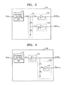
- FIG. 2 illustrates a schematic circuit diagram of a power voltage generating unit 150 a according to an embodiment.
- the power voltage generating unit 150 a may divide a first power voltage Vref 1 so as to produce a gamma filter power voltage Vgamma and a storage capacitor power voltage ELVDD.
- the power voltage generating unit 150 a may include a reference voltage outputting unit 210 , a voltage dividing unit 220 , a storage capacitor power outputting unit 230 , and a gamma filter power outputting unit 240 a.
- the reference voltage outputting unit 210 may receive an external power voltage Vsource from an external voltage source (not shown), and generate the first power voltage Vref 1 .
- the reference voltage outputting unit 210 may adjust a voltage potential of the first power voltage Vref 1 for the process of reducing/cancelling noise associated with the external power voltage Vsource.
- the voltage dividing unit 220 may divide the first power voltage Vref 1 so as to produce a second power voltage Vref 2 and a third power voltage Vref 3 .
- the voltage dividing unit 220 may adjust resistances of resistors R 1 and R 2 , and produce desired potentials of the second power voltage Vref 2 and the third power voltage Vref 3 , respectively.
- the storage capacitor power outputting unit 230 may amplify the second power voltage Vref 2 , and output the storage capacitor power voltage ELVDD to the pixel circuits 140 .
- the gamma filter power outputting unit 240 a may amplify the third power voltage Vref 3 , and output the gamma filter power voltage Vgamma to the pixel circuits 140 .
- the storage capacitor power outputting unit 230 and the gamma filter power outputting unit 240 a may be implemented using an operational amplifier (op-amp) that is a source follower.
- op-amp operational amplifier
- FIG. 3 illustrates a schematic circuit diagram of a power voltage generating unit 150 b according to another embodiment.
- the power voltage generating unit 150 b may include the reference voltage outputting unit 210 , the storage capacitor power outputting unit 230 , and a gamma filter power outputting unit 240 b.
- the storage capacitor power outputting unit 230 may amplify the first power voltage Vref 1 generated by the reference voltage outputting unit 210 , and output the storage capacitor power voltage ELVDD to the pixel circuits 140 .
- the gamma filter power outputting unit 240 b may divide the storage capacitor power voltage ELVDD output from the storage capacitor power outputting unit 230 and obtain the divided storage capacitor power voltage, that is, a fourth power voltage Vref 4 .
- the gamma filter power outputting unit 240 b may amplify the fourth power voltage Vref 4 , and output the gamma filter power voltage Vgamma.
- the gamma filter power outputting unit 240 b may include resistors R 1 and R 2 . Resistances of the resistors R 1 and R 2 may be adjusted to obtain a desired potential of the gamma filter power voltage Vgamma.
- the gamma filter power outputting unit 240 b may include a source follower 242 used to amplify the fourth power voltage Vref 4 .
- FIG. 4A illustrates a diagram for explaining a mechanism of cancelling/reducing noise associated with the external power voltage Vsource or the first power voltage Vref 1 according to the embodiments.
- a power voltage noise having a pattern A may be included in the first power voltage Vref 1 generated by the reference voltage outputting unit 210 . Since both the storage capacitor power voltage ELVDD and the gamma filter power voltage Vgamma are generated from the first power voltage Vref 1 , the storage capacitor power voltage ELVDD and the gamma filter power voltage Vgamma may have noise having the same pattern A. More specifically, resistors may be used to divide the first power voltage Vref 1 so as to produce the storage capacitor power voltage ELVDD and the gamma filter power voltage Vgamma. Therefore, the storage capacitor power voltage ELVDD and the gamma filter power voltage Vgamma may have noise having the same phase.
- the respective data driving signals D 1 , D 2 , . . . , D M that are generated from the gamma filter power voltage Vgamma may be applied to one end of the storage capacitor Cst included in each pixel circuit, while the storage capacitor power voltage ELVDD may be applied to the other end of the storage capacitor Cst included in each pixel circuit. Therefore, noise included in each of the data driving signals D 1 , D 2 , . . . , D M that are generated from the gamma filter power voltage Vgamma may be cancelled/reduced in the storage capacitor Cst. Accordingly, the noise included in the power voltage may be prevented from causing flickering.
- FIG. 4B illustrates waveforms of a storage capacitor power voltage and a gamma filter power voltage for explaining the mechanism of cancelling/reducing noise associated with the external power voltage or the first power voltage according to the embodiments.
- the power voltage generating unit 150 b adds noise to the first power voltage Vref 1 by using a noise stimulus signal.
- the storage capacitor power voltage ELVDD and the gamma filter power voltage Vgamma have noise having the same pattern and the same phase.
- FIG. 5 illustrates a schematic circuit diagram of the data driving unit 120 according to an embodiment.
- the data driving unit 120 may include a gamma voltage generating unit 122 , a shift register 510 , a plurality of digital-analog converters 530 - 1 , 530 - 2 , . . . , 530 -M, and a plurality of data driving signal outputting units 540 - 1 , 540 - 2 , . . . , 540 -M.
- the shift register 510 may receive the RGB data signal DATA and the signals STH and TP, and output the RGB data signals DATA to the plurality of digital-analog converters 530 - 1 , 530 - 2 , . . . , 530 -M that correspond to the data lines, respectively.
- the gamma voltage generating unit 122 may receive the gamma filter power voltage Vgamma, generate a plurality of gamma voltages V 0 , V 1 , . . . , V 255 , and apply the plurality of gamma voltages V 0 , V 1 , . . . , V 255 to the plurality of digital-analog converters 530 - 1 , 530 - 2 , . . . , 530 -M.
- the gamma voltage generating unit 122 may generate different gamma voltages corresponding to the RGB data signal DATA.
- the number of the plurality of gamma voltages V 0 , V 1 , . . . , V 255 is not limited to 256 as illustrated in FIG. 5 .
- the number of the gamma voltages may be determined according to the requirements of the display apparatus 100 .
- the digital-analog converters 530 - 1 , 530 - 2 , . . . , 530 -M may select gamma voltages corresponding to the RGB data signal DATA from the gamma voltages V 0 , V 1 , . . . , V 255 input from the gamma voltage generating unit 122 .
- the digital-analog converters 530 - 1 , 530 - 2 , . . . , 530 -M may output the selected gamma voltages to the data driving signal outputting units 540 - 1 , 540 - 2 , . . . , 540 -M, respectively.
- the RGB data signal DATA output to each of the digital-analog converters 530 - 1 , 530 - 2 , . . . , 530 -M may act as a selection signal.
- the data driving signal outputting units 540 - 1 , 540 - 2 , . . . , 540 -M may amplify the gamma voltages input from the digital-analog converters 530 - 1 , 530 - 2 , . . . , 530 -M.
- the data driving signal outputting units 540 - 1 , 540 - 2 , . . . , 540 -M may output the data driving signals D 1 , D 2 , . . . , D M corresponding data lines.
- the data driving signal outputting units 540 - 1 , 540 - 2 , . . . , 540 -M may be implemented using an operational amplifier that is a source follower.
- FIG. 6 illustrates a schematic circuit of the gamma voltage generating unit 122 according to an embodiment.
- the gamma voltage generating unit 122 may include a gamma reference voltage output unit 610 and a gamma filter circuit 620 .
- the gamma reference voltage output unit 610 may generate a plurality of gamma reference voltages by dividing the gamma filter power voltage Vgamma using a plurality of resistors Ra 1 , Ra 2 , . . . , Ra 128 .
- the gamma filter circuit 620 may generate the gamma voltages V 0 , V 1 , . . .
- V 255 by dividing the gamma reference voltages by using a plurality of resistors Rb 1 , Rb 2 , Rb 3 , Rb 4 , . . . , Rb 254 , and Rb 255 .
- the gamma voltage generating unit 122 may uses the resistors Ra 1 , Ra 2 , . . . , Ra 128 to divide the gamma filter power voltage Vgamma. Therefore, when noise included in the gamma filter power voltage Vgamma is transferred to the gamma voltages V 0 , V 1 , . . . , V 255 , the noise may maintain its phase and pattern. When the noise included in each of the gamma voltages V 0 , V 1 , . . . , V 255 is transferred to each of the data driving signals D 1 , D 2 , . . .
- the noise may maintain its phase and pattern.
- FIG. 7 illustrates a schematic configuration of the pixel circuits 140 according to an embodiment.
- the pixel circuits 140 may be arranged where a plurality of data lines transferring the data driving signals D 1 , D 2 , . . . , D M and a plurality of scan lines transferring the scan signals S 1 , S 2 , . . . , S N cross each other.
- One of the data driving signals D 1 , D 2 , . . . , D M and one of the scan signals S 1 , S 2 , . . . , S N that correspond to one of the pixel circuits 140 P 1 , P 2 , . . .
- P NM may be applied to the one of the pixel circuits 140 P 1 , P 2 , . . . , P NM .
- the anode power voltage ELVDD and the cathode power voltage ELVSS may be applied to each of the pixel circuits 140 P 1 , P 2 , . . . , P NM in order to drive each of the pixel circuits 140 P 1 , P 2 , . . . , P NM .
- the anode power voltage ELVDD may be used as the storage capacitor power voltage.
- FIG. 8 illustrates a schematic circuit of a pixel circuit Pnm according to an embodiment.
- the pixel circuit Pnm may include a scan transistor M 1 , a driving transistor M 2 , the storage capacitor Cst, and an OLED.
- a scan signal Sn When a scan signal Sn is input, a data driving signal Dm may be applied to a first node N 1 through the scan transistor M 1 .
- a voltage potential of the data driving signal Dm may be stored in the storage capacitor Cst.
- the driving transistor M 2 may generate a light emitting current I OLED according to a voltage Vgs determined by a voltage potential of the data driving signal Dm stored in the storage capacitor Cst, and output the light emitting current I OLED the OLED.
- the storage capacitor power voltage ELVDD may include noise having the same phase and pattern as the noise included in the gamma filter power voltage Vgamma and the data driving signals D 1 , D 2 , . . . , D M .
- the data driving signals D 1 , D 2 , . . . , D M may be applied to one end N 1 of the storage capacitor Cst, while the storage capacitor power voltage ELVDD may be applied to the other end N 2 of the storage capacitor Cst.
- the noise included in the data driving signals D 1 , D 2 , . . . , D M may be applied to one end of the storage capacitor Cst, while the noise included in the storage capacitor power voltage ELVDD may be applied to the other end of the storage capacitor Cst. Accordingly, the noise may be cancelled/removed, and the noise included in the power voltages generated by the external voltage source Vsource or the first power voltage Vref 1 may be prevented from causing flickering.
- FIG. 9 is a flowchart of a method for generating a power voltage to be supplied to a display apparatus according to an embodiment.
- the method for generating power voltages may include generating and outputting a storage capacitor power voltage (operation S 902 ), and generating and outputting a gamma filter power voltage having the same phase as the storage capacitor power voltage from the same voltage source as the storage capacitor power voltage (operation S 904 ).
- the gamma filter power voltage may need to be generated by using a device that does not incur a phase change.
- the gamma filter power voltage may be generated by dividing a voltage output from the voltage source of the storage capacitor power voltage with resistors.
- a storage capacitor power voltage and a gamma filter power voltage of a display apparatus may be generated from a voltage source, and reduce/cancel noise generated from the voltage source. Accordingly, flickering caused by the noise may be reduced or prevented.
Landscapes
- Engineering & Computer Science (AREA)
- Physics & Mathematics (AREA)
- Computer Hardware Design (AREA)
- General Physics & Mathematics (AREA)
- Theoretical Computer Science (AREA)
- Control Of Indicators Other Than Cathode Ray Tubes (AREA)
- Control Of El Displays (AREA)
- Electroluminescent Light Sources (AREA)
Abstract
Description
Claims (19)
Applications Claiming Priority (2)
| Application Number | Priority Date | Filing Date | Title |
|---|---|---|---|
| KR1020090083506A KR20110025438A (en) | 2009-09-04 | 2009-09-04 | Display device, power voltage generator, and power voltage generation method |
| KR10-2009-0083506 | 2009-09-04 |
Publications (2)
| Publication Number | Publication Date |
|---|---|
| US20110057913A1 US20110057913A1 (en) | 2011-03-10 |
| US8952950B2 true US8952950B2 (en) | 2015-02-10 |
Family
ID=43647380
Family Applications (1)
| Application Number | Title | Priority Date | Filing Date |
|---|---|---|---|
| US12/659,613 Expired - Fee Related US8952950B2 (en) | 2009-09-04 | 2010-03-15 | Display apparatus and apparatus and method for generating power voltages |
Country Status (4)
| Country | Link |
|---|---|
| US (1) | US8952950B2 (en) |
| JP (1) | JP2011059683A (en) |
| KR (1) | KR20110025438A (en) |
| CN (1) | CN102013227A (en) |
Families Citing this family (8)
| Publication number | Priority date | Publication date | Assignee | Title |
|---|---|---|---|---|
| KR101958448B1 (en) * | 2012-12-04 | 2019-07-02 | 엘지디스플레이 주식회사 | Organic Light Emitting Display Device |
| KR102024064B1 (en) * | 2013-01-15 | 2019-09-24 | 삼성디스플레이 주식회사 | Organic light emitting display device |
| JP2015152775A (en) * | 2014-02-14 | 2015-08-24 | セイコーエプソン株式会社 | Electro-optical device and electronic apparatus |
| JP6232594B2 (en) * | 2014-03-06 | 2017-11-22 | 株式会社Joled | Organic EL display device |
| KR102234713B1 (en) * | 2014-10-22 | 2021-03-31 | 엘지디스플레이 주식회사 | Generating circuit of gamma voltage and liquid crystal display device including the same |
| CN104966482B (en) | 2015-07-27 | 2018-04-20 | 京东方科技集团股份有限公司 | Data drive circuit and its driving method, data-driven system and display device |
| CN114373417A (en) * | 2022-01-17 | 2022-04-19 | 武汉华星光电半导体显示技术有限公司 | Display device and electronic apparatus |
| KR20240081615A (en) * | 2022-11-30 | 2024-06-10 | 삼성디스플레이 주식회사 | Power voltage generator, driver ic, and display device |
Citations (7)
| Publication number | Priority date | Publication date | Assignee | Title |
|---|---|---|---|---|
| US20020149575A1 (en) * | 2001-02-19 | 2002-10-17 | Samsung Electronics Co., Ltd. | Liquid crystal display adaptive to viewing angle |
| US20040017341A1 (en) * | 2002-06-10 | 2004-01-29 | Katsuhiko Maki | Drive circuit, electro-optical device and driving method thereof |
| US7106319B2 (en) * | 2001-09-14 | 2006-09-12 | Seiko Epson Corporation | Power supply circuit, voltage conversion circuit, semiconductor device, display device, display panel, and electronic equipment |
| KR20080062774A (en) * | 2006-12-29 | 2008-07-03 | 엘지디스플레이 주식회사 | LCD and its driving method |
| US20090066683A1 (en) * | 2007-09-07 | 2009-03-12 | Jong Tae Kim | Power generating module, and liquid crystal display and electronic apparatus having the same |
| KR100893473B1 (en) | 2008-02-28 | 2009-04-17 | 삼성모바일디스플레이주식회사 | Organic light emitting display device and driving method thereof |
| US20090108744A1 (en) * | 2007-10-29 | 2009-04-30 | Sungcheon Park | Active matrix organic light emitting display |
Family Cites Families (1)
| Publication number | Priority date | Publication date | Assignee | Title |
|---|---|---|---|---|
| KR101446999B1 (en) * | 2007-12-04 | 2014-10-06 | 엘지디스플레이 주식회사 | Driving Circuit And Liquid Crystal Display Device Including The Same |
-
2009
- 2009-09-04 KR KR1020090083506A patent/KR20110025438A/en not_active Ceased
-
2010
- 2010-03-15 US US12/659,613 patent/US8952950B2/en not_active Expired - Fee Related
- 2010-07-22 CN CN2010102353955A patent/CN102013227A/en active Pending
- 2010-08-30 JP JP2010192118A patent/JP2011059683A/en active Pending
Patent Citations (8)
| Publication number | Priority date | Publication date | Assignee | Title |
|---|---|---|---|---|
| US20020149575A1 (en) * | 2001-02-19 | 2002-10-17 | Samsung Electronics Co., Ltd. | Liquid crystal display adaptive to viewing angle |
| US7106319B2 (en) * | 2001-09-14 | 2006-09-12 | Seiko Epson Corporation | Power supply circuit, voltage conversion circuit, semiconductor device, display device, display panel, and electronic equipment |
| US20040017341A1 (en) * | 2002-06-10 | 2004-01-29 | Katsuhiko Maki | Drive circuit, electro-optical device and driving method thereof |
| KR20080062774A (en) * | 2006-12-29 | 2008-07-03 | 엘지디스플레이 주식회사 | LCD and its driving method |
| US20090066683A1 (en) * | 2007-09-07 | 2009-03-12 | Jong Tae Kim | Power generating module, and liquid crystal display and electronic apparatus having the same |
| US20090108744A1 (en) * | 2007-10-29 | 2009-04-30 | Sungcheon Park | Active matrix organic light emitting display |
| KR100893473B1 (en) | 2008-02-28 | 2009-04-17 | 삼성모바일디스플레이주식회사 | Organic light emitting display device and driving method thereof |
| US20090218937A1 (en) | 2008-02-28 | 2009-09-03 | Wook Lee | Organic light emitting display and method of driving the same |
Also Published As
| Publication number | Publication date |
|---|---|
| US20110057913A1 (en) | 2011-03-10 |
| KR20110025438A (en) | 2011-03-10 |
| JP2011059683A (en) | 2011-03-24 |
| CN102013227A (en) | 2011-04-13 |
Similar Documents
| Publication | Publication Date | Title |
|---|---|---|
| US10541286B2 (en) | Organic light emitting display device | |
| US8847940B2 (en) | Display apparatus and method of operating the same | |
| US8952950B2 (en) | Display apparatus and apparatus and method for generating power voltages | |
| US8890777B2 (en) | Organic light emitting display and method of driving the same | |
| US9224335B2 (en) | Organic light emitting diode display device and method for driving the same | |
| KR101997875B1 (en) | Organic Light Emitting Display Device and Driving Method Thereof | |
| US20130176349A1 (en) | Display device and method of driving the same | |
| KR102859612B1 (en) | Display apparatus | |
| US8497855B2 (en) | Scan driving apparatus and driving method for the same | |
| KR102045807B1 (en) | Organic light emitting display and method of driving the same | |
| KR101975538B1 (en) | Apparatus of generating gray scale voltage for Organic Light Emitting Display Device | |
| KR20180078852A (en) | Orgainc emitting diode display device | |
| US20150138258A1 (en) | Organic light-emitting diode (oled) display | |
| CN114078422B (en) | Display device | |
| WO2018188327A1 (en) | Pixel circuit and drive method therefor, display panel, and display apparatus | |
| US9830847B2 (en) | Display device and method of driving the same | |
| KR102543041B1 (en) | Display device for external compensation and driving method of the same | |
| KR20110066506A (en) | Organic light emitting diode display | |
| KR20200047848A (en) | Display device and driving method of the display device | |
| KR102542826B1 (en) | Display device and method for driving the same | |
| TWI508052B (en) | Gamma voltage driving circuit and related display apparatus | |
| US20060139258A1 (en) | Buffer circuit and organic light emitting display with data integrated circuit using the same | |
| KR20150100997A (en) | Organic light emitting display device | |
| US12437717B2 (en) | Pixel and display apparatus | |
| KR20110065908A (en) | Display device and operation method of display device |
Legal Events
| Date | Code | Title | Description |
|---|---|---|---|
| AS | Assignment |
Owner name: SAMSUNG MOBILE DISPLAY CO., LTD., KOREA, REPUBLIC Free format text: ASSIGNMENT OF ASSIGNORS INTEREST;ASSIGNOR:CHUNG, HO-RYUN;REEL/FRAME:024138/0809 Effective date: 20100210 |
|
| AS | Assignment |
Owner name: SAMSUNG DISPLAY CO., LTD., KOREA, REPUBLIC OF Free format text: MERGER;ASSIGNOR:SAMSUNG MOBILE DISPLAY CO., LTD.;REEL/FRAME:029096/0174 Effective date: 20120827 |
|
| FEPP | Fee payment procedure |
Free format text: PAYOR NUMBER ASSIGNED (ORIGINAL EVENT CODE: ASPN); ENTITY STATUS OF PATENT OWNER: LARGE ENTITY |
|
| STCF | Information on status: patent grant |
Free format text: PATENTED CASE |
|
| MAFP | Maintenance fee payment |
Free format text: PAYMENT OF MAINTENANCE FEE, 4TH YEAR, LARGE ENTITY (ORIGINAL EVENT CODE: M1551) Year of fee payment: 4 |
|
| FEPP | Fee payment procedure |
Free format text: MAINTENANCE FEE REMINDER MAILED (ORIGINAL EVENT CODE: REM.); ENTITY STATUS OF PATENT OWNER: LARGE ENTITY |
|
| LAPS | Lapse for failure to pay maintenance fees |
Free format text: PATENT EXPIRED FOR FAILURE TO PAY MAINTENANCE FEES (ORIGINAL EVENT CODE: EXP.); ENTITY STATUS OF PATENT OWNER: LARGE ENTITY |
|
| STCH | Information on status: patent discontinuation |
Free format text: PATENT EXPIRED DUE TO NONPAYMENT OF MAINTENANCE FEES UNDER 37 CFR 1.362 |
|
| FP | Lapsed due to failure to pay maintenance fee |
Effective date: 20230210 |