US8930753B2 - System, method and apparatus for error correction in multi-processor systems - Google Patents
System, method and apparatus for error correction in multi-processor systems Download PDFInfo
- Publication number
- US8930753B2 US8930753B2 US13/284,647 US201113284647A US8930753B2 US 8930753 B2 US8930753 B2 US 8930753B2 US 201113284647 A US201113284647 A US 201113284647A US 8930753 B2 US8930753 B2 US 8930753B2
- Authority
- US
- United States
- Prior art keywords
- state data
- computing
- memory
- computing module
- processor
- Prior art date
- Legal status (The legal status is an assumption and is not a legal conclusion. Google has not performed a legal analysis and makes no representation as to the accuracy of the status listed.)
- Expired - Fee Related, expires
Links
Images


Classifications
-
- G—PHYSICS
- G06—COMPUTING; CALCULATING OR COUNTING
- G06F—ELECTRIC DIGITAL DATA PROCESSING
- G06F11/00—Error detection; Error correction; Monitoring
- G06F11/07—Responding to the occurrence of a fault, e.g. fault tolerance
- G06F11/0703—Error or fault processing not based on redundancy, i.e. by taking additional measures to deal with the error or fault not making use of redundancy in operation, in hardware, or in data representation
- G06F11/0706—Error or fault processing not based on redundancy, i.e. by taking additional measures to deal with the error or fault not making use of redundancy in operation, in hardware, or in data representation the processing taking place on a specific hardware platform or in a specific software environment
- G06F11/073—Error or fault processing not based on redundancy, i.e. by taking additional measures to deal with the error or fault not making use of redundancy in operation, in hardware, or in data representation the processing taking place on a specific hardware platform or in a specific software environment in a memory management context, e.g. virtual memory or cache management
-
- G—PHYSICS
- G06—COMPUTING; CALCULATING OR COUNTING
- G06F—ELECTRIC DIGITAL DATA PROCESSING
- G06F11/00—Error detection; Error correction; Monitoring
- G06F11/07—Responding to the occurrence of a fault, e.g. fault tolerance
- G06F11/0703—Error or fault processing not based on redundancy, i.e. by taking additional measures to deal with the error or fault not making use of redundancy in operation, in hardware, or in data representation
- G06F11/0706—Error or fault processing not based on redundancy, i.e. by taking additional measures to deal with the error or fault not making use of redundancy in operation, in hardware, or in data representation the processing taking place on a specific hardware platform or in a specific software environment
- G06F11/0721—Error or fault processing not based on redundancy, i.e. by taking additional measures to deal with the error or fault not making use of redundancy in operation, in hardware, or in data representation the processing taking place on a specific hardware platform or in a specific software environment within a central processing unit [CPU]
- G06F11/0724—Error or fault processing not based on redundancy, i.e. by taking additional measures to deal with the error or fault not making use of redundancy in operation, in hardware, or in data representation the processing taking place on a specific hardware platform or in a specific software environment within a central processing unit [CPU] in a multiprocessor or a multi-core unit
-
- G—PHYSICS
- G06—COMPUTING; CALCULATING OR COUNTING
- G06F—ELECTRIC DIGITAL DATA PROCESSING
- G06F11/00—Error detection; Error correction; Monitoring
- G06F11/07—Responding to the occurrence of a fault, e.g. fault tolerance
- G06F11/0703—Error or fault processing not based on redundancy, i.e. by taking additional measures to deal with the error or fault not making use of redundancy in operation, in hardware, or in data representation
- G06F11/0751—Error or fault detection not based on redundancy
- G06F11/0763—Error or fault detection not based on redundancy by bit configuration check, e.g. of formats or tags
-
- G—PHYSICS
- G06—COMPUTING; CALCULATING OR COUNTING
- G06F—ELECTRIC DIGITAL DATA PROCESSING
- G06F11/00—Error detection; Error correction; Monitoring
- G06F11/07—Responding to the occurrence of a fault, e.g. fault tolerance
- G06F11/16—Error detection or correction of the data by redundancy in hardware
- G06F11/1658—Data re-synchronization of a redundant component, or initial sync of replacement, additional or spare unit
-
- G—PHYSICS
- G06—COMPUTING; CALCULATING OR COUNTING
- G06F—ELECTRIC DIGITAL DATA PROCESSING
- G06F11/00—Error detection; Error correction; Monitoring
- G06F11/07—Responding to the occurrence of a fault, e.g. fault tolerance
- G06F11/16—Error detection or correction of the data by redundancy in hardware
- G06F11/18—Error detection or correction of the data by redundancy in hardware using passive fault-masking of the redundant circuits
- G06F11/183—Error detection or correction of the data by redundancy in hardware using passive fault-masking of the redundant circuits by voting, the voting not being performed by the redundant components
- G06F11/184—Error detection or correction of the data by redundancy in hardware using passive fault-masking of the redundant circuits by voting, the voting not being performed by the redundant components where the redundant components implement processing functionality
-
- G—PHYSICS
- G06—COMPUTING; CALCULATING OR COUNTING
- G06F—ELECTRIC DIGITAL DATA PROCESSING
- G06F2201/00—Indexing scheme relating to error detection, to error correction, and to monitoring
- G06F2201/83—Indexing scheme relating to error detection, to error correction, and to monitoring the solution involving signatures
Definitions
- This disclosure relates to error correction of devices with several computing modules. Specifically, this disclosure is related to error correction in a device including two or more processors. Some implementations also include multiple associated memory structures.
- a single radiation element may cause an upset, referred to as a single event upset (SEU), of either a processor or a memory in a computer system by changing the state of the transistors within these computer components.
- SEU single event upset
- a computer in the space environment should desirably be tolerant to such single event upsets because they happen frequently in space.
- Developing computer components that are individually tolerant to such upsets can be extremely expensive and inefficient. Foremost, due to the long development cycles, such components generally lack the performance of the state of the art components. For example, a processor designed to be radiation tolerant may be two years old by the time the development is complete. In those two years, processors may have more than doubled in speed or throughput. Further, hardening such components against faults may make the components far more expensive than comparable components without the hardening.
- U.S. Pat. No. 5,903,717 discloses a computer system for detecting and correcting errors from SEUs.
- the system includes a plurality of processors (CPUs) whose outputs are voted at each clock cycle. Any CPU output signal which does not agree with a majority of the CPU output signals results in an error signal being produced.
- the system reacts to the error signals by generating a system management interrupt.
- software in the system initiates a re-synchronization of the plurality of CPUs when the error is caused by a single event upset.
- U.S. Pat. No. 7,467,326 discloses a computer system with a scrubbing module for re-synchronizing processors after a predetermined time interval or any other event that may be defined by a user.
- the scrubbing module improves the reliability of a system by scrubbing the components on a regular schedule, rather than waiting for an error to be detected. Thus, errors that may go undetected for an extended period are not allowed to propagate and further damage the system.
- the methods, apparatus, and systems described herein relate to computer systems that are robust in their tolerance to single-event effects that may be encountered, for example, in the space environment or by high-altitude aircraft. These methods, apparatus, and systems relate to a computer system that is provided with various sets of protections against failures that may be caused by space or solar radiation, for example. Such protections include one or more of the following: multiple processors, multiple memory modules, error detection and correction logic, and mechanical shielding of the system components.
- the methods, apparatus, and systems disclosed provided improved performance over prior art systems in a number of respects.
- the method may include hashing processor state data for each of the plurality of computing modules, comparing the processor hashes for the processor state data, and re-synchronizing the plurality of computing modules based at least on the compared processor hashes.
- the fault tolerant computing apparatus may include a plurality of computing modules, wherein each computing module comprises a processor having processor state data, a hashing module configured to generate hash values of the processor state data, and a fault tolerant checking unit configured to receive the plurality of hash values and determine if each computing module is synchronized with the other computing modules.
- the subject matter may also be implemented as a fault tolerant computing apparatus, including a plurality of computing modules, each computing module including a processor having processor state data, means for hashing configured to generate hash values of the processor state data, means for comparing the plurality of hash values, and means for determining if the processor within each computing module is synchronized with the processors of the other computing modules.
- the subject matter of this disclosure may be implemented as a non-transitory, computer readable storage medium having instructions stored thereon that cause a processing circuit to perform a method.
- the method may include hashing processor state data for each of a plurality of computing modules, comparing the processor hashes for the processor state data, and re-synchronizing the plurality of computing modules based at least on the compared processor hashes.
- FIG. 1 illustrates a block diagram of one embodiment of a satellite that includes a fault tolerant computing apparatus.
- FIG. 2 illustrates a block diagram of one embodiment of a fault tolerant processing system having multiple processors.
- FIG. 3 illustrates a block diagram of a second embodiment of an exemplary fault tolerant processing system.
- FIG. 4 is a flow chart illustrating an exemplary process for verifying the hashes on a plurality of computing modules.
- FIG. 5 shows a flowchart of an exemplary hashing process.
- FIG. 6 shows a flowchart of an exemplary process that re-synchronizes a computing module.
- FIG. 7 shows a flowchart illustrating an exemplary implementation of a hashing method.
- FIG. 8 shows a flowchart illustrating an exemplary receive memory process.
- FIG. 9 shows a flowchart illustrating an exemplary memory sending process.
- FIG. 10 shows a flowchart illustrating an exemplary memory synchronization process.
- One embodiment is a fault tolerant processing system having improved capacity and performance.
- the system maintains a high tolerance to errors, such as single-event upsets (SEUs) that may be encountered, for example, in the space environment or by high-altitude aircraft.
- the fault tolerant processing system incorporates at least one processing module that acts to control and process data for the overall system.
- Each processing module is fault tolerant by inclusion of at least three computing modules that are configured to run in parallel with one another to prevent SEUs, but may include a larger number of computing modules to further improve the reliability of the system.
- each computing module operates independently of, and in parallel with, the other computing modules.
- prior art systems may have coupled a plurality of processors to a coherency controller that compared outputs of multiple synchronous processors to ensure fault tolerant operation. Because each of the plurality of processors in these systems was generally not hardened against the effects of SEUs, the coherency controller ensured that the processor's operations remained fault tolerant. This comparison of outputs may have been performed with every bus cycle, and may have compared signals on address or data lines associated with processors included in the computing modules. This process may have slowed operation of the processors because the bus speeds of the coherency controller may have been slower than the maximum bus speed of the processors.
- Memory access for these prior art system may have also limited performance.
- memory space for the processors may have been provided by a radiation hardened memory chip accessible to the processors via the coherency controller.
- accessing the hardened memory via a coherency controller could slow the operation of the processors.
- the bus speeds between the processors and the coherency controller may be slower than the maximum bus speeds supported by the processors.
- the hardened memory modules used in these systems may also have provided slower data access speeds, given that their custom, radiation hardened designs may have slowed their commercialization, causing them to be based on older memory designs.
- some embodiments described herein improve device performance by reducing the reliance of each computing module on interaction with the coherency controller.
- modern processors may be designed with multiple address and data buses.
- a first set of busses may be operatively coupled to a coherency controller, while a second set of busses may be coupled to other hardware components capable of operating at a higher bus speed.
- Processors may then perform certain operations not requiring strict coherency control using the second set of busses.
- hashes of processor state may be performed in embodiments of the invention.
- the hashes of processor state may be compared, and the computing modules resynchronized based on the results of the comparison.
- Some implementations described here improve memory performance of the system by providing each processor with a directly connected local memory for storing memory state or program data.
- this local memory may be coupled to the processor by the second set of busses described previously.
- This architecture increases memory access speed and reduces the need to interact with a coherency controller for each memory access from the processor. At least a portion of the processor's address space may then be mapped to this directly connected memory. Since the directly connected memory may be a non-hardened, commercial grade memory, it may benefit from higher densities and higher speeds available in the commercial market place.
- the directly connected local memory is not specifically designed to be hardened against the radiation effects of outer space, and thus may also be susceptible to SEUs. In this embodiment, the system would also check for coherency of the memory along with checking coherency of the processors.
- each processor within a computing module includes a hashing module that has instructions which configure the processor to generate a hash value from the processor state data, the local memory, or a combination of the two. Because the memory space within each computing module may be relatively large, the memory space may be divided into predetermined segments or portions, and the hashing module configured to only create a hash value from a particular segment or portion of the memory. The same memory portion from the local memories in each computing module would then be hashed by the hashing module to create a hash value that could be comparable across multiple computing modules.
- the system creates and compares a hash value of the second memory portion from each computing module, and so on until the entire local memory space of each processor is interrogated. This allows the system to check for memory consistency every few milliseconds because the process of creating a hash of the relatively smaller memory portions is not as computationally intensive as if the entire memory was being hashed.
- the hashes are communicated to a fault tolerant checking unit.
- the fault tolerant checking unit may be implemented as a specialized Application Specific Integrated Circuit (ASIC) or Field Programmable Gate Array (FPGA), or other programmable logic device. If the fault tolerant checking unit determines that the hashes do not match, the fault tolerant checking unit may identify a majority hash and a minority hash. A majority hash may be a hash produced by a majority of the computing modules, and a minority hash may be a hash produced by a minority or one of the computing modules.
- a majority hash may be a hash produced by a majority of the computing modules
- a minority hash may be a hash produced by a minority or one of the computing modules.
- a processor executing instructions included in the hashing module may generate a hash that combines processor state data with a portion of local memory state data.
- the portion of the memory that is included in the hash may be varied with each hash generation.
- each processor's address space may also be mapped to address and data lines controlled by the fault tolerant checking unit.
- Other implementations may couple a separate bus to a fault tolerant checking unit.
- the fault tolerant checking unit can determine if one or more of the processors is yielding an output that is different from a majority of the processors to detect an error. Upon detection, the error may be logged, and the operation of the processor that generated the error may be suspended. In some implementations, the processor may be allowed to continue operation when an error is detected. Whether the processor is suspended or allowed to continue operation may depend on the nature of the error.
- a processing module may become unresponsive. For example, it may stop signaling the address and data lines controlled by the fault tolerant checking unit, or it may stop producing hashes of its processor state data or memory state data. Under these circumstances, means may be provided to cause the processor to be reset.
- the fault tolerant checking module may be operatively coupled to the processor's reset signaling line. When a processor is reset, its processor state data and memory state data may be reinitialized with the processor state data and memory state data from another processing module.
- Some implementations have one or more of the following potential advantages. Because the disclosed methods, apparatus, and systems may make use of commercially available memory modules, a larger memory size may be provided for each computing module while maintaining cost parameters. This increased memory size may enable faster or more powerful capabilities. For example, more powerful software with enhanced capabilities may be stored within the larger available memory. Alternatively, the increased memory may be used to increase cache sizes, providing faster access to data and/or code. Second, the system may be architected such that most data access is via the higher speed directly connected memory, and not the slower, hardened memory modules accessible via the coherency controller. Thus, memory access speeds may be generally improved, further increasing performance.
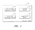
- FIG. 1 illustrates a block diagram of a satellite 100 that includes a fault tolerant processing system 110 to control various functions of the satellite 100 .
- the fault tolerant processing system 110 is connected to a thruster control module 115 that oversees the operation of the satellite thrusters.
- the fault tolerant processing system 110 is connected to a solar array deployment module 120 that includes programming to control the deployment and positioning of the solar array on the satellite.
- a communication module 125 may also be connected to the fault tolerant processing system 110 to provide communication channels between the satellite 100 and a ground station.
- the satellite 100 is provided with a system that is robust and resistant to SEUs that may otherwise affect the guidance or control of the satellite 100 .
- the satellite 100 may also include other processing modules not illustrated in FIG. 1 for maintaining a robust computing environment for the satellite 100 .
- FIG. 2 illustrates a block diagram of the fault tolerant processing system 110 shown in FIG. 1 .
- the system includes three separate computing modules 250 , 260 and 270 .
- Each computing module includes a processor.
- computing module 1 250 includes processor 210
- computing module 2 260 includes processor 211
- computing module 3 270 includes processor 212 .
- each processor includes two internal registers.
- processor 220 includes registers 214 and 215 .
- processor 211 includes registers 216 and 217
- processor 212 includes registers 218 and 219 .
- Each processor may execute instructions stored in a memory 280 . In one implementation, those instructions may be organized into an operating system module 285 and a hashing module 290 . Each processor may read instructions included in operating system module 285 or hashing module 290 . Those instructions may configure the processors to perform functions. For example, hashing module 290 may configure processors 210 , 211 , and 212 to perform a hash of at least a portion of the processor state data for its corresponding processor.
- instructions in hashing module 290 may configure processor 210 to read the state data stored in the registers 214 or 215 for the processor 210 and create a hash of that state data. Therefore, instructions within hashing module 290 executing on each of processors 215 , 217 , and 219 represent one means for hashing configured to generate hash values for a plurality of processors state data. As will be described in more detail below, by having each processor provide hashed state data for comparison, the fault tolerant processing system 110 may quickly and efficiently compare the states of each processor in the system to determine if any faults have occurred.
- fault tolerant checking unit 230 is configured to compare the hashes generated by processors 210 , 211 , and 212 when they execute instructions included in hashing module 290 .
- fault tolerant checking unit 230 may determine whether the three hashes generated by processors 210 , 211 , and 212 are equal at a periodic interval. If the hashes are not equal, the fault tolerant checking unit 230 may then determine if at least a majority of the hashes are equal. Therefore, fault tolerant checking unit 230 represents one means for comparing a plurality of hash values. This process of comparing hash values will be described in more detail below.
- creating a hash relates to a deterministic procedure that may receive variable sized input data and output other data of a fixed size.
- processor state data When processor state data is used as input to a hash function, any small change in the processor state data will result in a large and detectable change in the resultant hash value of that state data.
- the hash returned by the processors when executing instructions stored in hashing module 290 is used to determine if the state of each processor is the same and in synch with the other processors.
- SHA-1 Secure Hash Algorithm
- NIST National Security Agency
- SHA-1 is a cryptographic hash function published by the NIST as a U.S. Federal Information Processing Standard.
- SHA-1 produces a 160-bit hash value. Because the data within each hash value is substantially smaller than the data in the entire state data from each processor, the disclosed embodiment that compares hash values for each set of processor state data is more efficient than comparing the actual state data.
- the fault tolerant checking unit 230 may be further configured to re-synchronize computing modules 250 , 260 , and 270 when it determines that the three hashes generated by processors 210 , 211 , and 212 are not equal. Therefore, fault tolerant checking unit 230 represents on means for determining if a processor within each computing module is synchronized with the processors of the other computing modules. For example, fault tolerant checking unit may re-synchronize the computing modules 250 , 260 , and 270 when one, two or all three of the hashes do not match each other. In one embodiment, re-synchronizing a computing module includes restoring the processing state of the computing module that produced a minority hash.
- the processing state of a computing module that produced a minority hash may be restored based on the processing state of a computing module that produced a majority hash. For example, if computing modules 250 and 260 produced the same hash value, and computing module 270 produced a different hash value, then computing module 270 produced the minority hash and computing modules 250 and 260 produced a majority hash.
- the state value of processor 210 in majority computing module 250 may be used to restore the state value of processor 212 in minority computing module 270 .
- the state value of processor 211 in majority computing module 260 may also be used to restore the state value of processor 212 in minority computing module 270 .
- Fault tolerant checking unit 230 may also be configured to compare the outputs of computing modules 250 , 260 , and 270 .
- lines 234 , 235 , and 236 may include address lines and data lines asserted by processors 210 , 211 , and 212 .
- Fault tolerant checking unit 230 may compare the address and data lines from computing modules 250 , 260 , and 270 , and determine if corresponding lines between the three computing modules are asserting equivalent signals. This comparison may occur on every bus cycle for address lines and data lines 234 , 235 , and 236 .
- Fault tolerant checking unit 230 may determine a majority output and an optional minority output based on the signals on lines 234 , 235 , and 236 . Fault tolerant checking unit 230 may be configured to only pass majority signals on to other hardware components, for example, memory 280 . While fault tolerant checking unit 230 is shown comparing the output signals from three computing modules 250 , 260 , and 270 , which include three processors 210 , 211 , and 212 , it should be understood that fault tolerant checking unit 230 could be configured to accept a larger number of inputs. For example, a fault tolerant checking unit 230 could compare the output from 5, 7, 9, or 11 processors to determine a majority and an optional minority output signal.
- the fault tolerant checking unit 230 is connected to a main memory 280 which is used by the fault tolerant processing system 110 for storing data, instructions and programs used by the system 110 .
- memory 280 may include instructions that configure the processors 210 , 211 , and 212 , for example, by reading data from an operating system module 285 stored within the memory 280 and loading that operating system onto one or more of the processors during a restore process.
- each processor as shown in FIG. 2 may be a single processor device, or a core of one multi-processor device.
- the fault tolerant processing system may include a plurality of separate processors, such as those made by INTEL or AMD.
- each processor may be a single core of a multi-core processor make by INTEL or AMD that functions as described above.
- a mixture of single or multi-processor devices may be used as the processors in the system 110 .
- FIG. 3 illustrates another embodiment of a fault tolerant processing system 300 , but this embodiment differs from the embodiment shown in FIG. 2 by the use of separate memory banks linked to each processor.
- the system 300 includes three computing modules 360 , 370 , and 380 .
- Each computing module includes at least one processor.
- computing module 360 includes processor 330
- computing module 370 includes processor 331
- computing module 380 includes processor 332 .
- Each processor includes internal registers for storing processor state information.
- processor 330 includes internal registers 385 and 386 .
- Processor 331 includes internal registers 387 and 388
- processor 332 includes internal registers 389 and 390 .
- Each processor also includes a memory controller associated with the processor and for controlling access to a local memory storage.
- the local memory storage is cache memory.
- processor 330 includes memory controller 320 for managing access to local memory 310 .
- memory controller 321 of processor 331 manages access to local memory 311
- memory controller 322 of processor 332 manages access to local memory 312 .
- each local memory may be partitioned into a plurality of memory segments.
- local memory 312 of computing module 380 is partitioned into four memory segments in the illustrated example. These memory segments are identified as items 318 a - d.
- the local memory may be stored external to the processor, or as integrated memory stored on the processor die.
- the local memory is fast access cache memory, and the memory segments are cache memory segments.
- the local memory is standard random access memory and configured to store program data in addition to data specific for a particular processor.
- each computing module may execute instructions included in a hashing module 345 .
- Instructions in hashing module 345 may configure the processors to calculate a hash value from the state data stored in the processor registers. While hashing module 345 is illustrated as being stored in memory 390 , which is accessible to computing modules 360 , 370 , and 380 via the fault tolerant checking unit 350 , hashing module 345 may instead be stored in local memories 310 , 311 , and 312 . These local memories may provide faster access to code segments, such as those provided by hashing module 345 . In other embodiments, copies of hashing module 345 may be stored in memory 390 and local memories 310 , 311 , and 312 .
- the hashing module 345 configures the processors to create a hash that also includes data from the local memory associated with each processor. For example, when instructions included in hashing module 345 are executed by processor 330 , processor 330 may create a hash to represent the state of processor 330 and local memory 310 . Similarly, when instructions in hashing module 345 are executed by processor 331 , processor 331 may create a hash to represent the state of processor 331 and local memory 311 . When instructions in hashing module 345 are executed by processor 332 , processor 332 may create a hash to represent the state of processor 332 and local memory 312 . Therefore, instructions included in hashing module 345 running on each of processors 330 , 331 , and 332 may represent one means for hashing configured to generate hash values for the processor state data of a plurality of computing modules.
- a hash operation may include any operation that uniquely maps a large data set to a smaller data set.
- a hash may map multiple bytes that comprise processing state data stored in registers 385 and 386 into a four byte quantity.
- a hash may further map both a processing state and a memory state into a smaller data set, such as a four byte quantity.
- a hash may map the contents of processing state stored in registers 385 and 386 , along with the contents of at least a portion of local memory 310 , into a four byte quantity.
- a hash may be a checksum produced by the SHA-1 hash algorithm.
- Instructions within hashing module 345 may further configure processors 330 , 331 and 332 to vary the memory state data used to create a hash. For example, when instructions within hashing module 345 run within computing module 1 on processor 330 , a first hash may map processing state registers 385 and 386 , along with memory state data from memory segment 316 a , into a hash. In one example, the hash is a four byte hash. When a second hash is produced with processor 330 , hashing module 345 may map processing state registers 385 and 386 , along with memory segment 316 b into a hash, for example, another four byte quantity.
- hashing module 345 running on processor 330 has included all segments of memory 310 in a hash
- instructions within hashing module 345 may configure processor 330 to return to memory segment 316 a and repeat the cycle. Therefore, instructions within hashing module 345 , running on processors 330 , 331 , or 332 , represent means for hashing combined processor state data and memory state data for each computing module.
- hashing module 345 may not include instructions that configure processors 330 , 331 , and 332 to create hashes for local memories 310 , 311 , and 312 as described above.
- a separate memory coherency checking unit 352 may be provided.
- Memory coherency checking unit 352 may be configured to monitor the address, data and control lines between processors and their respective local memories. As shown, memory coherency checking unit 352 is configured to monitor the lines between processor 330 and local memory 310 via lines 354 .
- Memory coherency checking unit 352 may also monitor address, data, and control lines between processor 331 and memory 311 via lines 356 , and processor 332 and memory 312 via lines 358 .
- memory coherency checking unit 352 may be configured to detect errors in memories 310 , 311 , and 312 by identifying inconsistencies between data from the memories. Memory coherency checking unit may be further configured to signal fault tolerant checking unit 350 via separate signaling lines (not shown) upon detection of such an error condition.
- both a memory coherency checking unit 352 and a hashing module 345 may be utilized. For example, some of these embodiments may begin a re-synchronization process based on an error detected by memory coherency checking unit 352 .
- the re-synchronization process may itself be synchronized between the processing modules, as the minority and majority processing modules may have departed from lockstep operation. This synchronization may be based on an event or particular time period elapsing after initiation of a re-synchronization.
- hashing module 345 may configure the processors to hash portions of processor state data or memory state data. These hashes may be used by fault tolerant checking unit 350 to identify differences in these states between processing modules. This information may assist processing modules 360 , 370 , and 380 to return to lockstep operation.
- the system 300 may include Direct Memory Access (DMA) capabilities. These DMA capabilities may provide an ability to read and write to locations of local memories 310 , 311 , and 312 , without loading each word of memory processed into processors 330 , 331 , and 332 . This may enable data collection from the memories for hash calculation to occur substantially in parallel with the operation of processors 330 , 331 , and 332 .
- processors 330 , 331 , and 332 may include integrated DMA capabilities.
- Some embodiments may provide for additional hardware components to control the hashing process.
- dedicated hardware processors or components may control a DMA process that reads data from the memories. This data may be used to create hashes.
- Some of these embodiments may also retrieve processor state data from processors 330 , 331 , and 332 using specialized hardware components. These hardware components may then calculate hashes as appropriate based on the collected data and send the hash information to fault tolerant checking unit 350 .
- These embodiments may provide improved performance compared to embodiments that utilize existing processor capacity to periodically calculate hashes. These embodiments may also provide for increased cost.
- Each processor 330 , 331 , and 332 when running hashing module 345 may create hashes as described above for its respective computing module. The hashes from each processor may then be passed to a fault tolerant checking unit 350 .
- fault tolerant checking unit 350 is configured to compare the hashes generated by processors 330 , 331 and 332 to determine a majority hash and an optional minority hash. Fault tolerant checking unit 350 may initiate a re-synchronization of computing modules 360 , 370 , and 380 when the hashes provided by processors 330 , 331 , and 332 differ.
- a fault tolerant checking module 350 may represent one means for determining if the processor within each computing module is synchronized with the processor of the other computing modules.
- the fault tolerant checking unit 350 may initiate a re-synchronization by sending a signal to a re-synchronizing module 349 running on each processor 330 , 331 , and 332 .
- Re-synchronizing module 349 includes instructions that configure each processor to perform a re-synchronization.
- Re-synchronization module 349 may be stored as part of a memory 390 .
- the re-synchronizing of computing modules 360 , 370 , and 380 may be controlled by instructions located in the re-synchronization module 349 of FIG. 3 .
- a fault tolerant checking unit 350 along with instructions within a re-synchronization module running on each of processors 330 , 331 , and 332 represent one means for re-synchronizing a computing module based on the hashes created by processors 330 , 331 , and 332 .
- Re-synchronization module 349 may include instructions that configure each of processors 330 , 331 , and 332 to update processing state data or memory state data of a computing module that produced a minority hash.
- the processing state of a computing module that produced a minority hash may be updated based on the processing state of a computing module that produced a majority hash. For example, if computing modules 360 and 370 produced the same hash value, and computing module 380 produced a different hash value, then computing module 380 produced the minority hash and processors 360 and 370 produced a majority hash.
- the processing state data and or state data of computing module 380 may be updated based on the processing state data and memory state data of either computing module 360 or computing module 370 .
- computing module 380 may receive new state from either computing module 360 or computing module 370 .
- computing module 380 may receive new state for registers 389 and 390 from computing module 360 .
- the new state may be received from registers 385 and 386 of processor 330 .
- the new state may be transmitted directly from computing module 360 to computing module 380 via a link 361 that connects the processors 330 , 331 and 332 .
- the link 361 may be a PCI Express bus or other high speed bus with a direct connection to each processor of the system 300 .
- the new state data received from either computing module 360 or computing module 370 may also include memory state data.
- computing module 380 may receive new memory state data for portions or all of memory 312 from computing module 360 .
- the new memory state data may be received from memory 310 .
- one or more of memory segments 316 a - d may be transferred over link 361 to computing module 380 .
- Computing module 380 may then replace the contents of memory 312 with the memory state data received from computing module 360 .
- computing module 380 may replace the memory state data for one or more memory segments 318 a - d when receiving corresponding one or more memory segments 316 a - d from computing module 360 .
- some embodiments may perform an additional verification after a resynchronization process is complete. For example, these embodiments may perform an additional partial re-synchronization to determine whether the hashes generated by the processing modules match. If the computing modules that formed a majority during the preceding re-synchronization do not generate matching hashes, recovery steps may be appropriate. Alternatively, if the hash of the minority computing module does not match the hash of a majority computing module from which the minority computing module did not receive state during the previous resynchronization, recovery steps may also be appropriate. For example, an error may be flagged as a result of the comparison of these hashes. A reboot of the fault tolerant processing system board may be performed as a result of the error. While this may disrupt operations, it may return the system to verifiably correct operation.
- a link 362 may be utilized that directly connects these processors together.
- a link 364 may be utilized that directly connects these two processors together.
- Each processor may also have access to the memory bank 390 via the fault tolerant checking unit 350 .
- each processor may access memory 390 after a coherency check of the outputs of the processors, as described earlier with respect to FIG. 2 , is performed by the fault tolerant checking unit 350 .
- Local memories 310 , 311 , and 312 , or memories accessible via fault tolerant checking unit 350 , such as memory 390 may store instructions that configure processors 330 , 331 , and 332 to perform functions.
- processors 330 , 331 , and 332 may read memory locations in memory 390 via fault tolerant checking unit 350 .
- Memory 390 may include instructions that configure processors 330 , 331 and 332 .
- Memory 390 may also include instructions for an operating system (not shown), or the re-synchronization module 349 .
- each processor 330 , 331 , and 332 may read instructions from the local memory within its respective computing module.
- processor 330 may read instructions from local memory 310 .
- Processor 331 may read instructions from memory 311 and processor 332 may read instructions from local memory 312 .
- FIG. 4 is a flow chart illustrating an exemplary process 400 that may run in a fault tolerant checking unit to compare hashes received from a plurality of computing modules.
- process 400 may be implemented by instructions within fault tolerant checking unit 350 of FIG. 3 , or fault tolerant checking unit 230 of FIG. 2 .
- the process 400 begins at start block 405 and then moves to processing block 410 , where process 400 waits to initiate a partial re-synchronization.
- a partial re-synchronization of the processors may be performed periodically to ensure that each processor is in synchronization with the other processors in the system. Some embodiments may perform a partial resynchronization every 1, 2, 5, 10, 20 or more milliseconds.
- process 400 moves to processing block 415 , where the processors are signaled to perform a partial re-synchronization.
- the processors may hash their processing state data or their memory state data. Partial re-synchronization is described in FIG. 5 below.
- Process 400 then moves to processing block 420 , where hashes are received from all processing modules.
- Process 400 then moves to decision block 425 , where the hashes are evaluated to determine whether they all equivalent.
- the hashes may include separate hashes of both processor state data and memory state data of each computing module. Some implementations may combine hashes of processing state data and memory state data into a single hash value.
- the portion of the hash that represents memory state data may represent only a portion of a computing modules memory state data. Other implementations may include a representation of all of the computing modules memory state data in the hash.
- Process 400 moves to end block 450 and the process 400 terminates. If all of the hashes do not match, there may be a minority hash and at least two majority hashes. Process 400 then moves from decision block 425 to processing block 430 where the processing modules are signaled to perform a full re-synchronization.
- a full re-synchronization will synchronize the processor state data or memory state data for a computing module that generated a minority hash with the state data of a computing module that generated a majority hash.
- the re-synchronization process is described in FIG. 6 below.
- Process 400 then moves to block 435 , where process 400 sends a signal to the minority computing modules indicating that they will be receiving new state.
- Process 400 then moves to processing block 440 , where process 400 sends a signal to at least one majority computing module instructing the majority computing module that it should send new state to the minority computing module.
- Process 400 then moves to block 445 , where it waits for all computing modules to complete the re-synchronization.
- Process 400 then moves to end state 450 .
- FIG. 5 shows a flowchart of an exemplary hashing process.
- process 500 may be implemented by instructions included in hashing module 290 of FIG. 2 .
- process 500 may be implemented by instructions included in hashing module 345 of FIG. 3 .
- Process 550 begins at start state 555 and then moves to block 560 , where it waits for a partial re-synchronization signal.
- the partial re-synchronization signal may be sent by process 400 , as discussed previously.
- process 550 moves to processing block 565 , where the processor state data is hashed.
- processor 330 of computing module 360 may be configured by instructions included in hashing module 345 to hash its processor states 385 and 386 .
- Process 550 then moves to processing block 570 , where memory state data is hashed.
- processor 330 of computing module 360 may be configured by instructions included in hashing module 345 , illustrated in FIG. 3 , to hash one or more of memory portions 316 a - d .
- Process 550 then moves to block 575 , where the hash or hashes resulting from the combined hashing of the processor state data in block 565 and the memory state data in block 570 is sent to the fault tolerant checking unit.
- processor 330 may send a hash to fault tolerant checking unit 350 to implement processing block 570 .
- Process 550 then moves to end block 580 .
- FIG. 6 shows a flowchart of an exemplary process 600 that performs a full re-synchronization of a computing module.
- Process 600 may be implemented by instructions included in re-synchronization module 349 , illustrated in FIG. 3 .
- process 600 may be implemented by a re-synchronization module stored in a local memory, such as memory 310 , illustrated in FIG. 3 .
- These instructions may run on a processor within a computing module.
- the instructions may run on processor 330 of computing module 360 .
- Process 600 begins at start block 605 and then moves to processing block 610 , where process 600 waits for a full re-synchronization request.
- process 600 moves to block 615 where the processor state data is saved. For example, if processor 330 of computing module 360 receives a re-synchronization request, it may save registers 385 and 386 when implementing processing block 615 of process 600 .
- Process 600 then moves to decision block 620 , where it determines if it will receive new state. If it will receive new state, process 600 moves to block 650 , where new processor state data is received. This new state data overwrites any data saved in processing block 615 .
- Process 600 then moves to block 655 , where new memory state data is received.
- this memory state may include the state of an entire local memory, for example, local memory 310 , 311 , or 312 , illustrated in FIG. 3 .
- this memory state may include only a portion of a local memory. For example, it may include only one memory segment, for example, memory segment 316 a , 317 a , or 318 a , also illustrated in FIG. 3 .
- process 600 moves to processing block 640 , where a signal is sent that the re-synchronization is complete.
- process 600 moves to decision block 625 , where it determines if state should be sent. If no state should be sent, process 600 moves to block 640 where it signals that its re-synchronization process is complete. If at decision block 625 it is determined that the processing module running process 600 should send state, process 600 moves to processing block 630 , where the saved processor state data is sent. Process 600 then moves to processing block 635 , where new memory state data is sent.
- the memory state data sent in block 635 may include a portion or all of a local memory. For example, it may include a portion of memory 310 , for example, memory segment 316 a .
- Process 600 may include two memory segments, for example, memory segments 316 a - b . Still other implementations may send the entire memory 310 , to include memory segments 316 a - d .
- Process 600 then moves to processing block 640 , where it signals that its portion of the re-synchronization is complete. After processing block 640 , process 600 moves to block 645 , where process 600 waits for all processing modules to complete their re-synchronization events. When all processing modules have signaled (via processing block 640 ) that their re-synchronization events are complete, process 600 moves to block 670 where the saved processing state data from processing block 615 is restored and process 600 returns from the event. Process 600 then moves to end block 680 .
- FIG. 7 shows a flowchart illustrating an exemplary implementation of a hashing method.
- Process 700 may be implemented by instructions included in hashing module 345 illustrated in FIG. 3 .
- Process 700 begins at start block 710 and then moves to processing block 720 , where a hash is initialized.
- Process 700 then moves to processing block 730 , where the processing state data is hashed.
- processor 330 may be configured by instructions in hashing module 345 to hash its processor states 385 and 386 to implement processing block 723 .
- Process 700 then moves to decision block 740 , where it determines whether a full memory hash will be performed or a partial memory hash will be performed.
- Process 700 moves to processing block 750 if a full memory hash will be performed.
- Processing block 750 may include the entire memory contents when determining the hash value. If decision block 740 determines that only a portion of the memory will be included in the hash, process 700 moves to processing block 780 , where a local memory segment identifier is incremented. Process 700 then moves to block 790 , where the hashing is continued with the memory segment identified by the segment identifier.
- a local memory segment identifier may track a memory segment that should be included in the hash. For example, some implementations may vary the memory segment included in the hash for each partial re-synchronization. Some implementations may include the first memory segment in the first hash that is created. Each subsequent partial re-synchronization may include a different memory segment as part of the hash value. For example, the second partial re-synchronization may include a second memory segment, and a third partial re-synchronization may include a third memory segment. When all memory segments of a memory have been included as part of a partial resynchronization, the process 700 may again use the contents of the first memory segment in a hash. This incremental inclusion of different memory segments may then repeat.
- process 700 moves to block 760 , where the hash is provided.
- the hash may be provided to fault tolerant checking unit 350 , illustrated in FIG. 3 .
- Process 700 then moves to end block 770 .
- FIG. 8 shows a flowchart illustrating an exemplary receive memory process 655 .
- Process 655 may be implemented by instructions included in re-synchronization module 349 , illustrated in FIG. 3 .
- process 655 may be implemented by instructions stored in local memories 310 , 311 or 312 , also illustrated in FIG. 3 .
- Process 655 begins at start block 805 and then moves to decision block 810 where it determines whether the computing module running process 655 will be receiving a full memory image or a partial memory image. If receiving a full memory image, process 655 moves to processing block 820 , where the full memory image is received.
- computing module 360 may receive a memory image for local memory 310 .
- This image may include new memory state data for each memory segment of local memory 310 , to include memory segments 316 a - d .
- Process 655 then moves to end block 850 .
- process 655 determines that only a partial memory image may be received, process 655 moves to block 830 , where a memory segment is received.
- computing module 360 may receive an image for a memory segment of local memory 310 .
- an image for only memory segment 316 a may be received in processing block 830 .
- Process 655 then moves to block 840 , where the received local memory segment replaces a memory segment based on the segment id.
- the segment id referenced in block 840 may be the same segment id as that referenced in block 780 of process 700 , illustrated in FIG. 7 .
- Process 655 then moves to end block 850 .
- FIG. 9 shows a flowchart illustrating an exemplary memory sending process 635 .
- Process 635 may be implemented by instructions included in re-synchronization module 349 , illustrated in FIG. 3 .
- Process 635 begins at start block 905 and then moves to decision block 910 , where a determination is made whether a full memory state will be sent or a partial memory state will be sent. If a full memory state will be sent, process 635 moves to block 920 where the full memory state is sent. Process 635 then moves to end block 950 . If a partial memory image will be sent, process 635 moves to block 935 , where the memory segment is identified based on a segment identifier.
- the segment identifier referenced in block 930 may be the same identifier referenced in block 780 , illustrated in FIG. 7 .
- Process 635 then moves to block 940 , where the memory segment identified by the segment identifier is sent.
- Process 635 then moves to end block 950 .
- FIG. 10 shows a flowchart illustrating an exemplary memory sending and receiving process.
- Process 1000 may be an alternative implementation to processes 635 or 655 , discussed previously.
- Process 1000 may be implemented by instructions included in hashing module 345 or re-synchronization module 349 , of a combination of the two modules, illustrated in FIG. 3 .
- Multiple processing modules such as processing modules 360 , 370 , and 380 , illustrated in FIG. 3 , may perform process 1000 substantially simultaneously in order to coordinate a resynchronization of local memory contents between the processing modules.
- Process 1000 begins at start block 1005 and then moves to block 1010 where a portion identifier is initialized. This portion identifier may be utilized to identify a portion of a memory, such as portions of local memories 310 . 311 . or 312 . In some embodiments, a portion of a memory may be a memory segment. Process 1000 then moves to block 1015 , where a portion of memory is hashed based on the identifier. Process 1000 then moves to block 1020 , where the hash is sent to a fault tolerant checking unit, for example fault tolerant checking unit 350 of FIG. 3 .
- a fault tolerant checking unit for example fault tolerant checking unit 350 of FIG. 3 .
- Process 1000 then moves to block 1025 and waits for a response.
- Process 1000 may be waiting for a response from a fault tolerant checking unit.
- fault tolerant checking unit may compare hashes sent to it by computing modules 360 , 370 , and 380 performing process 1000 .
- decision block 1030 it is determined whether the received hashes match.
- fault tolerant checking module 350 may send a response to a processing modules running process 1000 , indicating whether the hash calculated in processing block 1015 matched hashes created by other processing modules, also running process 1000 . If the hashes did match, process 1000 moves to decision block 1050 .
- process 1000 moves to decision block 1035 , where it determines whether this particular instance of process 1000 will be sending or receiving data. If the hashes did not match, one processing module may have created a minority hash. A processing module creating a minority hash and running process 1000 may receive a new portion of memory, so as to re-synchronize with the processing modules that created majority hashes. The minority processing module may move from decision block 1035 to block 1045 . In block 1045 , process 1000 may receive a new memory portion from another processing module, for example a processing module that created a majority hash.
- Another computing module performing process 1000 may have created a majority hash. This processing module may determine in decision block 1035 that it will send a portion of memory to a processing module that created a minority hash. In this case, this processing module may move from decision block 1035 to block 1040 .
- process 1000 moves to decision block 1050 , where it determines whether there are additional memory portions that should be synchronized. If there are no remaining portions, process 1000 moves to end state 1060 . If there are remaining portions, process 1000 moves to block 1055 , where the memory portion identifier is incremented. Process 1000 then returns to block 1015 and the memory portion identified by the identifier incremented in block 1055 is hashed. Process 1000 then repeats as described above.
- the hardware and data processing apparatus used to implement the various illustrative logics, logical blocks, modules and circuits described in connection with the aspects disclosed herein may be implemented or performed with a general purpose single- or multi-chip processor, a digital signal processor (DSP), an application specific integrated circuit (ASIC), a field programmable gate array (FPGA) or other programmable logic device, discrete gate or transistor logic, discrete hardware components, or any combination thereof designed to perform the functions described herein.
- a general purpose processor may be a microprocessor, or, any conventional processor, controller, microcontroller, or state machine.
- a processor also may be implemented as a combination of computing modules, e.g., a combination of a DSP and a microprocessor, a plurality of microprocessors, one or more microprocessors in conjunction with a DSP core, or any other such configuration.
- particular steps and methods may be performed by circuitry that is specific to a given function.
- the functions described may be implemented in hardware, digital electronic circuitry, computer software, firmware, including the structures disclosed in this specification and their structural equivalents thereof, or in any combination thereof. Implementations of the subject matter described in this specification also can be implemented as one or more computer programs, i.e., one or more modules of computer program instructions, encoded on a computer storage media for execution by, or to control the operation of, data processing apparatus.
Landscapes
- Engineering & Computer Science (AREA)
- Theoretical Computer Science (AREA)
- Quality & Reliability (AREA)
- Physics & Mathematics (AREA)
- General Engineering & Computer Science (AREA)
- General Physics & Mathematics (AREA)
- Hardware Redundancy (AREA)
Priority Applications (1)
| Application Number | Priority Date | Filing Date | Title |
|---|---|---|---|
| US13/284,647 US8930753B2 (en) | 2010-10-28 | 2011-10-28 | System, method and apparatus for error correction in multi-processor systems |
Applications Claiming Priority (2)
| Application Number | Priority Date | Filing Date | Title |
|---|---|---|---|
| US40777010P | 2010-10-28 | 2010-10-28 | |
| US13/284,647 US8930753B2 (en) | 2010-10-28 | 2011-10-28 | System, method and apparatus for error correction in multi-processor systems |
Publications (2)
| Publication Number | Publication Date |
|---|---|
| US20120117419A1 US20120117419A1 (en) | 2012-05-10 |
| US8930753B2 true US8930753B2 (en) | 2015-01-06 |
Family
ID=45994441
Family Applications (1)
| Application Number | Title | Priority Date | Filing Date |
|---|---|---|---|
| US13/284,647 Expired - Fee Related US8930753B2 (en) | 2010-10-28 | 2011-10-28 | System, method and apparatus for error correction in multi-processor systems |
Country Status (5)
| Country | Link |
|---|---|
| US (1) | US8930753B2 (ru) |
| EP (1) | EP2633408B1 (ru) |
| ES (1) | ES2694803T3 (ru) |
| RU (1) | RU2577465C2 (ru) |
| WO (1) | WO2012058597A1 (ru) |
Cited By (3)
| Publication number | Priority date | Publication date | Assignee | Title |
|---|---|---|---|---|
| US20140164839A1 (en) * | 2011-08-24 | 2014-06-12 | Tadanobu Toba | Programmable device, method for reconfiguring programmable device, and electronic device |
| US9230650B2 (en) * | 2013-10-21 | 2016-01-05 | SK Hynix Inc. | Semiconductor device and method for operating the same |
| US20170168902A1 (en) * | 2015-12-15 | 2017-06-15 | Intel Corporation | Processor state integrity protection using hash verification |
Families Citing this family (10)
| Publication number | Priority date | Publication date | Assignee | Title |
|---|---|---|---|---|
| US9003228B2 (en) * | 2012-12-07 | 2015-04-07 | International Business Machines Corporation | Consistency of data in persistent memory |
| US10210351B2 (en) | 2014-07-21 | 2019-02-19 | Servicenow, Inc. | Fingerprint-based configuration typing and classification |
| US9612985B1 (en) * | 2014-08-19 | 2017-04-04 | Rockwell Collins, Inc. | Synchronization mechanisms for high-integrity computing |
| US10481963B1 (en) * | 2016-06-29 | 2019-11-19 | Amazon Technologies, Inc. | Load-balancing for achieving transaction fault tolerance |
| EP3315977A1 (en) * | 2016-10-31 | 2018-05-02 | Rohde & Schwarz GmbH & Co. KG | Measuring device for measuring signals and data handling method |
| US11108542B2 (en) * | 2017-07-07 | 2021-08-31 | Board Of Regents Of The Nevada System Of Higher Education, On Behalf Of The University Of Nevada, Reno | Multi-processor automotive electronic control unit |
| CN108306740B (zh) * | 2018-01-22 | 2020-07-31 | 华中科技大学 | 一种Intel SGX状态一致保护方法和系统 |
| US10922203B1 (en) * | 2018-09-21 | 2021-02-16 | Nvidia Corporation | Fault injection architecture for resilient GPU computing |
| US10831383B2 (en) | 2018-11-02 | 2020-11-10 | Hamilton Sundstrand Corporation | Command line voting using hashing |
| CN113076065B (zh) * | 2021-04-14 | 2022-12-09 | 中国人民解放军国防科技大学 | 一种高性能计算系统中数据输出故障容错方法 |
Citations (25)
| Publication number | Priority date | Publication date | Assignee | Title |
|---|---|---|---|---|
| US4414624A (en) | 1980-11-19 | 1983-11-08 | The United States Of America As Represented By The Secretary Of The Navy | Multiple-microcomputer processing |
| US5189647A (en) | 1991-02-25 | 1993-02-23 | International Business Machines Corp. | Information processing system having power saving control of the processor clock |
| US5630148A (en) | 1994-06-17 | 1997-05-13 | Intel Corporation | Dynamic processor performance and power management in a computer system |
| US5956474A (en) | 1993-12-01 | 1999-09-21 | Marathon Technologies Corporation | Fault resilient/fault tolerant computing |
| US6247143B1 (en) * | 1998-06-30 | 2001-06-12 | Sun Microsystems, Inc. | I/O handling for a multiprocessor computer system |
| US20040030966A1 (en) | 2002-08-12 | 2004-02-12 | Spieker Thomas L. | System, method, and apparatus for detecting and recovering from false synchronization |
| US20040073822A1 (en) | 2002-04-03 | 2004-04-15 | Hewlett-Packard Development Company, L.P. | Data processing system and method |
| US6751749B2 (en) * | 2001-02-22 | 2004-06-15 | International Business Machines Corporation | Method and apparatus for computer system reliability |
| US20040193735A1 (en) | 2002-09-12 | 2004-09-30 | Pavel Peleska | Method and circuit arrangement for synchronization of synchronously or asynchronously clocked processor units |
| US6834354B1 (en) | 1999-06-16 | 2004-12-21 | Sony Corporation | Method and apparatus for assigning tasks in an information processing system to optimize power consumption versus performance of the system |
| US20050160312A1 (en) * | 2002-03-20 | 2005-07-21 | Wouter Seng | Fault-tolerant computers |
| US6938183B2 (en) * | 2001-09-21 | 2005-08-30 | The Boeing Company | Fault tolerant processing architecture |
| US6986068B2 (en) | 2000-09-22 | 2006-01-10 | Sony Corporation | Arithmetic processing system and arithmetic processing control method, task management system and task management method |
| US20060020852A1 (en) | 2004-03-30 | 2006-01-26 | Bernick David L | Method and system of servicing asynchronous interrupts in multiple processors executing a user program |
| US20060020850A1 (en) * | 2004-07-20 | 2006-01-26 | Jardine Robert L | Latent error detection |
| US20060236168A1 (en) * | 2005-04-01 | 2006-10-19 | Honeywell International Inc. | System and method for dynamically optimizing performance and reliability of redundant processing systems |
| US20070052453A1 (en) | 2005-09-08 | 2007-03-08 | Wald Steven F | Method and apparatus for monitoring and controlling the thermal environment and operating conditions of an integrated circuit |
| US7310759B1 (en) * | 2001-02-14 | 2007-12-18 | Xilinx, Inc. | Techniques for mitigating, detecting, and correcting single event upset effects in systems using SRAM-based field programmable gate arrays |
| US7589558B1 (en) * | 2008-02-27 | 2009-09-15 | Xilinx, Inc. | Method and apparatus for configuring an integrated circuit |
| US20090327818A1 (en) | 2007-04-27 | 2009-12-31 | Network Appliance, Inc. | Multi-core engine for detecting bit errors |
| US7797575B2 (en) * | 2007-04-04 | 2010-09-14 | International Business Machines Corporation | Triple voting cell processors for single event upset protection |
| US7996714B2 (en) * | 2008-04-14 | 2011-08-09 | Charles Stark Draper Laboratory, Inc. | Systems and methods for redundancy management in fault tolerant computing |
| US20110208997A1 (en) * | 2009-12-07 | 2011-08-25 | SPACE MICRO, INC., a corporation of Delaware | Radiation hard and fault tolerant multicore processor and method for ionizing radiation environment |
| US8117512B2 (en) * | 2008-02-06 | 2012-02-14 | Westinghouse Electric Company Llc | Failure detection and mitigation in logic circuits |
| US8140893B2 (en) * | 2009-03-18 | 2012-03-20 | Nec Corporation | Fault-tolerant system |
Family Cites Families (1)
| Publication number | Priority date | Publication date | Assignee | Title |
|---|---|---|---|---|
| US5799022A (en) * | 1996-07-01 | 1998-08-25 | Sun Microsystems, Inc. | Faulty module location in a fault tolerant computer system |
-
2011
- 2011-10-28 EP EP11837198.8A patent/EP2633408B1/en not_active Not-in-force
- 2011-10-28 ES ES11837198.8T patent/ES2694803T3/es active Active
- 2011-10-28 WO PCT/US2011/058394 patent/WO2012058597A1/en active Application Filing
- 2011-10-28 RU RU2013123176/08A patent/RU2577465C2/ru not_active IP Right Cessation
- 2011-10-28 US US13/284,647 patent/US8930753B2/en not_active Expired - Fee Related
Patent Citations (26)
| Publication number | Priority date | Publication date | Assignee | Title |
|---|---|---|---|---|
| US4414624A (en) | 1980-11-19 | 1983-11-08 | The United States Of America As Represented By The Secretary Of The Navy | Multiple-microcomputer processing |
| US5189647A (en) | 1991-02-25 | 1993-02-23 | International Business Machines Corp. | Information processing system having power saving control of the processor clock |
| US5956474A (en) | 1993-12-01 | 1999-09-21 | Marathon Technologies Corporation | Fault resilient/fault tolerant computing |
| US5630148A (en) | 1994-06-17 | 1997-05-13 | Intel Corporation | Dynamic processor performance and power management in a computer system |
| US6247143B1 (en) * | 1998-06-30 | 2001-06-12 | Sun Microsystems, Inc. | I/O handling for a multiprocessor computer system |
| US6834354B1 (en) | 1999-06-16 | 2004-12-21 | Sony Corporation | Method and apparatus for assigning tasks in an information processing system to optimize power consumption versus performance of the system |
| US6986068B2 (en) | 2000-09-22 | 2006-01-10 | Sony Corporation | Arithmetic processing system and arithmetic processing control method, task management system and task management method |
| US7310759B1 (en) * | 2001-02-14 | 2007-12-18 | Xilinx, Inc. | Techniques for mitigating, detecting, and correcting single event upset effects in systems using SRAM-based field programmable gate arrays |
| US6751749B2 (en) * | 2001-02-22 | 2004-06-15 | International Business Machines Corporation | Method and apparatus for computer system reliability |
| US6938183B2 (en) * | 2001-09-21 | 2005-08-30 | The Boeing Company | Fault tolerant processing architecture |
| US20050160312A1 (en) * | 2002-03-20 | 2005-07-21 | Wouter Seng | Fault-tolerant computers |
| US20040073822A1 (en) | 2002-04-03 | 2004-04-15 | Hewlett-Packard Development Company, L.P. | Data processing system and method |
| US20040030966A1 (en) | 2002-08-12 | 2004-02-12 | Spieker Thomas L. | System, method, and apparatus for detecting and recovering from false synchronization |
| US20040193735A1 (en) | 2002-09-12 | 2004-09-30 | Pavel Peleska | Method and circuit arrangement for synchronization of synchronously or asynchronously clocked processor units |
| US20060020852A1 (en) | 2004-03-30 | 2006-01-26 | Bernick David L | Method and system of servicing asynchronous interrupts in multiple processors executing a user program |
| US20060020850A1 (en) * | 2004-07-20 | 2006-01-26 | Jardine Robert L | Latent error detection |
| US20060236168A1 (en) * | 2005-04-01 | 2006-10-19 | Honeywell International Inc. | System and method for dynamically optimizing performance and reliability of redundant processing systems |
| US7515996B2 (en) | 2005-09-08 | 2009-04-07 | Avago Technologies General Ip (Singapore) Pte. Ltd. | Method and apparatus for monitoring and controlling the thermal environment and operating conditions of an integrated circuit |
| US20070052453A1 (en) | 2005-09-08 | 2007-03-08 | Wald Steven F | Method and apparatus for monitoring and controlling the thermal environment and operating conditions of an integrated circuit |
| US7797575B2 (en) * | 2007-04-04 | 2010-09-14 | International Business Machines Corporation | Triple voting cell processors for single event upset protection |
| US20090327818A1 (en) | 2007-04-27 | 2009-12-31 | Network Appliance, Inc. | Multi-core engine for detecting bit errors |
| US8117512B2 (en) * | 2008-02-06 | 2012-02-14 | Westinghouse Electric Company Llc | Failure detection and mitigation in logic circuits |
| US7589558B1 (en) * | 2008-02-27 | 2009-09-15 | Xilinx, Inc. | Method and apparatus for configuring an integrated circuit |
| US7996714B2 (en) * | 2008-04-14 | 2011-08-09 | Charles Stark Draper Laboratory, Inc. | Systems and methods for redundancy management in fault tolerant computing |
| US8140893B2 (en) * | 2009-03-18 | 2012-03-20 | Nec Corporation | Fault-tolerant system |
| US20110208997A1 (en) * | 2009-12-07 | 2011-08-25 | SPACE MICRO, INC., a corporation of Delaware | Radiation hard and fault tolerant multicore processor and method for ionizing radiation environment |
Non-Patent Citations (2)
| Title |
|---|
| International Search Report and Written Opinion issued in International Application No. PCT/US2011/58394 on Mar. 16, 2012. |
| Notification of Transmittal of the International Search Report and Written Opinion issued in Corresponding International Patent Application No. PCT/US2011/58394 on Mar. 16, 2012. |
Cited By (4)
| Publication number | Priority date | Publication date | Assignee | Title |
|---|---|---|---|---|
| US20140164839A1 (en) * | 2011-08-24 | 2014-06-12 | Tadanobu Toba | Programmable device, method for reconfiguring programmable device, and electronic device |
| US9230650B2 (en) * | 2013-10-21 | 2016-01-05 | SK Hynix Inc. | Semiconductor device and method for operating the same |
| US20170168902A1 (en) * | 2015-12-15 | 2017-06-15 | Intel Corporation | Processor state integrity protection using hash verification |
| US10185633B2 (en) * | 2015-12-15 | 2019-01-22 | Intel Corporation | Processor state integrity protection using hash verification |
Also Published As
| Publication number | Publication date |
|---|---|
| EP2633408A1 (en) | 2013-09-04 |
| US20120117419A1 (en) | 2012-05-10 |
| RU2013123176A (ru) | 2014-12-10 |
| ES2694803T3 (es) | 2018-12-27 |
| EP2633408A4 (en) | 2017-06-14 |
| EP2633408B1 (en) | 2018-08-22 |
| WO2012058597A1 (en) | 2012-05-03 |
| RU2577465C2 (ru) | 2016-03-20 |
Similar Documents
| Publication | Publication Date | Title |
|---|---|---|
| US8930753B2 (en) | System, method and apparatus for error correction in multi-processor systems | |
| US7613948B2 (en) | Cache coherency during resynchronization of self-correcting computer | |
| US5903717A (en) | Fault tolerant computer system | |
| US9052887B2 (en) | Fault tolerance of data processing steps operating in either a parallel operation mode or a non-synchronous redundant operation mode | |
| US7272681B2 (en) | System having parallel data processors which generate redundant effector date to detect errors | |
| US6938183B2 (en) | Fault tolerant processing architecture | |
| US8635492B2 (en) | State recovery and lockstep execution restart in a system with multiprocessor pairing | |
| US20090044044A1 (en) | Device and method for correcting errors in a system having at least two execution units having registers | |
| US20060190702A1 (en) | Device and method for correcting errors in a processor having two execution units | |
| US7797575B2 (en) | Triple voting cell processors for single event upset protection | |
| US20100318746A1 (en) | Memory change track logging | |
| US20090037765A1 (en) | Systems and methods for maintaining lock step operation | |
| JPH07129426A (ja) | 障害処理方式 | |
| US9170907B2 (en) | Method of providing high integrity processing | |
| US20040153731A1 (en) | Information processing apparatus | |
| US20200272533A1 (en) | Detecting memory mismatch between lockstep systems using a memory signature | |
| Szurman et al. | Towards a state synchronization methodology for recovery process after partial reconfiguration of fault tolerant systems | |
| CN115698953A (zh) | 用于锁步处理器中的自动恢复的系统和方法 | |
| Liu et al. | A survey of fault tolerance hardware architecture | |
| Szurman et al. | Coarse-Grained TMR Soft-Core Processor Fault Tolerance Methods and State Synchronization for Run-Time Fault Recovery | |
| US9542266B2 (en) | Semiconductor integrated circuit and method of processing in semiconductor integrated circuit | |
| El Salloum et al. | Recovery mechanisms for dual core architectures |
Legal Events
| Date | Code | Title | Description |
|---|---|---|---|
| STCF | Information on status: patent grant |
Free format text: PATENTED CASE |
|
| AS | Assignment |
Owner name: EAST WEST BANK, CALIFORNIA Free format text: SECURITY INTEREST;ASSIGNOR:MAXWELL TECHNOLOGIES, INC.;REEL/FRAME:036064/0636 Effective date: 20150703 |
|
| AS | Assignment |
Owner name: MAXWELL TECHNOLOGIES, INC., CALIFORNIA Free format text: ASSIGNMENT OF ASSIGNORS INTEREST;ASSIGNORS:HILLMAN, ROBERT;WILLIAMSON, GALE;SIGNING DATES FROM 20111216 TO 20111219;REEL/FRAME:037688/0276 |
|
| AS | Assignment |
Owner name: MAXWELL TECHNOLOGIES, INC., CALIFORNIA Free format text: ASSIGNEE CHANGE OF ADDRESS;ASSIGNOR:MAXWELL TECHNOLOGIES, INC.;REEL/FRAME:037856/0869 Effective date: 20160212 |
|
| AS | Assignment |
Owner name: MAXWELL TECHNOLOGIES, INC., CALIFORNIA Free format text: RELEASE BY SECURED PARTY;ASSIGNOR:EAST WEST BANK;REEL/FRAME:038288/0495 Effective date: 20160412 |
|
| AS | Assignment |
Owner name: DATA DEVICE CORPORATION, NEW YORK Free format text: PATENT ASSIGNMENT;ASSIGNOR:MAXWELL TECHNOLOGIES, INC.;REEL/FRAME:038608/0509 Effective date: 20160427 |
|
| AS | Assignment |
Owner name: GCI CAPITAL MARKETS LLC, AS COLLATERAL AGENT, ILLI Free format text: SECURITY INTEREST;ASSIGNOR:DATA DEVICE CORPORATION;REEL/FRAME:038652/0062 Effective date: 20160510 |
|
| AS | Assignment |
Owner name: DATA DEVICE CORPORATION, NEW YORK Free format text: RELEASE BY SECURED PARTY;ASSIGNOR:GOLUB CAPITAL MARKETS LLC, FORMERLY KNOWN AS GCI CAPITAL MARKETS LLC, AS COLLATERAL AGENT;REEL/FRAME:038997/0516 Effective date: 20160623 |
|
| AS | Assignment |
Owner name: CREDIT SUISSE AG, AS ADMINISTRATIVE AGENT, NEW YOR Free format text: SECURITY AGREEMENT;ASSIGNOR:DATA DEVICE CORPORATION;REEL/FRAME:039537/0075 Effective date: 20160729 |
|
| FEPP | Fee payment procedure |
Free format text: ENTITY STATUS SET TO UNDISCOUNTED (ORIGINAL EVENT CODE: BIG.) |
|
| MAFP | Maintenance fee payment |
Free format text: PAYMENT OF MAINTENANCE FEE, 4TH YEAR, LARGE ENTITY (ORIGINAL EVENT CODE: M1551) Year of fee payment: 4 |
|
| AS | Assignment |
Owner name: MAXWELL TECHNOLOGIES, INC., CALIFORNIA Free format text: RELEASE BY SECURED PARTY;ASSIGNOR:EAST WEST BANK;REEL/FRAME:051441/0005 Effective date: 20190524 |
|
| FEPP | Fee payment procedure |
Free format text: MAINTENANCE FEE REMINDER MAILED (ORIGINAL EVENT CODE: REM.); ENTITY STATUS OF PATENT OWNER: LARGE ENTITY |
|
| LAPS | Lapse for failure to pay maintenance fees |
Free format text: PATENT EXPIRED FOR FAILURE TO PAY MAINTENANCE FEES (ORIGINAL EVENT CODE: EXP.); ENTITY STATUS OF PATENT OWNER: LARGE ENTITY |
|
| STCH | Information on status: patent discontinuation |
Free format text: PATENT EXPIRED DUE TO NONPAYMENT OF MAINTENANCE FEES UNDER 37 CFR 1.362 |
|
| FP | Lapsed due to failure to pay maintenance fee |
Effective date: 20230106 |