US8922029B2 - Apparatus having a wiring board and memory devices - Google Patents
Apparatus having a wiring board and memory devices Download PDFInfo
- Publication number
- US8922029B2 US8922029B2 US13/363,396 US201213363396A US8922029B2 US 8922029 B2 US8922029 B2 US 8922029B2 US 201213363396 A US201213363396 A US 201213363396A US 8922029 B2 US8922029 B2 US 8922029B2
- Authority
- US
- United States
- Prior art keywords
- wiring board
- node
- nodes
- line portion
- line
- Prior art date
- Legal status (The legal status is an assumption and is not a legal conclusion. Google has not performed a legal analysis and makes no representation as to the accuracy of the status listed.)
- Active
Links
- 230000015654 memory Effects 0.000 abstract description 59
- 230000000630 rising effect Effects 0.000 description 17
- 238000010586 diagram Methods 0.000 description 16
- 230000005540 biological transmission Effects 0.000 description 3
- 230000003111 delayed effect Effects 0.000 description 3
- 238000011156 evaluation Methods 0.000 description 3
- 239000004065 semiconductor Substances 0.000 description 3
- 229910000679 solder Inorganic materials 0.000 description 3
- 230000010365 information processing Effects 0.000 description 2
- 238000004088 simulation Methods 0.000 description 2
- 230000009977 dual effect Effects 0.000 description 1
- 230000000694 effects Effects 0.000 description 1
- 230000001939 inductive effect Effects 0.000 description 1
- 238000000034 method Methods 0.000 description 1
- 230000008054 signal transmission Effects 0.000 description 1
- UJFARQSHFFWJHD-UHFFFAOYSA-M sodium [4-[[2-[4-bromo-3-(3-chloro-5-cyanophenoxy)-2-fluorophenyl]acetyl]amino]-3-chlorophenyl]sulfonyl-propanoylazanide Chemical compound [Na+].ClC1=CC(S(=O)(=O)[N-]C(=O)CC)=CC=C1NC(=O)CC1=CC=C(Br)C(OC=2C=C(C=C(Cl)C=2)C#N)=C1F UJFARQSHFFWJHD-UHFFFAOYSA-M 0.000 description 1
- 230000001360 synchronised effect Effects 0.000 description 1
Images


Classifications
-
- G—PHYSICS
- G11—INFORMATION STORAGE
- G11C—STATIC STORES
- G11C5/00—Details of stores covered by group G11C11/00
- G11C5/06—Arrangements for interconnecting storage elements electrically, e.g. by wiring
- G11C5/063—Voltage and signal distribution in integrated semi-conductor memory access lines, e.g. word-line, bit-line, cross-over resistance, propagation delay
-
- G—PHYSICS
- G11—INFORMATION STORAGE
- G11C—STATIC STORES
- G11C5/00—Details of stores covered by group G11C11/00
- G11C5/02—Disposition of storage elements, e.g. in the form of a matrix array
- G11C5/04—Supports for storage elements, e.g. memory modules; Mounting or fixing of storage elements on such supports
-
- G—PHYSICS
- G11—INFORMATION STORAGE
- G11C—STATIC STORES
- G11C8/00—Arrangements for selecting an address in a digital store
- G11C8/14—Word line organisation; Word line lay-out
-
- H—ELECTRICITY
- H05—ELECTRIC TECHNIQUES NOT OTHERWISE PROVIDED FOR
- H05K—PRINTED CIRCUITS; CASINGS OR CONSTRUCTIONAL DETAILS OF ELECTRIC APPARATUS; MANUFACTURE OF ASSEMBLAGES OF ELECTRICAL COMPONENTS
- H05K1/00—Printed circuits
- H05K1/18—Printed circuits structurally associated with non-printed electric components
- H05K1/181—Printed circuits structurally associated with non-printed electric components associated with surface mounted components
-
- H—ELECTRICITY
- H05—ELECTRIC TECHNIQUES NOT OTHERWISE PROVIDED FOR
- H05K—PRINTED CIRCUITS; CASINGS OR CONSTRUCTIONAL DETAILS OF ELECTRIC APPARATUS; MANUFACTURE OF ASSEMBLAGES OF ELECTRICAL COMPONENTS
- H05K2201/00—Indexing scheme relating to printed circuits covered by H05K1/00
- H05K2201/09—Shape and layout
- H05K2201/09209—Shape and layout details of conductors
- H05K2201/09218—Conductive traces
- H05K2201/09254—Branched layout
-
- H—ELECTRICITY
- H05—ELECTRIC TECHNIQUES NOT OTHERWISE PROVIDED FOR
- H05K—PRINTED CIRCUITS; CASINGS OR CONSTRUCTIONAL DETAILS OF ELECTRIC APPARATUS; MANUFACTURE OF ASSEMBLAGES OF ELECTRICAL COMPONENTS
- H05K2201/00—Indexing scheme relating to printed circuits covered by H05K1/00
- H05K2201/09—Shape and layout
- H05K2201/09209—Shape and layout details of conductors
- H05K2201/09218—Conductive traces
- H05K2201/09263—Meander
-
- H—ELECTRICITY
- H05—ELECTRIC TECHNIQUES NOT OTHERWISE PROVIDED FOR
- H05K—PRINTED CIRCUITS; CASINGS OR CONSTRUCTIONAL DETAILS OF ELECTRIC APPARATUS; MANUFACTURE OF ASSEMBLAGES OF ELECTRICAL COMPONENTS
- H05K2201/00—Indexing scheme relating to printed circuits covered by H05K1/00
- H05K2201/10—Details of components or other objects attached to or integrated in a printed circuit board
- H05K2201/10007—Types of components
- H05K2201/10159—Memory
-
- Y—GENERAL TAGGING OF NEW TECHNOLOGICAL DEVELOPMENTS; GENERAL TAGGING OF CROSS-SECTIONAL TECHNOLOGIES SPANNING OVER SEVERAL SECTIONS OF THE IPC; TECHNICAL SUBJECTS COVERED BY FORMER USPC CROSS-REFERENCE ART COLLECTIONS [XRACs] AND DIGESTS
- Y02—TECHNOLOGIES OR APPLICATIONS FOR MITIGATION OR ADAPTATION AGAINST CLIMATE CHANGE
- Y02P—CLIMATE CHANGE MITIGATION TECHNOLOGIES IN THE PRODUCTION OR PROCESSING OF GOODS
- Y02P70/00—Climate change mitigation technologies in the production process for final industrial or consumer products
- Y02P70/50—Manufacturing or production processes characterised by the final manufactured product
Definitions
- the present invention relates to a printed wiring board having semiconductor elements mounted thereon, and in particular to an address line wiring structure in a memory board having a memory mounted thereon.
- a stub structure is employed for memory signal wiring in which branch lines are branched at branch points on a main line.
- an SSTL (Stub Series Terminated Logic) method is employed for data signals to minimize reflected waves at branch points, in which a resistance element having an impedance value corresponding to a half of a characteristic impedance of a signal line is inserted on the branch line side of each branch point (see, for example, Patent Documents 1 and 2 and Non-Patent Document 1).
- Patent Document 1 Japanese Laid-Open Patent Publication Nos. H07-250104
- Patent Document 2 Japanese Laid-Open Patent Publication Nos. 2004-62530
- Non-Patent Document 1 Elpida Memory User Manual, “How to Use DDR-SDRAM (Double Data Rate Synchronous Dynamic Random Access Memory)”, Chapter 1, p. 14, 1.1.4 Interface, (4) Interface Specifications
- Patent Document 2 discloses a memory module comprising a memory chip, a pin for connecting the memory chip to a connector on a mother board, a bus for connecting between the memory chip and the pin, and a terminating resistor connected to an end of the bus.
- a stub resistor is inserted and connected between the pin and the other end of the bus.
- address signals are transferred through a branch line having no inserted resistor since the address signals have a transmission speed of a half the transmission speed of data signals.
- the signal transmission speed is increased, the signal speed along the address line is also increased.
- the present inventors have recognized that waveform distortion, rising waveform blunting, or a jitter will possibly make it impossible to transmit address signals properly.
- the present invention seeks to solve the above problem.
- an address line wiring structure comprising an address signal line that connects between at least three memory elements and a data transferring element for transferring data among the at least three memory elements and that transmits address signals for the memory elements.
- the address signal line has a stub structure including branch lines branched from a main line to the respective memory elements.
- an address terminal of the data transferring element has an output impedance lower than a characteristic impedance of the address signal line.
- a wiring length TL 0 from the data transferring element to a first branch point S 1 where a branch line is branched at a shortest distance from the data transferring element is configured to become substantially equal to or greater than a wiring length TL 1 from the first branch point S 1 to a second branch point S 2 where a second branch line is branched.
- a wiring length TL 3 from the second branch point S 2 to a third branch point S 3 where a third branch line is branched is configured to become greater than the wiring lengths TL 0 and TL 1 .
- negative reflected waves generated at the second branch point S 2 and positive reflected waves that are obtained by the data transferring element reflecting negative reflected waves generated at the first branch point S 1 are canceled with each other.
- the negative reflected waves reflected at the third branch point S 3 reach the memory element on the second branch line at a time after a threshold voltage used for distinguishing the “0” level and the “1” level has been exceeded, whereby waveform distortion and delay can be prevented in the vicinity thereof.
- a wiring structure comprising a buffer circuit that generates a signal and a bus line including a first part connected between the buffer circuit and a first node, a second part connected between the first node and a second node, and a third part connected between the second node and a third node.
- the second part is substantially equal to or smaller in length than the first part
- the third part is larger in length than the first part or the second part
- each of the first, second, and third nodes are connected with corresponding memory device of a plurality of memory devices.
- FIGS. 1A to 1C are diagrams for explaining an address line topology of a memory module according to a first embodiment of the present invention in association with wiring lengths while comparing with a related art example, FIG. 1A showing an address line topology of a memory, FIG. 1B showing wiring lengths in the first embodiment of the present invention, and FIG. 1C showing wiring lengths in a related art example;
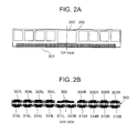
- FIGS. 2A and 2B are diagrams for explaining a schematic configuration of a memory board to which the present invention is applied, FIG. 2A being a top view and FIG. 2B being a side view of the memory board;
- FIG. 3 shows address signal waveforms observed when employing an address line topology of a memory module in a related art
- FIG. 4 is diagrams for explaining analysis of noise factors
- FIG. 5 is diagrams for explaining analysis of noise factors
- FIG. 6 shows address signal waveforms according to the first embodiment of the present invention
- FIG. 7 shows address signal waveforms according to the first embodiment of the present invention
- FIG. 8 is diagrams showing noise evaluation results of the address signal waveforms according to the first embodiment of the present invention.
- FIGS. 9A and 9B are diagrams showing address signal waveforms of memory elements in association with wiring lengths according to a second embodiment of the present invention, FIG. 9A showing the address signal waveforms and FIG. 9B showing the wiring lengths;
- FIG. 10A shows a stacked package structure
- FIG. 10B is a diagram showing a stacked package wiring configuration according a related art example
- FIG. 10C is a diagram showing a package wiring configuration according to a third embodiment of the present invention
- FIG. 11 shows address signal waveforms according to the third embodiment of the present invention.
- FIG. 12A shows address signal waveforms of memory elements while FIG. 12B shows wiring lengths according to the third embodiment of the present invention
- FIG. 13 is a diagram showing an example of configuration of a server device having a memory board according to a fourth embodiment of the present invention.
- FIG. 14 is a block diagram showing architecture of elements of the memory according to the fourth embodiment of the present invention.
- FIGS. 1 to 10 A first embodiment of the present invention will be described with reference to FIGS. 1 to 10 .
- the first embodiment is an example in which the present invention is applied to a buffered DIMM (Dual Inline Memory Module) comprising buffer elements (buffer circuits) mounted on a memory board as shown in FIGS. 2A and 2B .
- DIMM Dual Inline Memory Module
- FIG. 2A a DIMM board (memory board) 300 is electrically connected to a CPU board (not shown) through a connector terminal 301 , so that address signals and data signals for memory elements are transferred between a buffer element (data transfer element) 302 and a memory controller on the CPU board.
- the buffer element 302 transmits address and data signals to eighteen memory elements 304 R, 305 R, 306 R, 307 R, 313 R, 314 R, 315 R, 316 R, 317 R, 304 L, 305 L, 306 L, 307 L, 313 L, 314 L, 315 L, 316 L and 317 L.
- Each of the memory elements has a two-layer stacked structure in which two memory chips are mounted while being stacked on each other.
- FIG. 1A shows a topology of address signals between the buffer element 302 and the plurality of memory elements shown in FIG. 2B .
- the memory elements transmitting signals are divided into two systems, i.e., a right system (indicated by a suffix of R) and a left system (indicated by a suffix of L), arranged on the opposite sides of the buffer element 302 shown in FIG. 2B .
- a right system indicated by a suffix of R
- L left system
- the main line 101 R is branched into branch lines to the respective memory elements and is connected to a terminating end 120 R at a terminating potential Vtt via a terminating resistor 122 R having a resistance value of 20 ⁇ .
- the memory element 317 R arranged on the rear side of the buffer element 302 in FIG. 2B is connected to the main line 101 R through a branch line connecting to a first branch point S 1 which is closest to the buffer element 302 .
- Two memory elements 304 R and 313 R are connected to a second branch point S 2 of the main line 101 R on the front and rear surfaces, respectively.
- two memory elements 305 R and 314 R are connected to a third branch point S 3 of the main line 101 R on the front and rear surfaces, respectively.
- Two memory elements 306 R and 315 R are connected to a fourth branch point S 4 on the front and rear surfaces, respectively.
- Two memory elements 307 R and 316 R are connected to a fifth branch point S 5 on the front and rear surfaces, respectively.
- FIG. 1B shows wiring lengths (distances) of respective interconnections in the memory module according to the first embodiment.
- a wiring length TL 0 between the buffer element 302 and the first branch point S 1 is set to 11.6 mm
- a wiring length TL 1 between the first and the second branch points S 1 and S 2 is set to 11.0 mm
- a wiring length TL 3 _ 1 between the second and the third branch points S 2 and S 3 is set to 30 mm so as to establish relations of TL 0 ⁇ TL 1 , TL 0 ⁇ TL 3 _ 1 , and TL 1 ⁇ TL 3 _ 1 .
- the symbol “ ⁇ ” means that the wiring length TL 0 is substantially equal to the wiring length TL 1 .
- the wiring length TL 3 _ 2 between the third and the fourth branch points S 3 and S 4 and the wiring length TL 3 _ 2 between the fourth and the fifth branch points S 4 and S 5 are set to 15 mm so as to achieve the shortest interconnection.
- FIG. 1C shows wiring lengths of a wiring pattern in a related art.
- a wiring length TL 3 _ 1 between the second and the third branch points S 2 and S 3 a wiring length TL 3 _ 2 between the third and the fourth branch points S 3 and S 4 , and a wiring length TL 3 _ 2 between the fourth and the fifth branch points S 4 and S 5 are all set to 15 mm.
- Address signal waveforms under this condition were simulated and analyzed by using SPICE (Simulation Program for Integrated Circuit Evaluation). The analysis was conducted by transmitting a 533 MHz random signal from the buffer element 302 and signal waveforms observed at the input of each memory chip were represented in eye patterns. The results of this simulation analysis are shown in FIG.
- the signal waveform (the upper diagram of FIG. 3 ) in the lower chip D 17 of the memory element 317 R closest to the buffer element presents a constriction distortion in the middle of the eye pattern aperture.
- the signal waveform (the lower diagram of FIG. 3 ) in the lower chip D 13 of the memory element 313 R mounted at the second closest position to the buffer element presents a step in a rising portion, causing a substantial delay in rising time ⁇ tr.
- FIG. 4 shows results of analysis of causes of the waveform distortion in the lower chip D 17 .
- FIG. 4 shows a step pulse waveform observed when the wiring length TL 1 between the first and the second branch points S 1 and S 2 is extremely increased from 11 mm to 300 mm.
- the time at which the waveform distortion b due to constriction appears is delayed as the overshoot in the portion a circled by the broken line in FIG. 4 is increased. This is because the time at which negative reflection occurring after the second branch point S 2 reaches the lower chip D 17 is delayed, and hence the time at which the waveform distortion b due to the constriction appears is delayed.
- the overshoot in the portion a is increased because negative reflected waves produced at the first branch point S 1 are further reflected negatively at the buffer element to become positive reflected waves appearing as an overshoot waveform.
- the negative reflected waves are negatively reflected at the buffer element because the output impedance of an address terminal of the buffer element is lower than the characteristic impedance of the address signal line.
- this overshoot is partially canceled with reflected waves after the second branch point S 2 , resulting in a waveform having a small overshoot as shown in FIG. 4 .
- the reflected waves at the branch points after the second branch point S 2 affect the constricted waveform of the lower chip D 17 .
- FIG. 5 shows results of the analysis of blunting in the rising waveform of the lower chip D 13 .
- the period of time is measured to be 220 ps from the start of the rising waveform to the point D at which the waveform commences to blunt. If it is assumed that the propagation time is 7 ps/mm, the length becomes 31.4 mm, corresponding to about twice the wiring length (TL 3 _ 1 ) of 15 mm between the second and the third branch points S 2 and S 3 . Therefore, simulation analysis was conducted while changing the wiring length between the second and the third branch points S 2 and S 3 from 15 mm to 50 mm.
- the wiring configuration is such that the relations of TL 0 ⁇ TL 1 , TL 0 ⁇ TL 3 _ 1 , and TL 1 ⁇ TL 3 _ 1 are established among the wiring lengths.
- the wiring length TL 0 between the buffer element and the first branch point S 1 is set to be substantially equal to the wiring length TL 1 between the first and the second branch points S 1 and S 2 , whereby in the signal waveform of the memory element 317 R, the negative reflected waves from the second branch point S 2 are canceled with the positive reflected waves obtained by the negative reflected waves from the first branch point S 1 being reflected at the buffer element.
- the wiring length TL 3 _ 1 between the second and the third branch points S 2 and S 3 is set to be greater than TL 0 or TL 1 to delay the occurrence of blunting in the signal rising waveform of the memory element 313 R so that the waveform is interfered with the positive reflected waves reflected at the buffer element. This makes it possible to cause the rising waveform to start blunting after the time point when the threshold voltage is exceeded and, at the same time, to reduce the effect of the blunting.
- FIG. 6 and FIG. 7 respectively show address signal waveforms of the lower chips D 17 and D 13 as observed when the wiring length TL 3 _ 1 is changed from 9 mm to 30 mm.
- FIG. 8 shows the results of noise evaluation based on the voltage ⁇ V at the pinched portion of the lower chip D 17 (the upper diagram of FIG. 8 ) and the rising time ⁇ tr of the lower chip D 13 (the lower diagram of FIG. 8 ). It can be seen from these results that both the noise voltage ⁇ V of the lower chip D 17 and the rising time ⁇ tr of the lower chip D 13 can be reduced if the wiring length TL 3 _ 1 is 30 mm.
- the time required to propagate a signal over a distance corresponding to twice the wiring length (distance) TL 3 _ 1 from the second branch point S 2 where the second branch line branches to the third branch point S 3 where the third branch line branches is represented by T 2-3
- the rising time required for the address signal level to exceed a threshold voltage used for distinguishing the “0” level and the “1” level of the memory element connected to the branch point where the second branch line branches is represented by ⁇ t 2 .
- the delay time of the rising time ⁇ tr can be reduced if the wiring length TL 3 _ 1 is set to 24 mm or greater so that the signal propagation time T 2-3 is longer than the rising time ⁇ t 2 .
- the waveform distortion in the memory elements near the buffer element can be reduced by setting the wiring lengths in the wiring configuration shown in FIG. 1A to establish the relations of TL 0 ⁇ TL 1 , TL 0 ⁇ TL 3 _ 1 , and TL 1 ⁇ TL 3 _ 1 .
- FIG. 9A A second embodiment of the present invention will be described with reference to FIG. 1A and FIGS. 9A and 9B .
- the topology in FIG. 1A has a wiring configuration shown in FIG. 9B .
- the wiring lengths are such that TL 0 >TL 1 , TL 0 ⁇ TL 3 _ 1 , and TL 1 ⁇ TL 3 _ 1 .
- this wiring configuration also can minimize the waveform distortion in the memory elements.
- the wiring length TL 0 is set to be greater than the wiring length TL 1 , whereby the positive reflected waves obtained by reflecting reflected waves from the first branch point S 1 at the buffer element reaches after reaching of the negative reflected waves from the second branch point S 2 .
- This makes it possible to correct the waveform with the positive reflected waves from the buffer element, immediately after the occurrence of waveform distortion at the second branch point S 2 , and thus to reduce the waveform distortion and delay due to noise.
- FIG. 10A a memory package is formed by stacking the memory elements while equally setting the wiring lengths in the package.
- the wiring pattern on the printed wiring board is formed under the conditions shown in FIGS. 1A and 1B .
- wiring is branched into an upper memory chip and a lower memory chip at a solder ball for electrically connecting the package to a printed wiring board. Therefore, as shown in FIG. 10B , the wiring length to the upper memory chip is different from that to the lower memory chip.
- wiring from a solder ball for electrically connecting the package to a printed wiring board is branched in the vicinity of a solder ball for connecting an interposer for the upper chip and an interposer for the lower chip.
- the wiring length in the upper chip and the wiring length in the lower chip after the branching are substantially equal to each other.
- FIG. 11 and FIG. 12 show waveforms in the memory chip D 17 according to the third embodiment.
- the step in the rising waveform in the memory chip D 17 can be eliminated. This makes it possible not only to correct the waveform distortion due to reflection by the printed board but also to shape the waveform in the chip. Accordingly, a signal can be transmitted at a higher speed.
- FIGS. 13 and 14 A fourth embodiment of the present invention will be described with reference to FIGS. 13 and 14 .
- the memory board (memory DIMM board) 300 of the first embodiment (indicated by the reference number 1530 in FIG. 13 ) is mounted in a server device (information processing device) 1510 .
- the server device 1510 comprises a CPU board 1520 on which a CPU 1522 and a memory controller 1524 are mounted.
- the CPU board 1520 comprises a memory board 1530 according to the fourth embodiment mounted thereon.
- FIG. 14 is a block diagram showing architecture of elements of the memory of the server device according to the fourth embodiment.
- the server device comprising the memory board of the present invention mounted thereon is allowed to be mounted with a large-capacity and high-speed memory and thus to improve the throughput performance of the system as a whole.
- the present invention is generally applicable to semiconductor devices and printed wiring boards for mounting semiconductor devices.
Landscapes
- Engineering & Computer Science (AREA)
- Microelectronics & Electronic Packaging (AREA)
- Structure Of Printed Boards (AREA)
- Memory System (AREA)
Abstract
Description
Claims (16)
Priority Applications (1)
| Application Number | Priority Date | Filing Date | Title |
|---|---|---|---|
| US13/363,396 US8922029B2 (en) | 2007-09-28 | 2012-02-01 | Apparatus having a wiring board and memory devices |
Applications Claiming Priority (4)
| Application Number | Priority Date | Filing Date | Title |
|---|---|---|---|
| JP2007-253470 | 2007-09-28 | ||
| JP2007253470A JP5696301B2 (en) | 2007-09-28 | 2007-09-28 | Address line wiring structure and printed wiring board having the same |
| US12/239,900 US8134239B2 (en) | 2007-09-28 | 2008-09-29 | Address line wiring structure and printed wiring board having same |
| US13/363,396 US8922029B2 (en) | 2007-09-28 | 2012-02-01 | Apparatus having a wiring board and memory devices |
Related Parent Applications (1)
| Application Number | Title | Priority Date | Filing Date |
|---|---|---|---|
| US12/239,900 Continuation US8134239B2 (en) | 2007-09-28 | 2008-09-29 | Address line wiring structure and printed wiring board having same |
Publications (2)
| Publication Number | Publication Date |
|---|---|
| US20120127675A1 US20120127675A1 (en) | 2012-05-24 |
| US8922029B2 true US8922029B2 (en) | 2014-12-30 |
Family
ID=40508091
Family Applications (2)
| Application Number | Title | Priority Date | Filing Date |
|---|---|---|---|
| US12/239,900 Active 2030-07-17 US8134239B2 (en) | 2007-09-28 | 2008-09-29 | Address line wiring structure and printed wiring board having same |
| US13/363,396 Active US8922029B2 (en) | 2007-09-28 | 2012-02-01 | Apparatus having a wiring board and memory devices |
Family Applications Before (1)
| Application Number | Title | Priority Date | Filing Date |
|---|---|---|---|
| US12/239,900 Active 2030-07-17 US8134239B2 (en) | 2007-09-28 | 2008-09-29 | Address line wiring structure and printed wiring board having same |
Country Status (2)
| Country | Link |
|---|---|
| US (2) | US8134239B2 (en) |
| JP (1) | JP5696301B2 (en) |
Cited By (1)
| Publication number | Priority date | Publication date | Assignee | Title |
|---|---|---|---|---|
| US20140226278A1 (en) * | 2013-02-13 | 2014-08-14 | Canon Kabushiki Kaisha | Printed circuit board and printed wiring board |
Families Citing this family (13)
| Publication number | Priority date | Publication date | Assignee | Title |
|---|---|---|---|---|
| JP5696301B2 (en) * | 2007-09-28 | 2015-04-08 | ピーエスフォー ルクスコ エスエイアールエルPS4 Luxco S.a.r.l. | Address line wiring structure and printed wiring board having the same |
| JP5716604B2 (en) * | 2011-08-08 | 2015-05-13 | 富士通株式会社 | Circuit simulator program, apparatus, and eye pattern generation method |
| US9082464B2 (en) | 2012-02-14 | 2015-07-14 | Samsung Electronics Co., Ltd. | Memory module for high-speed operations |
| US9412423B2 (en) * | 2012-03-15 | 2016-08-09 | Samsung Electronics Co., Ltd. | Memory modules including plural memory devices arranged in rows and module resistor units |
| JP5930887B2 (en) * | 2012-07-05 | 2016-06-08 | 株式会社日立製作所 | Signal transmission circuit |
| KR20140121181A (en) | 2013-04-05 | 2014-10-15 | 삼성전자주식회사 | Printed circuit board and memory module including the same |
| US9361254B2 (en) * | 2013-08-09 | 2016-06-07 | Nvidia Corporation | Memory device formed with a semiconductor interposer |
| JP5925352B2 (en) | 2014-04-14 | 2016-05-25 | キヤノン株式会社 | Printed circuit board and printed wiring board |
| JP2016029785A (en) * | 2014-07-18 | 2016-03-03 | 株式会社東芝 | Communication system |
| US9980366B2 (en) | 2015-01-12 | 2018-05-22 | Qualcomm Incorporated | High speed signal routing topology for better signal quality |
| KR102596491B1 (en) | 2016-12-13 | 2023-10-30 | 삼성전자주식회사 | Semiconductor device |
| KR102640968B1 (en) * | 2018-05-29 | 2024-02-27 | 삼성전자주식회사 | Printed circuit board, storage device, and storage device including printed circuit board |
| JP7469978B2 (en) | 2020-07-22 | 2024-04-17 | 株式会社日立製作所 | Printed wiring board and information processing device |
Citations (17)
| Publication number | Priority date | Publication date | Assignee | Title |
|---|---|---|---|---|
| US5394121A (en) | 1993-10-15 | 1995-02-28 | International Business Machines Corporation | Wiring topology for transfer of electrical signals |
| JPH07250104A (en) | 1994-03-08 | 1995-09-26 | Hitachi Ltd | Signal transmission circuit |
| US6125419A (en) | 1996-06-13 | 2000-09-26 | Hitachi, Ltd. | Bus system, printed circuit board, signal transmission line, series circuit and memory module |
| US20010045874A1 (en) * | 2000-05-04 | 2001-11-29 | Samsung Electronics Co., Ltd. | System board and impedance control method thereof |
| US20030037216A1 (en) | 2001-07-26 | 2003-02-20 | Kayoko Shibata | Memory module |
| JP2004062530A (en) | 2002-07-29 | 2004-02-26 | Elpida Memory Inc | Memory module and memory system |
| US20040251929A1 (en) | 2003-06-11 | 2004-12-16 | Pax George E. | Memory module and method having improved signal routing topology |
| US20050052912A1 (en) | 2003-09-04 | 2005-03-10 | Mike Cogdill | Circuit and system for addressing memory modules |
| US20050086418A1 (en) | 2003-09-04 | 2005-04-21 | Mike Cogdill | Circuit and system for accessing memory modules |
| US20050142950A1 (en) * | 2000-05-10 | 2005-06-30 | Rambus Inc. | Multiple channel modules and bus systems using same |
| US6927992B1 (en) | 2003-05-12 | 2005-08-09 | Pericom Semiconductor Corp. | Trace-impedance matching at junctions of multi-load signal traces to eliminate termination |
| US6978328B1 (en) | 1999-05-12 | 2005-12-20 | Hitachi, Ltd. | Bus system, memory system, printed circuit board and directional coupler |
| US20060236031A1 (en) * | 2001-02-28 | 2006-10-19 | Rambus Inc. | Upgradable memory system with reconfigurable interconnect |
| US20070194968A1 (en) | 2006-02-03 | 2007-08-23 | Samsung Electronics Co., Ltd. | Memory system including a power divider on a multi module memory bus |
| US7389381B1 (en) * | 2006-04-05 | 2008-06-17 | Co Ramon S | Branching memory-bus module with multiple downlink ports to standard fully-buffered memory modules |
| US7697332B2 (en) * | 2007-12-13 | 2010-04-13 | Alcatel Lucent | Placement and routing of ECC memory devices for improved signal timing |
| US8134239B2 (en) * | 2007-09-28 | 2012-03-13 | Elpida Memory, Inc. | Address line wiring structure and printed wiring board having same |
Family Cites Families (1)
| Publication number | Priority date | Publication date | Assignee | Title |
|---|---|---|---|---|
| JP3821678B2 (en) * | 2001-09-06 | 2006-09-13 | エルピーダメモリ株式会社 | Memory device |
-
2007
- 2007-09-28 JP JP2007253470A patent/JP5696301B2/en not_active Expired - Fee Related
-
2008
- 2008-09-29 US US12/239,900 patent/US8134239B2/en active Active
-
2012
- 2012-02-01 US US13/363,396 patent/US8922029B2/en active Active
Patent Citations (18)
| Publication number | Priority date | Publication date | Assignee | Title |
|---|---|---|---|---|
| US5394121A (en) | 1993-10-15 | 1995-02-28 | International Business Machines Corporation | Wiring topology for transfer of electrical signals |
| JPH07250104A (en) | 1994-03-08 | 1995-09-26 | Hitachi Ltd | Signal transmission circuit |
| US6125419A (en) | 1996-06-13 | 2000-09-26 | Hitachi, Ltd. | Bus system, printed circuit board, signal transmission line, series circuit and memory module |
| US6978328B1 (en) | 1999-05-12 | 2005-12-20 | Hitachi, Ltd. | Bus system, memory system, printed circuit board and directional coupler |
| US20010045874A1 (en) * | 2000-05-04 | 2001-11-29 | Samsung Electronics Co., Ltd. | System board and impedance control method thereof |
| US20050142950A1 (en) * | 2000-05-10 | 2005-06-30 | Rambus Inc. | Multiple channel modules and bus systems using same |
| US20060236031A1 (en) * | 2001-02-28 | 2006-10-19 | Rambus Inc. | Upgradable memory system with reconfigurable interconnect |
| US20030037216A1 (en) | 2001-07-26 | 2003-02-20 | Kayoko Shibata | Memory module |
| JP2004062530A (en) | 2002-07-29 | 2004-02-26 | Elpida Memory Inc | Memory module and memory system |
| US6927992B1 (en) | 2003-05-12 | 2005-08-09 | Pericom Semiconductor Corp. | Trace-impedance matching at junctions of multi-load signal traces to eliminate termination |
| US20040251929A1 (en) | 2003-06-11 | 2004-12-16 | Pax George E. | Memory module and method having improved signal routing topology |
| US20050086418A1 (en) | 2003-09-04 | 2005-04-21 | Mike Cogdill | Circuit and system for accessing memory modules |
| US20050052912A1 (en) | 2003-09-04 | 2005-03-10 | Mike Cogdill | Circuit and system for addressing memory modules |
| US20070194968A1 (en) | 2006-02-03 | 2007-08-23 | Samsung Electronics Co., Ltd. | Memory system including a power divider on a multi module memory bus |
| US7389381B1 (en) * | 2006-04-05 | 2008-06-17 | Co Ramon S | Branching memory-bus module with multiple downlink ports to standard fully-buffered memory modules |
| US7904655B2 (en) * | 2006-04-05 | 2011-03-08 | Co Ramon S | Branching memory-bus module with multiple downlink ports to standard fully-buffered memory modules |
| US8134239B2 (en) * | 2007-09-28 | 2012-03-13 | Elpida Memory, Inc. | Address line wiring structure and printed wiring board having same |
| US7697332B2 (en) * | 2007-12-13 | 2010-04-13 | Alcatel Lucent | Placement and routing of ECC memory devices for improved signal timing |
Cited By (2)
| Publication number | Priority date | Publication date | Assignee | Title |
|---|---|---|---|---|
| US20140226278A1 (en) * | 2013-02-13 | 2014-08-14 | Canon Kabushiki Kaisha | Printed circuit board and printed wiring board |
| US9456489B2 (en) * | 2013-02-13 | 2016-09-27 | Canon Kabushiki Kaisha | Printed circuit board and printed wiring board |
Also Published As
| Publication number | Publication date |
|---|---|
| JP2009086841A (en) | 2009-04-23 |
| US20120127675A1 (en) | 2012-05-24 |
| US20090086522A1 (en) | 2009-04-02 |
| US8134239B2 (en) | 2012-03-13 |
| JP5696301B2 (en) | 2015-04-08 |
Similar Documents
| Publication | Publication Date | Title |
|---|---|---|
| US8922029B2 (en) | Apparatus having a wiring board and memory devices | |
| KR100691583B1 (en) | Multi-drop bus structure memory system with multiple termination resistors | |
| US7205789B1 (en) | Termination arrangement for high speed data rate multi-drop data bit connections | |
| KR100348726B1 (en) | Directional coupling memory module | |
| US6937494B2 (en) | Memory module, memory chip, and memory system | |
| KR100689967B1 (en) | Memory system with improved multi-module memory bus structure | |
| US8866282B2 (en) | Semiconductor apparatus, signal transmission system and signal transmission method | |
| US8195855B2 (en) | Bi-directional multi-drop bus memory system | |
| US8036011B2 (en) | Memory module for improving signal integrity and computer system having the same | |
| US6930904B2 (en) | Circuit topology for high-speed memory access | |
| US7194572B2 (en) | Memory system and method to reduce reflection and signal degradation | |
| JPH1027049A (en) | Interconnected bus | |
| US6335955B1 (en) | Connection, system and method of phase delayed synchronization in high speed digital systems using delay elements | |
| US7133962B2 (en) | Circulator chain memory command and address bus topology | |
| US9767859B2 (en) | Printed circuit board and printed wiring board | |
| US5394121A (en) | Wiring topology for transfer of electrical signals | |
| US7254675B2 (en) | Memory system having memory modules with different memory device loads | |
| KR100355714B1 (en) | Digital Information Processing System With A Modular Bus Architecture | |
| CN100445974C (en) | High Speed Signal Transmission Device | |
| Park et al. | Advanced Fly-By Routing Topology for Gbps DDR5 Systems | |
| JP4912830B2 (en) | Transmission device, and flip chip and module using the same | |
| TWI294259B (en) | Interconnection t type topology of transmission line | |
| JP2001344299A (en) | Wiring structure having branch point and method for forming wiring constitution having branch point |
Legal Events
| Date | Code | Title | Description |
|---|---|---|---|
| AS | Assignment |
Owner name: ELPIDA MEMORY, INC., JAPAN Free format text: ASSIGNMENT OF ASSIGNORS INTEREST;ASSIGNORS:HIRAISHI, ATSUSHI;SUGANO, TOSHIO;YAMAGUCHI, MASAHIRO;AND OTHERS;REEL/FRAME:027629/0534 Effective date: 20081125 |
|
| AS | Assignment |
Owner name: ELPIDA MEMORY INC., JAPAN Free format text: SECURITY AGREEMENT;ASSIGNOR:PS4 LUXCO S.A.R.L.;REEL/FRAME:032414/0261 Effective date: 20130726 |
|
| AS | Assignment |
Owner name: PS4 LUXCO S.A.R.L., LUXEMBOURG Free format text: ASSIGNMENT OF ASSIGNORS INTEREST;ASSIGNOR:ELPIDA MEMORY, INC.;REEL/FRAME:032897/0575 Effective date: 20130726 |
|
| FEPP | Fee payment procedure |
Free format text: PAYOR NUMBER ASSIGNED (ORIGINAL EVENT CODE: ASPN); ENTITY STATUS OF PATENT OWNER: LARGE ENTITY |
|
| STCF | Information on status: patent grant |
Free format text: PATENTED CASE |
|
| AS | Assignment |
Owner name: PS5 LUXCO S.A.R.L., LUXEMBOURG Free format text: ASSIGNMENT OF ASSIGNORS INTEREST;ASSIGNOR:PS4 LUXCO S.A.R.L.;REEL/FRAME:039818/0506 Effective date: 20130829 Owner name: LONGITUDE SEMICONDUCTOR S.A.R.L., LUXEMBOURG Free format text: CHANGE OF NAME;ASSIGNOR:PS5 LUXCO S.A.R.L.;REEL/FRAME:039793/0880 Effective date: 20131112 |
|
| MAFP | Maintenance fee payment |
Free format text: PAYMENT OF MAINTENANCE FEE, 4TH YEAR, LARGE ENTITY (ORIGINAL EVENT CODE: M1551) Year of fee payment: 4 |
|
| AS | Assignment |
Owner name: LONGITUDE LICENSING LIMITED, IRELAND Free format text: ASSIGNMENT OF ASSIGNORS INTEREST;ASSIGNOR:LONGITUDE SEMICONDUCTOR S.A.R.L.;REEL/FRAME:046865/0667 Effective date: 20180731 |
|
| MAFP | Maintenance fee payment |
Free format text: PAYMENT OF MAINTENANCE FEE, 8TH YEAR, LARGE ENTITY (ORIGINAL EVENT CODE: M1552); ENTITY STATUS OF PATENT OWNER: LARGE ENTITY Year of fee payment: 8 |