US8921237B2 - Method of depositing a film - Google Patents
Method of depositing a film Download PDFInfo
- Publication number
- US8921237B2 US8921237B2 US14/134,065 US201314134065A US8921237B2 US 8921237 B2 US8921237 B2 US 8921237B2 US 201314134065 A US201314134065 A US 201314134065A US 8921237 B2 US8921237 B2 US 8921237B2
- Authority
- US
- United States
- Prior art keywords
- film
- turntable
- depositing
- wafer
- gas
- Prior art date
- Legal status (The legal status is an assumption and is not a legal conclusion. Google has not performed a legal analysis and makes no representation as to the accuracy of the status listed.)
- Active
Links
Images







Classifications
-
- H—ELECTRICITY
- H10—SEMICONDUCTOR DEVICES; ELECTRIC SOLID-STATE DEVICES NOT OTHERWISE PROVIDED FOR
- H10P—GENERIC PROCESSES OR APPARATUS FOR THE MANUFACTURE OR TREATMENT OF DEVICES COVERED BY CLASS H10
- H10P14/00—Formation of materials, e.g. in the shape of layers or pillars
- H10P14/60—Formation of materials, e.g. in the shape of layers or pillars of insulating materials
- H10P14/63—Formation of materials, e.g. in the shape of layers or pillars of insulating materials characterised by the formation processes
- H10P14/6326—Deposition processes
- H10P14/6328—Deposition from the gas or vapour phase
- H10P14/6334—Deposition from the gas or vapour phase using decomposition or reaction of gaseous or vapour phase compounds, i.e. chemical vapour deposition
- H10P14/6339—Deposition from the gas or vapour phase using decomposition or reaction of gaseous or vapour phase compounds, i.e. chemical vapour deposition deposition by cyclic CVD, e.g. ALD, ALE or pulsed CVD
-
- H01L21/0228—
-
- C—CHEMISTRY; METALLURGY
- C23—COATING METALLIC MATERIAL; COATING MATERIAL WITH METALLIC MATERIAL; CHEMICAL SURFACE TREATMENT; DIFFUSION TREATMENT OF METALLIC MATERIAL; COATING BY VACUUM EVAPORATION, BY SPUTTERING, BY ION IMPLANTATION OR BY CHEMICAL VAPOUR DEPOSITION, IN GENERAL; INHIBITING CORROSION OF METALLIC MATERIAL OR INCRUSTATION IN GENERAL
- C23C—COATING METALLIC MATERIAL; COATING MATERIAL WITH METALLIC MATERIAL; SURFACE TREATMENT OF METALLIC MATERIAL BY DIFFUSION INTO THE SURFACE, BY CHEMICAL CONVERSION OR SUBSTITUTION; COATING BY VACUUM EVAPORATION, BY SPUTTERING, BY ION IMPLANTATION OR BY CHEMICAL VAPOUR DEPOSITION, IN GENERAL
- C23C16/00—Chemical coating by decomposition of gaseous compounds, without leaving reaction products of surface material in the coating, i.e. chemical vapour deposition [CVD] processes
- C23C16/22—Chemical coating by decomposition of gaseous compounds, without leaving reaction products of surface material in the coating, i.e. chemical vapour deposition [CVD] processes characterised by the deposition of inorganic material, other than metallic material
- C23C16/30—Deposition of compounds, mixtures or solid solutions, e.g. borides, carbides, nitrides
- C23C16/34—Nitrides
-
- C—CHEMISTRY; METALLURGY
- C23—COATING METALLIC MATERIAL; COATING MATERIAL WITH METALLIC MATERIAL; CHEMICAL SURFACE TREATMENT; DIFFUSION TREATMENT OF METALLIC MATERIAL; COATING BY VACUUM EVAPORATION, BY SPUTTERING, BY ION IMPLANTATION OR BY CHEMICAL VAPOUR DEPOSITION, IN GENERAL; INHIBITING CORROSION OF METALLIC MATERIAL OR INCRUSTATION IN GENERAL
- C23C—COATING METALLIC MATERIAL; COATING MATERIAL WITH METALLIC MATERIAL; SURFACE TREATMENT OF METALLIC MATERIAL BY DIFFUSION INTO THE SURFACE, BY CHEMICAL CONVERSION OR SUBSTITUTION; COATING BY VACUUM EVAPORATION, BY SPUTTERING, BY ION IMPLANTATION OR BY CHEMICAL VAPOUR DEPOSITION, IN GENERAL
- C23C16/00—Chemical coating by decomposition of gaseous compounds, without leaving reaction products of surface material in the coating, i.e. chemical vapour deposition [CVD] processes
- C23C16/44—Chemical coating by decomposition of gaseous compounds, without leaving reaction products of surface material in the coating, i.e. chemical vapour deposition [CVD] processes characterised by the method of coating
- C23C16/4401—Means for minimising impurities, e.g. dust, moisture or residual gas, in the reaction chamber
- C23C16/4404—Coatings or surface treatment on the inside of the reaction chamber or on parts thereof
-
- C—CHEMISTRY; METALLURGY
- C23—COATING METALLIC MATERIAL; COATING MATERIAL WITH METALLIC MATERIAL; CHEMICAL SURFACE TREATMENT; DIFFUSION TREATMENT OF METALLIC MATERIAL; COATING BY VACUUM EVAPORATION, BY SPUTTERING, BY ION IMPLANTATION OR BY CHEMICAL VAPOUR DEPOSITION, IN GENERAL; INHIBITING CORROSION OF METALLIC MATERIAL OR INCRUSTATION IN GENERAL
- C23C—COATING METALLIC MATERIAL; COATING MATERIAL WITH METALLIC MATERIAL; SURFACE TREATMENT OF METALLIC MATERIAL BY DIFFUSION INTO THE SURFACE, BY CHEMICAL CONVERSION OR SUBSTITUTION; COATING BY VACUUM EVAPORATION, BY SPUTTERING, BY ION IMPLANTATION OR BY CHEMICAL VAPOUR DEPOSITION, IN GENERAL
- C23C16/00—Chemical coating by decomposition of gaseous compounds, without leaving reaction products of surface material in the coating, i.e. chemical vapour deposition [CVD] processes
- C23C16/44—Chemical coating by decomposition of gaseous compounds, without leaving reaction products of surface material in the coating, i.e. chemical vapour deposition [CVD] processes characterised by the method of coating
- C23C16/455—Chemical coating by decomposition of gaseous compounds, without leaving reaction products of surface material in the coating, i.e. chemical vapour deposition [CVD] processes characterised by the method of coating characterised by the method used for introducing gases into reaction chamber or for modifying gas flows in reaction chamber
- C23C16/45523—Pulsed gas flow or change of composition over time
- C23C16/45525—Atomic layer deposition [ALD]
- C23C16/45544—Atomic layer deposition [ALD] characterized by the apparatus
- C23C16/45548—Atomic layer deposition [ALD] characterized by the apparatus having arrangements for gas injection at different locations of the reactor for each ALD half-reaction
- C23C16/45551—Atomic layer deposition [ALD] characterized by the apparatus having arrangements for gas injection at different locations of the reactor for each ALD half-reaction for relative movement of the substrate and the gas injectors or half-reaction reactor compartments
-
- H01L21/28556—
-
- H01L21/68764—
-
- H01L21/68771—
-
- H—ELECTRICITY
- H10—SEMICONDUCTOR DEVICES; ELECTRIC SOLID-STATE DEVICES NOT OTHERWISE PROVIDED FOR
- H10P—GENERIC PROCESSES OR APPARATUS FOR THE MANUFACTURE OR TREATMENT OF DEVICES COVERED BY CLASS H10
- H10P72/00—Handling or holding of wafers, substrates or devices during manufacture or treatment thereof
- H10P72/70—Handling or holding of wafers, substrates or devices during manufacture or treatment thereof for supporting or gripping
- H10P72/76—Handling or holding of wafers, substrates or devices during manufacture or treatment thereof for supporting or gripping using mechanical means, e.g. clamps or pinches
- H10P72/7604—Handling or holding of wafers, substrates or devices during manufacture or treatment thereof for supporting or gripping using mechanical means, e.g. clamps or pinches the wafers being placed on a susceptor, stage or support
- H10P72/7618—Handling or holding of wafers, substrates or devices during manufacture or treatment thereof for supporting or gripping using mechanical means, e.g. clamps or pinches the wafers being placed on a susceptor, stage or support characterised by a movable susceptor, stage or support, others than those only rotating on their own vertical axis, e.g. susceptors on a rotating carrousel
-
- H—ELECTRICITY
- H10—SEMICONDUCTOR DEVICES; ELECTRIC SOLID-STATE DEVICES NOT OTHERWISE PROVIDED FOR
- H10P—GENERIC PROCESSES OR APPARATUS FOR THE MANUFACTURE OR TREATMENT OF DEVICES COVERED BY CLASS H10
- H10P72/00—Handling or holding of wafers, substrates or devices during manufacture or treatment thereof
- H10P72/70—Handling or holding of wafers, substrates or devices during manufacture or treatment thereof for supporting or gripping
- H10P72/76—Handling or holding of wafers, substrates or devices during manufacture or treatment thereof for supporting or gripping using mechanical means, e.g. clamps or pinches
- H10P72/7604—Handling or holding of wafers, substrates or devices during manufacture or treatment thereof for supporting or gripping using mechanical means, e.g. clamps or pinches the wafers being placed on a susceptor, stage or support
- H10P72/7621—Handling or holding of wafers, substrates or devices during manufacture or treatment thereof for supporting or gripping using mechanical means, e.g. clamps or pinches the wafers being placed on a susceptor, stage or support characterised by supporting two or more semiconductor substrates
-
- H—ELECTRICITY
- H10—SEMICONDUCTOR DEVICES; ELECTRIC SOLID-STATE DEVICES NOT OTHERWISE PROVIDED FOR
- H10P—GENERIC PROCESSES OR APPARATUS FOR THE MANUFACTURE OR TREATMENT OF DEVICES COVERED BY CLASS H10
- H10P14/00—Formation of materials, e.g. in the shape of layers or pillars
- H10P14/40—Formation of materials, e.g. in the shape of layers or pillars of conductive or resistive materials
- H10P14/412—Deposition of metallic or metal-silicide materials
-
- H—ELECTRICITY
- H10—SEMICONDUCTOR DEVICES; ELECTRIC SOLID-STATE DEVICES NOT OTHERWISE PROVIDED FOR
- H10P—GENERIC PROCESSES OR APPARATUS FOR THE MANUFACTURE OR TREATMENT OF DEVICES COVERED BY CLASS H10
- H10P14/00—Formation of materials, e.g. in the shape of layers or pillars
- H10P14/40—Formation of materials, e.g. in the shape of layers or pillars of conductive or resistive materials
- H10P14/42—Formation of materials, e.g. in the shape of layers or pillars of conductive or resistive materials using a gas or vapour
- H10P14/43—Chemical deposition, e.g. chemical vapour deposition [CVD]
-
- H—ELECTRICITY
- H10—SEMICONDUCTOR DEVICES; ELECTRIC SOLID-STATE DEVICES NOT OTHERWISE PROVIDED FOR
- H10W—GENERIC PACKAGES, INTERCONNECTIONS, CONNECTORS OR OTHER CONSTRUCTIONAL DETAILS OF DEVICES COVERED BY CLASS H10
- H10W20/00—Interconnections in chips, wafers or substrates
- H10W20/01—Manufacture or treatment
- H10W20/031—Manufacture or treatment of conductive parts of the interconnections
- H10W20/032—Manufacture or treatment of conductive parts of the interconnections of conductive barrier, adhesion or liner layers
Definitions
- the present invention relates to a method of depositing a film.
- a manufacturing process of a semiconductor integrated circuit includes a process of forming a thin film on a semiconductor wafer. In this process, improvement in evenness of a surface of a wafer is required in view of further microminiaturization of an IC.
- a method of depositing a film to satisfy this requirement a method of depositing the film called an atomic layer deposition (ALD) method or a molecular layer deposition (MLD) method is considered.
- ALD atomic layer deposition
- MLD molecular layer deposition
- the ALD method a cycle in which one (a reaction gas A) of two types of reaction gases, which mutually react, is caused to adsorb on the surface of the wafer, and the adsorbing reaction gas A is reacted with the other one (a reaction gas B) of the two types of reaction gases is repeated thereby depositing a thin film made of a reaction product onto the surface of the wafer. Because the ALD method uses the adsorption of the reaction gas onto the surface of the wafer, the ALD method has an advantage that film thickness evenness and film thickness controllability are excellent.
- a turntable-type film deposition apparatus is disclosed in Japanese Patent No. 4661990 as a film deposition apparatus performing the ALD method.
- This film deposition apparatus includes a turntable, which is rotatable and is positioned in a vacuum chamber, and on which a plurality of wafers are mounted, a separating area that is laid out above the turntable and separates a gas supplying area for the reaction gas A from a gas supplying area for the reaction gas B, evacuation ports corresponding to the gas supplying areas where the reaction gas A and the reaction gas B are supplied, and an evacuation device connected to these evacuation ports.
- the wafers pass through the gas supplying area for the reaction gas A, the separating area, the gas supplying area for the reaction gas B, and the separating area along rotation of the turntable.
- the reaction gas A adsorbs onto the surface of the wafer in the gas supplying area for the reaction gas A, and the reaction gas A reacts with the reaction gas B in the gas supplying area for the reaction gas B. Therefore, it is not necessary to change the reaction gas A to the reaction gas B while depositing the film, and the reaction gases A and B can be continuously supplied. Therefore, there is an advantage that an evacuation/purge process is unnecessary thereby shorting a time period for depositing the film.
- a capacitor using a high-dielectric material such as a metal oxide as a high-dielectric material is more frequently used.
- the electrodes of this capacitor are made from titanium nitride (TiN) having relatively great work function.
- the TiN electrodes are produced by depositing TiN onto a high dielectric layer by a chemical vapor deposition (CVD) method using titanium chloride (TiCl 4 ) and ammonia (NH 3 ) as raw gases and patterning the deposited TiN as disclosed, for example, Japanese Patent No. 4583764.
- CVD chemical vapor deposition
- the above film deposition apparatus of the turntable type is used to deposit a film by the ALD method, and it may be possible to deposit a film of titanium nitride by a process having excellent film thickness evenness and film thickness controllability and a shortened time period for depositing the film.
- embodiments of the present invention may provide a novel and useful method of depositing a film.
- a method of depositing a film using an atomic layer deposition (ALD) method while rotating a turntable provided inside a chamber and including a substrate mounting portion, onto which a substrate can be mounted, to cause the substrate to pass through first and second process areas, into which different gases to be mutually reacted are respectively supplied including coating the turntable with the film under a state where the wafer is not mounted onto the turntable, the turntable is rotated, and the substrate mounting portion has a predetermined temperature; and processing to deposit the film on the wafer under a state where the wafer is mounted onto the turntable, the turntable is rotated, and the substrate has a temperature equal to or less than the predetermined temperature.
- ALD atomic layer deposition
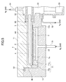
- FIG. 1 is a cross-sectional view for illustrating a film deposition apparatus preferable for performing a method of depositing a film of an embodiment of the present invention
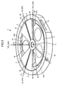
- FIG. 2 is a perspective view for illustrating a film deposition apparatus preferable for performing the method of depositing the film of the embodiment of the present invention
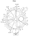
- FIG. 3 is a plan view for illustrating the film deposition apparatus preferable for performing the method of depositing the film of the embodiment of the present invention
- FIG. 4 is a cross-sectional view of a chamber along a concentric circle of an exemplary turntable of the film deposition apparatus preferable for performing the method of depositing the film of the embodiment of the present invention
- FIG. 5 is a cross-sectional view for illustrating the film deposition apparatus preferable for performing the method of depositing the film of the embodiment of the present invention
- FIG. 6 is a flow chart of the method of depositing the film of the embodiment of the present invention.
- FIG. 7 illustrates a result of performing a method of depositing a film of a comparative example using the film deposition apparatus of the embodiment of the present invention
- FIG. 8 illustrates a change of characteristics of the TiN film in high-temperature film deposition
- FIG. 9 illustrates a relationship between a wafer temperature in a process of depositing a film and a film density
- FIG. 10 illustrates a relationship between a wafer temperature in a process of depositing a film and a chloride concentration
- FIG. 11A illustrates an exemplary cross-sectional structure of a film having a great particle size obtained in a process of depositing the film under a high temperature condition in order to explain a principle of preventing metallic contamination using the film having the great particle size;
- FIG. 11B illustrates an exemplary cross-sectional structure of a film having a small particle size
- FIG. 12 illustrates a result of performing the method of depositing the film of a first embodiment
- FIG. 13 illustrates a result of performing the method of depositing the film of a second embodiment.
- FIG. 1 is a cross-sectional view of an exemplary film deposition apparatus preferable for performing a method of depositing a film of an embodiment of the present invention.
- FIG. 2 is a perspective view of the exemplary film deposition apparatus suitable for performing the method of depositing the film of the embodiment.
- FIG. 3 is a plan view for illustrating the film deposition apparatus preferable for performing the method of depositing the film of the embodiment of the present invention.
- the film deposition apparatus of the embodiment includes a chamber 1 having a substantially circular shape in its plan view and a flattened shape in its side view, and a turntable 2 having its rotational center in the center of the chamber 1 .
- the chamber 1 includes a chamber body 12 having a bottomed cylindrical shape, and a ceiling plate 11 , which is detachably provided onto the upper surface of the chamber body 12 through a sealing member 13 (see FIG. 1 ) such as an O-ring to hermetically seal the chamber 1 .
- the chamber 1 may be made of various material, for example, aluminum (Al).
- Al aluminum
- a screw made of stainless steel is used to assemble the chamber 1 .
- the screw may contain various metals such as copper (Cu).
- Cu copper
- Cu copper
- the inside of the chamber 1 is heated in a film deposition process, copper may separate out as an impurity from the screw.
- production of metallic contaminant is effectively prevented. A specific content of the method of depositing the film will be described in detail later.
- the turntable 2 is fixed by a core portion 21 in a cylindrical shape at the center portion of the turntable 2 .
- the core unit 21 is fixed to the upper end of a rotational shaft 22 extending in the vertical direction.
- the rotational shaft 22 penetrates through a bottom portion 14 of the chamber 1 .
- the lower end of the rotational shaft 22 is attached to a driving mechanism 23 , which causes the rotational shaft 22 (see FIG. 1 ) to rotate around the vertical axis of the rotational shaft 22 .
- the rotational shaft 22 and the driving mechanism 23 are accommodated in a cylindrical case body 20 whose upper surface is opened.
- a flange on the upper surface of the case body 20 is hermetically attached to the lower surface of a bottom portion 14 of the chamber 1 to maintain a gastight state between the inner atmosphere and the outer atmosphere of the case body 20 .
- FIG. 3 illustrates a state where the wafer W is mounted in only one circular concave portion 24 for convenience.
- the inner diameter of the circular concave portion 24 is slightly greater than the diameter of the wafer W by, for example, 4 mm.
- the depth of the circular concave portion 24 is substantially equal to the thickness of the wafer W.
- the height of the surface of the wafer W is substantially the same as the height of the surface of the turntable in an area where the wafer is not mounted.
- Through holes (not illustrated), through which lift pins for lifting up and down the back surfaces of the wafers W by supporting the back surfaces, penetrate through the bottom surfaces of the circular concave portions 24 .
- the number of the lift pins is three.
- the turntable 2 may be made of various material, and may be made of, for example, quartz. There may be a case where quartz may contain stainless steel as an impurity, and such stainless steel may contain a metallic impurity such as copper. Although such metallic impurity may be produced as metallic contaminant when the turntable 2 is heated at a high temperature, such metallic impurity prevents metallic contaminant from being produced by the method of depositing the film of the embodiment. A specific content of the method of depositing the film will be described in detail later.
- FIGS. 2 and 3 illustrate the structure inside the chamber 1 .
- the ceiling plate 11 is omitted from illustration in FIGS. 2 and 3 .
- a reaction gas nozzle 31 As illustrated in FIGS. 2 and 3 , a reaction gas nozzle 31 , a reaction gas nozzle 32 , and separation gas nozzles 41 , 42 , which are made of, for example, quartz, are arranged above the turntable 2 while interposing gaps in a peripheral direction of the chamber 1 (a rotational direction along an arrow A in FIG. 3 of the turntable 2 ).
- a reaction gas nozzle 31 As illustrated in FIGS. 2 and 3 , a reaction gas nozzle 31 , a reaction gas nozzle 32 , and separation gas nozzles 41 , 42 , which are made of, for example, quartz, are arranged above the turntable 2 while interposing gaps in a peripheral direction of the chamber 1 (a rotational direction along an arrow A in FIG. 3 of the turntable 2 ).
- the separation gas nozzle 41 , the reaction gas nozzle 31 , the separation gas nozzle 42 , and the reaction gas nozzle 32 are arranged in this order in a clockwise direction (the rotational direction of the turntable 2 ) from a transfer opening 15 described below.
- These nozzles 31 , 32 , 41 , and 42 are attached to the chamber body 12 by fixing gas introducing ports 31 a , 32 a , 41 a , and 42 a (see FIG. 3 ), which are base portions of the nozzles 31 , 41 , and 42 , respectively, to the outer peripheral wall of the chamber 1 so as to horizontally extend along radii of the chamber body 12 .
- these nozzles 31 , 32 , 41 , and 42 are introduced inside the chamber 1 from the outer peripheral wall of the chamber 12 .
- the reaction gas nozzle 31 is connected to a supplying source (not illustrated) of a titanium chloride (TiCl 4 ) gas through a pipe arrangement, a flow controller, or the like (not illustrated).
- the reaction gas nozzle 32 is connected to a supplying source (not illustrated) of ammonia through a pipe arrangement, a flow controller, or the like (not illustrated).
- the separation gas nozzles 41 and 42 are connected to a supplying source (not illustrated) of a separation gas through a pipe arrangement, a flow controller, or the like (not illustrated).
- the separation gas may be an inert gas such as a rare gas of helium (He), Argon (Ar) or the like or a nitrogen (N 2 ) gas. Within the embodiment, the N 2 gas is used.
- a plurality of gas ejection holes 33 opening toward the turntable 2 are arranged in the reaction gas nozzles 31 and 32 along the longitudinal directions of the reaction gas nozzles 31 and 32 at an interval of, for example, 10 mm.
- a first process area P 1 used to cause a TiClH 4 gas to adsorb onto the wafer W.
- the lower area of the reaction gas nozzle 32 is a second process area P 2 where the TiClH 4 gas adsorbing onto the wafer W in the first process area P 1 is nitrided.
- each convex portion 4 has a substantially sector form in its plan view with its apex cut in a circular arc shape.
- an inner circular arc is connected to a ring-shaped protruding portion (described later), and an outer circular arc is arranged along an inner peripheral surface of the chamber body 12 of the chamber 1 .
- FIG. 4 is a cross-sectional view of the chamber 1 along a concentric circle of the turntable 2 from the reaction gas nozzle 31 to the reaction gas nozzle 32 .
- a convex portion 4 is attached onto the back surface of the ceiling plate 11 .
- a high ceiling surface 45 (a second ceiling surface), which is a higher surface of the convex portion 4 and is positioned on both sides of the low ceiling surface 44 in a peripheral direction.
- the low ceiling surface 44 is shaped like a sector having an outer edge cut so as to form like a circular arc in its plan view. Further, as illustrated in FIG.
- a groove portion 43 is formed in a center of the convex portion 4 in its peripheral direction so as to extend in a radius direction.
- the separation gas nozzle 42 is accommodated inside the groove portion 43 .
- Another groove portion 43 is similarly formed in another convex portion 4 .
- the separation gas nozzle 41 is accommodated in the other groove portion 43 .
- the reaction gas nozzles 31 and 32 are provided in spaces lower than the high ceiling surface 45 .
- the reaction gas nozzles 31 and 32 are provided in the vicinity of the wafer W and apart from the ceiling surface 45 .
- the lower space of the ceiling surface 45 where the reaction gas nozzle 31 is provided is called a space 481
- the lower space of the ceiling surface 45 where the reaction gas nozzle 32 is provided is called a space 482 .
- a plurality of gas injection holes 42 h opening toward the turntable 2 are provided in the separation gas nozzle 42 , which is accommodated in the groove portion 43 of the convex portion 4 .
- the gas injection holes 42 h are arranged along the longitudinal direction of the separation gas nozzle 42 at an interval of, for example, 10 mm. Although it is not illustrated, this point is similar to the separation gas nozzle 41 .
- a separation space H which is narrow, is formed between the low ceiling surface 44 and the turntable 2 .
- the N 2 gas is supplied from the gas ejection holes 42 h of the separation gas nozzle 42 , the N 2 gas flows toward the spaces 481 and 482 through the separation space H.
- the volume of the separation space H is smaller than the volumes of the spaces 481 and 482 . Therefore, the pressure of the separation space H can be set relatively higher than the pressures in the spaces 481 and 482 by the N 2 gas. Said differently, the separation space H having a high pressure is formed between the spaces 481 and 482 .
- the N 2 gas flown from the separation space H to the spaces 481 and 482 functions as counter flows against the TiCl 4 gas from the first flow area P 1 and the NH 3 gas from the second process area P 2 .
- the TiCl 4 gas from the first flow area P 1 and the NH 3 gas from the second process area P 2 are separated by the separation space H. Therefore, it is possible to prevent the TiCl 4 gas from the first flow area P 1 and the NH 3 gas from the second process area P 2 from mixing inside the chamber 1 .
- the height h 1 of the ceiling surface 44 relative to the upper surface of the turntable 2 suitable for increasing the pressure in the separation space H is higher than the pressures in the spaces 481 and 482 in consideration of the pressure inside the chamber 1 at the time of depositing the film, the rotational speed of the turntable 2 , the supply amount of the separation gas (the N 2 gas), or the like.
- the ring-shaped protruding portion 5 is continuously formed from the convex portions 4 at portions on a side of the rotation center of the convex portions 4 .
- the lower surface of the ring-shaped protruding portion 5 has substantially the same height as that of the ceiling surface 44 .
- FIG. 1 is a cross-sectional view taken along a line I-I′ of FIG. 3 .
- FIG. 1 illustrates an area where the ceiling surface 45 is provided.
- FIG. 5 is a cross-sectional view of an area including the ceiling surface 44 of the film deposition apparatus 1 .
- a peripheral edge portion (a portion of the chamber 1 on the outer edge side) of the convex portion 4 in a substantially sector form has a bent portion 46 bent in a L-like shape so as to face the outer end surface of the turntable 2 .
- the bent portion 46 prevents reaction gases from intruding from the both sides of the separating area D in a manner similar to the convex portion 4 to prevent the reaction gases from mixing.
- the convex portion 4 in the substantially sector form is provided in the ceiling plate 11 .
- a gap between the inner peripheral surface of the bent portion 46 and the outer edge surface of the turntable 2 and a gap between the outer peripheral surface of the bent portion 46 and the chamber body 12 are set to have a dimension similar to, for example, that of a gap between the ceiling surface 44 and the upper surface of the turntable 2 .
- the inner peripheral wall of the chamber body 12 is formed to be a perpendicular surface approaching the outer peripheral surface of the bent portion 46 .
- a portion of the inner peripheral wall of the chamber body 12 other than the separating area D is recessed toward the outer side between a part opposite to the outer end surface of the turntable 2 toward the bottom portion as illustrated in FIG. 1 .
- this recessed portion having a substantially rectangular shape in its cross-sectional view is referred to as an evacuation area E.
- the evacuation area communicating with the first process area P 1 is referred to as a first evacuation area E 1 and the evacuation area communicating with the second process area P 2 is referred to as a second evacuation area E 2 .
- a first evacuation port 610 and a second evacuation port 620 are respectively formed in the bottom portions of the first and second evacuation areas E 1 and E 2 , as illustrated in FIGS. 1 to 3 .
- the first and second evacuation ports 610 and 620 are connected to, for example, a vacuum pump 640 being an evacuating means through exhaust pipes 630 .
- a reference symbol 650 designates a pressure controller.
- a heater unit 7 being a heating means is provided in a space between the turntable 2 and the bottom portion 14 of the chamber 1 .
- the wafer W on the turntable 2 is heated through the turntable 2 to have a temperature determined in a process recipe (for example, 610° C.).
- the heater unit 7 heats the wafer W mounted on the circular concave portion 24 so as to have a predetermined temperature during the film deposition process while the wafer W is mounted on the circular concave portion 24 .
- the turntable 2 is heated so that eh wafer W has a predetermined temperature when the wafer W is mounted on the circular concave portion 24 .
- This coating is performed to stabilize the film deposition process before the film deposition process is performed.
- the raw gas is supplied under the state where the wafer W is mounted on the circular concave portion 24 and simultaneously an operation similar to the film deposition process is performed while rotating the turntable 2 .
- a preset temperature may be based on, for example, the temperature of the circular concave portion 24 of the turntable 2 .
- the temperature of the circular concave portion 24 is a wafer mounting area, by controlling the temperature of the circular concave portion 24 , the temperature is controlled under a substantially the same standard both in cases where the wafer W is mounted and not mounted.
- the coating is performed while the circular concave portion 24 is set to be the predetermined temperature. Subsequently, the circular concave portion 24 or the wafer W is set to be equal to or less than the predetermined temperature.
- the process of two stages is applied to reduce metal contamination (metallic contamination), which is described in detail later.
- a cover member 71 like a ring is provided to prevent the gas from intruding into a lower area lower than the turntable 2 by separating an atmosphere between an upper space upper than the turntable 2 and the evacuation areas E 1 and E 2 from an atmosphere where the heater unit 7 is installed.
- the cover member 71 includes an inner member 71 a provided in a position vertically corresponding to the outer edge portion of the turntable 2 and to an outer peripheral side outer than the outer edge portion of the turntable 2 , and an outer member 71 b provided between the inner member 71 a and the inner wall surface of the chamber 1 .
- the outer member 71 b is provided in the vicinity of the bent portion 46 formed on the outer edge portion of the convex portion 4 in the separating areas D under the bent portions 46 .
- the inner member 71 a surrounds the entire periphery of the heater unit 7 and is positioned under the outer edge portion and a portion slightly outer than the outer edge portion.
- a part of the bottom portion 14 closer to the rotation center than the space where the heater unit 7 is arranged has the ring-shaped protruding portion 12 a protruding upward toward the lower surface of the core portion 21 provided on the lower surface of the turntable 2 and in the vicinity of the center portion of the turntable 2 .
- a narrow space is provided between the ring-shaped protruding portion 12 a and the core portion 21 .
- a gap between the inner peripheral surface of a through hole for the rotational shaft 22 penetrating through the bottom portion 14 and the rotational shaft 22 is small. The narrow space and the small gap communicate with the inside of the casing 20 .
- the lid member 7 a restricts the gas from intruding into an area where the heater unit 7 is installed to bridge the inner peripheral wall of the outer member 71 b (the upper surface of the inner member 71 a ) and the upper end portion of the ring-shaped protruding portion 12 a along the peripheral direction so as to cover the heater unit 7 and so on.
- the lid member 7 a is made of, for example, quartz.
- a separation gas supplying tube 51 is connected to a center portion of the ceiling plate 11 of the chamber 1 .
- the separation gas being the N 2 gas is supplied to a space 52 between the ceiling plate 11 and the core portion 21 .
- the separation gas supplied to the space 52 is discharged toward the periphery of the turntable 2 along the surface on the side of a wafer mounting area of the turntable 2 through a narrow gap 50 between the ring-shaped protruding portion 5 and the turntable 2 .
- the space 50 is maintained to have a pressure higher than those of the spaces 481 and 482 by the separation gas. Therefore, it is possible to prevent the TiCl 4 gas supplied to the first process area P 1 and the NH 3 gas supplied to the second process area P 2 from mixing after passing through the center area C. Said differently, the space 50 (or the center area C) functions in a manner similar to the separation space H (or the separating area D).
- a transfer opening 15 is formed in the side wall of the chamber 1 for serving and receiving the wafer W being the substrate between a transfer arm 10 provided outside the chamber 1 and the turntable 2 .
- the transfer opening 15 is opened and closed by a gate valve (not illustrated).
- the wafer W is served and received between the circular concave portion 24 , which is the wafer mounting area of the turntable 2 , and the transfer arm 10 at a position of the turntable 2 facing the transfer opening 15 .
- a lift pin for lifting the wafer W from the back surface side to serve and receive the wafer W and a lifting mechanism (not illustrated) for lifting the lift pin (not illustrated) are provided at a portion of the turntable 2 corresponding to the position where the wafer W is served and received.
- the lift pin penetrates through the circular concave portion 24 of the turntable 2 .
- a control unit 100 includes a computer for controlling operations of the film deposition apparatus of the embodiment in its entirety.
- a program to be executed by the film deposition apparatus under control of the control unit 100 is stored in a memory of the control unit 100 .
- This program includes groups of steps for performing the method of depositing the film as described below and is stored in a medium 102 such as a hard disk, a compact disk, a magnet-optical disk, a memory card, a flexible disk, or the like.
- the program is read in a memory unit 101 by a predetermined reading device and is installed inside the control unit 100 .
- step S 100 after evacuating the inside of the chamber 1 to an attainable degree of vacuum by the vacuum pump 640 . Thereafter, the N 2 gas is supplied at a predetermined flow rate from the separation gas nozzles 41 and 42 , and the N 2 gas is supplied at a predetermined flow rate from the separation gas supplying pipe 51 and the purge gas supplying pipes 72 , 72 . At this time, a pressure control means 650 (see FIG. 1 ) controls the inside of the chamber 1 to have a predetermined process pressure.
- the turntable 2 more specifically the vicinity of the circular concave portion 24 is heated at, for example, 610° C., while the turntable 2 is rotated at a rotational speed of, for example, 240 rpm in the clockwise direction.
- the heating temperature generated by the heater unit 7 is set to be equal to or less than a predetermined temperature set in the coating step.
- the temperature is frequently determined depending on the process. Therefore, in the coating step, the heating temperature is determined so as to be equal to or more than the preset temperature in the processing step.
- the heating temperature is 610° C.
- the processing step is frequently performed at various temperatures in a range of 300° C. to 610° C. Therefore, the heating temperature in the coating step may be determined at an appropriate temperature in the range of 350° C. to 610° C.
- the temperature of the wafer W is equal to or more than 600° C., it is experimentally confirmed that a thin film having a low resistance can be formed (deposited). Therefore, within the embodiment, an example that the temperature of the wafer W is set to 610° C. being more than 600° C. is described in consideration of the process of forming the TiN film having the low resistance. Meanwhile, even if the temperature of the wafer W is changed from 610° C. to 600° C., such a TiN film having a low resistance can be deposited.
- the reason why the heating temperature is set higher than that in the processing step in the coating step is to increase the particle size of the TiN film to be formed on the turntable 2 by heating at a high temperature and narrow a diffusion route of metallic impurities. Said differently, in a case where a metallic contaminant is produced from the turntable 2 , the chamber 1 , or the like, if this contaminant diffuses inside the deposited TiN film, the TiN film is contaminated by the metal. However, if the particle size of the TiN film is great, the diffusion route of the metallic contaminant is supposed to be blocked to prevent the metallic contaminant from diffusing inside the TiN film. The detailed description of this is given later.
- step S 110 the TiCl 4 gas is supplied from the reaction gas nozzle 31 (see FIGS. 2 and 3 ), and the NH 3 gas is supplied from the reaction gas nozzle 32 .
- the wafer W passes through the first process area P 1 , the separating area D (a separation space H), the second process area P 2 , and the separating area D (a separation space H) in this order.
- the TiCl 4 gas from the reaction gas nozzle 31 adsorbs onto the turntable 2 .
- a predetermined portion of the turntable 2 onto which the TiCl 4 gas adsorbs, passes through the separation space H (the separating area D) having a N 2 gas atmosphere and reaches the second process area P 2 .
- the TiCl 4 gas adsorbing onto the turntable 2 reacts the NH 3 gas from the reaction gas nozzle 32 to deposit the TiN film on the turntable 2 .
- NH 4 Cl is produced as a by-product and is emitted into a gas atmosphere so as to be ejected together with the separation gas and so on.
- the predetermined portion of the turntable 2 onto which TiN is deposited, reaches the separating area D (the separation space H of the N 2 gas atmosphere).
- step S 120 it is determined whether supply of the TiCl 4 gas from the reaction gas nozzle 31 and supply of the NH 3 gas from the reaction gas nozzle 32 continue for a predetermined time.
- the predetermined time may be appropriately set depending on the usage. For example, the predetermined time may be set depending on a film thickness causing a film performance of the deposited TiN film to be stable. Because the TiN film is impermeant, if the film thickness is not sufficient, a permeant part and an impermeant film coexist in the film. In this case, the film performance is not stabilized.
- the predetermined time for the supply of the TiCl 4 gas and the supply of the NH 3 gas so that the TiN film is sufficiently deposited for making all parts of the TiN film impermeant.
- a film thickness for causing the film performance to be stabilized is, specifically, 500 nm. Therefore, for example, the supply time of the reaction gas may be set so that the film thickness of TiN becomes 700 nm, or the supply time may be set to be, for example, 7000 seconds.
- step S 120 in a case where the predetermined time does not pass, the process returns to step S 110 to continue the film deposition of TIN. After the predetermined time passes, the process goes to the next step S 130 .
- step S 130 the supply of the TiCl 4 gas from the reaction gas nozzle 31 is stopped.
- the NH 3 gas is supplied from the reaction gas nozzle 32 while rotating the turntable 2 . With this, the wafer W is sequentially exposed to the N 2 gas (the separation gas) and the NH 3 gas.
- step S 140 the N2 gas is continuously supplied from the separation gas nozzles 41 and 42 to purge the inside of the chamber 1 . Then, the supply of the gas from the reaction gas nozzles 31 and 32 may be stopped, or the inert gas such as a N 2 gas or an Ar gas may be supplied. Therefore, the atmosphere inside the chamber 1 becomes an atmosphere of the inert gas.
- Steps S 100 through S 140 are the coating step.
- the heating temperature is set so that the circular concave portion 24 of the turntable 2 has a predetermined temperature equal to or more than the heating temperature in the processing step.
- step S 150 the wafer W is mounted on the turntable 2 .
- a gate valve (not illustrated) is opened.
- the wafer W is served into the circular concave portion 24 of the turntable 2 through the transfer opening 15 (see FIGS. 2 and 3 ) by the transfer arm 10 (see FIG. 3 ) provided outside the chamber 1 .
- the lift pin (not illustrated) lifts up or down from the bottom portion side of the chamber 1 through the through hole in the bottom surface of the circular concave portion 24 to serve or receive the wafer W.
- the wafer W is served and received while the turntable 2 is intermittently rotated to thereby mount the wafers W inside the five circular concave portions 24 .
- step S 160 the gate valve is closed and the inside of the chamber 1 is evacuated to have an attainable degree of vacuum, to which the vacuum pump 640 can evacuate. Thereafter, the N 2 gas is discharged from the separation gas nozzles 41 and 42 at predetermined flow rates, and the N 2 gas is discharged from the separation gas supplying pipe 51 and the purge gas supplying pipes 72 , 72 at predetermined flow rates.
- the pressure control means 650 controls the inside of the chamber 1 to have a preset process pressure.
- the heating temperature generated by the heater unit 7 in the processing step is sufficient to be equal to or less than the heating temperature in the coating step.
- the heating temperature in the coating step is 610° C.
- the film deposition process is frequently performed at 300° C. or in a range between 350° C.
- the film deposition process may be set in a range between 300° C. and 610° C.
- the temperature of the wafers W or the temperature of the circular concave portions 24 in the processing step may be set to be 600° C., which is slightly lower than 610° C., or 550° C., which is set as the temperature of the wafers W or the temperature of the circular concave portions 24 in the coating step.
- the reason why the metallic contamination scarcely occurs is supposed to be the prevention of the diffusion of the metallic contaminant by the large particle size of the film deposited on the inner surface of the chamber 1 and the film deposited on the turntable 2 as described above.
- step S 170 the TiCl 4 gas is supplied from the reaction gas nozzle 31 (see FIGS. 2 and 3 ), and the NH 3 gas is supplied from the reaction gas nozzle 32 .
- the wafer W passes through the first process area P 1 , the separating area D (the separation space H), the second process area P 2 , and the separating area D (a separation space H) in this order (see FIG. 3 ).
- the TiCl 4 gas from the reaction gas nozzle 31 adsorbs onto the wafers W.
- the TiCl 4 gas adsorbing onto the wafer W reacts with the NH 3 gas supplied from the reaction gas nozzle 32 .
- the TiN film is deposited on the wafer W.
- NH 4 Cl is produced as a by-product and is emitted onto a gas atmosphere so as to be ejected together with the separation gas and so on.
- the wafer W reaches the separating area D (the separation space H under the N 2 gas atmosphere).
- step S 180 it is determined whether supply of the TiCl 4 gas from the reaction gas nozzle 31 and supply of the NH 3 gas from the reaction gas nozzle 32 continue for a predetermined time.
- This predetermined time may be determined based in an experiment described below and a result of the experiment.
- step S 180 in a case where the predetermined time does not pass, the process returns to step S 170 to continue the film deposition of TIN. After the predetermined time passes, the process goes to the next step S 190 .
- step S 190 the supply of the TiCl 4 gas from the reaction gas nozzle 32 is stopped.
- the NH 3 gas is continuously supplied from the reaction gas nozzle 31 while rotating the turntable 2 .
- the wafers W are sequentially exposed to the N 2 gas (the separation gas) and the NH 3 gas.
- chloride (Cl) caused from unreacted TiCl 4 or decomposition of TiCl 4 , may remain in the deposited TiN film.
- TiN is produced by the reaction of the unreacted TiCl 4 with the NH 3 gas, OR the remaining Cl is changed to NH 4 Cl by the NH 3 gas and desorbs from the film. Therefore, the impurity inside the deposited TiN film is reduced to improve the film quality of the TiN film. Thus, the resistance can be reduced.
- step S 200 it is determined whether the supply of the NH 3 gas from the reaction gas nozzle 32 continues for the predetermined time.
- the predetermined time may be appropriately set in consideration of the film thickness of the TiN film to be deposited in the processing step.
- the predetermined time may be 150 seconds to 600 seconds to make the film thickness to be 5 to 40 nm, or 300 seconds to 600 seconds to make the film thickness to be 10 to 40 nm.
- step S 200 in a case where the predetermined time does not pass, the process returns to step S 190 . After the predetermined time passes, the process goes to next step S 210 .
- step S 210 it is determined whether the total time of the time for step S 180 and the time for step S 150 reaches a predetermined time. In a case where the total time does not reach the predetermined time, the process returns to step S 170 and TiN is further deposited. In a case where the total time reaches the predetermined time, the supply of the TiCl 4 gas and the supply of the NH 3 gas are stopped. Thus, the film deposition ends.
- steps S 190 to S 210 may be provided depending on the purpose of depositing the film when necessary. Said differently, in a case where the film quality is required to be improved even if the process time is prolonged, steps S 190 to S 201 are performed. In a case where it is important to improve the throughput while shortening the process time, steps S 190 to S 210 can be omitted.
- FIG. 7 illustrates a result of performing a method of depositing a film of a comparative example using the film deposition apparatus of the embodiment of the present invention.
- the amount of contamination by copper on the upper (surface) side of the TiN film when the temperature of the circular concave portion 24 is set to be 420° C. is illustrated for each temperature in the film deposition process.
- the abscissa axis represents the temperature (° C.) of the wafer during the film deposition process, and the ordinate axis represents the amount (atoms/cm 2 ) of contamination by copper of the wafer during the film deposition process.
- the amount of contamination by copper is small. In a case where the temperature of the wafer W is 550° C., the amount of contamination by copper increases. In a case where the temperature of the wafer W is 610° C., the amount of contamination by copper further increases to be equal to or more than 100 times of that in the case where the temperature of the wafer W is 420° C.
- the temperature at the time of coating is equal to the temperature at the time of performing the film deposition, it is possible to make the amount of contamination by copper relatively low. However, if the temperature at the time of coating is higher than the temperature at the time of the film deposition process, the contamination by the copper.
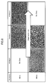
- FIG. 8 illustrates a change of characteristics of the TiN film in high-temperature film deposition.
- SEM Sccanning Electron Microscope
- the sizes of particle sizes of the TiN film are clearly greater in the TIN film at the temperature of 550° C.
- the sizes of particle sizes of the TiN film are greater in the TiN film at the temperature of 610° C.
- the particle sizes of the TiN film become greater in the film deposition process under the higher temperature.
- FIG. 9 illustrates a relationship between a wafer temperature in a process of depositing a film and a film density.
- a result of measuring a relationship between the wafer temperature (° C.) and the film density (g/cm 3 ) by X-ray Reflectivity (XRR) is illustrated.
- FIG. 9 illustrates that the TiN film has a property that the film density increases more as the wafer temperature becomes higher.
- FIG. 10 illustrates a relationship between a wafer temperature in a process of depositing a film and a chloride concentration.
- a result of measuring the relationship between the wafer temperature (° C.) in the process of depositing the film and the chloride concentration (atom %) using a Secondary Ion-Microscope Mass Spectrometer (SIMS) is illustrated.
- FIG. 10 illustrates that the chloride concentration becomes smaller as the wafer temperature is higher in the TiN film.
- the purity of the TiN film is enhanced more so as to obtain a film having a higher purity (that is substantially equal to a higher density) as the wafer temperature is increased because if the purity of the TiN film is high Cl in a raw gas, which contains TiCl 4 and NH 3 for depositing the TiN film, is supposed not to remain much in the TiN film.
- FIGS. 11A and 11B illustrate the mechanism of preventing metallic contamination using the film, whose particle size is great and which is obtained in the film deposition process under the high temperature condition.
- FIG. 11A illustrates an example of a cross-sectional view of the film whose particle size is great.
- FIG. 11B illustrates an example of a cross-sectional view of the film whose particle size is small.
- a molecular particle G 1 existing inside a film F 1 is illustrated. Because the particle size of the molecular particle G 1 is great, a diffusion route R 1 for a metal is choked by the molecular particle G 1 . Therefore, the diffusion route R 1 is extremely narrow.
- FIG. 11B illustrates a molecular particle G 2 existing inside a film F 2 . Because the particle size of the molecular particle G 2 is small, a diffusion route R 2 is widened so that a contaminating metal Mc passes through the diffusion route R 2 .
- a coating film for preventing the contaminating metal Mc from passing through can be provided on the inner surface of the chamber 1 , the surface of the turntable 2 , and surfaces of metallic components inside the chamber 1 by depositing a film whose particle size is great in the coating process so that a film is formed on the inner surface of the chamber 1 , the surface of the turntable 2 , and surfaces of metallic components inside the chamber 1 . Under the state, the wafer W is introduced and the film is formed on the wafer W.
- the temperature of the circular concave portion 24 is set to be higher than the wafer temperature in the processing step or at least the same as the wafer temperature in the processing step, and the coating film having the particle size with which the contaminating metal Mc from being diffused during the film deposition process. With this coating film, the metallic contamination can be prevented.
- the coating film capable of preventing the metallic contamination is deposited before the film deposition process, and thereafter the film deposition process is performed. With this, it is possible to deposit the film with less metallic contamination.
- the temperature of the circular concave portion 24 which is positioned close to the wafer W, is set as the standard instead of the temperature of the wafer W.
- a temperature sensor can be positioned at any place as long as the preset temperature in the coating step and the preset temperature in the processing step can be converted based on the wafer W.
- FIG. 12 illustrates a result of performing the method of depositing the film of the first embodiment.
- the film deposition apparatus of the above embodiment is used.
- the preset temperature in the coating step and the preset temperature in the processing step are variously changed to deposit the TiN film.
- the amount of contamination by copper in the TiN film on the front surface side of the wafer is measured for variously changed preset temperatures.
- the abscissa axis represents the preset temperature (° C.) in the coating step, and the ordinate axis represents the amount of contamination by copper (atoms/cm 2 ).
- the parameter of the film deposition temperature is 420° C., 550° C., and 610° C.
- the parameter of the preset temperature in the processing step is 550° C., 600° C., and 610° C.
- the preset temperature of the coating step is 420° C.
- the amount of contamination by copper was not reduced much under all the preset temperature in the processing step of 550° C., 600° C., and 610° C.
- the preset temperatures in the processing step of 550° C. is relatively close to the preset temperatures in the coating step of 420° C.
- the preset temperatures in the processing step is 600° C. and 610° C., the amount of contamination by copper became great.
- the preset temperature in the coating step is 550° C. and the preset temperature in the processing step is 550° C., which is equal to the preset temperature in the coating step, the amount of contamination by copper was substantially reduced.
- the preset temperature in the coating step is 600° C. and 610° C., which are higher than the preset temperature in the coating step, the amount of contamination by copper increased. Therefore, an excellent inhibiting effect was not obtained.
- the preset temperature in the coating step is 610° C. and the preset temperature in the processing step is equal to or less than the preset temperature in the coating step. Therefore, in this case, copper contamination was not detected at all, and the amount of contamination by copper was zero.
- the preset temperature in the processing step is made equal to or less than the preset temperature in the coating step. With this, the amount of contamination by copper can be reduced.
- the reason why the amount of contamination by copper is selectively measured among various contaminating metals is that copper tends to diffuse and the diffusion of copper greatly affects inside an insulating film such as a TiN film or the like.
- the amount of contamination by copper is one of important features for a person who performs deposition of a film.
- FIG. 13 illustrates a result of performing the method of depositing the film of a second embodiment.
- the film deposition apparatus of the above embodiment is used.
- the preset temperature in the coating step and the preset temperature in the processing step are variously changed to deposit the TiN film.
- the amount of contamination by a metal other than copper in the TiN film on the front surface side of the wafer is measured for variously changed preset temperatures.
- the parameter of the preset temperature in the coating step is 420° C. and 610° C.
- the parameter of the preset temperature in the processing step is 550° C. (on the left side of FIG. 13 ) and 610° C. (on the right side of FIG. 13 ).
- the abscissa axis represents the preset temperature (° C.) in the coating step and the processing step
- the ordinate axis represents the amount of contamination by metal (atoms/cm 2 ).
- the amount of contamination by metal of Cr and Ni was not detected.
- the amount of contamination by metal of other elements i.e., Li, Na, Al, Fe, Cu, and Zn was conspicuously detected.
- the preset temperature in the processing step is 550° C. and the preset temperature in the coating step is 610° C.
- the amount of contamination by a metal other than Cu was not detected. Therefore, in a case where the preset temperature in the coating step is 610° C. and the preset temperature in the processing step is 550° C., which is lower than the preset temperature of the coating step, the amount of contamination by metal can be reduced.
- the amount of contamination by metal of Cr and Ni was not detected.
- the amount of contamination by metal of other elements i.e., Li, Na, Al, Fe, Cu, and Zn was conspicuously detected.
- the preset temperature in the processing step is 610° C. and the preset temperature in the coating step is 610° C.
- the amount of contamination by a metal other than Na and Al was not detected. Therefore, in a case where the preset temperature in the coating step is 610° C. and the preset temperature in the processing step is 610° C., which is equal to the preset temperature of the coating step, the amount of contamination by metal can be reduced.
- the method of depositing the film of the embodiment can cause the amount of contamination by metal of various metals including copper, which are contained in a TiN film, to be reduced.
- the method of depositing the film of the present invention is applied to the deposition of the TiN film
- the content of forming the film on the surface of the wafer W by depositing the film whose particle size is large at the preset temperature in the coating step and depositing the film on the surface of the wafer W at the temperature equal to or less than the preset temperature in the coating step can be applied to a process of forming various films. Therefore, the method of depositing the film of the embodiment, the first embodiment, and the second embodiment can be applied to deposition of another film.
Landscapes
- Chemical & Material Sciences (AREA)
- General Chemical & Material Sciences (AREA)
- Chemical Kinetics & Catalysis (AREA)
- Engineering & Computer Science (AREA)
- Materials Engineering (AREA)
- Mechanical Engineering (AREA)
- Metallurgy (AREA)
- Organic Chemistry (AREA)
- Inorganic Chemistry (AREA)
- Chemical Vapour Deposition (AREA)
- Electrodes Of Semiconductors (AREA)
Abstract
Description
- 1: chamber;
- 2: turntable;
- 4: convex portion;
- 11: ceiling plate;
- 12: chamber body;
- 15: transfer opening;
- 24: circular concave portion (wafer mounting portion);
- 31, 32: reaction gas nozzle;
- 41, 42: separation gas nozzle;
- D: separating area;
- P1: first process area;
- P2: second process area;
- H: separation space;
- W: wafer.
Claims (9)
Applications Claiming Priority (2)
| Application Number | Priority Date | Filing Date | Title |
|---|---|---|---|
| JP2012283175A JP6071537B2 (en) | 2012-12-26 | 2012-12-26 | Deposition method |
| JP2012-283175 | 2012-12-26 |
Publications (2)
| Publication Number | Publication Date |
|---|---|
| US20140179104A1 US20140179104A1 (en) | 2014-06-26 |
| US8921237B2 true US8921237B2 (en) | 2014-12-30 |
Family
ID=50975106
Family Applications (1)
| Application Number | Title | Priority Date | Filing Date |
|---|---|---|---|
| US14/134,065 Active US8921237B2 (en) | 2012-12-26 | 2013-12-19 | Method of depositing a film |
Country Status (3)
| Country | Link |
|---|---|
| US (1) | US8921237B2 (en) |
| JP (1) | JP6071537B2 (en) |
| KR (1) | KR101649783B1 (en) |
Families Citing this family (7)
| Publication number | Priority date | Publication date | Assignee | Title |
|---|---|---|---|---|
| JP6115244B2 (en) * | 2013-03-28 | 2017-04-19 | 東京エレクトロン株式会社 | Deposition equipment |
| KR102264257B1 (en) | 2014-12-30 | 2021-06-14 | 삼성전자주식회사 | Method of forming a layer band method of manufacturing a semiconductor device using the same |
| US9828672B2 (en) | 2015-03-26 | 2017-11-28 | Lam Research Corporation | Minimizing radical recombination using ALD silicon oxide surface coating with intermittent restoration plasma |
| JP6863107B2 (en) * | 2017-06-13 | 2021-04-21 | 東京エレクトロン株式会社 | Film forming equipment, cleaning method of film forming equipment and storage medium |
| JP2021506126A (en) | 2017-12-07 | 2021-02-18 | ラム リサーチ コーポレーションLam Research Corporation | Oxidation resistant protective layer in chamber adjustment |
| US10760158B2 (en) | 2017-12-15 | 2020-09-01 | Lam Research Corporation | Ex situ coating of chamber components for semiconductor processing |
| CN113196451A (en) * | 2018-10-19 | 2021-07-30 | 朗姆研究公司 | In-situ protective coating for chamber components for semiconductor processing |
Citations (6)
| Publication number | Priority date | Publication date | Assignee | Title |
|---|---|---|---|---|
| US6391800B1 (en) * | 1999-11-12 | 2002-05-21 | Motorola, Inc. | Method for patterning a substrate with photoresist |
| US6613700B2 (en) * | 2000-12-14 | 2003-09-02 | Texas Instruments Incorporated | Method for spin coating high viscosity materials on silicon wafers |
| US7018679B2 (en) * | 2001-03-29 | 2006-03-28 | Dürr Systems, Inc. | Coating installation with an atomizer change station |
| JP4583764B2 (en) | 2004-01-14 | 2010-11-17 | ルネサスエレクトロニクス株式会社 | Semiconductor device and manufacturing method thereof |
| JP4661990B2 (en) | 2008-06-27 | 2011-03-30 | 東京エレクトロン株式会社 | Film forming apparatus, film forming method, substrate processing apparatus, and storage medium |
| US8496991B2 (en) * | 2006-09-14 | 2013-07-30 | Tokyo Electron Limited | Coating treatment method |
Family Cites Families (4)
| Publication number | Priority date | Publication date | Assignee | Title |
|---|---|---|---|---|
| JP4325301B2 (en) * | 2003-01-31 | 2009-09-02 | 東京エレクトロン株式会社 | Mounting table, processing apparatus, and processing method |
| KR101173645B1 (en) * | 2007-12-31 | 2012-08-20 | (주)에이디에스 | Gas injection unit and apparatus for depositing thin film having the same |
| JP5346904B2 (en) * | 2009-11-27 | 2013-11-20 | 東京エレクトロン株式会社 | Vertical film forming apparatus and method of using the same |
| JP5482196B2 (en) * | 2009-12-25 | 2014-04-23 | 東京エレクトロン株式会社 | Film forming apparatus, film forming method, and storage medium |
-
2012
- 2012-12-26 JP JP2012283175A patent/JP6071537B2/en active Active
-
2013
- 2013-12-19 US US14/134,065 patent/US8921237B2/en active Active
- 2013-12-20 KR KR1020130159966A patent/KR101649783B1/en active Active
Patent Citations (6)
| Publication number | Priority date | Publication date | Assignee | Title |
|---|---|---|---|---|
| US6391800B1 (en) * | 1999-11-12 | 2002-05-21 | Motorola, Inc. | Method for patterning a substrate with photoresist |
| US6613700B2 (en) * | 2000-12-14 | 2003-09-02 | Texas Instruments Incorporated | Method for spin coating high viscosity materials on silicon wafers |
| US7018679B2 (en) * | 2001-03-29 | 2006-03-28 | Dürr Systems, Inc. | Coating installation with an atomizer change station |
| JP4583764B2 (en) | 2004-01-14 | 2010-11-17 | ルネサスエレクトロニクス株式会社 | Semiconductor device and manufacturing method thereof |
| US8496991B2 (en) * | 2006-09-14 | 2013-07-30 | Tokyo Electron Limited | Coating treatment method |
| JP4661990B2 (en) | 2008-06-27 | 2011-03-30 | 東京エレクトロン株式会社 | Film forming apparatus, film forming method, substrate processing apparatus, and storage medium |
Also Published As
| Publication number | Publication date |
|---|---|
| JP6071537B2 (en) | 2017-02-01 |
| US20140179104A1 (en) | 2014-06-26 |
| KR101649783B1 (en) | 2016-08-19 |
| KR20140083884A (en) | 2014-07-04 |
| JP2014125653A (en) | 2014-07-07 |
Similar Documents
| Publication | Publication Date | Title |
|---|---|---|
| US20140179104A1 (en) | Method of depositing a film | |
| US10590534B2 (en) | Film deposition method and film deposition apparatus | |
| KR101691255B1 (en) | Film deposition apparatus | |
| KR102377033B1 (en) | Apparatus and methods for isolating a reaction chamber from a loading chamber resulting in reduced contamination | |
| TWI523970B (en) | Film forming device (1) | |
| US9136133B2 (en) | Method of depositing film | |
| US9153433B2 (en) | Method of depositing a film and film deposition apparatus | |
| US10604839B2 (en) | Substrate processing apparatus, method of manufacturing semiconductor device, and method of processing substrate | |
| KR101588083B1 (en) | Film forming method | |
| KR101210456B1 (en) | Method of manufacturing semiconductor device, method of processing substrate and substrate processing apparatus | |
| KR101658277B1 (en) | Film deposition apparatus | |
| JP2010126797A (en) | Film deposition system, semiconductor fabrication apparatus, susceptor for use in the same, program and computer readable storage medium | |
| KR101734779B1 (en) | Method for depositing a film | |
| KR20170007132A (en) | Substrate processing apparatus | |
| JP2010263245A (en) | Film forming apparatus, film forming method, substrate processing apparatus, and storage medium | |
| US8895456B2 (en) | Method of depositing a film | |
| US20200040456A1 (en) | Film deposition apparatus and film deposition method | |
| US9293321B2 (en) | Method of manufacturing a silicon oxide film | |
| US10458016B2 (en) | Method for forming a protective film | |
| US12618148B2 (en) | Deposition method and deposition apparatus | |
| US11562905B2 (en) | Method of manufacturing semiconductor device, substrate processing apparatus, and recording medium | |
| JP2016065287A (en) | Semiconductor device manufacturing method, substrate processing apparatus, and program | |
| JP6096955B2 (en) | Deposition method |
Legal Events
| Date | Code | Title | Description |
|---|---|---|---|
| AS | Assignment |
Owner name: TOKYO ELECTRON LIMITED, JAPAN Free format text: ASSIGNMENT OF ASSIGNORS INTEREST;ASSIGNORS:OSHIMO, KENTARO;KOAKUTSU, MASATO;SASAKI, HIROKO;AND OTHERS;REEL/FRAME:031994/0650 Effective date: 20131223 |
|
| FEPP | Fee payment procedure |
Free format text: PAYOR NUMBER ASSIGNED (ORIGINAL EVENT CODE: ASPN); ENTITY STATUS OF PATENT OWNER: LARGE ENTITY |
|
| STCF | Information on status: patent grant |
Free format text: PATENTED CASE |
|
| MAFP | Maintenance fee payment |
Free format text: PAYMENT OF MAINTENANCE FEE, 4TH YEAR, LARGE ENTITY (ORIGINAL EVENT CODE: M1551) Year of fee payment: 4 |
|
| MAFP | Maintenance fee payment |
Free format text: PAYMENT OF MAINTENANCE FEE, 8TH YEAR, LARGE ENTITY (ORIGINAL EVENT CODE: M1552); ENTITY STATUS OF PATENT OWNER: LARGE ENTITY Year of fee payment: 8 |
|
| MAFP | Maintenance fee payment |
Free format text: PAYMENT OF MAINTENANCE FEE, 12TH YEAR, LARGE ENTITY (ORIGINAL EVENT CODE: M1553); ENTITY STATUS OF PATENT OWNER: LARGE ENTITY Year of fee payment: 12 |