US8916468B2 - Semiconductor device fabrication method - Google Patents
Semiconductor device fabrication method Download PDFInfo
- Publication number
- US8916468B2 US8916468B2 US13/911,746 US201313911746A US8916468B2 US 8916468 B2 US8916468 B2 US 8916468B2 US 201313911746 A US201313911746 A US 201313911746A US 8916468 B2 US8916468 B2 US 8916468B2
- Authority
- US
- United States
- Prior art keywords
- insulating film
- forming
- conductive
- film
- conductive via
- Prior art date
- Legal status (The legal status is an assumption and is not a legal conclusion. Google has not performed a legal analysis and makes no representation as to the accuracy of the status listed.)
- Active
Links
Images


Classifications
-
- H01L21/76898—
-
- H—ELECTRICITY
- H10—SEMICONDUCTOR DEVICES; ELECTRIC SOLID-STATE DEVICES NOT OTHERWISE PROVIDED FOR
- H10W—GENERIC PACKAGES, INTERCONNECTIONS, CONNECTORS OR OTHER CONSTRUCTIONAL DETAILS OF DEVICES COVERED BY CLASS H10
- H10W20/00—Interconnections in chips, wafers or substrates
- H10W20/01—Manufacture or treatment
- H10W20/021—Manufacture or treatment of interconnections within wafers or substrates
- H10W20/023—Manufacture or treatment of interconnections within wafers or substrates the interconnections being through-semiconductor vias
-
- H01L21/76802—
-
- H01L21/76807—
-
- H01L21/76816—
-
- H01L21/76846—
-
- H01L21/76849—
-
- H01L21/76877—
-
- H01L23/481—
-
- H01L23/485—
-
- H01L23/522—
-
- H01L25/0657—
-
- H—ELECTRICITY
- H10—SEMICONDUCTOR DEVICES; ELECTRIC SOLID-STATE DEVICES NOT OTHERWISE PROVIDED FOR
- H10W—GENERIC PACKAGES, INTERCONNECTIONS, CONNECTORS OR OTHER CONSTRUCTIONAL DETAILS OF DEVICES COVERED BY CLASS H10
- H10W20/00—Interconnections in chips, wafers or substrates
- H10W20/01—Manufacture or treatment
- H10W20/021—Manufacture or treatment of interconnections within wafers or substrates
- H10W20/023—Manufacture or treatment of interconnections within wafers or substrates the interconnections being through-semiconductor vias
- H10W20/0245—Manufacture or treatment of interconnections within wafers or substrates the interconnections being through-semiconductor vias comprising use of blind vias during the manufacture
-
- H—ELECTRICITY
- H10—SEMICONDUCTOR DEVICES; ELECTRIC SOLID-STATE DEVICES NOT OTHERWISE PROVIDED FOR
- H10W—GENERIC PACKAGES, INTERCONNECTIONS, CONNECTORS OR OTHER CONSTRUCTIONAL DETAILS OF DEVICES COVERED BY CLASS H10
- H10W20/00—Interconnections in chips, wafers or substrates
- H10W20/01—Manufacture or treatment
- H10W20/021—Manufacture or treatment of interconnections within wafers or substrates
- H10W20/023—Manufacture or treatment of interconnections within wafers or substrates the interconnections being through-semiconductor vias
- H10W20/0261—Manufacture or treatment of interconnections within wafers or substrates the interconnections being through-semiconductor vias characterised by the filling method or the material of the conductive fill
-
- H—ELECTRICITY
- H10—SEMICONDUCTOR DEVICES; ELECTRIC SOLID-STATE DEVICES NOT OTHERWISE PROVIDED FOR
- H10W—GENERIC PACKAGES, INTERCONNECTIONS, CONNECTORS OR OTHER CONSTRUCTIONAL DETAILS OF DEVICES COVERED BY CLASS H10
- H10W20/00—Interconnections in chips, wafers or substrates
- H10W20/01—Manufacture or treatment
- H10W20/031—Manufacture or treatment of conductive parts of the interconnections
- H10W20/032—Manufacture or treatment of conductive parts of the interconnections of conductive barrier, adhesion or liner layers
- H10W20/033—Manufacture or treatment of conductive parts of the interconnections of conductive barrier, adhesion or liner layers in openings in dielectrics
- H10W20/035—Manufacture or treatment of conductive parts of the interconnections of conductive barrier, adhesion or liner layers in openings in dielectrics combinations of barrier, adhesion or liner layers, e.g. multi-layered barrier layers
-
- H—ELECTRICITY
- H10—SEMICONDUCTOR DEVICES; ELECTRIC SOLID-STATE DEVICES NOT OTHERWISE PROVIDED FOR
- H10W—GENERIC PACKAGES, INTERCONNECTIONS, CONNECTORS OR OTHER CONSTRUCTIONAL DETAILS OF DEVICES COVERED BY CLASS H10
- H10W20/00—Interconnections in chips, wafers or substrates
- H10W20/01—Manufacture or treatment
- H10W20/031—Manufacture or treatment of conductive parts of the interconnections
- H10W20/056—Manufacture or treatment of conductive parts of the interconnections by filling conductive material into holes, grooves or trenches
-
- H—ELECTRICITY
- H10—SEMICONDUCTOR DEVICES; ELECTRIC SOLID-STATE DEVICES NOT OTHERWISE PROVIDED FOR
- H10W—GENERIC PACKAGES, INTERCONNECTIONS, CONNECTORS OR OTHER CONSTRUCTIONAL DETAILS OF DEVICES COVERED BY CLASS H10
- H10W20/00—Interconnections in chips, wafers or substrates
- H10W20/01—Manufacture or treatment
- H10W20/071—Manufacture or treatment of dielectric parts thereof
- H10W20/081—Manufacture or treatment of dielectric parts thereof by forming openings in the dielectric parts
- H10W20/084—Manufacture or treatment of dielectric parts thereof by forming openings in the dielectric parts for dual-damascene structures
-
- H—ELECTRICITY
- H10—SEMICONDUCTOR DEVICES; ELECTRIC SOLID-STATE DEVICES NOT OTHERWISE PROVIDED FOR
- H10W—GENERIC PACKAGES, INTERCONNECTIONS, CONNECTORS OR OTHER CONSTRUCTIONAL DETAILS OF DEVICES COVERED BY CLASS H10
- H10W20/00—Interconnections in chips, wafers or substrates
- H10W20/01—Manufacture or treatment
- H10W20/071—Manufacture or treatment of dielectric parts thereof
- H10W20/081—Manufacture or treatment of dielectric parts thereof by forming openings in the dielectric parts
- H10W20/089—Manufacture or treatment of dielectric parts thereof by forming openings in the dielectric parts using processes for implementing desired shapes or dispositions of the openings, e.g. double patterning
-
- H—ELECTRICITY
- H10—SEMICONDUCTOR DEVICES; ELECTRIC SOLID-STATE DEVICES NOT OTHERWISE PROVIDED FOR
- H10W—GENERIC PACKAGES, INTERCONNECTIONS, CONNECTORS OR OTHER CONSTRUCTIONAL DETAILS OF DEVICES COVERED BY CLASS H10
- H10W20/00—Interconnections in chips, wafers or substrates
- H10W20/20—Interconnections within wafers or substrates, e.g. through-silicon vias [TSV]
- H10W20/211—Through-semiconductor vias, e.g. TSVs
- H10W20/213—Cross-sectional shapes or dispositions
- H10W20/2134—TSVs extending from the semiconductor wafer into back-end-of-line layers
-
- H—ELECTRICITY
- H10—SEMICONDUCTOR DEVICES; ELECTRIC SOLID-STATE DEVICES NOT OTHERWISE PROVIDED FOR
- H10W—GENERIC PACKAGES, INTERCONNECTIONS, CONNECTORS OR OTHER CONSTRUCTIONAL DETAILS OF DEVICES COVERED BY CLASS H10
- H10W20/00—Interconnections in chips, wafers or substrates
- H10W20/40—Interconnections external to wafers or substrates, e.g. back-end-of-line [BEOL] metallisations or vias connecting to gate electrodes
-
- H—ELECTRICITY
- H10—SEMICONDUCTOR DEVICES; ELECTRIC SOLID-STATE DEVICES NOT OTHERWISE PROVIDED FOR
- H10W—GENERIC PACKAGES, INTERCONNECTIONS, CONNECTORS OR OTHER CONSTRUCTIONAL DETAILS OF DEVICES COVERED BY CLASS H10
- H10W90/00—Package configurations
-
- H01L2224/0382—
-
- H01L2224/0401—
-
- H01L2224/0557—
-
- H01L2224/05572—
-
- H01L2224/06181—
-
- H01L2224/11009—
-
- H01L2224/16145—
-
- H01L2225/06513—
-
- H01L2225/06541—
-
- H01L2225/06544—
-
- H01L2225/06565—
-
- H—ELECTRICITY
- H10—SEMICONDUCTOR DEVICES; ELECTRIC SOLID-STATE DEVICES NOT OTHERWISE PROVIDED FOR
- H10W—GENERIC PACKAGES, INTERCONNECTIONS, CONNECTORS OR OTHER CONSTRUCTIONAL DETAILS OF DEVICES COVERED BY CLASS H10
- H10W20/00—Interconnections in chips, wafers or substrates
- H10W20/01—Manufacture or treatment
- H10W20/031—Manufacture or treatment of conductive parts of the interconnections
- H10W20/032—Manufacture or treatment of conductive parts of the interconnections of conductive barrier, adhesion or liner layers
- H10W20/033—Manufacture or treatment of conductive parts of the interconnections of conductive barrier, adhesion or liner layers in openings in dielectrics
- H10W20/037—Manufacture or treatment of conductive parts of the interconnections of conductive barrier, adhesion or liner layers in openings in dielectrics the barrier, adhesion or liner layers being on top of a main fill metal
-
- H—ELECTRICITY
- H10—SEMICONDUCTOR DEVICES; ELECTRIC SOLID-STATE DEVICES NOT OTHERWISE PROVIDED FOR
- H10W—GENERIC PACKAGES, INTERCONNECTIONS, CONNECTORS OR OTHER CONSTRUCTIONAL DETAILS OF DEVICES COVERED BY CLASS H10
- H10W72/00—Interconnections or connectors in packages
- H10W72/01—Manufacture or treatment
- H10W72/012—Manufacture or treatment of bump connectors, dummy bumps or thermal bumps
- H10W72/01204—Manufacture or treatment of bump connectors, dummy bumps or thermal bumps using temporary auxiliary members, e.g. using sacrificial coatings or handle substrates
-
- H—ELECTRICITY
- H10—SEMICONDUCTOR DEVICES; ELECTRIC SOLID-STATE DEVICES NOT OTHERWISE PROVIDED FOR
- H10W—GENERIC PACKAGES, INTERCONNECTIONS, CONNECTORS OR OTHER CONSTRUCTIONAL DETAILS OF DEVICES COVERED BY CLASS H10
- H10W72/00—Interconnections or connectors in packages
- H10W72/01—Manufacture or treatment
- H10W72/019—Manufacture or treatment of bond pads
-
- H—ELECTRICITY
- H10—SEMICONDUCTOR DEVICES; ELECTRIC SOLID-STATE DEVICES NOT OTHERWISE PROVIDED FOR
- H10W—GENERIC PACKAGES, INTERCONNECTIONS, CONNECTORS OR OTHER CONSTRUCTIONAL DETAILS OF DEVICES COVERED BY CLASS H10
- H10W72/00—Interconnections or connectors in packages
- H10W72/20—Bump connectors, e.g. solder bumps or copper pillars; Dummy bumps; Thermal bumps
- H10W72/29—Bond pads specially adapted therefor
-
- H—ELECTRICITY
- H10—SEMICONDUCTOR DEVICES; ELECTRIC SOLID-STATE DEVICES NOT OTHERWISE PROVIDED FOR
- H10W—GENERIC PACKAGES, INTERCONNECTIONS, CONNECTORS OR OTHER CONSTRUCTIONAL DETAILS OF DEVICES COVERED BY CLASS H10
- H10W72/00—Interconnections or connectors in packages
- H10W72/90—Bond pads, in general
- H10W72/921—Structures or relative sizes of bond pads
- H10W72/923—Bond pads having multiple stacked layers
-
- H—ELECTRICITY
- H10—SEMICONDUCTOR DEVICES; ELECTRIC SOLID-STATE DEVICES NOT OTHERWISE PROVIDED FOR
- H10W—GENERIC PACKAGES, INTERCONNECTIONS, CONNECTORS OR OTHER CONSTRUCTIONAL DETAILS OF DEVICES COVERED BY CLASS H10
- H10W72/00—Interconnections or connectors in packages
- H10W72/90—Bond pads, in general
- H10W72/941—Dispositions of bond pads
- H10W72/9415—Dispositions of bond pads relative to the surface, e.g. recessed, protruding
-
- H—ELECTRICITY
- H10—SEMICONDUCTOR DEVICES; ELECTRIC SOLID-STATE DEVICES NOT OTHERWISE PROVIDED FOR
- H10W—GENERIC PACKAGES, INTERCONNECTIONS, CONNECTORS OR OTHER CONSTRUCTIONAL DETAILS OF DEVICES COVERED BY CLASS H10
- H10W72/00—Interconnections or connectors in packages
- H10W72/90—Bond pads, in general
- H10W72/941—Dispositions of bond pads
- H10W72/942—Dispositions of bond pads relative to underlying supporting features, e.g. bond pads, RDLs or vias
-
- H—ELECTRICITY
- H10—SEMICONDUCTOR DEVICES; ELECTRIC SOLID-STATE DEVICES NOT OTHERWISE PROVIDED FOR
- H10W—GENERIC PACKAGES, INTERCONNECTIONS, CONNECTORS OR OTHER CONSTRUCTIONAL DETAILS OF DEVICES COVERED BY CLASS H10
- H10W72/00—Interconnections or connectors in packages
- H10W72/90—Bond pads, in general
- H10W72/941—Dispositions of bond pads
- H10W72/944—Dispositions of multiple bond pads
-
- H—ELECTRICITY
- H10—SEMICONDUCTOR DEVICES; ELECTRIC SOLID-STATE DEVICES NOT OTHERWISE PROVIDED FOR
- H10W—GENERIC PACKAGES, INTERCONNECTIONS, CONNECTORS OR OTHER CONSTRUCTIONAL DETAILS OF DEVICES COVERED BY CLASS H10
- H10W90/00—Package configurations
- H10W90/20—Configurations of stacked chips
- H10W90/26—Configurations of stacked chips the stacked chips being of the same size without any chips being laterally offset, e.g. chip stacks having a rectangular shape
-
- H—ELECTRICITY
- H10—SEMICONDUCTOR DEVICES; ELECTRIC SOLID-STATE DEVICES NOT OTHERWISE PROVIDED FOR
- H10W—GENERIC PACKAGES, INTERCONNECTIONS, CONNECTORS OR OTHER CONSTRUCTIONAL DETAILS OF DEVICES COVERED BY CLASS H10
- H10W90/00—Package configurations
- H10W90/20—Configurations of stacked chips
- H10W90/297—Configurations of stacked chips characterised by the through-semiconductor vias [TSVs] in the stacked chips
-
- H—ELECTRICITY
- H10—SEMICONDUCTOR DEVICES; ELECTRIC SOLID-STATE DEVICES NOT OTHERWISE PROVIDED FOR
- H10W—GENERIC PACKAGES, INTERCONNECTIONS, CONNECTORS OR OTHER CONSTRUCTIONAL DETAILS OF DEVICES COVERED BY CLASS H10
- H10W90/00—Package configurations
- H10W90/701—Package configurations characterised by the relative positions of pads or connectors relative to package parts
- H10W90/721—Package configurations characterised by the relative positions of pads or connectors relative to package parts of bump connectors
- H10W90/722—Package configurations characterised by the relative positions of pads or connectors relative to package parts of bump connectors between stacked chips
Definitions
- a technique for forming a conductive via in a semiconductor substrate used in a semiconductor device and electrically connecting the upper and under sides of the semiconductor device by the use of the conductive via is known.
- such a semiconductor device is used in plurality for fabricating an apparatus having a stacked structure in which they are stacked and in which they are electrically connected to one another.
- the following method is known as a method for forming a conductive via in a semiconductor substrate.
- a wiring layer is formed on an upper side of a semiconductor substrate. After that, a via hole is made in the semiconductor substrate and the via hole is filled in with a conductive material.
- the conductive vias are formed in the semiconductor substrate in addition to elements, such as transistors.
- a fabrication process may become complex.
- the conductive vias are formed in the semiconductor substrate, for example, after the formation of a wiring layer, then it may be impossible from the viewpoint of a fabrication process to form the conductive vias with accuracy.
- a semiconductor device fabrication method including forming a transistor with a source and a drain on a semiconductor substrate, forming a first insulating film over the transistor, forming, in the first insulating film, a first conductive via which reaches the source or the drain, forming an opening which pierces the first insulating film and which reaches an inside of the semiconductor substrate, forming a second insulating film on a sidewall of the opening, forming a conductive layer over the first insulating film and in the opening, removing the conductive layer over the first insulating film by polishing to form a second conductive via in the opening, forming a third insulating film over the first insulating film and the second conductive via, and forming, in the third insulating film, a third conductive via which reaches the first conductive via and a fourth conductive via which reaches the second conductive via.
- FIGS. 1A , 1 B, 1 C, 1 D, and 1 E illustrate an example of a semiconductor device fabrication method according to a first embodiment
- FIG. 2 illustrates an example of a semiconductor device having a stacked structure, according to the first embodiment
- FIGS. 3A , 3 B, and 3 C are views for describing an example of a plug formation step in the first embodiment
- FIGS. 4A , 4 B, and 4 C are views for describing an example of a TSV via hole formation step in the first embodiment
- FIGS. 5A and 5B are views for describing an example of a TSV via hole filling step in the first embodiment
- FIGS. 6A , 6 B, and 6 C are views for describing an example of a polishing and cap film formation step in the first embodiment
- FIGS. 7A and 7B are views for describing an example of a wiring layer formation step in the first embodiment
- FIGS. 8A , 8 B, 8 C, and 8 D illustrate another example of a semiconductor device fabrication method
- FIGS. 9A , 9 B, 9 C, and 9 D illustrate still another example of a semiconductor device fabrication method
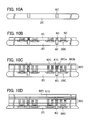
- FIGS. 10A , 10 B, 100 , and 10 D illustrate still another example of a semiconductor device fabrication method
- FIGS. 11A , 11 B, and 11 C are views for describing an example of a TSV via hole formation step in a second embodiment
- FIGS. 12A , 12 B, and 12 C are views for describing an example of an insulating film formation and mask layer removal step in the second embodiment
- FIG. 13 illustrates an example of a state after the etching of a second mask layer and an insulating film in the second embodiment
- FIGS. 14A and 14B are views for describing an example of a via hole filling step in the second embodiment
- FIGS. 15A , 15 B, and 15 C are views for describing an example of a polishing and cap film formation step in the second embodiment
- FIG. 16 is a view for describing an example of a via hole filling step in a third embodiment
- FIGS. 17A , 17 B, and 17 C are views for describing an example of a polishing and cap film formation step in the third embodiment
- FIGS. 18A , 18 B, 18 C, 18 D, and 18 E illustrate an example of a semiconductor device fabrication method according to a fourth embodiment
- FIGS. 19A , 19 B, and 19 C are views for describing an example of a wiring groove formation step in the fourth embodiment
- FIGS. 20A , 20 B, and 20 C are views for describing an example of a via hole making step in the fourth embodiment
- FIGS. 21A , 21 B, and 21 C are views for describing an example of an insulating film formation and mask layer removal step in the fourth embodiment
- FIG. 22 is a view for describing an example of a via hole filling step in the fourth embodiment.
- FIGS. 23A , 23 B, and 23 C are views for describing an example of a polishing and cap film formation step in the fourth embodiment
- FIGS. 24A and 24B are views for describing an example of a wiring layer formation step in the fourth embodiment
- FIG. 25 is a view for describing another example of a wiring layer formation step in the fourth embodiment.
- FIG. 26 is a view for describing an example of a semiconductor device.
- FIGS. 1A , 1 B, 1 C, 1 D, and 1 E illustrate an example of a semiconductor device fabrication method according to a first embodiment.
- FIG. 1A a semiconductor substrate 2 , such as a silicon (Si) substrate, is prepared and isolation regions 3 are formed at determined positions in the semiconductor substrate 2 .
- FIG. 1A illustrates the isolation regions 3 formed by an STI (shallow Trench Isolation) method.
- a transistor 20 is then formed in an element region defined by the isolation regions 3 .
- a well region 24 of a determined conduction type is formed in the element region.
- the transistor 20 is formed in this well region 24 .
- FIG. 1A illustrates as the transistor 20 a MOS transistor including a gate electrode formed over the semiconductor substrate 2 with a gate insulating film 21 between and impurity diffusion regions 23 of a determined conduction type formed on both sides of the gate electrode 22 in the semiconductor substrate 2 .
- the impurity diffusion regions 23 on both sides of the gate electrode 22 function as a source and a drain of the transistor 20 .
- an insulating film 4 which covers the transistor 20 is formed.
- Conductive vias (plugs) 5 which pierce the insulating film 4 and which reach the impurity diffusion regions 23 of the transistor 20 and a conductive via 6 which pierces the insulating film 4 and which reaches the inside of the semiconductor substrate 2 are then formed.
- an insulating film (not illustrated) is formed between the semiconductor substrate 2 and the conductive via 6 in order to prevent leakage current from flowing between them.
- a multilayer interconnection 30 including conductive portions 30 a , such as wirings and vias, which are electrically connected to the conductive vias 5 and 6 and an insulating layer 30 b which covers the conductive portions 30 a is formed.
- the number of wiring layers included in the multilayer interconnection 30 is not limited to that illustrated in FIGS. 1A , 1 B, 1 C, 1 D, and 1 E.
- a pad 41 and a cover film 42 are formed over the multilayer interconnection 30 .
- FIG. 10 illustrates the pad 41 electrically connected to the conductive via 6 which reaches the inside of the semiconductor substrate 2 .
- a support board 52 is stuck on a side on which the multilayer interconnection 30 is formed by the use of an adhesive 51 .
- a back of the semiconductor substrate 2 (side opposite to the side on which the support board 52 is stuck) is then ground (back grind) so that the conductive via 6 formed in the semiconductor substrate 2 will get exposed. By doing so, what is called a through silicon via (TSV) is obtained. This via pierces the semiconductor substrate 2 .
- TSV through silicon via
- an insulating film 61 is formed over the back of the semiconductor substrate 2 , an adherent conductive layer 63 and a bump 62 are formed over the conductive via 6 which gets exposed on the back, and the adhesive 51 and the support board 52 on the side on which the multilayer interconnection 30 is formed are removed.
- dicing is performed, for example, at positions indicated by dotted lines in FIG. 1E to cut a wafer into individual semiconductor devices 1 .
- Individual semiconductor devices 1 can be stacked to form a semiconductor device having a stacked structure.
- FIG. 2 illustrates an example of a semiconductor device having a stacked structure, according to the first embodiment.
- FIGS. 3A , 3 B, and 3 C are views for describing an example of a plug formation step in the first embodiment.
- FIG. 3A is a fragmentary schematic sectional view of a plug via hole formation step.
- FIG. 3B is a fragmentary schematic sectional view of a plug material formation step.
- FIG. 3C is a fragmentary schematic sectional view of a plug material polishing step.
- the insulating film 4 which covers the transistor 20 is formed over the semiconductor substrate 2 in which the transistor 20 is formed.
- the insulating film 4 having a two-layer structure of insulating films 4 a and 4 b is formed as an example.
- a silicon nitride (SiN) film for example, is formed as the lower insulating film 4 a .
- a silicon oxide (SiO 2 ) film for example, is formed as the upper insulating film 4 b .
- the insulating film 4 (insulating films 4 a and 4 b ) is formed by, for example, a CVD (Chemical Vapor Deposition) method. In that case, CMP (Chemical Mechanical Polishing) is performed for planarization after the insulating film 4 is deposited by the CVD method.
- the thickness of the insulating film 4 is, for example, 200 to 400 nm.
- via holes (contact holes) 5 a which pierce the insulating film 4 and which reach the impurity diffusion regions 23 (source and the drain) of the transistor 20 are formed.
- the diameter of the via holes 5 a is, for example, 40 to 200 nm.
- the height of the via holes 5 a is equal to the thickness (200 to 400 nm, for example) of the insulating film 4 .
- a conductive layer 5 c such as a tungsten (W) layer, is formed as a plug material in the via holes 5 a and over the insulating film 4 with a barrier metal film (barrier film) 5 b between.
- a barrier metal film (barrier film) 5 b for example, a layer of one of titanium (Ti), tantalum (Ta), titanium nitride (TiN), and tantalum nitride (TaN) or a lamination layer of two or more of them is formed as the barrier metal film 5 b by a sputtering method, the CVD method, or the like.
- the barrier metal film 5 b carries out the function of preventing an element from diffusing from the W layer 5 c .
- the W layer 5 c is formed by, for example, the CVD method.
- the barrier metal film 5 b and the W layer 5 c formed over the insulating film 4 are removed by polishing.
- the barrier metal film 5 b and the W layer 5 c are polished by the CMP until the insulating film 4 gets exposed.
- the conductive vias 5 are formed in the via holes 5 a . That is to say, the W layer 5 c is formed in the via holes 5 a with the barrier metal film 5 b between.
- FIGS. 4A , 4 B, and 4 C are views for describing an example of a TSV via hole formation step in the first embodiment.
- FIG. 4A is a fragmentary schematic sectional view of a mask layer formation step.
- FIG. 4B is fragmentary schematic sectional view of a resist pattern formation step.
- FIG. 4C is a fragmentary schematic sectional view of a TSV via hole formation step.
- a first mask layer 7 and a second mask layer 8 are formed over the conductive vias 5 and the insulating film 4 .
- a SiN film with a thickness of 50 to 100 nm is formed by the CVD method as the first mask layer 7 .
- a SiO 2 film with a thickness of 100 to 200 nm is formed by the CVD method as the second mask layer 8 .
- a resist pattern 9 having an opening 9 a at a position at which a TSV is to be formed is formed over the second mask layer 8 .
- the diameter of the opening 9 a is, for example, 10 to 50 ⁇ m.
- the thickness of the resist pattern 9 is, for example, 2 to 4 ⁇ m.
- etching is performed with it as a mask.
- a TSV via hole (opening) 6 a which pierces the second mask layer 8 , the first mask layer 7 , and the insulating film 4 and which reaches the inside of the semiconductor substrate 2 is formed.
- the second mask layer 8 is etched with the resist pattern 9 as a mask. If the second mask layer 8 is a SiO 2 film, then the second mask layer 8 is etched by the use of, for example, argon (Ar) and hexafluorobutane (C 4 F 6 ).
- the first mask layer 7 is etched. If the first mask layer 7 is a SiN film, then the first mask layer 7 is etched by the use of, for example, Ar, difluoromethane (CH 2 F 2 ), and oxygen (O 2 ).
- the insulating film 4 is etched. If the insulating film 4 includes two layers, that is to say, a SiN film (insulating film 4 a ) and a SiO 2 film (insulating film 4 b ), then the SiO 2 film is etched by the use of, for example, Ar and C 4 F 6 and the SiN film is etched by the use of, for example, Ar, CH 2 F 2 , and O 2 .
- the semiconductor substrate 2 is etched. If the semiconductor substrate 2 is a Si substrate, then the semiconductor substrate 2 is etched by the use of, for example, hexafluorosulfide (SF 6 ) and O 2 .
- SF 6 hexafluorosulfide
- the via hole 6 a which reaches the inside of the semiconductor substrate 2 is made in this way.
- the depth of the via hole 6 a is, for example, 100 to 200 ⁇ m.
- FIGS. 5A and 5B are views for describing an example of a TSV via hole filling step in the first embodiment.
- FIG. 5A is a fragmentary schematic sectional view of an insulating film formation step.
- FIG. 5B is a fragmentary schematic sectional view of a TSV material formation step.
- an insulating film 10 is formed over an inside of the via hole 6 a .
- a silicon carbide (SiC) film, a SiO 2 film, or a SiN film is formed as the insulating film 10 .
- the insulating film 10 can be formed by the CVD method. In that case, as illustrated in FIG. 5A , the insulating film 10 is formed over the inside of the via hole 6 a and the second mask layer 8 .
- the insulating film 10 is formed so that the thickness of the insulating film 10 formed over the inside of the via hole 6 a will be, for example, about 100 nm.
- the insulating film 10 formed over the inside of the via hole 6 a carries out the function of preventing leakage current from flowing to the semiconductor substrate 2 . That is to say, when the via hole 6 a is filled in with a metal material as described later, the insulating film 10 prevents the metal material from diffusing into the semiconductor substrate 2 , prevents the surface of the semiconductor substrate 2 in the via hole 6 a from changing into silicide, and prevents leakage current from flowing to the semiconductor substrate 2 .
- a conductive layer 6 c is formed in the via hole 6 a and over the insulating film 10 as a TSV material with a barrier metal film (barrier film) 6 b between.
- a layer of one of Ti, Ta, TiN, and TaN or a lamination layer of two or more of them is formed as the barrier metal film 6 b by the sputtering method, the CVD method, or the like.
- the thickness of the barrier metal film 6 b is, for example, 30 to 100 nm.
- the barrier metal film 6 b carries out the function of preventing an element from diffusing from the conductive layer 6 c
- a copper (Cu) layer or a layer made mainly of Cu is formed as the conductive layer 6 c by a plating method.
- the conductive layer 6 c is formed by the plating method in the following way.
- a seed layer is formed over the barrier metal film 6 b and the conductive layer 6 c is formed by an electrolytic plating process by the use of the seed layer.
- the via hole 6 a is filled in with the barrier metal film 6 b and the conductive layer 6 c in this way.
- FIGS. 6A , 6 B, and 6 C are views for describing an example of a polishing and cap film formation step in the first embodiment.
- FIG. 6A is a fragmentary schematic sectional view of a TSV material polishing step.
- FIG. 6B is a fragmentary schematic sectional view of a cap film material formation step.
- FIG. 6C is a fragmentary schematic sectional view of a cap film material polishing step.
- the conductive layer 6 c and the barrier metal film 6 b formed over the insulating film 10 are removed by polishing and the insulating film 10 and the second mask layer 8 are removed by polishing.
- the first mask layer 7 gets exposed.
- the first mask layer 7 functions as a stopper.
- the conductive layer 6 c , the barrier metal film 6 b , the insulating film 10 , and the second mask layer 8 can be polished by the CMP.
- the conductive layer 6 c is formed in the via hole 6 a with the barrier metal film 6 b between and the conductive via 6 is formed in the via hole 6 a.
- the conductive layer 6 c , the barrier metal film 6 b , the insulating film 10 , and the second mask layer 8 are polished so that there will be a difference in level between an upper side 6 d of the conductive via 6 after the polishing and an upper side 7 a of the first mask layer 7 (upper end of the via hole 6 a after the polishing).
- a hollow 6 f is made in this way over the conductive via 6 and, as described later, a cap film (metal cap film) made mainly of metal is formed in the hollow 6 f .
- the hollow 6 f is made so that it will have depth by which the upper side 6 d of the conductive via 6 is lower than an under side 7 b of the first mask layer 7 (upper side of the insulating film 4 ).
- the hollow 6 f can be made by making a dishing occur at the time of polishing the conductive layer 6 c , the barrier metal film 6 b , the insulating film 10 , and the second mask layer 8 .
- the diameter (10 to 50 nm in this example) of the conductive via 6 which is to be used as a TSV is larger than that of the conductive vias 5 which are to be used as plugs, so a dishing tends to occur in the conductive layer 6 c at polishing time. Such a dishing occurs and the above hollow 6 f is made. In order to control the depth of the hollow 6 f , polishing conditions are adjusted.
- a dishing can be made to occur, and the hollow 6 f having desired depth can be made.
- a metal layer 11 a (cap film material) for a metal cap film is formed in the hollow 6 f and over the first mask layer 7 as illustrated in FIG. 6B .
- the metal layer 11 a can be formed by the plating method.
- the metal layer 11 a is formed in the hollow 6 f and over the first mask layer 7 by an electroless plating method.
- a seed layer is formed over an inside of the hollow 6 f and the upper side 7 a of the first mask layer 7 and is used for forming the metal layer 11 a by the electrolytic plating process.
- the metal layer 11 a can be formed by a film formation method, such as an ALD (Atomic Layer Deposition) method or the CVD method, other than these plating methods.
- a cobalt tungsten phosphorus (CoWP) layer is formed as the metal layer 11 a .
- a layer which contains zirconium boride (ZrB), W, Ti, Ta, cobalt (Co), ruthenium (Ru), platinum (Pt), ruthenium tungsten (RuW), cobalt tungsten (CoW), or the like can be formed as the metal layer 11 a.
- the metal layer 11 a formed over the upper side 7 a of the first mask layer 7 is removed by polishing and the first mask layer 7 is removed by polishing.
- the metal layer 11 a and the first mask layer 7 can be polished by the CMP.
- the first mask layer 7 functions as a stopper.
- the hollow 6 f is made more deeply than the first mask layer 7 and the metal layer 11 a is formed in the hollow 6 f .
- the metal layer 11 a remains on the surface of the conductive via 6 after the polishing of the metal layer 11 a and the first mask layer 7 .
- the metal layer 11 a which remains on the surface of the conductive via 6 functions as a metal cap film 11 .
- the metal cap film 11 carries out the function of preventing a conductive material, such as Cu, with which the via hole 6 a having great volume is filled in from diffusing outside the via hole 6 a .
- the metal cap film 11 carries out the function of improving adhesion of an insulating film (cap film 33 a described later, for example) formed over the metal cap film 11 .
- the multilayer interconnection 30 including wiring layers is formed.
- FIGS. 7A and 7B are views for describing an example of a wiring layer formation step in the first embodiment.
- FIG. 7A is a fragmentary schematic sectional view of a cap film and interlayer dielectric formation step.
- FIG. 7B is a fragmentary schematic sectional view of a wiring and conductive via formation step.
- an insulating cap film 33 a is formed as illustrated in FIG. 7A .
- an interlayer dielectric 33 b is formed over the cap film 33 a .
- a SiC film with a thickness of 30 to 100 nm is formed as the cap film 33 a by the CVD method.
- a SiO 2 or silicon oxide carbide (SiOC) film with a thickness of 100 to 400 nm is formed as the interlayer dielectric 33 b by the CVD method.
- each wiring 31 a includes a barrier metal film (barrier film) 31 b and a conductive layer 31 c formed with the barrier metal film 31 b between.
- Each wiring 32 a includes a barrier metal film (barrier film) 32 b and a conductive layer 32 c formed with the barrier metal film 32 b between.
- the barrier metal films 31 b and 32 b carry out the function of preventing an element from diffusing from the conductive layers 31 c and 32 c respectively.
- the wirings 31 a are formed so as to pierce the cap film 33 a and the interlayer dielectric 33 b and to reach the conductive vias 5 connected to the impurity diffusion regions 23 (source and the drain) of the transistor 20 . As illustrated in FIG. 7B , a wiring 31 a may not be formed over a conductive via 5 .
- the wirings 32 a are formed so as to pierce the cap film 33 a and the interlayer dielectric 33 b and to reach the metal cap film 11 over the conductive via 6 .
- the wirings 32 a are formed so that they will be electrically connected to the one conductive via 6 .
- wirings 31 a and 32 a can be formed in block by a single damascene process. That is to say, wiring grooves 31 d and 32 d which pierce the cap film 33 a and the interlayer dielectric 33 b are formed first at determined positions by photolithography and etching. A barrier metal film and a conductive layer are then formed in the wiring grooves 31 d and 32 d and over the interlayer dielectric 33 b . The barrier metal film and the conductive layer formed over the interlayer dielectric 33 b are removed by the CMP. As a result, the conductive layer 31 c is formed in the wiring grooves 31 d with the barrier metal film 31 b between and the wirings 31 a are obtained in the wiring grooves 31 d . Furthermore, the conductive layer 32 c is formed in the wiring grooves 32 d with the barrier metal film 32 b between and the wirings 32 a are obtained in the wiring grooves 32 d.
- a first wiring layer in the multilayer interconnection 30 is formed in this way.
- Second and later wiring layers can be formed in the same way as the first wiring layer is formed. That is to say, after the formation of the wirings 31 a and 32 a , a cap film with determined thickness and an interlayer dielectric with determined thickness are formed over the interlayer dielectric 33 b , wirings and vias which pierce the formed cap film and interlayer dielectric are formed at determined positions, and the second wiring layer in the multilayer interconnection 30 is formed.
- a third and later wiring layers in the multilayer interconnection 30 are formed through the same procedure.
- the wirings 31 a and 32 a in the first wiring layer are formed by the single damascene process. However, when each wiring layer in the multilayer interconnection is formed, wirings and vias may be formed by a dual damascene process.
- a determined number of wiring layers are formed through the above procedure and the multilayer interconnection 30 is obtained.
- the pad 41 and the cover film 42 are formed over the multilayer interconnection 30 .
- back grind of the semiconductor substrate 2 is performed so that the conductive via 6 will get exposed, the bump 62 and the like are formed, dicing is performed, and individual semiconductor devices 1 are completed.
- the conductive via 6 formed in the above way gets exposed by the back grind, it is desirable from the viewpoint of the formation of a low-resistance TSV that the conductive layer 6 c of the conductive via 6 made of Cu or made mainly of Cu get exposed on the back of the semiconductor substrate 2 . That is to say, it is desirable to perform back grind to a position indicated by a dotted line for convenience in FIG. 7B .
- the transistor 20 is formed, the conductive vias 5 connected to the transistor and the conductive via 6 which reaches the inside of the semiconductor substrate 2 are formed, and then the multilayer interconnection 30 is formed.
- FIGS. 8A , 8 B, 8 C, and 8 D illustrate another example of a semiconductor device fabrication method.
- a transistor 20 A is formed in a semiconductor substrate 2 A. After an insulating film 4 A which covers the transistor 20 A and conductive vias 5 A connected to the transistor 20 A are formed, a multilayer interconnection 30 A including conductive portions 30 Aa and an insulating layer 30 Ab is formed over the insulating film 4 A.
- a conductive via 6 A which pierces the multilayer interconnection 30 A and the insulating film 4 A and which reaches the inside of the semiconductor substrate 2 A.
- an insulating film (not illustrated) corresponding to the insulating film 10 described in the above first embodiment is formed over an inside of a via hole 6 Aa.
- a rewiring 6 Ab connected to the conductive via 6 A is formed as an uppermost layer by, foe example, a damascene process.
- a pad 41 A and a cover film 42 A are formed over the multilayer interconnection 30 A in which the conductive via 6 A and the like are formed.
- back grind of the semiconductor substrate 2 A is performed by the use of an adhesive 51 A and a support board 52 A so that the conductive via 6 A will get exposed on a back of the semiconductor substrate 2 A.
- the conductive via 6 A is formed in the following way.
- the via hole 6 Aa is formed at the next step illustrated in FIG. 8B .
- the via hole 6 Aa is formed by etching so that it will pierce all wiring layers (insulating layer 30 Ab) included in the multilayer interconnection 30 A and the insulating film 4 A and so that it will reach the inside of the semiconductor substrate 2 A.
- the insulating layer 30 Ab includes films, such as a cap film and an interlayer dielectric, which differ in the quality of material.
- the via hole 6 Aa when the via hole 6 Aa is formed, it is necessary to etch the insulating layer 30 Ab including the films which differ in the quality of material. If the films which differ in the quality of material are etched in order from the top by changing etching conditions, then an etching process becomes complex. Furthermore, if all the films are etched in block, it may be impossible to make the via hole 6 Aa with accuracy. For example, a sidewall of the via hole 6 Aa may become irregular. For example, if the sidewall of the via hole 6 Aa becomes irregular, a barrier metal film is not formed uniformly on the sidewall of the via hole 6 Aa. That is to say, a formed barrier metal film does not cover all of the sidewall of the via hole 6 Aa. Accordingly, leakage current may flow between the conductive via 6 A and the semiconductor substrate 2 A.
- the via hole 6 Aa which pierces the multilayer interconnection 30 A is made and the conductive via 6 A is formed in the via hole 6 Aa. Accordingly, a wiring or a via may not be formed at a position in the multilayer interconnection 30 A at which the conductive via 6 A is to be formed later. Furthermore, a dummy wiring may not be formed at a position in the multilayer interconnection 30 A at which the conductive via 6 A is to be formed later.
- a dummy wiring is often formed in a multilayer interconnection in order to secure the flatness of each layer (in order to avoid a dishing in a conductive portion) in the CMP performed in a multilayer interconnection formation process.
- a conductive via which reaches the inside of a semiconductor substrate is formed after the formation of a multilayer interconnection, then a dummy wiring is arranged at a position other than a position at which the conductive via is to be formed. As a result, for example, it may be impossible to secure the flatness of each wiring layer in the multilayer interconnection.
- a deterioration in the flatness of a first wiring layer leads to a decrease in the accuracy of exposure in photolithography performed at the time of forming a second wiring layer over the first wiring layer. Accordingly, it may be impossible to accurately form a conductive via and a wiring in the second wiring layer.
- a conductive via which reaches the inside of a semiconductor substrate is formed after the formation of a multilayer interconnection in which a dummy wiring is arranged, then a position at which the conductive via can be formed may be influenced by the arrangement of the dummy wiring.
- the conductive via 6 which reaches the inside of the semiconductor substrate 2 is formed before the multilayer interconnection 30 is formed.
- the via hole 6 a in which the conductive via 6 is formed can be formed by etching the insulating film 4 and the semiconductor substrate 2 by the use of the first mask layer 7 and the second mask layer 8 .
- the via hole 6 Aa is made after the multilayer interconnection 30 A is formed. In this case, an etching process becomes complex or the via hole 6 Aa may not be made with accuracy.
- these problems do not arise in the method according to the above first embodiment for fabricating the semiconductor device 1 .
- the conductive via 6 is formed before the multilayer interconnection 30 is formed. Accordingly, even if a dummy wiring is arranged in the multilayer interconnection 30 , the dummy wiring can be arranged more flexibly. This makes it possible to form the multilayer interconnection 30 including wiring layers with good flatness and connection accuracy and to prevent a position at which the conductive via 6 is formed and a position at which a dummy wiring is formed from influencing each other.
- a conductive via which pierces a semiconductor substrate
- TSV conductive via
- a method in which a conductive via is formed by forming a via hole from a semiconductor substrate side may be adopted in addition to the above method which is described in FIGS. 8A , 8 B, 8 C, and 8 D and in which a conductive via is formed by forming a via hole from a multilayer interconnection side.
- FIGS. 9A , 9 B, 9 C, and 9 D illustrate still another example of a semiconductor device fabrication method.
- a transistor 20 B is formed in a semiconductor substrate 2 B.
- a multilayer interconnection 30 B including conductive portions 30 Ba and an insulating layer 30 Bb is formed over the insulating film 4 B.
- a pad 41 B and a cover film 42 B are formed over the multilayer interconnection 30 B.
- back grind of the semiconductor substrate 2 B is performed by the use of an adhesive 51 B and a support board 52 B.
- an insulating protection film 61 B in which an opening 61 Ba is formed at a position at which a conductive via (TSV) is to be formed is formed over a surface (ground surface) of the semiconductor substrate 2 B on which back grind has been performed.
- TSV conductive via
- the opening 61 Ba is formed by photolithography and etching.
- Etching is then performed with the protection film 61 B as a mask.
- a via hole 6 Ba which pierces the semiconductor substrate 2 B and the insulating film 4 B and which reaches the multilayer interconnection 30 B is formed and a conductive via 6 B is formed in the via hole 6 Ba.
- an insulating film (not illustrated) corresponding to the insulating film 10 described in the above first embodiment is formed over an inside of the via hole 6 Ba.
- a wiring 34 B which functions as a stopper at the time of making the via hole 6 Ba and which is to be connected to the conductive via 6 B formed in the via hole 6 Ba is formed in advance in the multilayer interconnection 30 B.
- the wiring 34 B is formed in a first wiring layer of the multilayer interconnection 30 B formed over the insulating film 4 B.
- the protection film 61 B in which the opening 61 Ba is formed is formed over the side of the semiconductor substrate 2 B on which back grind has been performed.
- an alignment mark or the like is not put separately on the surface on which back grind has been performed or the protection film 61 B, it is difficult to form the opening 61 Ba with accuracy. Accordingly, it is difficult to make the via hole 6 Ba at a determined position with accuracy.
- the conductive via 6 B may be connected to a wiring or the like in the multilayer interconnection 30 B to which the conductive via 6 B is not to be connected, or may not be connected to the wiring 34 B to which the conductive via 6 B is to be connected.
- the via hole 6 Ba which pierces the semiconductor substrate 2 B after back grind and which reaches the wiring 34 B in the multilayer interconnection 30 B is made and then the insulating film is formed over the inside of the via hole 6 Ba.
- the step of removing the insulating film which covers the bottom of the via hole 6 Ba (under side of the wiring 34 B) is necessary for securing continuity between the conductive via 6 B subsequently formed and the wiring 34 B to which the conductive via 6 B is to be connected.
- the via hole 6 a which reaches the inside of the semiconductor substrate 2 is made and the conductive via 6 is formed. Accordingly, it is comparatively easy to make the via hole 6 a at a determined position. Furthermore, even if there is a slight deviation between a position at which the via hole 6 a is made and the determined position, it is possible to form the multilayer interconnection 30 over it while correcting the positions of the conductive portions 30 a (wirings and vias). Moreover, before the multilayer interconnection 30 is formed, the conductive via 6 is formed.
- the insulating film 10 is formed over the inside of the made via hole 6 a .
- the insulating film 10 at the bottom of the via hole 6 a is removed at the time of back grind performed later. This makes it possible to leave the insulating film 10 on a sidewall of the via hole 6 a , that is to say, between the semiconductor substrate 2 and the barrier metal film 6 b . Accordingly, there is no need to separately perform the step of removing the insulating film 10 at the bottom of the via hole 6 a.
- a method in which a conductive via is formed in advance in a semiconductor substrate used may be adopted as a method for forming a conductive via (TSV) which pierces a semiconductor substrate.
- TSV conductive via
- FIGS. 10A , 10 B, 10 C, and 10 D illustrate still another example of a semiconductor device fabrication method.
- a semiconductor substrate 2 C in which a conductive via 6 C is formed in advance is used.
- Polycrystalline silicon doped with impurities is used for the conductive via 6 C.
- metal may adhere to the semiconductor substrate 2 C and remain at the time of forming the conductive via 6 C.
- metal may diffuse into the semiconductor substrate 2 C at the time of forming the conductive via 6 C. This may cause degradation in the performance of a transistor 20 C formed later, a short circuit in a multilayer interconnection 30 C, or the like.
- the semiconductor substrate 2 C in which the above conductive via 6 C is formed is used. As illustrated in FIG. 10B , the transistor 20 C is formed, an insulating film 4 c which covers the transistor 20 C is formed, and conductive vias 50 connected to the transistor 20 C and the conductive via 6 C are formed.
- the multilayer interconnection 30 C including conductive portions 30 Ca and an insulating layer 30 Cb is formed and a pad 41 C and a cover film 42 C are formed over the multilayer interconnection 30 C.
- back grind of the semiconductor substrate 2 C is performed by the use of an adhesive 51 C and a support board 52 C so that the conductive via 6 C of doped polycrystalline silicon will get exposed on a back of the semiconductor substrate 2 C.
- the conductive via 6 C formed is great in size (diameter and depth) and is great in volume. Therefore, when a semiconductor device is fabricated, it takes a long time to deposit doped polycrystalline silicon used for the conductive via 6 C. In addition, the resistance of doped polycrystalline silicon is high compared with a metal material such as Cu. Accordingly, the resistance of the conductive via 6 C is high.
- the conductive via 6 can be formed by the use of, for example, a metal material such as Cu. Furthermore, the conductive via 6 can be formed by the electrolytic plating process. As a result, the conductive via 6 can be formed in a short period of time compared with the above method in which doped polycrystalline silicon is deposited. Therefore, with the method according to the first embodiment the semiconductor device 1 including the low-resistance conductive via 6 can be fabricated efficiently.
- the conductive via 6 for a TSV is formed before the multilayer interconnection 30 is formed. This makes it possible to fabricate the semiconductor device 1 including a TSV without complicating its fabrication process.
- the conductive via 6 for a TSV is formed before the multilayer interconnection 30 is formed. Accordingly, the multilayer interconnection 30 in which conductive vias and wirings are arranged at desired positions can be formed with accuracy. Furthermore, with the method according to the first embodiment a low-resistance TSV can efficiently be formed with accuracy.
- FIGS. 11A , 11 B, and 11 C Another example of the steps of forming the conductive vias 5 and 6 performed at the time of fabricating the above semiconductor device 1 will now be described as a second embodiment with reference to FIGS. 11A , 11 B, and 11 C through FIGS. 15A , 15 B, and 15 C.
- the step of FIG. 3A is also performed in a second embodiment. An example of steps performed after the step of FIG. 3A will now be described.
- FIGS. 11A , 11 B, and 11 C are views for describing an example of a TSV via hole formation step in a second embodiment.
- FIG. 11A is a fragmentary schematic sectional view of a mask layer formation step.
- FIG. 11B is a fragmentary schematic sectional view of a resist pattern formation step.
- FIG. 11C is a fragmentary schematic sectional view of a TSV via hole formation step.
- an insulating film 4 (insulating films 4 a and 4 b ) which covers the transistor 20 is formed and via holes 5 a which pierce the insulating film 4 and which reach impurity diffusion regions 23 (source and a drain) are formed.
- a first mask layer 71 is formed and a second mask layer 72 is formed over it.
- a resist film with a thickness of 300 to 400 nm is formed as the first mask layer 71 .
- the first mask layer 71 is formed in the via holes 5 a and over the insulating film 4 to fill in the via holes 5 a with the first mask layer 71 .
- the first mask layer 71 functions as a material used for filling in the via holes 5 a .
- a SiO 2 film with a thickness of 100 to 200 nm is formed as the second mask layer 72 by the CVD method using tetraethylorthosilicate (TEOS).
- a resist pattern 9 having an opening 9 a at a position at which a TSV is to be formed is formed over the second mask layer 72 .
- etching is performed with it as a mask. By doing so, as illustrated in FIG. 11C , a via hole 6 a which pierces the second mask layer 72 , the first mask layer 71 , and the insulating film 4 and which reaches the inside of the semiconductor substrate 2 is formed.
- the second mask layer 72 is etched with the resist pattern 9 as a mask. If the second mask layer 72 is a SiO 2 film, then the second mask layer 72 is etched by the use of, for example, Ar and C 4 F 6 .
- the first mask layer 71 is removed. If the first mask layer 71 is a resist film, then ashing of the first mask layer 71 is performed by the use of, for example, O 2 and nitrogen (N 2 ).
- the insulating film 4 and the semiconductor substrate 2 are etched in order. If the insulating film 4 includes two layers, that is to say, a SiN film (insulating film 4 a ) and a SiO 2 film (insulating film 4 b ), then the SiO 2 film is etched by the use of, for example, Ar and C 4 F 6 and the SiN film is etched by the use of, for example, Ar, CH 2 F 2 , and O 2 . If the semiconductor substrate 2 is a Si substrate, then the semiconductor substrate 2 is etched by the use of, for example, SF 6 and O 2 .
- FIGS. 12A , 12 B, and 12 C are views for describing an example of an insulating film formation and mask layer removal step in the second embodiment.
- FIG. 12A is a fragmentary schematic sectional view of an insulating film formation step.
- FIG. 12B is a fragmentary schematic sectional view of an insulating film and second mask layer removal step.
- FIG. 12C is a fragmentary schematic sectional view of a first mask layer removal step.
- an insulating film 10 is formed over an inside of the via hole 6 a and the second mask layer 72 .
- a SiN film with a thickness of 100 to 200 nm is formed as the insulating film 10 .
- the second mask layer 72 and the insulating film 10 formed over it are removed.
- the insulating film 10 is etched (etched back) first and then the second mask layer 72 is etched (etched back). If the insulating film 10 is a SiN film, then the insulating film 10 is etched by the use of, for example, Ar, CH 2 F 2 , and O 2 . If the second mask layer 72 is a SiO 2 film, then the second mask layer 72 is etched by the use of, for example, Ar and C 4 F 6 . The insulating film 10 of SiN can selectively be etched with respect to the second mask layer 72 of SiO 2 . The second mask layer 72 of SiO 2 can selectively be etched with respect to the first mask layer 71 of resist.
- FIG. 13 illustrates an example of a state after the etching of the second mask layer and the insulating film in the second embodiment.
- an edge portion of the insulating film 10 in the via hole 6 a becomes roundish.
- the position of the edge portion of the insulating film 10 may be slightly lower than the position of an upper side of the insulating film 4 .
- the insulating film 10 When the insulating film 10 is etched, not only the insulating film 10 formed over the second mask layer 72 but also the insulating film 10 formed at the bottom of the via hole 6 a may be removed. Furthermore, the insulating film 10 may remain at the bottom of the via hole 6 a . Even if the insulating film 10 remains at the bottom of the via hole 6 a , it can be removed at the time of back grind of the semiconductor substrate 2 .
- the first mask layer 71 is removed. If the first mask layer 71 is a resist film, then the first mask layer 71 is removed by, for example, ashing.
- a state in which the via hole 6 a which pierces the insulating film 4 , which reaches the inside of the semiconductor substrate 2 , and on a sidewall of which the insulating film 10 is formed and the via holes 5 a which pierce the insulating film 4 and which reach the transistor 20 are in one side of the semiconductor substrate 2 is obtained in this way.
- FIGS. 14A and 14B are views for describing an example of a via hole filling step in the second embodiment.
- FIG. 14A is a fragmentary schematic sectional view of a plug material formation step.
- FIG. 14B is a fragmentary schematic sectional view of a TSV material formation step.
- a W layer (first conductive layer) 5 c is formed as a plug material in the via holes 5 a and 6 a and over the insulating film 4 with a barrier metal film 5 b between as illustrated in FIG. 14A .
- a TiN film with a thickness of 5 to 20 nm is formed as the barrier metal film 5 b .
- the thickness of the W layer 5 c is, for example, 100 to 300 nm.
- the barrier metal film 5 b and the W layer 5 c are formed so that the barrier metal film 5 b is formed over insides of the via holes 5 a which reach the transistor 20 and so that the via holes 5 a in which the barrier metal film 5 b is formed are filled in with the W layer 5 c .
- the barrier metal film 5 b and the W layer 5 c are formed not only in the via holes 5 a and over the insulating film 4 but also over the insulating film 10 formed in the via hole 6 a which reaches the inside of the semiconductor substrate 2 .
- a conductive layer (second conductive layer) 6 c is formed as a TSV material over the W layer 5 c formed in the via hole 6 a and over the insulating film 4 with a barrier metal film 6 b between.
- the barrier metal film 6 b with a thickness of 30 to 100 nm is formed by the use of, for example, Ti, Ta, TiN, or TaN.
- the conductive layer 6 c is formed in the following way. For example, after a seed layer is formed, a Cu layer or a layer made mainly of Cu is formed by the electrolytic plating process so that the via hole 6 a will be filled in with it.
- the via holes 5 a are filled in with the barrier metal film 5 b and the W layer 5 c and the via hole 6 a is filled in with the barrier metal film 5 b , the W layer 5 c , the barrier metal film 6 b , and the conductive layer 6 c.
- FIGS. 15A , 15 B, and 15 C are views for describing an example of a polishing and cap film formation step in the second embodiment.
- FIG. 15A is a fragmentary schematic sectional view of a TSV material and plug material polishing step.
- FIG. 15B is a fragmentary schematic sectional view of a cap film material formation step.
- FIG. 15C is a fragmentary schematic sectional view of a cap film material polishing step.
- the conductive layer 6 c and the barrier metal film 6 b over the insulating film 4 are removed by polishing and the W layer 5 c and the barrier metal film 5 b are removed by polishing.
- the CMP may be performed. By performing this polishing, the W layer 5 c is formed in the via holes 5 a with the barrier metal film 5 b between and conductive vias 5 are formed in the via holes 5 a .
- the barrier metal film 5 b , the W layer 5 c , the barrier metal film 6 b , and the conductive layer 6 c are stacked in order in the via hole 6 a and a conductive via 6 is formed in the via hole 6 a . That is to say, the conductive vias 5 and 6 are completed at the same time at this polishing stage.
- a hollow 6 f is made in the conductive via 6 having greater volume by, for example, utilizing dishing. This is the same with the above first embodiment.
- a metal layer 11 a (cap film material), such as a CoWP layer, for a metal cap film is formed in the hollow 6 f and over the insulating film 4 .
- the metal layer 11 a formed over the insulating film 4 is removed by polishing.
- the metal layer 11 a can be polished by the CMP. After the metal layer 11 a is polished, the metal layer 11 a remains over a surface of the conductive via 6 . As a result, a metal cap film 11 is formed.
- a cap film 33 a and an interlayer dielectric 33 b are formed and wirings 31 a and 32 a are formed.
- a first wiring layer is formed.
- Second and later wiring layers are formed in the same way and a multilayer interconnection 30 including a determined number of wiring layers is formed.
- a pad and a cover film 42 are formed, back grind of the semiconductor substrate 2 is performed so that the conductive via 6 will get exposed, and a bump 62 and the like are formed. After that, dicing is performed and individual semiconductor devices 1 are completed.
- the conductive via 6 formed in the above way gets exposed as a result of back grind, it is desirable from the viewpoint of the formation of a low-resistance TSV that a portion of the conductive layer 6 c in the conductive via 6 made of Cu or made mainly of Cu get exposed on a back of the semiconductor substrate 2 . That is to say, it is desirable to perform back grind to a position indicated by a dotted line in FIG. 15C for convenience.
- the conductive vias 5 for plugs are completed, the conductive via 6 for a TSV is completed. After that, the multilayer interconnection 30 is formed.
- the conductive vias 5 for plugs and the conductive via 6 for a TSV are formed at the same time before the multilayer interconnection 30 is formed. This makes it possible to fabricate the semiconductor device 1 including a TSV without complicating its fabrication process.
- the conductive via 6 for a TSV is formed before the multilayer interconnection 30 is formed. This makes it possible to form with accuracy the multilayer interconnection 30 in which conductive vias and wirings are arranged at desired positions. Furthermore, with the method according to the second embodiment a low-resistance TSV can efficiently be formed with accuracy.
- FIG. 16 and FIGS. 17A , 17 B, and 17 C Still another example of the steps of forming the conductive vias 5 and 6 performed at the time of fabricating the above semiconductor device 1 will now be described as a third embodiment with reference to FIG. 16 and FIGS. 17A , 17 B, and 17 C.
- the steps to the step of FIG. 12C are also performed in a third embodiment.
- An example of steps performed after the step of FIG. 12C will now be described.
- FIG. 16 is a view for describing an example of a via hole filling step in a third embodiment.
- FIG. 16 is a fragmentary schematic sectional view of a plug and TSV material formation step.
- via holes 5 a and 6 a are made in one side of a semiconductor substrate 2 .
- a barrier metal film (barrier film) 81 and a conductive layer 82 are then formed both in the via holes 5 a and in the via hole 6 a as a plug and TSV material.
- a layer of one of Ti, Ta, TiN, and TaN or a lamination layer of two or more of them is formed as the barrier metal film 81 by the sputtering method, the CVD method, or the like.
- the thickness of the barrier metal film 81 is, for example, 5 to 20 nm.
- the barrier metal film 81 carries out the function of preventing an element from diffusing from the conductive layer 82 .
- the barrier metal film 81 is formed under conditions under which it covers insides of the via holes 5 a that reach a transistor 20 . At this time the barrier metal film 81 is formed not only in the via holes 5 a and over an insulating film 4 but also over an insulating film 10 formed in the via hole 6 a which reaches the inside of the semiconductor substrate 2 .
- a Cu layer or a layer made mainly of Cu is formed as the conductive layer 82 by the plating method.
- the conductive layer 82 is formed by the plating method in the following way.
- a seed layer is formed over the barrier metal film 81 and the conductive layer 82 is formed by the electrolytic plating process by the use of the seed layer.
- Both the via holes 5 a and 6 a are filled in with the barrier metal film 81 and the conductive layer 82 in this way.
- FIGS. 17A , 17 B, and 17 C are views for describing an example of a polishing and cap film formation step in the third embodiment.
- FIG. 17A is a fragmentary schematic sectional view of a plug and TSV material polishing step.
- FIG. 17B is a fragmentary schematic sectional view of a cap film material formation step.
- FIG. 17C is a fragmentary schematic sectional view of a cap film material polishing step.
- the conductive layer 82 and the barrier metal film 81 over the insulating film 4 are removed by polishing.
- the CMP may be performed.
- the conductive layer 82 is formed in the via holes 5 a and 6 a with the barrier metal film 81 between and conductive vias 5 and 6 are formed in the via holes 5 a and 6 a respectively. That is to say, the conductive vias 5 and 6 are completed at the same time at this polishing stage.
- the conductive vias 5 for plugs are formed by the use of the same material that is used for forming the conductive via 6 for a TSV.
- both the conductive vias 5 and 6 can be formed by the use of Cu or a material which contains Cu.
- a hollow 6 f is made in the conductive via 6 by, for example, utilizing dishing.
- a metal layer 11 a cap film material
- a metal cap film 11 is formed in the hollow 6 f and over the insulating film 4 .
- the metal layer 11 a over the insulating film 4 is removed by polishing. By doing so, a metal cap film 11 is formed over the conductive via 6 .
- a cap film 33 a and an interlayer dielectric 33 b are formed and wirings 31 a and 32 a are formed.
- a first wiring layer is formed.
- Second and later wiring layers are formed in the same way and a multilayer interconnection 30 including a determined number of wiring layers is formed.
- a pad and a cover film 42 are formed, back grind of the semiconductor substrate 2 is performed so that the conductive via 6 will get exposed, and a bump 62 and the like are formed. After that, dicing is performed and individual semiconductor devices 1 are completed.
- the conductive via 6 formed in the above way gets exposed as a result of back grind, it is desirable from the viewpoint of the formation of a low-resistance TSV that a portion of the conductive layer 82 in the conductive via 6 made of Cu or made mainly of Cu get exposed on a back of the semiconductor substrate 2 . That is to say, it is desirable to perform back grind to a position indicated by a dotted line in FIG. 17C for convenience.
- both the via holes 5 a and 6 a are filled in with the barrier metal film 81 and the conductive layer 82 and the conductive vias 5 and 6 are formed at the same time by polishing. After that, the multilayer interconnection 30 is formed.
- the conductive vias 5 for plugs and the conductive via 6 for a TSV can be formed by the use of the same material.
- the conductive vias 5 and 6 by the use of a low-resistance material such as Cu, the low-resistance conductive vias 5 and 6 can be obtained.
- the resistance of the conductive vias 5 for plugs can be reduced compared with a case where W is used.
- the conductive via 6 for a TSV is formed before the formation of the multilayer interconnection 30 . Therefore, the same effects that are obtained in the above first and second embodiments can be achieved.
- FIGS. 18A , 18 B, 18 C, 18 D, and 18 E illustrate an example of a semiconductor device fabrication method according to a fourth embodiment.
- a semiconductor substrate 2 such as a Si substrate, in which isolation regions 3 are formed by the STI method or the like is prepared and a transistor 20 is formed in an element region defined by the isolation regions 3 .
- an insulating film 4 which covers the transistor 20 is formed and conductive vias (plugs) 5 which pierce the insulating film 4 and which reach impurity diffusion regions 23 of the transistor 20 are formed.
- an insulating film 33 is formed over the insulating film 4 .
- Wirings 31 a which pierce the insulating film 33 and which reach the conductive vias 5 , which are plugs, and a conductive via 6 which pierces the insulating film 33 and the insulating film 4 and which reaches the inside of the semiconductor substrate 2 are formed.
- the insulating film 33 and the wirings 31 a form a part of a multilayer interconnection 30 .
- the multilayer interconnection 30 including conductive portions 30 a electrically connected to the wirings 31 a and the conductive via 6 and an insulating layer 30 b is formed.
- a pad 41 and a cover film 42 are formed over the multilayer interconnection 30 .
- FIG. 18C illustrates a pad electrically connected to the conductive via 6 which reaches the inside of the semiconductor substrate 2 .
- a support board 52 is stuck on a side on which the multilayer interconnection 30 is formed by the use of an adhesive 51 .
- a back of the semiconductor substrate 2 (side opposite to the side on which the support board 52 is stuck) is then ground so that the conductive via 6 formed in the semiconductor substrate 2 will get exposed. By doing so, a TSV is obtained.
- an insulating film 61 is formed over the back of the semiconductor substrate 2 , an adherent conductive layer 63 and a bump 62 are formed over the conductive via 6 which gets exposed on the back, and the adhesive 51 and the support board 52 on a front of the semiconductor substrate are removed.
- dicing is performed, for example, at positions indicated by dotted lines in FIG. 18E to cut a wafer into individual semiconductor devices 1 a.
- the step of forming the wirings 31 a and the conductive via 6 and the subsequent steps which are performed for fabricating the above semiconductor device 1 a will now be described in further detail with reference to FIGS. 19A , 19 B, and 19 C through FIG. 25 .
- the steps to the step of FIG. 3C are also performed in the fourth embodiment. An example of steps performed after the step of FIG. 3C will now be described.
- FIGS. 19A , 19 B, and 19 C are views for describing an example of a wiring groove formation step in the fourth embodiment.
- FIG. 19A is a fragmentary schematic sectional view after the formation of plugs.
- FIG. 19B is a fragmentary schematic sectional view of a cap film and interlayer dielectric formation step.
- FIG. 19C is a fragmentary schematic sectional view of a wiring groove formation step.
- the conductive vias 5 for plugs are formed first ( FIG. 3C ). This is the same with the above first embodiment.
- an insulating cap film 33 a is formed and an interlayer dielectric 33 b is formed over the cap film 33 a .
- the insulating cap film 33 a and the interlayer dielectric 33 b are formed as the above insulating layer 33 .
- a SiC film with a thickness of 30 to 100 nm is formed as the cap film 33 a .
- a SiO 2 film or the like with a thickness of 100 to 400 nm is formed as the interlayer dielectric 33 b.
- wiring grooves 31 d are cut.
- the wiring grooves 31 d can be cut by photolithography and etching. That is to say, first a resist pattern in which openings are formed at positions where the wiring grooves 31 d are to be cut is formed over the interlayer dielectric 33 b and then the interlayer dielectric 33 b and the cap film 33 a are etched with the resist pattern as a mask. By doing so, the wiring grooves 31 d are cut.
- FIGS. 20A , 20 B, and 20 C are views for describing an example of a via hole making step in the fourth embodiment.
- FIG. 20A is a fragmentary schematic sectional view of a mask layer formation step.
- FIG. 20B is a fragmentary schematic sectional view of a resist pattern formation step.
- FIG. 20C is a fragmentary schematic sectional view of a via hole making step.
- a first mask layer 71 is formed and a second mask layer 72 is formed over it.
- a resist film with a thickness of 300 to 400 nm is formed as the first mask layer 71 .
- the first mask layer is formed in the wiring grooves 31 d and over the interlayer dielectric 33 b to fill in the wiring grooves 31 d with the first mask layer 71 .
- the first mask layer 71 functions as a material used for filling in the wiring grooves 31 d .
- a SiO 2 film with a thickness of 100 to 200 nm is formed as the second mask layer 72 by the CVD method using TEOS.
- a resist pattern 9 having an opening 9 a at a position at which a TSV is to be formed is formed over the second mask layer 72 .
- etching is performed with it as a mask.
- a via hole 6 a which pierces the second mask layer 72 , the first mask layer 71 , the interlayer dielectric 33 b , the cap film 33 a , and the insulating film 4 and which reaches the inside of the semiconductor substrate 2 is formed.
- the second mask layer 72 , the first mask layer 71 , the interlayer dielectric 33 b , the cap film 33 a , the insulating film 4 , and the semiconductor substrate 2 can selectively be etched in order.
- FIGS. 21A , 21 B, and 21 C are views for describing an example of an insulating film formation and mask layer removal step in the fourth embodiment.
- FIG. 21A is a fragmentary schematic sectional view of an insulating film formation step.
- FIG. 21B is a fragmentary schematic sectional view of an insulating film and second mask layer removal step.
- FIG. 21C is a fragmentary schematic sectional view of a first mask layer removal step.
- an insulating film 10 is formed over an inside of the via hole 6 a and the second mask layer 72 .
- a SiN film with a thickness of 100 to 200 nm is formed as the insulating film 10 .
- the second mask layer 72 and the insulating film 10 formed over it are removed.
- the insulating film 10 is etched (etched back) first and then the second mask layer 72 is etched (etched back). This is the same with FIGS. 12B and 13 .
- the insulating film 10 and the second mask layer 72 can selectively be etched in order.
- the first mask layer 71 is removed.
- the first mask layer 71 which is a resist film can be removed by ashing.
- FIG. 22 is a view for describing an example of a via hole filling step in the fourth embodiment.
- FIG. 22 is a fragmentary schematic sectional view of a wiring and TSV material formation step.
- a barrier metal film 81 and a conductive layer 82 are formed both in the wiring grooves 31 d and in the via hole 6 a as a wiring and TSV material after the wiring grooves 31 d and the via hole 6 a are cut in the above way in one side of the semiconductor substrate 2 .
- a layer of one of Ti, Ta, TiN, and TaN or a lamination layer of two or more of them is formed as the barrier metal film 81 so that it will cover insides of the wiring grooves 31 d .
- the thickness of the barrier metal film 81 is 5 to 20 nm. At this time the barrier metal film 81 is formed not only in the wiring grooves 31 d and over the interlayer dielectric 33 b but also over the insulating film 10 formed in the via hole 6 a which reaches the inside of the semiconductor substrate 2 .
- a Cu layer or a layer made mainly of Cu is formed as the conductive layer 82 by the plating method.
- the conductive layer 82 is formed by the plating method in the following way.
- a seed layer is formed over the barrier metal film 81 and the conductive layer 82 is formed by the electrolytic plating process by the use of the seed layer.
- Both the wiring grooves 31 d and the via hole 6 a are filled in with the barrier metal film 81 and the conductive layer 82 in this way.
- FIGS. 23A , 23 B, and 23 C are views for describing an example of a polishing and cap film formation step in the fourth embodiment.
- FIG. 23A is a fragmentary schematic sectional view of a wiring and TSV material polishing step.
- FIG. 23B is a fragmentary schematic sectional view of a cap film material formation step.
- FIG. 23C is a fragmentary schematic sectional view of a cap film material polishing step.
- the conductive layer 82 and the barrier metal film 81 over the interlayer dielectric 33 b are removed by polishing.
- the CMP may be performed.
- the wiring grooves 31 d are filled in with the conductive layer 82 ( 31 c ) with the barrier metal film 81 ( 31 b ) between and the wirings 31 a are formed in the wiring grooves 31 d .
- the via hole 6 a is filled in with the conductive layer 82 with the barrier metal film 81 between and the conductive via 6 is formed in the via hole 6 a .
- the wirings 31 a and the conductive via 6 for a TSV are formed in this way at the same time by the use of the same material and can be formed by the use of, for example, Cu or a material which contains Cu.
- a hollow 6 f is made in the conductive via 6 by, for example, utilizing dishing.
- a metal layer 11 a cap film material
- a CoWP layer for a metal cap film is formed in the hollow 6 f and over the interlayer dielectric 33 b.
- the metal layer 11 a over the interlayer dielectric 33 b is removed by polishing. By doing so, a metal cap film 11 is formed over the conductive via 6 .
- Hollows may be made not only in the conductive via 6 but also in the wirings 31 a at the time of polishing the barrier metal film 81 and the conductive layer 82 .
- the metal cap film 11 is formed over the wirings 31 a by polishing after the formation of the metal layer 11 a.
- the conductive via 6 which reaches the inside of the semiconductor substrate 2 and the cap film 33 a , the interlayer dielectric 33 b , and the wirings 31 a included in a first wiring layer of the multilayer interconnection 30 have been formed by the above steps.
- FIGS. 24A and 24B are views for describing an example of a wiring layer formation step in the fourth embodiment.
- FIG. 24A is a fragmentary schematic sectional view of a cap film and interlayer dielectric formation step.
- FIG. 24B is a fragmentary schematic sectional view of a conductive via formation step.
- an insulating cap film 34 a is formed and an interlayer dielectric 34 b is formed over it.
- Each conductive via 35 a includes a barrier metal film (barrier film) 35 b and a conductive layer 35 c formed with the barrier metal film 35 b between.
- the barrier metal film 35 b carries out the function of preventing an element from diffusing from the conductive layer 35 c .
- some of the plurality of conductive vias 35 a are formed so that they will pierce the cap film 34 a and the interlayer dielectric 34 b and so that they will reach wirings 31 a .
- the others are formed so that they will pierce the cap film 34 a and the interlayer dielectric 34 b and so that they will reach the conductive via 6 .
- the plurality of conductive vias 35 a can be formed in block by the single damascene process. That is to say, via holes 35 d which pierce the cap film 34 a and the interlayer dielectric 34 b are formed first at determined positions by photolithography and etching. The barrier metal film 35 b and the conductive layer 35 c are then formed in the via holes 35 d and over the interlayer dielectric 34 b . The barrier metal film 35 b and the conductive layer 35 c formed over the interlayer dielectric 34 b are removed by the CMP. As a result, the conductive layer 35 c is formed in the via holes 35 d with the barrier metal film 35 b between and the conductive vias 35 a are formed in the via holes 35 d.
- both conductive vias 35 a and wirings 35 e may be formed by the dual damascene process.
- the second wiring layer of the multilayer interconnection 30 is formed in this way.
- the third and later wiring layers are formed in the same way and the multilayer interconnection 30 including a determined number of wiring layers is formed.
- the pad 41 and the cover film 42 are formed, back grind of the semiconductor substrate 2 is performed so that the conductive via 6 will get exposed, and the bump 62 and the like are formed.
- dicing is performed and individual semiconductor devices 1 a are completed.
- the conductive via 6 formed in the above way gets exposed as a result of back grind, it is desirable from the viewpoint of the formation of a low-resistance TSV that a portion of the conductive layer 82 in the conductive via 6 made of Cu or made mainly of Cu get exposed on a back of the semiconductor substrate 2 . That is to say, it is desirable to perform back grind to a position indicated by a dotted line in FIG. 24C for convenience.
- both the wiring grooves 31 d and the via hole 6 a are filled in with the barrier metal film 81 and the conductive layer 82 and the wirings 31 a of the first wiring layer and the conductive via 6 for a TSV are formed at the same time by polishing. After that, the second and later wiring layers of the multilayer interconnection 30 are formed.
- the wirings 31 a of the first wiring layer and the conductive via 6 for a TSV can be formed by the use of the same material.
- the resistance of the wirings 31 a and the conductive via 6 can be reduced.
- the conductive via 6 for a TSV and the wirings 31 a of the first wiring layer of the multilayer interconnection 30 are formed at the same time and then the second and later wiring layers are formed. Accordingly, the semiconductor device 1 a including a TSV can be fabricated without complicating its fabrication process, compared with, for example, a case where a conductive via is formed after the formation of a multilayer interconnection.
- the formation of the conductive via 6 is completed before the formation of the first wiring layer, so the second and later wiring layers can smoothly be formed with accuracy.
- the multilayer interconnection 30 in which conductive vias and wirings are arranged at desired positions can be obtained.
- the transistor 20 is a MOS transistor.
- a MOS transistor may be a p-channel MOS transistor or an n-channel MOS transistor.
- pMOS p-channel MOS transistor
- nMOS n-channel MOS transistor
- FIGS. 3A , 3 B, and 3 C through FIGS. 7A and 7B described in the above first embodiment. If the method described in the above second, third, or fourth embodiment is used, a semiconductor substrate 2 in which a pMOS 20 a and an nMOS 20 b are formed is used and conductive vias 5 and 6 and the like can be formed in the same way.
- the multilayer interconnection 30 is formed in the semiconductor device 1 or 1 a is taken as an example.
- the number of wiring layers included in the multilayer interconnection 30 is not limited to the number indicated in the above examples.
- the multilayer interconnection 30 may include a single wiring layer.
- a desired semiconductor device in which conductive vias are formed in a semiconductor substrate can be fabricated without complicating its fabrication process.
- a high-quality semiconductor device including such conductive vias can be fabricated.
Landscapes
- Internal Circuitry In Semiconductor Integrated Circuit Devices (AREA)
Abstract
Description
Claims (19)
Applications Claiming Priority (1)
| Application Number | Priority Date | Filing Date | Title |
|---|---|---|---|
| PCT/JP2010/073684 WO2012090292A1 (en) | 2010-12-28 | 2010-12-28 | Semiconductor device production method |
Related Parent Applications (1)
| Application Number | Title | Priority Date | Filing Date |
|---|---|---|---|
| PCT/JP2010/073684 Continuation WO2012090292A1 (en) | 2010-12-28 | 2010-12-28 | Semiconductor device production method |
Publications (2)
| Publication Number | Publication Date |
|---|---|
| US20130273701A1 US20130273701A1 (en) | 2013-10-17 |
| US8916468B2 true US8916468B2 (en) | 2014-12-23 |
Family
ID=46382442
Family Applications (1)
| Application Number | Title | Priority Date | Filing Date |
|---|---|---|---|
| US13/911,746 Active US8916468B2 (en) | 2010-12-28 | 2013-06-06 | Semiconductor device fabrication method |
Country Status (3)
| Country | Link |
|---|---|
| US (1) | US8916468B2 (en) |
| JP (1) | JP5601380B2 (en) |
| WO (1) | WO2012090292A1 (en) |
Cited By (4)
| Publication number | Priority date | Publication date | Assignee | Title |
|---|---|---|---|---|
| US20150061147A1 (en) * | 2013-08-28 | 2015-03-05 | Taiwan Semiconductor Manufacturing Company, Ltd. | Device with Through-Substrate Via Structure and Method for Forming the Same |
| US9666450B2 (en) | 2011-06-08 | 2017-05-30 | Tessera, Inc. | Substrate and assembly thereof with dielectric removal for increased post height |
| US9859234B2 (en) * | 2015-08-06 | 2018-01-02 | Invensas Corporation | Methods and structures to repair device warpage |
| US20190273032A1 (en) * | 2018-03-05 | 2019-09-05 | Win Semiconductors Corp. | Semiconductor Device with Antenna Integrated |
Families Citing this family (8)
| Publication number | Priority date | Publication date | Assignee | Title |
|---|---|---|---|---|
| US20130224948A1 (en) * | 2012-02-28 | 2013-08-29 | Globalfoundries Inc. | Methods for deposition of tungsten in the fabrication of an integrated circuit |
| US9159661B2 (en) * | 2013-11-19 | 2015-10-13 | GlobalFoundries, Inc. | Integrated circuits with close electrical contacts and methods for fabricating the same |
| US9953941B2 (en) * | 2015-08-25 | 2018-04-24 | Invensas Bonding Technologies, Inc. | Conductive barrier direct hybrid bonding |
| JP2018107227A (en) * | 2016-12-26 | 2018-07-05 | ソニーセミコンダクタソリューションズ株式会社 | SEMICONDUCTOR DEVICE, SEMICONDUCTOR DEVICE MANUFACTURING METHOD, AND SOLID-STATE IMAGING ELEMENT |
| US10636701B2 (en) * | 2017-09-29 | 2020-04-28 | Taiwan Semiconductor Manufacturing Company, Ltd. | Methods of forming semiconductor devices using multiple planarization processes |
| DE202019006156U1 (en) | 2018-11-30 | 2025-06-12 | Taiwan Semiconductor Manufacturing Company, Ltd. | Functional component within an interconnect structure of a semiconductor device |
| US11183454B2 (en) * | 2018-11-30 | 2021-11-23 | Taiwan Semiconductor Manufacturing Company, Ltd. | Functional component within interconnect structure of semiconductor device and method of forming same |
| US11495559B2 (en) * | 2020-04-27 | 2022-11-08 | Taiwan Semiconductor Manufacturing Company, Ltd. | Integrated circuits |
Citations (8)
| Publication number | Priority date | Publication date | Assignee | Title |
|---|---|---|---|---|
| JP2001345324A (en) | 2000-05-31 | 2001-12-14 | Toshiba Corp | Method for manufacturing semiconductor device |
| US20090008747A1 (en) | 2007-07-02 | 2009-01-08 | Masataka Hoshino | Semiconductor device and method for manufacturing thereof |
| US20090057844A1 (en) | 2007-09-04 | 2009-03-05 | Kabushiki Kaisha Toshiba | Semiconductor device and method of manufacturing semiconductor device |
| US20090152602A1 (en) | 2007-12-17 | 2009-06-18 | Kazutaka Akiyama | Semiconductor device and method for manufacturing the same |
| US20090321796A1 (en) * | 2008-06-26 | 2009-12-31 | Kabushiki Kaisha Toshiba | Semiconductor device and method of fabricating the same |
| JP2010114352A (en) | 2008-11-10 | 2010-05-20 | Hitachi Ltd | Method of manufacturing semiconductor device, and semiconductor device |
| US20100133660A1 (en) | 2008-12-02 | 2010-06-03 | Imec | Method for producing interconnect structures for integrated circuits |
| JP2010245263A (en) | 2009-04-06 | 2010-10-28 | Shinko Electric Ind Co Ltd | Semiconductor device and manufacturing method thereof |
-
2010
- 2010-12-28 JP JP2012550619A patent/JP5601380B2/en not_active Expired - Fee Related
- 2010-12-28 WO PCT/JP2010/073684 patent/WO2012090292A1/en not_active Ceased
-
2013
- 2013-06-06 US US13/911,746 patent/US8916468B2/en active Active
Patent Citations (15)
| Publication number | Priority date | Publication date | Assignee | Title |
|---|---|---|---|---|
| JP2001345324A (en) | 2000-05-31 | 2001-12-14 | Toshiba Corp | Method for manufacturing semiconductor device |
| US20090008747A1 (en) | 2007-07-02 | 2009-01-08 | Masataka Hoshino | Semiconductor device and method for manufacturing thereof |
| JP2009016773A (en) | 2007-07-02 | 2009-01-22 | Spansion Llc | Semiconductor device and manufacturing method thereof |
| US20090057844A1 (en) | 2007-09-04 | 2009-03-05 | Kabushiki Kaisha Toshiba | Semiconductor device and method of manufacturing semiconductor device |
| JP2009064820A (en) | 2007-09-04 | 2009-03-26 | Toshiba Corp | Semiconductor device and manufacturing method of semiconductor device |
| JP2009147218A (en) | 2007-12-17 | 2009-07-02 | Toshiba Corp | Semiconductor device and manufacturing method thereof |
| US20090152602A1 (en) | 2007-12-17 | 2009-06-18 | Kazutaka Akiyama | Semiconductor device and method for manufacturing the same |
| US20090321796A1 (en) * | 2008-06-26 | 2009-12-31 | Kabushiki Kaisha Toshiba | Semiconductor device and method of fabricating the same |
| JP2010010324A (en) | 2008-06-26 | 2010-01-14 | Toshiba Corp | Semiconductor device and method of manufacturing the same |
| US7994641B2 (en) | 2008-06-26 | 2011-08-09 | Kabushiki Kaisha Toshiba | Semiconductor device and method of fabricating the same |
| JP2010114352A (en) | 2008-11-10 | 2010-05-20 | Hitachi Ltd | Method of manufacturing semiconductor device, and semiconductor device |
| US20100133660A1 (en) | 2008-12-02 | 2010-06-03 | Imec | Method for producing interconnect structures for integrated circuits |
| EP2194574A2 (en) | 2008-12-02 | 2010-06-09 | Imec | Method for producing interconnect structures for integrated circuits |
| JP2010153848A (en) | 2008-12-02 | 2010-07-08 | Imec | Method for producing interconnect structures for integrated circuits |
| JP2010245263A (en) | 2009-04-06 | 2010-10-28 | Shinko Electric Ind Co Ltd | Semiconductor device and manufacturing method thereof |
Non-Patent Citations (2)
| Title |
|---|
| International Search Report of PCT/JP2010/073684, mailing date of Mar. 1, 2011. |
| Japanese Office Action dated Apr. 1, 2014, issued in corresponding Japanese application No. 2012-550619, w/ partial English translation (7 pages). |
Cited By (9)
| Publication number | Priority date | Publication date | Assignee | Title |
|---|---|---|---|---|
| US9666450B2 (en) | 2011-06-08 | 2017-05-30 | Tessera, Inc. | Substrate and assembly thereof with dielectric removal for increased post height |
| US20150061147A1 (en) * | 2013-08-28 | 2015-03-05 | Taiwan Semiconductor Manufacturing Company, Ltd. | Device with Through-Substrate Via Structure and Method for Forming the Same |
| US9514986B2 (en) * | 2013-08-28 | 2016-12-06 | Taiwan Semiconductor Manufacturing Company, Ltd. | Device with capped through-substrate via structure |
| US20170084489A1 (en) * | 2013-08-28 | 2017-03-23 | Taiwan Semiconductor Manufacturing Company, Ltd. | Device with Through-Substrate Via Structure and Method for Forming the Same |
| US9847256B2 (en) * | 2013-08-28 | 2017-12-19 | Taiwan Semiconductor Manufacturing Company, Ltd. | Methods for forming a device having a capped through-substrate via structure |
| US9859234B2 (en) * | 2015-08-06 | 2018-01-02 | Invensas Corporation | Methods and structures to repair device warpage |
| US20190273032A1 (en) * | 2018-03-05 | 2019-09-05 | Win Semiconductors Corp. | Semiconductor Device with Antenna Integrated |
| US10679924B2 (en) | 2018-03-05 | 2020-06-09 | Win Semiconductors Corp. | Semiconductor device with antenna integrated |
| US10714409B2 (en) * | 2018-03-05 | 2020-07-14 | Win Semiconductors Corp. | Semiconductor device with antenna integrated |
Also Published As
| Publication number | Publication date |
|---|---|
| US20130273701A1 (en) | 2013-10-17 |
| WO2012090292A1 (en) | 2012-07-05 |
| JPWO2012090292A1 (en) | 2014-06-05 |
| JP5601380B2 (en) | 2014-10-08 |
Similar Documents
| Publication | Publication Date | Title |
|---|---|---|
| US8916468B2 (en) | Semiconductor device fabrication method | |
| US11037875B2 (en) | Forming dual metallization interconnect structures in single metallization level | |
| US11756883B2 (en) | Through via structure and method | |
| US11728296B2 (en) | Interconnect structure and method of forming same | |
| US7514354B2 (en) | Methods for forming damascene wiring structures having line and plug conductors formed from different materials | |
| US10522391B2 (en) | Method and apparatus for back end of line semiconductor device processing | |
| US10629478B2 (en) | Dual-damascene formation with dielectric spacer and thin liner | |
| US20100155949A1 (en) | Low cost process flow for fabrication of metal capping layer over copper interconnects | |
| US9666529B2 (en) | Method and structure to reduce the electric field in semiconductor wiring interconnects | |
| US20130270712A1 (en) | Through silicon via structure and method of fabricating the same | |
| US9064850B2 (en) | Through-substrate via formation with improved topography control | |
| US20140084470A1 (en) | Seed Layer Structure and Method | |
| CN101527279A (en) | Method of forming wiring layer of semiconductor device | |
| US11127784B2 (en) | Integrated circuits with embedded memory structures and methods for fabricating the same | |
| US12622248B2 (en) | Interconnects with sidewall barrier layer divot fill | |
| US10396042B2 (en) | Dielectric crack stop for advanced interconnects |
Legal Events
| Date | Code | Title | Description |
|---|---|---|---|
| AS | Assignment |
Owner name: FUJITSU SEMICONDUCTOR LIMITED, JAPAN Free format text: ASSIGNMENT OF ASSIGNORS INTEREST;ASSIGNORS:OCHIMIZU, HIROSATO;TSUKUNE, ATSUHIRO;SIGNING DATES FROM 20130426 TO 20130527;REEL/FRAME:030562/0565 |
|
| STCF | Information on status: patent grant |
Free format text: PATENTED CASE |
|
| AS | Assignment |
Owner name: FUJITSU SEMICONDUCTOR LIMITED, JAPAN Free format text: CHANGE OF ADDRESS;ASSIGNOR:FUJITSU SEMICONDUCTOR LIMITED;REEL/FRAME:041188/0401 Effective date: 20160909 |
|
| MAFP | Maintenance fee payment |
Free format text: PAYMENT OF MAINTENANCE FEE, 4TH YEAR, LARGE ENTITY (ORIGINAL EVENT CODE: M1551) Year of fee payment: 4 |
|
| AS | Assignment |
Owner name: AIZU FUJITSU SEMICONDUCTOR LIMITED, JAPAN Free format text: ASSIGNMENT OF ASSIGNORS INTEREST;ASSIGNOR:FUJITSU SEMICONDUCTOR LIMITED;REEL/FRAME:053209/0468 Effective date: 20200331 |
|
| AS | Assignment |
Owner name: FUJITSU SEMICONDUCTOR LIMITED, JAPAN Free format text: CHANGE OF NAME AND CHANGE OF ADDRESS;ASSIGNOR:AIZU FUJITSU SEMICONDUCTOR LIMITED;REEL/FRAME:053481/0962 Effective date: 20200410 |
|
| MAFP | Maintenance fee payment |
Free format text: PAYMENT OF MAINTENANCE FEE, 8TH YEAR, LARGE ENTITY (ORIGINAL EVENT CODE: M1552); ENTITY STATUS OF PATENT OWNER: LARGE ENTITY Year of fee payment: 8 |
|
| AS | Assignment |
Owner name: FUJITSU LIMITED, JAPAN Free format text: MERGER;ASSIGNOR:FUJITSU SEMICONDUCTOR LIMITED;REEL/FRAME:064221/0545 Effective date: 20230401 |
|
| AS | Assignment |
Owner name: TAIWAN SEMICONDUCTOR MANUFACTURING COMPANY, LTD., TAIWAN Free format text: ASSIGNMENT OF ASSIGNORS INTEREST;ASSIGNOR:FUJITSU LIMITED;REEL/FRAME:069454/0333 Effective date: 20240808 |