US8908778B2 - Rail-to-rail comparator, pulse amplitude modulation receiver, and communication system using the same - Google Patents
Rail-to-rail comparator, pulse amplitude modulation receiver, and communication system using the same Download PDFInfo
- Publication number
- US8908778B2 US8908778B2 US13/590,282 US201213590282A US8908778B2 US 8908778 B2 US8908778 B2 US 8908778B2 US 201213590282 A US201213590282 A US 201213590282A US 8908778 B2 US8908778 B2 US 8908778B2
- Authority
- US
- United States
- Prior art keywords
- output
- comparison
- terminal
- differential
- rail
- Prior art date
- Legal status (The legal status is an assumption and is not a legal conclusion. Google has not performed a legal analysis and makes no representation as to the accuracy of the status listed.)
- Active, expires
Links
Images




Classifications
-
- H—ELECTRICITY
- H03—ELECTRONIC CIRCUITRY
- H03K—PULSE TECHNIQUE
- H03K5/00—Manipulating of pulses not covered by one of the other main groups of this subclass
- H03K5/22—Circuits having more than one input and one output for comparing pulses or pulse trains with each other according to input signal characteristics, e.g. slope, integral
-
- H—ELECTRICITY
- H03—ELECTRONIC CIRCUITRY
- H03K—PULSE TECHNIQUE
- H03K5/00—Manipulating of pulses not covered by one of the other main groups of this subclass
- H03K5/22—Circuits having more than one input and one output for comparing pulses or pulse trains with each other according to input signal characteristics, e.g. slope, integral
- H03K5/24—Circuits having more than one input and one output for comparing pulses or pulse trains with each other according to input signal characteristics, e.g. slope, integral the characteristic being amplitude
- H03K5/2472—Circuits having more than one input and one output for comparing pulses or pulse trains with each other according to input signal characteristics, e.g. slope, integral the characteristic being amplitude using field effect transistors
- H03K5/249—Circuits having more than one input and one output for comparing pulses or pulse trains with each other according to input signal characteristics, e.g. slope, integral the characteristic being amplitude using field effect transistors using clock signals
-
- H—ELECTRICITY
- H03—ELECTRONIC CIRCUITRY
- H03K—PULSE TECHNIQUE
- H03K7/00—Modulating pulses with a continuously-variable modulating signal
- H03K7/02—Amplitude modulation, i.e. PAM
-
- H—ELECTRICITY
- H04—ELECTRIC COMMUNICATION TECHNIQUE
- H04B—TRANSMISSION
- H04B1/00—Details of transmission systems, not covered by a single one of groups H04B3/00 - H04B13/00; Details of transmission systems not characterised by the medium used for transmission
- H04B1/06—Receivers
- H04B1/16—Circuits
-
- H—ELECTRICITY
- H04—ELECTRIC COMMUNICATION TECHNIQUE
- H04L—TRANSMISSION OF DIGITAL INFORMATION, e.g. TELEGRAPHIC COMMUNICATION
- H04L25/00—Baseband systems
- H04L25/38—Synchronous or start-stop systems, e.g. for Baudot code
- H04L25/40—Transmitting circuits; Receiving circuits
- H04L25/49—Transmitting circuits; Receiving circuits using code conversion at the transmitter; using predistortion; using insertion of idle bits for obtaining a desired frequency spectrum; using three or more amplitude levels ; Baseband coding techniques specific to data transmission systems
- H04L25/4917—Transmitting circuits; Receiving circuits using code conversion at the transmitter; using predistortion; using insertion of idle bits for obtaining a desired frequency spectrum; using three or more amplitude levels ; Baseband coding techniques specific to data transmission systems using multilevel codes
-
- H—ELECTRICITY
- H04—ELECTRIC COMMUNICATION TECHNIQUE
- H04L—TRANSMISSION OF DIGITAL INFORMATION, e.g. TELEGRAPHIC COMMUNICATION
- H04L27/00—Modulated-carrier systems
- H04L27/02—Amplitude-modulated carrier systems, e.g. using on-off keying; Single sideband or vestigial sideband modulation
- H04L27/06—Demodulator circuits; Receiver circuits
Definitions
- the present invention relates generally to a data transmitter/receiver, and more particularly, to a rail-to-rail is comparator and a pulse amplitude modulation (PAM) receiver using the same.
- PAM pulse amplitude modulation
- a multi-level input/output system is a concept designed to transmit and receive a larger amounts of data without increasing a data transmission rate.
- various modulation methods such as pulse amplitude modulation (PAM), pulse duration modulation (PDM), and pulse position modulation (PPM) may be used.
- PAM pulse amplitude modulation
- PDM pulse duration modulation
- PPM pulse position modulation
- the PAM changes only the amplitude of a pulse without changing the width and period of the pulse.
- the PAM may be expressed as M-PAM (M is a natural number equal to or larger than two). That is, symbols transmitted and received in an M-PAM system have any one of M levels.
- the PAM is used in a system for converting an analog signal into a pulse-type digital signal.
- the system may include a communication system between integrated circuits (ICs), a power line communication system, a high-speed digital communication system, an ultra wideband communication system, and the like.
- a receiver In a communication system using the M-PAM, a receiver requires reference signals having a constant voltage level to determine the voltage levels of symbols. Desirably, the receiver may determine the levels of received symbols using (M ⁇ 1) reference signals. In order for the receiver to accurately determine the levels is of received symbols, a voltage margin between M symbols may be set to a large value.
- the receiver of the M-PAM system may include a comparison circuit, a decoder, and an output buffer.
- the comparison circuit is configured to compare an input signal to a reference voltage, amplify the compared signal, and output the amplified signal as a thermometer code.
- the decoder is configured to convert an output signal of a differential amplifier into corresponding data.
- the output buffer is configured to amplify the binary signal outputted from the decoder and output the amplified signal.
- a current mode logic (CML) comparator and a CMOS dynamic comparator are widely known as circuits used for the comparison circuit.
- FIG. 1 illustrates an example of a conventional CML comparator.
- a load is formed by serial connection between an inductor and a resistor.
- VINP and VINM represent analog differential inputs
- VRP and VRM represent differential reference voltages
- VOUTP and VOUTM represent is output voltages of the comparator.
- complementary clock signals VCLKP and VCLKM are at low and high levels, respectively, cross-coupled switching elements M 7 and M 8 are turned off, switching elements M 3 and M 6 are enabled, and the comparator operates as a pre-amplifier.
- the complementary clock signals VCLKP and VCLKM transit to high and low levels, respectively, the switching elements M 7 and M 8 are enabled, and the comparator operates a regenerative latch.
- Cascode elements M 1 and M 2 serve to reduce parasitic capacitance at an output node and improve a regenerative time constant. Furthermore, the cascode elements M 1 and M 2 prevent noise from being introduced into the reference voltages VRP and VRM.
- the gate terminals of the cascode elements M 1 and M 2 are controlled by the clock signal VCLKM, and switching elements M 9 and M 10 are controlled by the same clock signal VCLKM. Since the source potential of the cascode elements M 1 and M 2 is higher than the source potential of the switching elements M 9 and M 10 , the cascode elements M 1 and M 2 are turned on later than the switching elements M 9 and M 10 . Therefore, residual charges from the switching elements M 7 and M 8 are discharged through the output node, and disturbance between the reference voltages does not occur.
- FIG. 1 also illustrates switching elements M 4 , M 5 , M 11 , and M 12 , power supply voltage VDD, and VSS.
- FIG. 2 illustrates an example of a CMOS dynamic comparator.
- FIG. 2 also illustrates switching elements M 25 to M 32 , power supply voltage VDD, and VSS.
- the comparator illustrated in FIG. 2 performs a reset/regenerative operation according to the level of a clock signal CLK, compares input signals INP and INN to reference voltages REFP and REFN, respectively, and generates output voltages OUTP and OUTN at a high or low level.
- the CMOS dynamic comparator has an advantage in that it has smaller power consumption than the CML comparator. However, when the levels of the input voltages INP and INN and the reference voltages REFP and REFN are lower than the threshold voltages of amplifiers, that is, switching elements M 21 to M 24 , the amplifiers may be turned off. In this case, the CMOS dynamic comparator cannot operate.
- a rail-to-rail comparator includes a first comparison unit connected to a first terminal and configured to compare differential input signals to differential reference voltages; a second comparison unit connected to a second terminal and configured to compare the differential input signals to the differential reference voltages; and an output unit configured to be driven in response to a clock signal and to generate a complementary output signal according to comparison results of the first and second comparison units.
- a rail-to-rail comparator includes: a first comparison unit configured to compare differential input signals to differential reference voltages; a second comparison unit configured to compare the differential input signals to the differential reference voltages; and an output unit configured to be driven in response to a clock signal, the output unit connected logically between the first and second comparison units, and configured to generate a complementary output signal.
- a rail-to-rail comparator includes: a first comparison unit configured to compare first and second input signals having a differential relationship to first and second reference voltages having a differential relationship, respectively; a second comparison unit configured to compare the first and second input signals to the first and second reference voltages, respectively; and an output unit configured to be connected logically between the first and second comparison units, and configured to generate an output signal according to an amount of current flowing through the first and second comparison units, in response to a clock signal.
- a PAM receiver includes: a comparison circuit configured to generate and compare differential input signals to differential reference voltages and generate an output signal; a decoder configured to restore a signal outputted from the comparison circuit into a data signal; and an output circuit configured to amplify and output the data signal outputted from the decoder, wherein the comparison circuit comprises: a first comparison unit configured to compare the differential input signals to the differential reference voltages; a second comparison unit configured to compare the differential input signals to the differential reference voltages; and an output unit configured to be driven in response to a clock signal, and the output unit configured to generate a complementary output signal according to a comparison result of the first and second comparison units.
- a PAM communication system includes: a transmitter configured to generate and output signals having any one level of a level to multiple levels, as a differential signal pair; and a receiver comprising a comparison circuit configured to receive the differential signal pair, compare the received differential signal pair to differential reference voltages, and generate an output signal, wherein the comparison circuit comprises: a first comparison unit configured to compare the differential signal pair to is the differential reference voltages; a second comparison unit configured to compare the differential signal pair to the differential reference voltages; and an output unit configured to be driven in response to a clock signal, and configured to generate a complementary output signal according to comparison results of the first and second comparison units.
- FIG. 1 illustrates an example of a conventional CML comparator
- FIG. 2 illustrates an example of a CMOS dynamic comparator
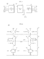
- FIG. 3 is a configuration diagram of an example of a rail-to-rail comparator according to an embodiment
- FIG. 4 is a circuit diagram of the rail-to-rail comparator illustrated in FIG. 3 ;
- FIG. 5 is a configuration diagram of an example of a PAM receiver according to another embodiment
- FIG. 6 is a circuit diagram of the comparison circuit illustrated in FIG. 5 ;
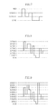
- FIG. 7 is a diagram illustrating the voltage ranges of input signals in a 4-PAM receiver
- FIG. 8 is a diagram illustrating the voltage ranges of input is signals in an 8-PAM receiver
- FIG. 9 is a diagram illustrating the voltage ranges of an input signals in a 10-PAM receiver
- FIG. 10 is a table illustrating the output operation of the comparison circuit based on differential input signals and differential reference voltages in the 4-PAM receiver.
- FIG. 11 is a configuration diagram of an example of a PAM communication system according to another embodiment.
- FIG. 3 is a configuration diagram of an example of a rail-to-rail comparator according to an embodiment.
- the rail-to-rail comparator 10 may include a first comparison unit 12 , a second comparison unit 14 , and an output unit 16 .
- the output unit 16 may be connected between the first and second comparison units 12 and 14 , respectively, as illustrated in FIG. 3 .
- the first comparison unit 12 may be connected to a power supply voltage terminal VDD, and configured to provide a comparison result between differential input signals INP and INN, and differential reference voltages REF 1 and REF 2 to the output unit 16 .
- the second comparison unit 14 may be connected is to a power supply voltage terminal VDD, and configured to provide a comparison result between the differential input signals INP and INN and the differential reference voltages REF 1 and REF 2 to the output unit 16 .
- the output unit 16 may be driven in response to a clock signal CLK, and configured to output complementary output signals OUTP and OUTN as digital signals at a high or low logic voltage level according to the comparison results provided from the first and second comparison units 12 and 14 .
- the first comparison unit 12 may compare the differential input signals INP and INN having a first voltage range to the differential reference voltages REF 1 and REF 2
- the second comparison unit 14 may compare the differential input signals INP and INN having a second voltage range to the differential reference voltages REF 1 and REF 2 .
- the first voltage range may be set to 0 ⁇ (1/2)VDD
- the second voltage range may be set to (1/2)VDD ⁇ VDD. Therefore, even when the levels of the differential input signals INP and INN and/or the differential reference voltage REF 1 and REF 2 are lower than the threshold voltages of the amplifies forming the comparison units 12 and 14 , the first comparison unit 12 may operate to accurately determine the input signal level.
- the first comparison unit 12 may be configured as a first-type differential amplifier, for example, a PMOS differential amplifier
- the second comparison unit 14 may be is configured as a second-type differential amplifier, for example, an NMOS differential amplifier.
- the differential input signals INP and INN and the differential reference voltages REF 1 and REF 2 may be provided to the first and second comparison units 12 and 14 , respectively, at the same time or substantially the same time. According to the levels of the differential input signals INP and INN and the differential reference voltages REF 1 and REF 2 , the first and second comparison units 12 and 14 , respectively, may operate to perform the comparison and amplification operation.
- any one of the comparison units may maintain a turn-off state according to the levels of the differential input signals INP and INN and the differential reference voltages REF 1 and REF 2 . As a result, only one comparison unit may operate.
- the comparison and amplification result of the first or second comparison unit 12 or 14 may be latched by the output unit 16 , and then provided as the output signals OUTP and OUTN in response to the clock signal CLK.
- FIG. 4 is a circuit diagram of the rail-to-rail comparator illustrated in FIG. 3 .
- the output unit 26 may be connected between the first and second comparison units 22 and 24 , respectively, as illustrated in FIG. 4 .
- the first comparison unit 22 may include a first comparator 221 configured to compare a first input signal INP to a first reference voltage REF 1 , and a second comparator 223 configured to compare a second input signal INN to a second reference voltage REF 2 .
- the first and second comparators 221 and 223 may be configured as PMOS amplifiers. Accordingly, even when the input signals INP and INN having the first voltage range of 0 to (1/2)VDD and the reference voltages REF 1 and REF 2 are applied, the first and second comparators 221 and 223 may operate to control the amount of current flowing into the output unit 26 .
- the second comparison unit 24 may include a third comparator 241 configured to compare the first input signal INP to the first reference voltage REF 1 and a fourth comparator 243 configured to compare the second input signal INN to the second reference voltage REF 2 , in order to control the amount of current flowing into the output unit 26 .
- the output unit 26 may include first and second latches 261 and 263 , respectively.
- the first latch 261 may be connected between the first comparator 221 and the third comparator 241 and configured to output a first output signal OUTP.
- the second latch 263 may be connected between the second comparator 223 and the fourth comparator 243 and configured to output a second output signal OUTN.
- the first and second latches 261 and 263 may perform a reset/regenerative operation according to the phase of the clock signal CLK.
- the first latch 261 may be driven by the clock signal CLK and the inverted clock signal /CLK, and may generate the first output signal OUTP according to the amount of current induced in a first output node OUTP.
- the second latch 263 may be driven by the clock signal CLK and the inverted signal /CLK, and may generate the second output signal OUTN according to the amount of current induced in a second output node OUTN.
- the first and second output signals OUTP and OUTN may be outputted as complementary signals at a high or low logic voltage level.
- the rail-to-rail comparator 20 may further include precharge units 28 A and 28 B.
- the precharge units 28 A and 28 B may reset the output signals OUTP and OUTN to a designated voltage level, desirably, (1/2)VDD, when the clock signal CLK has a reset phase.
- the rail-to-rail comparator 20 may be characterized in that, even when the levels of the input signals INP and INN and the reference signals REF 1 and REF 2 may be lower than the threshold voltages of the amplifiers, the first comparison unit 22 may operate to perform a comparison and amplification operation. Therefore, the rail-to-rail comparator 20 may compare input signals in all voltage ranges to the reference voltages, and output the results as digital values.
- first and second comparison units 22 and 24 may be configured in a complementary manner
- the first and second comparison units 22 and 24 may is perform comparison operations according to the voltage levels of the input signals. Therefore, the comparison operations may be performed in a relatively wide input range.
- the comparison operation between the input signals and the reference voltages may be performed based on CMOS logic that has no current consumption. Therefore, it is possible to secure a low power characteristic.
- the rail-to-rail receiver may be applied to a PAM receiver, and the configuration will be described as follows.
- FIG. 5 is a configuration diagram of an example of a PAM receiver according to an embodiment.
- the PAM receiver 30 may include a comparison circuit 32 , a decoder 34 , and an output circuit 36 .
- the comparison circuit 32 may be configured to compare differential input signals INP and INN to differential reference voltages REF 1 and REF 2 , and output the comparison result as a thermometer code.
- the PAM receiver 30 may be configured as an M-PAM receiver.
- the comparison circuit 32 may include (M ⁇ 1) comparators configured to compare the pair of differential input signals INP and INN to (M ⁇ 1) differential reference voltages, respectively.
- each of the (M ⁇ 1) comparators may include the rail-to-rail comparator 10 or 20 illustrated in FIG. 3 or 4 .
- the decoder 34 may be configured to restore the signal is outputted from the comparison circuit 32 into a data signal
- the output circuit 36 may be configured to amplify the binary signal outputted from the decoder 34 and output the amplified signal as a data signal DOUT.
- the decoder 34 may include thermometer-to-binary logic that converts a thermometer code into binary data, but is not limited thereto.
- FIG. 6 is a circuit diagram of the comparison circuit illustrated in FIG. 5 .
- the comparison circuit 40 may include a comparator module 42 , a latch module 44 , and a buffer module 46 .
- the comparator module 42 may include (M ⁇ 1) rail-to-rail comparators 421 configured to compare the differential input signals INP and INN to (M ⁇ 1) differential reference voltages REF 1 _ 1 to REF 1 _(M ⁇ 1) and REF 2 _ 1 to REF 2 _(M ⁇ 1).
- Each of the rail-to-rail comparators 421 may include the comparator 10 or 20 illustrated in FIG. 3 or 4 , respectively. Therefore, even when the potential of the input signals INP and INN is lower than the threshold voltage of the amplifiers, the amplifiers are not turned off while performing the comparison and amplification to operation.
- the output signals of the comparators 421 forming the comparator module 42 may be inputted to latches of the latch module 44 , respectively, and then stabilized, and may output signals of the latch module 44 which are provided to buffers of the buffer module 46 , respectively, and then may be outputted as digital codes, for example, thermometer codes OUT 1 to OUT(M ⁇ 1).
- FIG. 7 is a diagram illustrating the voltage ranges of input signals in a 4-PAM receiver.
- input signals may have four voltage levels in the range of 0 to VDD.
- FIG. 7 illustrates a case in which signals inputted to the 4-PAM receiver have voltage levels of 0, (1/3)VDD, (2/3)VDD, and VDD.
- (M ⁇ 1) differential reference voltages i.e., three differential reference voltages may be set to a value between 0 and (1/3)VDD, a value between (1/3)VDD and (2/3)VDD, and a value between (2/3)VDD and VDD, respectively.
- the CMOS dynamic comparator illustrated in FIG. 2 may not operate because the amplifiers are not turned on. However, since the rail-to-rail comparator according to an embodiment includes the PMOS comparator, a low-level input signal may be sufficiently detected.
- FIG. 8 is a diagram illustrating the voltage ranges of input signals in an 8-PAM receiver.
- the 8-PAM receiver may receive input signals at any one voltage level of 0, (1/7)VDD, (2/7)VDD, (3/7)VDD, (4/7)VDD, (5/7)VDD, (6/7)VDD, and (7/7)VDD or VDD.
- differential reference voltages may be decided as values between the respective input signal levels, and compared to the input signals.
- the input signals having voltage levels of (1/7)VDD, (2/7)VDD, and (3/7)VDD less than (1/2)VDD may be detected by the PMOS comparator.
- FIG. 9 is a diagram illustrating the voltage ranges of an input signals in a 10-PAM receiver.
- the 10-PAM receiver may receive input signals at any one voltage level of 0, (1/9)VDD, (2/9)VDD, (3/9)VDD, (4/9)VDD, (5/9)VDD, (6/9)VDD, (7/9)VDD, (8/9)VDD, and (9/9)VDD or VDD. Furthermore, a comparison circuit forming the 10-PAM receiver may determine the levels of the input signals using differential reference voltages decided as values between the respective input signal levels.
- the PAM receiver since the PAM receiver according to an embodiment may use the rail-to-rail comparators based on CMOS logic, the PAM receiver may detect input signals in all voltage ranges, and may guarantee system performance and reliability because it has a small power consumption.
- FIG. 10 is a table illustrating the output operation of the comparison circuit based on differential input signals and differential reference voltages in the 4-PAM receiver.
- reference voltages REF 1 _ 1 to REF 1 _ 3 for detecting the levels of the differential input signals IPN and INN are set to (1/6)VDD, (1/2)VDD, and (5/6)VDD, respectively.
- differential reference voltages REF 2 _ 1 to REF 2 _ 3 are set to (5/6)VDD, (1/2)VDD, and (1/6)VDD, respectively.
- the differential output signals OUTP and OUTN of the rail-to-rail comparator 20 illustrated in FIG. 4 may be indicated as shown in FIG. 10 .
- Equation 1 may be modeled from the rail-to-rail comparator 20 illustrated in FIG. 4 .
- ⁇ n represents an electron mobility of an NMOS transistor
- ⁇ p represents a hole mobility of a PMOS transistor
- C ox represents gate oxide capacitance
- W represents a transistor width
- L represents a transistor length
- K n represents a transconductance parameter [ ⁇ A/V*V] of the NMOS transistor
- K p represents a transconductance parameter [ ⁇ A/V*V] of the PMOS transistor
- R on — nmos represents a resistance when the NMOS transistor is turned on to operate in a triode region
- R on — pmos represents resistance when the PMOS transistor is turned on to operate in a triode region
- V th represents a threshold voltage (V TH,NMOS in the case of the NMOS transistor, and V TH,PMOS in the case of the PMOS transistor)
- V INP represents a voltage of the input signal INP
- V INN represents a voltage of the input signal INN
- V REFP represents a voltage of the reference
- the amount of current flowing from the first comparator 221 to the first latch 261 corresponds to the sum of amounts of currents flowing through transistors T 5 and T 6 , and may be expressed as
- the amount of current flowing from the second comparator 223 to the second latch 263 corresponds to the sum of amounts of currents flowing through transistors T 7 and T 8 , and may be expressed as
- the first output signal OUTP becomes K p [(
- )] A.
- the amount of current flowing from the first latch 261 to the third comparator 241 corresponds to the sum of amounts of currents flowing through transistors T 1 and T 2 , may be expressed as V INP ⁇ V TH,NMOS +V REF1 ⁇ V TH,NMOS .
- the amount of current flowing from the second latch 263 to the fourth comparator 243 corresponds to the sum of amounts of currents flowing through is transistors T 3 and T 4 , and may be expressed as V INN ⁇ V TH,NMOS +V REF2 ⁇ V TH,NMOS .
- the final output signal OUT of the rail-to-rail comparator may be decided by the sum of A and B.
- the output signal OUTN may be outputted at a high voltage logic level in case where the sum of current amounts based on the input signal INN and the reference voltage REF 2 is greater than the sum of current amounts based on the input signal INP and the reference voltage REF 1 .
- the output signal OUTN when the final output signal OUT is less than 0, the output signal OUTN may be decided as a high voltage logic level, and the output signal OUTP may be decided as a low voltage logic level. Furthermore, when the final output signal OUT is greater than 0, the output signal OUTN may be decided as a low voltage logic level, and the output signal OUTP may be decided as a high voltage logic level.
- the rail-to-rail comparator may compare input signals in all voltage ranges to the reference signals to decide an output voltage level, and may be usefully applied to a low power system, because it has a small power consumption.
- FIG. 11 is a configuration diagram of an example of a PAM is communication system according to another embodiment.
- the PAM communication system 100 may include a PAM transmitter 110 and a PAM receiver 120 .
- the PAM transmitter 110 may include a PAM driver 112 and a transmitter 114 .
- the PAM driver 112 may be configured to convert an inputted digital signal into a multi-level analog signal
- the transmitter 114 may be configured to transmit the analog signal outputted from the PAM driver 112 through a channel.
- the PAM receiver 120 may include the PAM receiver illustrated in FIGS. 5 and 6 .
- the PAM communication system 100 may be configured as an M-PAM communication system. Furthermore, the PAM transmitter 110 may generate and output signals having any one level of first to M-th levels as a differential signal pair, and the PAM receiver 120 may receive the differential signal pair from the transmitter 110 , compare the received differential signal pair to differential reference voltages, and may generate an output signal. At this time, the differential signal pair and the differential reference voltages may be compared by a comparison circuit which may include a first comparison unit configured to compare the differential signal pair to the differential reference voltages, a second comparison unit configured to compare the differential signal pair to the differential reference voltages, and an output unit driven in response to a clock signal and configured to generate complementary output signals according to the comparison results of the first and second is comparison units.
- a comparison circuit which may include a first comparison unit configured to compare the differential signal pair to the differential reference voltages, a second comparison unit configured to compare the differential signal pair to the differential reference voltages, and an output unit driven in response to a clock signal and configured to generate complementary output signals according to the comparison results of
- the output signal of the output circuit may include a thermometer code.
- the signal outputted from the comparison circuit may be restored into a data signal by a decoder, and then amplified and outputted by an output circuit.
- the decoder may include thermometer-to-binary logic to convert the thermometer code of the output circuit into binary data.
- the communication system including the PAM receiver may restore input signals transmitted from the transmitter using the first and second comparison units having a complementary relationship. Therefore, the communication system may restore input signals in all voltage ranges into original signals.
Landscapes
- Engineering & Computer Science (AREA)
- Computer Networks & Wireless Communication (AREA)
- Signal Processing (AREA)
- Physics & Mathematics (AREA)
- Nonlinear Science (AREA)
- Spectroscopy & Molecular Physics (AREA)
- Manipulation Of Pulses (AREA)
Abstract
Description
Claims (23)
Applications Claiming Priority (2)
| Application Number | Priority Date | Filing Date | Title |
|---|---|---|---|
| KR1020110137481A KR101872310B1 (en) | 2011-12-19 | 2011-12-19 | Rail-to-Rail Comparator and Pulse Amplitude Modulation Receiver and Communication System Using the Same |
| KR10-2011-0137481 | 2011-12-19 |
Publications (2)
| Publication Number | Publication Date |
|---|---|
| US20130156126A1 US20130156126A1 (en) | 2013-06-20 |
| US8908778B2 true US8908778B2 (en) | 2014-12-09 |
Family
ID=48610123
Family Applications (1)
| Application Number | Title | Priority Date | Filing Date |
|---|---|---|---|
| US13/590,282 Active 2033-03-09 US8908778B2 (en) | 2011-12-19 | 2012-08-21 | Rail-to-rail comparator, pulse amplitude modulation receiver, and communication system using the same |
Country Status (2)
| Country | Link |
|---|---|
| US (1) | US8908778B2 (en) |
| KR (1) | KR101872310B1 (en) |
Cited By (2)
| Publication number | Priority date | Publication date | Assignee | Title |
|---|---|---|---|---|
| US20150063417A1 (en) * | 2013-08-30 | 2015-03-05 | Hyundai Motor Company | Temperature sensing circuit for igbt module |
| US11251760B2 (en) | 2020-05-20 | 2022-02-15 | Analog Devices, Inc. | Amplifiers with wide input range and low input capacitance |
Families Citing this family (12)
| Publication number | Priority date | Publication date | Assignee | Title |
|---|---|---|---|---|
| US9571115B1 (en) | 2015-11-13 | 2017-02-14 | International Business Machines Corporation | Analog to digital converter with high precision offset calibrated integrating comparators |
| KR102679071B1 (en) * | 2016-11-24 | 2024-07-01 | 에스케이하이닉스 주식회사 | Buffer circuit, semiconductor appratus and system using the same |
| EP3379274B1 (en) * | 2017-03-23 | 2021-04-28 | Rohde & Schwarz GmbH & Co. KG | Multi-level logic analyzer for analyzing multi-level digital signals and method for operating a multi-level logic analyzer for analyzing multi-level digital signals |
| US11909401B2 (en) | 2019-10-11 | 2024-02-20 | University Of Washington | Input driven self-clocked dynamic comparator |
| CN112636729B (en) * | 2020-12-14 | 2022-12-09 | 重庆百瑞互联电子技术有限公司 | Power dynamic comparator circuit with ultra-low power consumption |
| KR102478277B1 (en) | 2021-06-25 | 2022-12-15 | 고려대학교 산학협력단 | 4 level pulse amplifier modulation receiver |
| CN114337709B (en) * | 2021-12-31 | 2023-07-14 | 湖南国科微电子股份有限公司 | Differential signal receiver |
| KR102636015B1 (en) | 2022-04-11 | 2024-02-08 | 고려대학교 산학협력단 | Pam-8 transceiver using differential mode pam-4 and common mode nrz and transceive method therefor |
| KR102715784B1 (en) * | 2023-04-20 | 2024-10-11 | 고려대학교 산학협력단 | Pam-4 transceiver for capacitive-driven channels capable of cancellation crosstalk and method of operation there of |
| US12206532B1 (en) * | 2023-06-06 | 2025-01-21 | Cadence Design Systems, Inc. | Wireline receiver sampling circuit |
| KR102766806B1 (en) | 2023-07-25 | 2025-02-11 | 고려대학교산학협력단 | Decision feedback equalizer minimizing the number of comparators in decoder and its operation method therof |
| KR102747805B1 (en) * | 2023-08-09 | 2024-12-31 | 고려대학교산학협력단 | Decision feedback equalizer outputting thermometer code and its operation method thereof |
Citations (7)
| Publication number | Priority date | Publication date | Assignee | Title |
|---|---|---|---|---|
| US3735392A (en) * | 1971-12-08 | 1973-05-22 | Bell Telephone Labor Inc | Bipolar analog-to-digital converter with double detection of the sign bit |
| JPH0685570A (en) | 1992-08-31 | 1994-03-25 | Toshiba Corp | Operational amplifier circuit device |
| US20030011426A1 (en) * | 2001-06-29 | 2003-01-16 | Casper Bryan K. | Multi-level receiver circuit with digital output using a variable offset comparator |
| US20040141567A1 (en) * | 2003-01-22 | 2004-07-22 | Fuji Yang | Multi-level pulse amplitude modulation receiver |
| US6970022B1 (en) | 2003-09-18 | 2005-11-29 | Lattice Semiconductor Corporation | Controlled hysteresis comparator with rail-to-rail input |
| US20080174343A1 (en) * | 2007-01-18 | 2008-07-24 | Cha Young-Su | Data receiver and data receiving method |
| US20100309964A1 (en) * | 2007-12-19 | 2010-12-09 | Rambus Inc. | Asymmetric communication on shared links |
Family Cites Families (2)
| Publication number | Priority date | Publication date | Assignee | Title |
|---|---|---|---|---|
| JP2005354266A (en) * | 2004-06-09 | 2005-12-22 | Nec Electronics Corp | Voltage comparator circuit |
| JP5471761B2 (en) * | 2010-04-15 | 2014-04-16 | 富士通株式会社 | Receiver circuit |
-
2011
- 2011-12-19 KR KR1020110137481A patent/KR101872310B1/en active Active
-
2012
- 2012-08-21 US US13/590,282 patent/US8908778B2/en active Active
Patent Citations (7)
| Publication number | Priority date | Publication date | Assignee | Title |
|---|---|---|---|---|
| US3735392A (en) * | 1971-12-08 | 1973-05-22 | Bell Telephone Labor Inc | Bipolar analog-to-digital converter with double detection of the sign bit |
| JPH0685570A (en) | 1992-08-31 | 1994-03-25 | Toshiba Corp | Operational amplifier circuit device |
| US20030011426A1 (en) * | 2001-06-29 | 2003-01-16 | Casper Bryan K. | Multi-level receiver circuit with digital output using a variable offset comparator |
| US20040141567A1 (en) * | 2003-01-22 | 2004-07-22 | Fuji Yang | Multi-level pulse amplitude modulation receiver |
| US6970022B1 (en) | 2003-09-18 | 2005-11-29 | Lattice Semiconductor Corporation | Controlled hysteresis comparator with rail-to-rail input |
| US20080174343A1 (en) * | 2007-01-18 | 2008-07-24 | Cha Young-Su | Data receiver and data receiving method |
| US20100309964A1 (en) * | 2007-12-19 | 2010-12-09 | Rambus Inc. | Asymmetric communication on shared links |
Non-Patent Citations (2)
| Title |
|---|
| Lauri Sumanen et al., A Mismatch Insensitive CMOS Dynamic Comparator for Pipeline A/D Converters, p. 32-35, Helsinki University of Technology, Electronic Circuit Design Laboratory, Finland. |
| Sunghyun Park, Yorgos Palaskas, Ashoke Ravi, Ralph E. Bishop, Michael P. Flynn, A 3.5 GS/s 5-b Flash ADC in 90 nm CMOS, IEEE 2006 Custom Intergrated Circuits Conference (CICC), p. 489-492, University of Michigan, Ann Arbor, Michigan (USA) and Intel Corporation, Hillsboro, Oregon (USA). |
Cited By (2)
| Publication number | Priority date | Publication date | Assignee | Title |
|---|---|---|---|---|
| US20150063417A1 (en) * | 2013-08-30 | 2015-03-05 | Hyundai Motor Company | Temperature sensing circuit for igbt module |
| US11251760B2 (en) | 2020-05-20 | 2022-02-15 | Analog Devices, Inc. | Amplifiers with wide input range and low input capacitance |
Also Published As
| Publication number | Publication date |
|---|---|
| US20130156126A1 (en) | 2013-06-20 |
| KR20130070248A (en) | 2013-06-27 |
| KR101872310B1 (en) | 2018-07-02 |
Similar Documents
| Publication | Publication Date | Title |
|---|---|---|
| US20130156126A1 (en) | Rail-to-rail comparator, pulse amplitude modulation receiver, and communication system using the same | |
| US8624632B2 (en) | Sense amplifier-type latch circuits with static bias current for enhanced operating frequency | |
| US7154294B2 (en) | Comparators capable of output offset calibration | |
| US7646220B2 (en) | Reduced voltage subLVDS receiver | |
| US6885245B2 (en) | Differential amplifier and comparator using the same | |
| US6798243B1 (en) | Apparatus and method for level-shifting input receiver circuit from high external voltage to low internal supply voltage | |
| KR100818796B1 (en) | Data receiver and how to receive data | |
| US7482843B2 (en) | Signal amplifier | |
| Park et al. | A 56-Gb/s PAM-4 receiver using time-based LSB decoder and S/H technique for robustness to comparator voltage variations | |
| JP5334366B2 (en) | Semiconductor integrated circuit | |
| US5894233A (en) | Sense amplifiers including bipolar transistor input buffers and field effect transistor latch circuits | |
| JP2008029004A (en) | Receiving end to reduce channel mutual symbol interference and compensate for signal gain loss | |
| CN1921307B (en) | Dual reference input receiver of semiconductor device and method of receiving input data signal | |
| US7403045B2 (en) | Comparator circuit with reduced switching noise | |
| US9094003B2 (en) | Buffering circuit, semiconductor device having the same, and methods thereof | |
| WO2006126436A1 (en) | Signal converting circuit | |
| US6617899B2 (en) | Ultra high speed clocked analog latch | |
| JP4982830B2 (en) | Semiconductor integrated circuit | |
| US7633318B2 (en) | Data receiver of semiconductor integrated circuit and method for controlling the same | |
| US12470438B2 (en) | Low voltage differential signaling receiver | |
| US11843386B1 (en) | Latched comparator circuitry with reduced clock feedthrough | |
| US20180309450A1 (en) | Voltage conversion circuit and electronic device | |
| US8035420B2 (en) | Semiconductor device and method for operating the same | |
| US20060164144A1 (en) | Flip-flop circuit and semiconductor device | |
| US20240413834A1 (en) | Voltage-to-time converters and methods of operating same |
Legal Events
| Date | Code | Title | Description |
|---|---|---|---|
| AS | Assignment |
Owner name: SK HYNIX INC., KOREA, REPUBLIC OF Free format text: ASSIGNMENT OF ASSIGNORS INTEREST;ASSIGNORS:CHUNG, JIN IL;CHUN, JUN HYUN;YUN, DAE HO;REEL/FRAME:028817/0754 Effective date: 20120705 Owner name: INDUSTRY-UNIVERSITY COOPERATION FOUNDATION SOGANG Free format text: ASSIGNMENT OF ASSIGNORS INTEREST;ASSIGNOR:BURM, JIN WOOK;REEL/FRAME:028817/0795 Effective date: 20120705 |
|
| STCF | Information on status: patent grant |
Free format text: PATENTED CASE |
|
| FEPP | Fee payment procedure |
Free format text: PAYOR NUMBER ASSIGNED (ORIGINAL EVENT CODE: ASPN); ENTITY STATUS OF PATENT OWNER: LARGE ENTITY |
|
| CC | Certificate of correction | ||
| MAFP | Maintenance fee payment |
Free format text: PAYMENT OF MAINTENANCE FEE, 4TH YEAR, LARGE ENTITY (ORIGINAL EVENT CODE: M1551) Year of fee payment: 4 |
|
| MAFP | Maintenance fee payment |
Free format text: PAYMENT OF MAINTENANCE FEE, 8TH YEAR, LARGE ENTITY (ORIGINAL EVENT CODE: M1552); ENTITY STATUS OF PATENT OWNER: LARGE ENTITY Year of fee payment: 8 |
|
| MAFP | Maintenance fee payment |
Free format text: PAYMENT OF MAINTENANCE FEE, 12TH YEAR, LARGE ENTITY (ORIGINAL EVENT CODE: M1553); ENTITY STATUS OF PATENT OWNER: LARGE ENTITY Year of fee payment: 12 |