US8908112B2 - Display panel, display device, and electronic unit - Google Patents
Display panel, display device, and electronic unit Download PDFInfo
- Publication number
- US8908112B2 US8908112B2 US13/440,511 US201213440511A US8908112B2 US 8908112 B2 US8908112 B2 US 8908112B2 US 201213440511 A US201213440511 A US 201213440511A US 8908112 B2 US8908112 B2 US 8908112B2
- Authority
- US
- United States
- Prior art keywords
- display panel
- barrier layer
- transparent conductive
- display
- panel
- Prior art date
- Legal status (The legal status is an assumption and is not a legal conclusion. Google has not performed a legal analysis and makes no representation as to the accuracy of the status listed.)
- Active, expires
Links
Images


Classifications
-
- G—PHYSICS
- G02—OPTICS
- G02B—OPTICAL ELEMENTS, SYSTEMS OR APPARATUS
- G02B30/00—Optical systems or apparatus for producing three-dimensional [3D] effects, e.g. stereoscopic images
- G02B30/20—Optical systems or apparatus for producing three-dimensional [3D] effects, e.g. stereoscopic images by providing first and second parallax images to an observer's left and right eyes
- G02B30/26—Optical systems or apparatus for producing three-dimensional [3D] effects, e.g. stereoscopic images by providing first and second parallax images to an observer's left and right eyes of the autostereoscopic type
- G02B30/30—Optical systems or apparatus for producing three-dimensional [3D] effects, e.g. stereoscopic images by providing first and second parallax images to an observer's left and right eyes of the autostereoscopic type involving parallax barriers
-
- G02B27/2214—
-
- G—PHYSICS
- G02—OPTICS
- G02B—OPTICAL ELEMENTS, SYSTEMS OR APPARATUS
- G02B30/00—Optical systems or apparatus for producing three-dimensional [3D] effects, e.g. stereoscopic images
- G02B30/20—Optical systems or apparatus for producing three-dimensional [3D] effects, e.g. stereoscopic images by providing first and second parallax images to an observer's left and right eyes
- G02B30/26—Optical systems or apparatus for producing three-dimensional [3D] effects, e.g. stereoscopic images by providing first and second parallax images to an observer's left and right eyes of the autostereoscopic type
- G02B30/27—Optical systems or apparatus for producing three-dimensional [3D] effects, e.g. stereoscopic images by providing first and second parallax images to an observer's left and right eyes of the autostereoscopic type involving lenticular arrays
-
- G—PHYSICS
- G02—OPTICS
- G02F—OPTICAL DEVICES OR ARRANGEMENTS FOR THE CONTROL OF LIGHT BY MODIFICATION OF THE OPTICAL PROPERTIES OF THE MEDIA OF THE ELEMENTS INVOLVED THEREIN; NON-LINEAR OPTICS; FREQUENCY-CHANGING OF LIGHT; OPTICAL LOGIC ELEMENTS; OPTICAL ANALOGUE/DIGITAL CONVERTERS
- G02F1/00—Devices or arrangements for the control of the intensity, colour, phase, polarisation or direction of light arriving from an independent light source, e.g. switching, gating or modulating; Non-linear optics
- G02F1/01—Devices or arrangements for the control of the intensity, colour, phase, polarisation or direction of light arriving from an independent light source, e.g. switching, gating or modulating; Non-linear optics for the control of the intensity, phase, polarisation or colour
- G02F1/13—Devices or arrangements for the control of the intensity, colour, phase, polarisation or direction of light arriving from an independent light source, e.g. switching, gating or modulating; Non-linear optics for the control of the intensity, phase, polarisation or colour based on liquid crystals, e.g. single liquid crystal display cells
- G02F1/133—Constructional arrangements; Operation of liquid crystal cells; Circuit arrangements
- G02F1/1333—Constructional arrangements; Manufacturing methods
- G02F1/133308—Support structures for LCD panels, e.g. frames or bezels
- G02F1/133311—Environmental protection, e.g. against dust or humidity
-
- G—PHYSICS
- G02—OPTICS
- G02F—OPTICAL DEVICES OR ARRANGEMENTS FOR THE CONTROL OF LIGHT BY MODIFICATION OF THE OPTICAL PROPERTIES OF THE MEDIA OF THE ELEMENTS INVOLVED THEREIN; NON-LINEAR OPTICS; FREQUENCY-CHANGING OF LIGHT; OPTICAL LOGIC ELEMENTS; OPTICAL ANALOGUE/DIGITAL CONVERTERS
- G02F1/00—Devices or arrangements for the control of the intensity, colour, phase, polarisation or direction of light arriving from an independent light source, e.g. switching, gating or modulating; Non-linear optics
- G02F1/01—Devices or arrangements for the control of the intensity, colour, phase, polarisation or direction of light arriving from an independent light source, e.g. switching, gating or modulating; Non-linear optics for the control of the intensity, phase, polarisation or colour
- G02F1/13—Devices or arrangements for the control of the intensity, colour, phase, polarisation or direction of light arriving from an independent light source, e.g. switching, gating or modulating; Non-linear optics for the control of the intensity, phase, polarisation or colour based on liquid crystals, e.g. single liquid crystal display cells
- G02F1/133—Constructional arrangements; Operation of liquid crystal cells; Circuit arrangements
- G02F1/1333—Constructional arrangements; Manufacturing methods
- G02F1/1335—Structural association of cells with optical devices, e.g. polarisers or reflectors
- G02F1/133509—Filters, e.g. light shielding masks
- G02F1/133512—Light shielding layers, e.g. black matrix
-
- G02F2001/133311—
-
- H—ELECTRICITY
- H04—ELECTRIC COMMUNICATION TECHNIQUE
- H04N—PICTORIAL COMMUNICATION, e.g. TELEVISION
- H04N2213/00—Details of stereoscopic systems
- H04N2213/001—Constructional or mechanical details
Definitions
- the present disclosure relates to a display panel capable of multi-view display allowing viewing of two-dimensional (2D) image (planar image) that looks different depending on from which perspective the image is viewed, or capable of three-dimensional (3D) display allowing viewing of 3D image (stereoscopic image) from a specific perspective, and to a display device provided with such a display panel.
- the present disclosure also relates to an electronic unit provided with the display device as above.
- a display device capable of multi-view display or 3D display has been recently in practical use.
- Such a display device is known to include a barrier layer on the display region of a display panel, for example.
- a barrier layer Japanese Unexamined Patent Application Publication No. 9-281440 describes a barrier layer including a plurality of transmissive slits each separated by a light-shielding region.
- Japanese Unexamined Patent Application Publication No. 8-106070 describes a barrier liquid crystal display with which a light-shielding region is generated in response to application of a voltage to a liquid crystal material.
- the display panel as above shows display anomalies in some cases upon application of a high electric potential such as static electricity from the outside.
- a high electric potential such as static electricity from the outside.
- This disadvantage becomes apparent especially when the display panel includes electrodes only on one of substrates because this easily leads to accumulation of electric charge, e.g., static electricity, on the remaining substrate side.
- Japanese Unexamined Patent Application Publication No. 2010-204406 describes an approach to configure a barrier layer by metal to provide the resulting barrier layer with the capability of shielding against static electricity.
- a display panel being both anti-static and resistant to corrosion, a display device provided with the display panel, and an electronic unit provided with the display device.
- a display panel includes a panel section, a barrier layer, and a transparent conductive layer.
- the panel section includes a plurality of pixels arranged in a matrix.
- the barrier layer is provided at an upper or lower part of the panel section, and includes a light-shielding region and transmissive regions that are arranged systematically.
- the transparent conductive layer is provided at the upper part of the panel section.
- a display device includes a display panel, and a chassis supporting the display panel.
- the display panel includes a panel section including a plurality of pixels arranged in a matrix; a barrier layer provided at an upper or lower part of the panel section, and the barrier layer including light-shielding regions and transmissive regions that are arranged systematically; and a transparent conductive layer provided at the upper part of the panel section.
- An electronic unit includes a display device including a display panel and a chassis supporting the display panel.
- the display panel includes a panel section including a plurality of pixels arranged in a matrix; a barrier layer provided at an upper or lower part of the panel section, and the barrier layer including light-shielding regions and transmissive regions that are arranged systematically; and a transparent conductive layer provided at the upper part of the panel section.
- the transparent conductive layer is provided at the upper portion of the panel section. This configuration allows to select each suitable material for the barrier layer and for the transparent conductive layer, thereby being able to provide the resistance to corrosion by water to each of the barrier layer and the transparent conductive layer.
- the display panel may be additionally provided with a conductor electrically connecting together the transparent conductive layer and a conductive member.
- the panel section may be provided with a first substrate including the conductive member, or the display panel may include the conductive member at the upper-surface end portion thereof.
- the transparent conductive layer is an adhesive layer, for example.
- the display panel may be provided with a polarizing plate being in contact with the transparent conductive layer, and the panel section may include a liquid crystal layer.
- the display panel may be provided with a transparent substrate being in contact with the transparent conductive layer, and the panel section may include a light-emitting layer.
- the display panel may include a substrate between the transparent conductive layer and the panel section, and the transparent conductive layer may be an anti-reflection layer.
- the substrate may be a polarizing plate or a transparent substrate.
- the transparent conductive layer is provided at the upper portion of the panel section separately from the barrier layer, thereby being able to provide the resistance to corrosion by water to each of the barrier layer and the transparent conductive layer. This accordingly prevents the resulting structure from being electrically charged and corrosive.
- FIG. 1 is a view of a display device in a first embodiment, showing an exemplary cross-sectional configuration thereof.
- FIG. 2 is a view of a panel section and that of a barrier layer at the time of dual viewing, showing an exemplary cross-sectional configuration thereof.
- FIG. 3 is a view of the panel section and that of the barrier layer at the time of 3D display, showing an exemplary cross-sectional configuration thereof.
- FIG. 4 is a cross-sectional view of the display device of FIG. 1 in Modification 1-1.
- FIG. 5 is a cross-sectional view of the display device of FIG. 1 in Modification 1-2.
- FIG. 6 is a cross-sectional view of the display device of FIG. 1 in Modification 1-3.
- FIG. 7 is a cross-sectional view of the display device of FIG. 1 in Modification 1-4.
- FIG. 8 is a cross-sectional view of the display device of FIG. 1 in Modification 1-5.
- FIG. 9 is a cross-sectional view of the display device of FIG. 1 in Modification 1-6.
- FIG. 10 is a cross-sectional view of the display device of FIG. 1 in Modification 1-7.
- FIG. 11 is a cross-sectional view of the display device of FIG. 1 in Modification 1-8.
- FIG. 12 is a view of a display device in a second embodiment, showing an exemplary cross-sectional configuration thereof.
- FIG. 13 is a cross-sectional view of the display device of FIG. 12 in Modification 2-1.
- FIG. 14 is a cross-sectional view of the display device of FIG. 12 in Modification 2-2.
- FIG. 15 is a cross-sectional view of the display device of FIG. 12 in Modification 2-3.
- FIG. 16 is a perspective view of an exemplary electronic unit in an application example.
- Second Embodiment Organic EL (Electro-Luminescence) Display Device
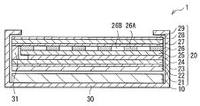
- FIG. 1 is a view of a display device 1 of a first embodiment, showing an exemplary cross-sectional configuration thereof. Note that FIG. 1 is a schematic view, and the dimension and shape thereof are not necessarily the same as those in reality.
- the display device 1 is configured to include a display panel 20 , a backlight 10 , and a chassis 30 .
- the backlight 10 is disposed behind the display panel 20 , and the chassis 30 supports the display panel 20 and the backlight 10 .
- the backlight 10 is a plane-emitting light source that illuminates the display panel 20 from the rear thereof.
- the upper surface of the display panel 20 serves as an image display surface
- the chassis 30 has an aperture to correspond at least to the image display surface.
- a frame portion forming the aperture as such is made conductive, for example, and the chassis 30 including the frame portion is preferably made conductive in its entirety. Note that, in the first embodiment, the chassis 30 may be made nonconductive.
- the display panel 20 is a transmissive panel in which pixels (not shown) are driven according to an image signal coming from the outside.
- the display panel 20 includes a panel section, i.e., corresponding to a panel section 40 that will be described later, including a liquid crystal layer 24 sandwiched between a pair of substrates, i.e., lower and upper substrates 23 and 25 .
- the lower substrate 23 is a so-called TFT (Thin Film Transistor) substrate, and includes a common wiring for electrical connection with a conductor 31 that will be described later.
- the common wiring is the one to be at a ground potential when the display device 1 is in use.
- the upper substrate 25 is a so-called CF (Color Filter) substrate.
- the display panel 20 includes an adhesive layer 22 and a polarizing plate 21 at the lower portion of the panel section, i.e., on the lower substrate 23 side.
- the polarizing plate 21 is fixed to the lower substrate 23 via the adhesive layer 22 .
- the display panel 20 is provided with a barrier layer 26 at the upper portion of the panel section, i.e., on the upper substrate 25 side, as shown in FIG. 1 , for example.
- the barrier layer 26 is formed directly on the upper surface of the upper substrate 25 , for example.
- the barrier layer 26 may be configured by a glass substrate (not shown) formed with the barrier layer 26 , and the resulting structure may be affixed onto the upper surface of the upper substrate 25 .
- the display panel 20 is provided also with an adhesive layer 27 , a polarizing plate 28 , and an AR (Anti-Reflection) layer 29 as shown in FIG. 1 , for example.
- the polarizing plate 28 is fixed to the upper substrate 25 via the adhesive layer 27 .
- the AR layer 29 is formed by a coating process on the polarizing plate 28 , the AR layer 29 is in directly contact with the polarizing plate 28 .
- the AR layer 29 is made of a film, the AR layer 29 is fixed to the polarizing plate 28 via any other adhesive layer that is not shown, for example. Note that, in the embodiment, if appropriate, the AR layer 29 may not be provided.
- the adhesive layer 27 serves not only to fix together the polarizing plate 28 and the barrier layer 26 , but also to pass light therethrough and is made conductive.
- the adhesive layer 27 is also resistant to corrosion by water.
- the adhesive layer 27 is made of an adhesive containing the needle-shaped ITO (Indium-Tin Oxide) as described in Japanese Unexamined Patent Application Publication No. 7-153313.
- the display panel 20 also includes the conductor 31 as shown in FIG. 1 , for example.
- the conductor 31 is for preventing accumulation of electric charge such as static electricity on the upper substrate 25 side of the display panel 20 .
- the conductor 31 electrically connects together the adhesive layer 27 being conductive and the common wiring on the lower substrate 23 , and is configured by pillar-like metal, for example.
- the display panel 20 is a display panel capable of multi-view display allowing viewing of 2D image (planar image) that looks different depending on from which perspective the image is viewed, or capable of 3D display allowing viewing of 3D image (stereoscopic image) from a specific perspective.
- FIG. 2 is a diagram schematically showing how multi-view display is made on the display panel 20 .
- FIG. 3 is a diagram schematically showing how 3D display is made on the display panel 20 .
- the panel section 40 including the liquid crystal layer 24 sandwiched between the lower and upper substrates 23 and 25 is provided with a display region as shown in FIGS. 2 and 3 , for example.
- the display region includes a plurality of pixels 42 arranged in a matrix.
- the pixels 42 are each capable of emitting light of various colors, and each include two sub-pixels 41 for each color, for example.
- the sub-pixels 41 are each capable of emitting light of red, green, or blue, for example.
- the pixels 42 are each including two sub-pixels 41 R for red, two sub-pixels 41 G for green, and two sub-pixels 41 B for blue, for example.
- the sub-pixels 41 in each of the pixels 42 as such are arranged in stripes, for example. Between the pixels 42 or between the sub-pixels 41 , a black section 43 being a light-shielding section is each disposed.
- the black section 43 is in the shape of a grid in the plane, for example.
- the barrier layer 26 is for shielding a part of the light (image light) coming from each of the pixels 42 of the panel section 40 .
- the barrier layer 26 shields a part of the pixels 42 , thereby allowing viewing of 2D image (planar image) that looks different depending on from which appropriate-viewing direction a viewer H looks, i.e., direction d 1 or d 2 that will be described later (see FIG. 2 ).
- the display device 1 operates as a so-called dual-view display device.
- the barrier layer 26 shields a part of the pixels 42 , thereby allowing viewing of 2D image (planar image) that looks different between right and left eyes e 1 and e 2 (see FIG. 3 ) of the viewer H.
- the display device 1 operates as a so-called 3D display device.
- the barrier layer 26 is disposed at the position opposing to the panel section 40 .
- the barrier layer 26 is in such a barrier pattern as exemplarily shown in FIGS. 2 and 3 , i.e., a barrier pattern of including a plurality of transmissive regions 26 B that are arranged two-dimensionally, and including a light-shielding region 26 A around each of the transmissive regions 26 B.
- the barrier layer 26 is resistant to corrosion by water.
- the light-shielding regions 26 A are each configured by a light-shielding member, for example. Such a light-shielding member is exemplified by a resin containing a black pigment or others.
- the transmissive regions 26 B are each an aperture.
- the transmissive regions 26 B as such are arranged systematically, and are arranged two-dimensionally in the row and column directions.
- the light-shielding regions 26 A and the transmissive regions 26 B are arranged in a checkered pattern, i.e., alternately in the row and column directions, for example.
- the barrier layer 26 is so disposed as to make entirely or partially visible any predetermined sub-pixel 41 via each corresponding transmissive region 26 B when the viewer H looks at the display panel 20 from the first appropriate-view direction d 1 as shown in FIG. 2 , for example. Also at the time of dual-view display, the barrier layer 26 is so disposed as to make entirely or partially visible any other sub-pixel 41 via each corresponding transmissive region 26 B when the viewer H looks at the display panel 20 from the second appropriate-view direction d 2 as shown in FIG. 2 , for example.
- the transmissive regions 26 B are each so configured as to allow entire or partial viewing of different sub-pixels 41 therethrough depending on from which appropriate-view direction, i.e., the first or second appropriate-view direction d 1 or d 2 , the viewer H looks at the display panel 20 , for example. Therefore, when looking at the display panel 20 from the first or second appropriate-view direction d 1 or d 2 , the viewer H is allowed to view the sub-pixels 41 of three colors RGB for each of the pixels 42 , for example.
- the barrier layer 26 is so disposed as to make entirely or partially visible any predetermined sub-pixel 41 via each corresponding transmissive region 26 B when the viewer H looks at the display panel 20 using his or her right eye e 1 as shown in FIG. 3 , for example. Also at the time of 3D display, the barrier layer 26 is so disposed as to make entirely or partially visible any other sub-pixel 41 via each corresponding transmissive region 26 B when the viewer H looks at the display panel 20 using his or her left eye e 2 as shown in FIG. 3 , for example.
- the transmissive regions 26 B are each so configured as to allow entire or partial viewing of different sub-pixels 41 therethrough depending on which eye, i.e., the right or left eye e 1 or e 2 , the viewer H uses to look at the display panel 20 , for example. Therefore, when looking at the display panel 20 using his or her right or left eye e 1 or e 2 , the viewer H is allowed to view the sub-pixels 41 of three colors RGB for each of the pixels 42 , for example.
- light coming from the backlight 10 is modulated by each of the pixels 42 of the panel section 40 , and then any predetermined image light is provided to the barrier layer 26 . Thereafter, the image light is partially shielded by the light-shielding regions 26 A of the barrier layer 26 , and the remaining light passed through the transmissive regions 26 B is emitted from the image display surface of the display panel 20 .
- the barrier layer 26 is in a mode for dual-view display, for example, the light emitted from the image display surface forms an image at a predetermined position (perspective) on the line segment parallel to the first appropriate-view direction d 1 , thereby generating 2D image (planar image).
- the light emitted from the image display surface forms an image at a predetermined position (perspective) on the line segment parallel to the second appropriate-view direction d 2 , thereby generating 2D image (planar image), for example.
- the barrier layer 26 is in a mode for 3D display, for example, the light emitted from the image display surface forms an image at the position (perspective) of the right eye e 1 , thereby generating 2D image (planar image).
- the light emitted from the image display surface forms an image at the position (perspective) of the left eye e 2 , thereby generating 2D image (planar image), for example.
- the viewer H is allowed to view 3D image.
- the adhesive layer 27 as a transparent conductive layer is provided at the upper portion of the panel section 40 .
- This configuration allows to select each suitable material for the barrier layer 26 and for the adhesive layer 27 , thereby providing the resistance to corrosion by water to each of the barrier layer 26 and the adhesive layer 27 .
- the light-shielding regions 26 A may be each made of a resin containing a black pigment or others
- the transmissive regions 26 B may be each formed like an aperture
- the adhesive layer 27 may be made of an adhesive containing the needle-shaped ITO described above.
- the barrier layer 26 since the barrier layer 26 is not configured by a metal thin film that is highly corrosive by water, the resulting display panel 20 favorably becomes both anti-static and resistant to corrosion.
- the conductor 31 is configured by the pillar-like metal, but alternatively, the conductor 31 may be made of a metal paste, for example.
- the conductor 31 may possibly be disposed on the side surface of the display panel 20 as shown in FIG. 4 , for example. If this is the configuration, the conductor 31 electrically connects together the end portion of the adhesive layer 27 and the common wiring on the lower substrate 23 .
- the adhesive layer 27 is made conductive, but alternatively, the AR layer 29 may be made conductive, for example.
- the conductor 31 is disposed at the upper-surface end portion of the display panel 20 , i.e., at the upper-surface end portion of the AR layer 29 , and electrically connects together the chassis 30 and the AR layer 29 as shown in FIG. 5 , for example.
- the conductor 31 may be configured by pillar-like metal, or may be made of a metal paste. This accordingly prevents accumulation of electric charge such as static electricity on the upper substrate 25 side of the display panel 20 . Accordingly, similarly to the first embodiment described above, the resulting display panel 20 successfully becomes both anti-static and resistant to corrosion.
- the conductor 31 is provided at the upper-surface end portion of the display panel 20 , but alternatively, the conductor 31 may be provided on the side surface of the display panel 20 as shown in FIG. 6 , for example. If this is the configuration, however, the conductor 31 is preferably made of a metal paste.
- the barrier layer 26 is provided on the upper substrate 25 , but alternatively, the barrier layer 26 may be provided below the lower substrate 23 , for example. Specifically, the barrier layer 26 may be formed below the lower substrate 23 to be in contact therewith as shown in FIG. 7 , for example.
- the adhesive layer 22 is preferably in the configuration similar to that of the adhesive layer 27 .
- the adhesive layer 22 serves not only to fix together the polarizing plate 21 and the barrier layer 26 , but also to pass light therethrough and is made conductive.
- the adhesive layer 22 is also resistant to corrosion by water.
- the adhesive layer 22 is made of an adhesive containing the needle-shaped ITO as described in Japanese Unexamined Patent Application Publication No. 7-153313, for example.
- the display panel 20 is additionally provided with a conductor 32 , which electrically connects together the adhesive layer 22 and the chassis 30 as shown in FIG. 8 , for example. If this is the configuration, any electric charge such as static electricity is prevented from accumulating not only on the upper substrate 25 of the display panel 20 but also on the lower substrate 23 side thereof. Accordingly, similarly to the first embodiment described above, the resulting display panel 20 successfully becomes both anti-static and resistant to corrosion.
- the adhesive layer 22 is preferably in the configuration similar to that of the adhesive layer 27 .
- the adhesive layer 22 serves not only to fix together the polarizing plate 21 and the barrier layer 26 , but also to pass light therethrough and is made conductive.
- the adhesive layer 22 is also resistant to corrosion by water.
- the adhesive layer 22 is made of an adhesive containing the needle-shaped ITO as described in Japanese Unexamined Patent Application Publication No. 7-153313, for example.
- the display panel 20 is additionally provided with the conductor 32 , which electrically connects together the adhesive layer 22 and the chassis 30 as shown in FIG. 9 , for example. If this is the configuration, any electric charge such as static electricity is prevented from accumulating not only on the upper substrate 25 of the display panel 20 but also on the lower substrate 23 side thereof. Accordingly, similarly to the first embodiment described above, the resulting display panel 20 successfully becomes both anti-static and resistant to corrosion.
- the adhesive layer 22 is preferably in the configuration similar to that of the adhesive layer 22 of Modification 1-6 described above.
- the display panel 20 is additionally provided with the conductor 32 , which electrically connects together the adhesive layer 22 and the chassis 30 as shown in FIG. 10 , for example. If this is the configuration, any electric charge such as static electricity is prevented from accumulating not only on the upper substrate 25 of the display panel 20 but also on the lower substrate 23 side thereof. Accordingly, similarly to Modification 1-2 described above, the resulting display panel 20 successfully becomes both anti-static and resistant to corrosion.
- the adhesive layer 22 is preferably in the configuration similar to that of the adhesive layer 22 of Modification 1-6 described above.
- the display panel 20 is additionally provided with the conductor 32 , which electrically connects together the adhesive layer 22 and the chassis 30 as shown in FIG. 11 , for example. If this is the configuration, any electric charge such as static electricity is prevented from accumulating not only on the upper substrate 25 of the display panel 20 but also on the lower substrate 23 side thereof. Accordingly, similarly to Modification 1-3 described above, the resulting display panel 20 successfully becomes both anti-static and resistant to corrosion.
- FIG. 12 is a view of a display device 2 in a second embodiment, showing an exemplary cross-sectional configuration thereof. Note that FIG. 12 is a schematic view, and the dimension and shape thereof are not necessarily the same as those in reality.
- the display device 2 is configured to include a display panel 50 , and the chassis 30 supporting the display panel 50 .
- any structure component same as that of the first embodiment described above is provided with the same reference numeral.
- the display panel 50 is a self-emitting panel in which pixels (not shown) are driven according to an image signal coming from the outside.
- the display panel 50 includes a panel section (corresponding to the panel section 40 in the first embodiment described above) including an organic EL layer 52 sandwiched between a pair of substrates, i.e., lower and upper substrates 51 and 53 .
- the lower substrate 51 is a so-called TFT substrate, and includes a common wiring for electrical connection with the conductor 31 .
- the common wiring is the one to be at a ground potential when the display device 2 is in use.
- the upper substrate 53 is a transparent substrate such as glass substrate.
- the display panel 50 includes the barrier layer 26 at the upper portion of the panel section, i.e., on the upper substrate 53 side.
- the barrier layer 26 is formed directly on the upper surface of the upper substrate 53 , for example.
- the barrier layer 26 may be configured by a glass substrate (not shown) formed with the barrier layer 26 , and the resulting structure may be affixed onto the upper surface of the upper substrate 53 .
- the display panel 50 is provided also with the adhesive layer 27 , a support substrate 54 , and the AR (Anti-Reflection) layer 29 as shown in FIG. 12 , for example.
- the support substrate 54 is fixed to the upper substrate 53 via the adhesive layer 27 , and is a glass substrate, for example.
- the AR layer 29 is formed by a coating process on the support substrate 54 , the AR layer 29 is in directly contact with the support substrate 54 .
- the AR layer 29 is made of a film, the AR layer 29 is fixed to the support substrate 54 via any other adhesive layer that is not shown, for example. Note that, in this second embodiment, if appropriate, the AR layer 29 may not be provided.
- the adhesive layer 27 serves not only to fix together the support substrate 54 and the barrier layer 26 , but also to pass light therethrough and is made conductive.
- the adhesive layer 27 is also resistant to corrosion by water.
- the adhesive layer 27 is made of an adhesive containing the needle-shaped ITO (Indium-Tin Oxide) as described in Japanese Unexamined Patent Application Publication No. 7-153313.
- the display panel 50 also includes the conductor 31 as shown in FIG. 12 , for example.
- the conductor 31 is for preventing accumulation of electric charge such as static electricity on the upper substrate 53 side of the display panel 50 .
- the conductor 31 electrically connects together the adhesive layer 27 being conductive and the common wiring on the lower substrate 51 , and is configured by pillar-like metal, for example.
- the display panel 50 is a display panel capable of multi-view display or 3D display similarly to the display panel 20 in the first embodiment described above.
- the panel section 40 including the organic EL layer 52 sandwiched between the lower and upper substrates 51 and 52 is provided with a display region as shown in FIGS. 2 and 3 , for example.
- the display region includes a plurality of pixels 42 arranged in a matrix.
- the barrier layer 26 is for shielding a part of the light (image light) coming from each of the pixels 42 of the panel section 40 .
- the barrier layer 26 shields a part of the pixels 42 , thereby allowing viewing of 2D image (planar image) that looks different depending on from which appropriate-viewing direction the viewer H looks, i.e., the direction d 1 or d 2 that will be described later (see FIG. 2 ).
- the display device 2 operates as a so-called dual-view display device.
- the barrier layer 26 shields a part of the pixels 42 , thereby allowing viewing of 2D image (planar image) that looks different between the right and left eyes e 1 and e 2 (see FIG. 3 ) of the viewer H.
- the display device 2 operates as a so-called 3D display device.
- image light coming from each of the pixels 42 enters the barrier layer 26 . Thereafter, the image light is partially shielded by the light-shielding regions 26 A of the barrier layer 26 , and the remaining light passed through the transmissive regions 26 B is emitted from the image display surface of the display panel 50 .
- the barrier layer 26 is in a mode for dual-view display, for example, the light emitted from the image display surface forms an image at a predetermined position (perspective) on the line segment parallel to the first appropriate-view direction d 1 , thereby generating 2D image (planar image).
- the light emitted from the image display surface forms an image at a predetermined position (perspective) on the line segment parallel to the second appropriate-view direction d 2 , thereby generating 2D image (planar image), for example.
- the barrier layer 26 is in a mode for 3D display, for example, the light emitted from the image display surface forms an image at the position (perspective) of the right eye e 1 , thereby generating 2D image (planar image).
- the light emitted from the image display surface forms an image at the position (perspective) of the left eye e 2 , thereby generating 2D image (planar image), for example.
- the viewer H is allowed to view 3D image.
- the adhesive layer 27 as a transparent conductive layer is provided at the upper portion of the panel section 40 .
- This configuration allows to select each suitable material for the barrier layer 26 and for the adhesive layer 27 , thereby providing the resistance to corrosion by water to each of the barrier layer 26 and the adhesive layer 27 .
- the light-shielding regions 26 A may be each made of a resin containing a black pigment or others
- the transmissive regions 26 B may be each formed like an aperture
- the adhesive layer 27 may be made of an adhesive containing the needle-shaped ITO described above.
- the barrier layer 26 is not configured by a metal thin film that is highly corrosive by water, the resulting display panel 50 favorably becomes both anti-static and resistant to corrosion.
- the conductor 31 is configured by the pillar-like metal, but alternatively, the conductor 31 may be made of a metal paste, for example.
- the conductor 31 may possibly be disposed on the side surface of the display panel 50 as shown in FIG. 13 , for example. If this is the configuration, the conductor 31 electrically connects together the end portion of the adhesive layer 27 and the common wiring on the lower substrate 51 .
- the adhesive layer 27 is made conductive, but alternatively, the AR layer 29 may be made conductive, for example.
- the conductor 31 is provided on the upper-surface end portion of the display panel 50 , i.e., at the upper-surface end portion of the AR layer 29 , and electrically connects together the chassis 30 and the AR layer 29 .
- the conductor 31 may be configured by pillar-like metal, or may be made of a metal paste. This accordingly prevents accumulation of electric charge such as static electricity on the upper substrate 53 side of the display panel 50 . Accordingly, similarly to the second embodiment described above, the resulting display panel 50 successfully becomes both anti-static and resistant to corrosion.
- the conductor 31 is provided at the upper-surface end portion of the display panel 50 , but alternatively, the conductor 31 may be provided on the side surface of the display panel 50 as shown in FIG. 15 , for example. If this is the configuration, however, the conductor 31 is preferably made of a metal paste.
- FIG. 16 is a perspective view of an electronic unit 100 in this application example, showing an exemplary schematic configuration thereof.
- the electronic unit 100 is a mobile phone, and is provided with a main body section 111 , and a display body section 112 , for example.
- the display body section 112 is provided to be open and close with respect to the main body section 111 .
- the main body section 111 includes operation buttons 115 , and a phone mouthpiece section 116 .
- the display body section 112 includes a display device 113 , and an earpiece section 117 .
- the display device 113 is so configured as to make various displays related to telephone communications on a display screen 114 thereof.
- the electronic unit 100 includes a control section (not shown) for controlling the operation of the display device 113 .
- This control section is provided inside of the main body section 111 or in the display body section 112 as a part of the control section in charge of controlling the whole electronic unit 100 , or as an individual section separately from the control section.
- the display device 113 is in the configuration same as that of the display devices 1 and 2 in the embodiments and modifications described above. This accordingly makes the display panels 20 and 50 both anti-static and resistant to corrosion.
- the light-shielding regions 26 A are each made of a light-shielding member, and the transmissive regions 26 B are each an aperture.
- the barrier layer 26 may be in the dynamic configuration, i.e., being controllable the optical characteristics of the light-shielding regions 26 A based on a control signal coming from the outside. If this is the configuration, the drive circuit may drive not only the panel section 40 but also the barrier layer 26 .
- the mobile phone or others described above are surely not restrictive, and examples also include a personal computer, a liquid crystal display television, an image tape recorder of a view finder type or of a direct view type, a car navigation device, an instrument cluster (instrument panel), a pager, an electronic notepad, a calculator, a word processor, a workstation, a picturephone, a POS (Point-Of-Sale) terminal, and others.
- a personal computer a liquid crystal display television, an image tape recorder of a view finder type or of a direct view type, a car navigation device, an instrument cluster (instrument panel), a pager, an electronic notepad, a calculator, a word processor, a workstation, a picturephone, a POS (Point-Of-Sale) terminal, and others.
- a display panel including:
- a panel section including a plurality of pixels arranged in a matrix
- barrier layer provided at an upper or lower part of the panel section, and the barrier layer including light-shielding regions and transmissive regions that are arranged systematically;
- a transparent conductive layer provided at the upper part of the panel section.
- the panel section is provided with a first substrate including the conductive member.
- the conductive member is provided on an upper-surface end portion of the display panel.
- the transparent conductive layer is an adhesive layer.
- the panel section includes a liquid crystal layer.
- the display panel according to (5) further including:
- the panel section includes a light-emitting layer.
- the transparent conductive layer is an anti-reflection layer.
- the substrate is a polarizing plate.
- the substrate is a transparent substrate.
- the barrier layer and the transparent conductive layer are resistant to corrosion by water.
- the light-shielding region includes a light-shielding member, and the transmissive region is provided as an aperture.
- the barrier layer is allowed to control optical characteristics of the light-shielding region according to a control signal coming from an outside.
- a display device including a display panel and a chassis supporting the display panel, the display panel including:
- a panel section including a plurality of pixels arranged in a matrix
- barrier layer provided at an upper or lower part of the panel section, and the barrier layer including light-shielding regions and transmissive regions that are arranged systematically;
- a transparent conductive layer provided at the upper part of the panel section.
- An electronic unit with a display device including a display panel and a chassis supporting the display panel, the display panel including:
- a panel section including a plurality of pixels arranged in a matrix
- barrier layer provided at an upper or lower part of the panel section, and the barrier layer including light-shielding regions and transmissive regions that are arranged systematically;
- a transparent conductive layer provided at the upper part of the panel section.
Landscapes
- Physics & Mathematics (AREA)
- General Physics & Mathematics (AREA)
- Optics & Photonics (AREA)
- Devices For Indicating Variable Information By Combining Individual Elements (AREA)
- Liquid Crystal (AREA)
- Electroluminescent Light Sources (AREA)
Abstract
Description
Claims (17)
Applications Claiming Priority (2)
| Application Number | Priority Date | Filing Date | Title |
|---|---|---|---|
| JP2011087914A JP5604359B2 (en) | 2011-04-12 | 2011-04-12 | Display panel, display device and electronic device |
| JP2011-087914 | 2011-04-12 |
Publications (2)
| Publication Number | Publication Date |
|---|---|
| US20120262637A1 US20120262637A1 (en) | 2012-10-18 |
| US8908112B2 true US8908112B2 (en) | 2014-12-09 |
Family
ID=46992078
Family Applications (1)
| Application Number | Title | Priority Date | Filing Date |
|---|---|---|---|
| US13/440,511 Active 2032-07-04 US8908112B2 (en) | 2011-04-12 | 2012-04-05 | Display panel, display device, and electronic unit |
Country Status (3)
| Country | Link |
|---|---|
| US (1) | US8908112B2 (en) |
| JP (1) | JP5604359B2 (en) |
| CN (1) | CN102736309B (en) |
Families Citing this family (7)
| Publication number | Priority date | Publication date | Assignee | Title |
|---|---|---|---|---|
| JP5730091B2 (en) * | 2011-03-25 | 2015-06-03 | 株式会社ジャパンディスプレイ | Display panel, display device and electronic device |
| JP5933362B2 (en) * | 2012-06-19 | 2016-06-08 | 三菱電機株式会社 | Liquid crystal display device and manufacturing method thereof |
| TWI598636B (en) * | 2014-05-23 | 2017-09-11 | 宇勤科技(深圳)有限公司 | Stereoscopic image displayer |
| CN104460016B (en) * | 2014-12-23 | 2017-08-08 | 上海天马微电子有限公司 | 3D display panel and 3D liquid crystal display device |
| US10381600B2 (en) | 2015-09-10 | 2019-08-13 | Sharp Kabushiki Kaisha | Organic electroluminescence device, illumination device, and display device |
| CN105223733B (en) * | 2015-10-28 | 2019-02-26 | 武汉华星光电技术有限公司 | Liquid crystal display |
| US10534208B2 (en) * | 2016-02-29 | 2020-01-14 | Japan Display Inc. | Display device comprising a separator having a plurality of first and second electrodes respectively forming first and second unit separators at different pitches from each other |
Citations (15)
| Publication number | Priority date | Publication date | Assignee | Title |
|---|---|---|---|---|
| JPH08106070A (en) | 1994-08-08 | 1996-04-23 | Sanyo Electric Co Ltd | Optical shutter and three-dimensional image display device |
| JPH0990391A (en) | 1995-09-20 | 1997-04-04 | Casio Comput Co Ltd | Liquid crystal display |
| JPH09281440A (en) | 1996-04-17 | 1997-10-31 | Citizen Watch Co Ltd | Stereoscopic display device |
| JP2001051263A (en) | 1996-03-14 | 2001-02-23 | Seiko Epson Corp | Liquid crystal device and electronic equipment using the same |
| JP2003186041A (en) | 2001-12-17 | 2003-07-03 | Casio Comput Co Ltd | Liquid crystal display device |
| JP2004264760A (en) | 2003-03-04 | 2004-09-24 | Sanyo Electric Co Ltd | Stereoscopic image display device |
| JP2005173066A (en) | 2003-12-10 | 2005-06-30 | Fujitsu Display Technologies Corp | Display device substrate and liquid crystal display device using the same |
| JP2008064918A (en) | 2006-09-06 | 2008-03-21 | Seiko Epson Corp | Electro-optical device, liquid crystal device and electronic apparatus |
| JP2008176167A (en) | 2007-01-22 | 2008-07-31 | Seiko Epson Corp | Manufacturing method of electro-optical device |
| US20090185088A1 (en) * | 2008-01-21 | 2009-07-23 | Seiko Epson Corporation | Electro-optical device, method of manufacturing electro-optical device, and electronic apparatus |
| JP2010108808A (en) | 2008-10-31 | 2010-05-13 | Seiko Epson Corp | Light emitting device and electronic device |
| JP2010204406A (en) | 2009-03-04 | 2010-09-16 | Epson Imaging Devices Corp | Liquid crystal display device |
| US20100283924A1 (en) * | 2009-05-06 | 2010-11-11 | Ming-Shu Lee | Stereoscopic Display Device |
| JP2011028074A (en) | 2009-07-28 | 2011-02-10 | Toppan Printing Co Ltd | Antireflection film |
| US20110199549A1 (en) * | 2010-02-16 | 2011-08-18 | Sony Corporation | Display device and electronic apparatus |
Family Cites Families (3)
| Publication number | Priority date | Publication date | Assignee | Title |
|---|---|---|---|---|
| JP2758864B2 (en) * | 1995-10-12 | 1998-05-28 | 株式会社日立製作所 | Liquid crystal display |
| JP4946645B2 (en) * | 2007-06-13 | 2012-06-06 | ソニー株式会社 | Display device and electronic device |
| US20100321621A1 (en) * | 2007-11-29 | 2010-12-23 | Ryo Kikuchi | Display device |
-
2011
- 2011-04-12 JP JP2011087914A patent/JP5604359B2/en not_active Expired - Fee Related
-
2012
- 2012-03-31 CN CN201210093042.5A patent/CN102736309B/en active Active
- 2012-04-05 US US13/440,511 patent/US8908112B2/en active Active
Patent Citations (15)
| Publication number | Priority date | Publication date | Assignee | Title |
|---|---|---|---|---|
| JPH08106070A (en) | 1994-08-08 | 1996-04-23 | Sanyo Electric Co Ltd | Optical shutter and three-dimensional image display device |
| JPH0990391A (en) | 1995-09-20 | 1997-04-04 | Casio Comput Co Ltd | Liquid crystal display |
| JP2001051263A (en) | 1996-03-14 | 2001-02-23 | Seiko Epson Corp | Liquid crystal device and electronic equipment using the same |
| JPH09281440A (en) | 1996-04-17 | 1997-10-31 | Citizen Watch Co Ltd | Stereoscopic display device |
| JP2003186041A (en) | 2001-12-17 | 2003-07-03 | Casio Comput Co Ltd | Liquid crystal display device |
| JP2004264760A (en) | 2003-03-04 | 2004-09-24 | Sanyo Electric Co Ltd | Stereoscopic image display device |
| JP2005173066A (en) | 2003-12-10 | 2005-06-30 | Fujitsu Display Technologies Corp | Display device substrate and liquid crystal display device using the same |
| JP2008064918A (en) | 2006-09-06 | 2008-03-21 | Seiko Epson Corp | Electro-optical device, liquid crystal device and electronic apparatus |
| JP2008176167A (en) | 2007-01-22 | 2008-07-31 | Seiko Epson Corp | Manufacturing method of electro-optical device |
| US20090185088A1 (en) * | 2008-01-21 | 2009-07-23 | Seiko Epson Corporation | Electro-optical device, method of manufacturing electro-optical device, and electronic apparatus |
| JP2010108808A (en) | 2008-10-31 | 2010-05-13 | Seiko Epson Corp | Light emitting device and electronic device |
| JP2010204406A (en) | 2009-03-04 | 2010-09-16 | Epson Imaging Devices Corp | Liquid crystal display device |
| US20100283924A1 (en) * | 2009-05-06 | 2010-11-11 | Ming-Shu Lee | Stereoscopic Display Device |
| JP2011028074A (en) | 2009-07-28 | 2011-02-10 | Toppan Printing Co Ltd | Antireflection film |
| US20110199549A1 (en) * | 2010-02-16 | 2011-08-18 | Sony Corporation | Display device and electronic apparatus |
Non-Patent Citations (1)
| Title |
|---|
| Japanese Office Action dated Jun. 10, 2014, issued in connection with counterpart Japanese Patent Application No. 2011-087914. |
Also Published As
| Publication number | Publication date |
|---|---|
| CN102736309A (en) | 2012-10-17 |
| JP2012220806A (en) | 2012-11-12 |
| JP5604359B2 (en) | 2014-10-08 |
| US20120262637A1 (en) | 2012-10-18 |
| CN102736309B (en) | 2016-05-11 |
Similar Documents
| Publication | Publication Date | Title |
|---|---|---|
| US10228602B2 (en) | Display panel and display device | |
| US8908112B2 (en) | Display panel, display device, and electronic unit | |
| JP5383903B2 (en) | Display device | |
| US7453529B2 (en) | Stereoscopic image display device and electronic device with the same | |
| CN103293786B (en) | Display device and liquid crystal barrier device | |
| US8339331B2 (en) | Electro-optical device and electronic apparatus | |
| US10082903B2 (en) | Display panel and display device | |
| CN109582179A (en) | A kind of array substrate, touch-control display panel and touch control display apparatus | |
| CN107622749A (en) | A kind of display panel, electroluminescence display panel and display device | |
| US20180107012A1 (en) | Display module, control method thereof and display device | |
| US9251733B2 (en) | Display panel, display device, and electronic unit | |
| US10295871B2 (en) | Liquid crystal display panel and liquid crystal display device | |
| CN209028594U (en) | A kind of array substrate, touch-control display panel and touch control display apparatus | |
| US20140218322A1 (en) | Display panel capable of detecting touch and display apparatus having the same | |
| US9857647B2 (en) | Display panel and display device thereof | |
| CN102193244A (en) | Display device and electronic apparatus | |
| US20140048779A1 (en) | Organic light emitting display device | |
| KR20210069293A (en) | Viewing angle filter and display apparatus comprising the same | |
| US9341885B2 (en) | Dual-view display system comprising a first and second electro-holographic optical element | |
| CN101419340B (en) | Switchable grating and flat panel display | |
| KR102137473B1 (en) | Flat panel display device | |
| KR20180079045A (en) | Bliquid crystal display device | |
| CN107710126A (en) | Display device with touch panel | |
| US11249361B2 (en) | Electro-optical device and electronic apparatus | |
| CN105572931A (en) | Liquid crystal display panel and electronic device |
Legal Events
| Date | Code | Title | Description |
|---|---|---|---|
| AS | Assignment |
Owner name: SONY CORPORATION, JAPAN Free format text: ASSIGNMENT OF ASSIGNORS INTEREST;ASSIGNORS:IKEDA, KOJIRO;UEHARA, TOSHINORI;KANEKO, HIDEKI;AND OTHERS;REEL/FRAME:027997/0417 Effective date: 20120223 |
|
| AS | Assignment |
Owner name: JAPAN DISPLAY WEST INC., JAPAN Free format text: ASSIGNMENT OF ASSIGNORS INTEREST;ASSIGNOR:SONY CORPORATION;REEL/FRAME:030192/0347 Effective date: 20130325 |
|
| STCF | Information on status: patent grant |
Free format text: PATENTED CASE |
|
| MAFP | Maintenance fee payment |
Free format text: PAYMENT OF MAINTENANCE FEE, 4TH YEAR, LARGE ENTITY (ORIGINAL EVENT CODE: M1551) Year of fee payment: 4 |
|
| MAFP | Maintenance fee payment |
Free format text: PAYMENT OF MAINTENANCE FEE, 8TH YEAR, LARGE ENTITY (ORIGINAL EVENT CODE: M1552); ENTITY STATUS OF PATENT OWNER: LARGE ENTITY Year of fee payment: 8 |
|
| AS | Assignment |
Owner name: JAPAN DISPLAY INC., JAPAN Free format text: MERGER AND CHANGE OF NAME;ASSIGNORS:JAPAN DISPLAY EAST INC.;JAPAN DISPLAY WEST INC.;REEL/FRAME:071935/0063 Effective date: 20250625 |
|
| AS | Assignment |
Owner name: MAGNOLIA WHITE CORPORATION, JAPAN Free format text: ASSIGNMENT OF ASSIGNORS INTEREST;ASSIGNOR:JAPAN DISPLAY INC.;REEL/FRAME:072398/0001 Effective date: 20250625 |