US8886994B2 - Radiation hard and fault tolerant multicore processor and method for ionizing radiation environment - Google Patents
Radiation hard and fault tolerant multicore processor and method for ionizing radiation environment Download PDFInfo
- Publication number
- US8886994B2 US8886994B2 US12/928,084 US92808410A US8886994B2 US 8886994 B2 US8886994 B2 US 8886994B2 US 92808410 A US92808410 A US 92808410A US 8886994 B2 US8886994 B2 US 8886994B2
- Authority
- US
- United States
- Prior art keywords
- processor
- core
- operating system
- cores
- redundancy
- Prior art date
- Legal status (The legal status is an assumption and is not a legal conclusion. Google has not performed a legal analysis and makes no representation as to the accuracy of the status listed.)
- Expired - Fee Related, expires
Links
Images


Classifications
-
- G—PHYSICS
- G06—COMPUTING; CALCULATING OR COUNTING
- G06F—ELECTRIC DIGITAL DATA PROCESSING
- G06F11/00—Error detection; Error correction; Monitoring
- G06F11/07—Responding to the occurrence of a fault, e.g. fault tolerance
- G06F11/16—Error detection or correction of the data by redundancy in hardware
- G06F11/1629—Error detection by comparing the output of redundant processing systems
- G06F11/1641—Error detection by comparing the output of redundant processing systems where the comparison is not performed by the redundant processing components
-
- G—PHYSICS
- G06—COMPUTING; CALCULATING OR COUNTING
- G06F—ELECTRIC DIGITAL DATA PROCESSING
- G06F11/00—Error detection; Error correction; Monitoring
- G06F11/07—Responding to the occurrence of a fault, e.g. fault tolerance
- G06F11/14—Error detection or correction of the data by redundancy in operation
- G06F11/1497—Details of time redundant execution on a single processing unit
-
- G—PHYSICS
- G06—COMPUTING; CALCULATING OR COUNTING
- G06F—ELECTRIC DIGITAL DATA PROCESSING
- G06F11/00—Error detection; Error correction; Monitoring
- G06F11/07—Responding to the occurrence of a fault, e.g. fault tolerance
- G06F11/16—Error detection or correction of the data by redundancy in hardware
- G06F11/1629—Error detection by comparing the output of redundant processing systems
- G06F11/165—Error detection by comparing the output of redundant processing systems with continued operation after detection of the error
-
- G—PHYSICS
- G06—COMPUTING; CALCULATING OR COUNTING
- G06F—ELECTRIC DIGITAL DATA PROCESSING
- G06F11/00—Error detection; Error correction; Monitoring
- G06F11/07—Responding to the occurrence of a fault, e.g. fault tolerance
- G06F11/16—Error detection or correction of the data by redundancy in hardware
- G06F11/18—Error detection or correction of the data by redundancy in hardware using passive fault-masking of the redundant circuits
- G06F11/182—Error detection or correction of the data by redundancy in hardware using passive fault-masking of the redundant circuits based on mutual exchange of the output between redundant processing components
-
- G—PHYSICS
- G06—COMPUTING; CALCULATING OR COUNTING
- G06F—ELECTRIC DIGITAL DATA PROCESSING
- G06F2201/00—Indexing scheme relating to error detection, to error correction, and to monitoring
- G06F2201/805—Real-time
-
- G—PHYSICS
- G06—COMPUTING; CALCULATING OR COUNTING
- G06F—ELECTRIC DIGITAL DATA PROCESSING
- G06F2201/00—Indexing scheme relating to error detection, to error correction, and to monitoring
- G06F2201/815—Virtual
Definitions
- the present subject matter relates to an apparatus and a method SEFIs from occurring in an ionizing radiation environment, e.g., outer space, in a processor having a real time operating system.
- SEUs are defined by NASA as “radiation-induced errors in microelectronic circuits caused when charged particles (usually from the radiation belts or from cosmic rays) lose energy by ionizing the medium through which they pass, leaving behind a pathway of electron-hole pairs. SEUs are “soft errors.” In other words, after a processor is reset, normal behavior will follow. However, data may have been corrupted, and the error must be accounted for.
- An SEFI is a condition in which a processor's control circuitry causes the processor to cease normal operation.
- the average number of gamma rays hitting a processor in space has been calculated.
- the statistical likelihood of causing errors in the process is low. However, such errors must be accounted for and corrected.
- U.S. Pat. No. 7,734,970 discloses self-resetting, self-correcting latches in which a value is loaded into at least three latched stages and which senses whether the latched stage outputs are equal.
- This apparatus may be utilized in a dual core processor or a single core processor. However, this system is not oriented toward responding to SEUs and SEFIs.
- United States Patent Publication No. 2008/0082893 discloses error correction in a system for multithreaded computing utilizing dynamic multi-threading redundancy. This system does not provide for time redundant and space redundant error correction.
- Commonly assigned U.S. Pat. No. 7,318,169 discloses a fault tolerant computer including a microprocessor, a fault-tolerant software routine for sending first, second, and third identical instructions to a very long instruction word (VLIW) microprocessor.
- VLIW very long instruction word
- the instructions are transmitted during first, second, and third clock cycles. If the first and second instructions do not match, a software instruction commands a comparator to compare first, second, and third instructions. Any pair of matching instructions is accepted by the processor as correct.
- VLIW DSP very long instruction word digital signal processor
- a radiation hard and fault tolerant processor for space environments uses a multicore processor which can run multiple software threads simultaneously and use any of a number of RTOSs (real time operating systems).
- a redundancy system in a fault tolerant computer comprises a multiple core processor which may support a real time operating system.
- the multiple core machine may be actual or virtual.
- a “hypervisor” may virtualize a single core into two virtual circuit boards.
- Two operating systems are simultaneously run on a dual core processor.
- One processor is a primary processor, and the second processor provides redundancy for backup.
- the first and second operating systems operate in a virtualized compatible mode.
- Multiple identical instructions e.g., three, are executed redundantly so that the redundancy system can detect and recover from a single event upset (SEU).
- SEU single event upset
- the instructions are also displaced in time.
- two non-consecutive instructions are run on one core which is visualized into two cores.
- a second actual core may provide symmetric processing.
- an H-core i.e., a hardened core, arrangement which uses separate program counters is provided. This permits each core to run a separate operating system.
- the system prevents single event functional interrupts (SEFIs) from hanging up the processor.
- SEFIs single event functional interrupts
- Embedded routines may store selected data variables in memory for later recovery and perform an SEFI “self-test” routine.
- FIG. 1 is a functional block diagram of a prior art Triple-Time Modular Redundancy architecture
- FIG. 2 is a block diagram of a processor which may be used in the current embodiments
- FIG. 3 is a block diagram illustrating functioning of the present subject matter
- FIG. 4 is a block diagram of a processing circuit constructed in accordance with the present subject matter for providing Triple-Time Modular Redundancy for a dual core or other multicore processor;
- FIG. 5 is a functional block diagram of a dual core processor utilizing a fault tolerant real-time operating system architecture
- FIG. 6 is a flowchart illustrating architecture of software operating the present system, and also illustrating a software product in accordance with the present subject matter
- FIG. 7 is a block diagram illustrating a single core virtual machine used in selected embodiments.
- FIG. 8 is a diagram of a symmetric multiple core redundant virtual machine comprising a further embodiment of the present subject matter
- FIG. 9 is a block diagram of an asymmetric multicore redundant virtual machine comprising a further embodiment of the present subject matter.
- FIG. 10 is a listing of outputs from selected circuit boards illustrating operation of a preferred embodiment
- FIG. 11 is a block diagram of a computer utilizing a hardened core
- FIG. 12 is a chart illustrating operation of a hardened core to mitigate single event functional interrupts in one preferred embodiment
- FIG. 13 is a chart which is a legend for signal abbreviations in FIG. 12 ;
- FIG. 14 is a block diagram illustrating a further embodiment utilizing another form of embedded processor.
- FIG. 1 is a functional block diagram of a prior art Triple-Time Modular Redundancy architecture. This diagram is useful in understanding the concept of combining triple modular redundancy and time redundancy.
- a software controller unit 10 provides instructions to a CPU 20 .
- the software controller 10 produces first and second instructions 11 and 12 , and may produce a third instruction 13 .
- the first, second, and third instructions 11 , 12 , and 13 are identical.
- Comparison command 14 is produced during each operating cycle, and comparison command 15 may also be produced.
- times T 1 -T 5 comprise an operating cycle.
- the first, second, and third instructions 11 , 12 , and 13 are respectively delivered to first, second, and third ALUs 21 , 22 , and 23 in the CPU 20 .
- the compare command 14 is provided to a comparator and branch circuit 24 within the CPU 20 .
- the compare command 15 may be provided to a comparator and branch circuit 25 within the CPU 20 .
- the times T 1 through T 5 may occur over a succession of clock cycles of the software controller 10 . However, this is not essential.
- instruction 11 is provided to the ALU 21 .
- the instruction 12 is sent to the ALU 22 .
- the comparison command 14 is sent to the branch circuit 24 .
- the branch circuit 24 compares the values of instructions 11 and 12 . If the difference is zero, the CPU 20 accepts the value of the instruction 11 and 12 as correct.
- the branch circuit 24 indicates that the values of instructions 11 and 12 are not equal, then a mismatch is indicated.
- the instruction 13 is issued.
- the instruction 15 commands a compare operation at the branch circuit 25 .
- the instruction 15 is compared to instructions 11 and 12 .
- a vote is taken to determine the correct construction value. It is expected that instructions 11 and 12 will agree approximately 99% of the time. In these cases, instruction 13 and command 15 are not issued.
- Triple redundancy is provided in the instructions 11 , 12 , and 13 . Instructions 11 , 12 , and 13 are issued during successive clock cycles. Therefore, an ionizing particle will affect only the clock cycle in which the instruction 11 , 12 or 13 is produced.
- timing of instructions and operations at particular times are representative of the effect of operations.
- Billions of operations per second may be executed in a processor.
- the exact time of execution of an instruction is determined by an instruction scheduler within the processer.
- the scheduler calls for operations in accordance with a known, selected instruction execution regime.
- Scheduler operation and processor bandwidth limitations affect actual timing.
- the descriptions of the embodiments of FIGS. 2 through 5 is generally at a lower level, i.e., closer to instruction level, than that for the description of subsequent embodiments.
- higher level instructions require less coding of specific operations.
- a user may prefer to use higher level coding.
- FIG. 2 is a block diagram of a processor 100 which may be used in the current embodiments.
- the processor 100 comprises a P2020 dual core architecture processor made by Freescale Semiconductor, Inc. of Austin, Tex.
- the processor 100 has a first processor section 101 comprising a first core 102 .
- the processor 100 also includes a second processor section 103 comprising a second core 104 .
- the cores 102 and 104 share an L2 cache 106 .
- the L2 cache 106 may nominally have a size of 1 Mb.
- the cores 102 and 104 may alternatively have separate L2 caches.
- Each core 102 and 104 includes L1 cache.
- the first core 102 may comprise an L1 D-cache 112 and in L1 I-cache 114 .
- the second core 104 may comprise an L1 D-cache 116 and in L1 I-cache 118 .
- “I” indicates instructions and “D” indicates data.
- the L2 caches 112 - 118 may be 32 Kb. The quoted cache sizes are nominal. Other sizes may be used in other embodiments.
- the cores 102 and 104 each provide an output to a coherency module 122 which communicates with a system bus 124 .
- the system bus 124 also communicate with an SDRAM controller 130 .
- the SDRAM controller 130 interfaces with an SDRAM device 132 .
- the SDRAM device 132 may be DDR2 SDRAM or SR3 SDRAM.
- the SDRAM device 132 for purposes of the present description will be viewed as a dual memory SDRAM having first and second memory sections 134 and 136 .
- the SDRAM controller 130 includes memory controllers with error correcting circuits.
- the system bus 124 communicates via an enhanced local bus 140 .
- the system bus 124 also communicates with an on-chip network 154 .
- the on-chip network 154 may communicate with devices not on a main processor chip via interfaces such as a PCI express, rapid I/O, and direct memory access channels.
- an Ethernet coupler 156 is provided.
- the on-chip network 154 and the Ethernet coupler 156 may be connected to a high speed serial I/O, also known as a SerDes 160 .
- the bus structure of the processor 100 is particularly suited for time and multiple redundancy because parallel buses are able to carry this same data to external output logic.
- the external output logic can compare instructions to detect SEU errors and then provide correct data on the system bus 124 .
- FIG. 3 is a functional block diagram illustrating signal flow implementing TTMR operations in the processor 100 of the sort illustrated in FIG. 2 .
- the cores 102 and 104 utilize separate L2 caches 106 and 108 respectively.
- FIG. 4 is functional block diagram illustrating timing of signals discussed with respect to FIG. 3 .
- FIGS. 3 and 4 are discussed together. The same reference numerals are used to denote corresponding elements in FIGS. 2 , 3 , and 4 .
- the present subject matter takes advantage of the characteristic that dual-core CPUs can operate in different modes and can either run independently or share data.
- the first and second cores 102 and 104 each run software instructions on a separate thread.
- instructions 170 , 172 , and 174 may be processed to produce results A 1 , A 2 , and A 3 respectively. Physically, the following data transfers are performed via internal buses in accordance with specifications for the particular type of processor comprising the processor 100 . Operation starts at time T 1 . An instruction 170 is taken from the L2 cache 106 and run on the core 102 . On the next cycle, at time T 2 , an instruction 172 , which is a copy of instruction 170 , is accessed from the cache 108 and delivered to the second core 104 . Instruction 172 is run on the core 106 . At time T 3 , the results of instructions 170 and 172 are compared on either core 102 or core 104 .
- Abbondanzio is cited as providing watchdog timers operating in conjunction with service processors in each of a number of management modules.
- next instruction 170 is similarly processed at a next time T 1 .
- a next time T 1 could follow T 5 .
- timing may be set so that a next T 1 follows T 2 when the instruction results A 1 and A 2 agree.
- a quad core processor 100 i.e., having four cores, could provide triplicate spatial redundancy.
- a quad core processor has greater power consumption.
- a designer may make the requisite tradeoffs in order to select a preferred form of the processor 100 .
- Data is transferred by redundant threads to spatially and time redundant structures from the dual processor core.
- the signal paths described here are not discrete signal paths. Each signal path is the result of translation of signals thorough a number of stages in accordance with operation of the particular form of processor 100 . More specifically, in one form, a signal path 184 and a signal path 186 provide a value from the D-cache 112 and the D-cache 116 respectively to an Ethernet TTMR bus hardware vote circuit 182 . In another form, a signal path 188 and a signal path 190 provide a value from the D-cache 112 and the D-cache 116 respectively to a peripheral component interconnect (PCI TTMR) bus hardware vote circuit 180 . Either vote circuit 180 or 182 may send the result A to the system bus 124 . If desired, both the vote circuits 180 and 182 may be used.
- PCI TTMR peripheral component interconnect
- an output from the I-cache 114 is provided to the SDRAM section 136
- an output from the I-cache 116 is provided to the SDRAM section 134 .
- FIG. 5 is a functional block diagram of Freescale's MPC 864ID and P2020 operating system asymmetric environment. This circuitry and software may be used in one preferred form of the present subject matter.
- the dual core architecture supports the use of one type of operating system for the operating systems 206 and 208 for the cores 101 and 103 respectively.
- An operating system application 200 is provided for the core 102 .
- An operating system 202 is provided for the core 103 respectively.
- shared memory space may be provided.
- the cores 102 and 104 can share data from both applications that each run on one core. If one of the cores 102 or 104 hangs, both cores can run one operating system.
- one embodiment may be viewed as three copies of an application software running slightly out of synchronism, each on a different core.
- two copies of the application may run on one core, each at a different time.
- Each instance of running the application software is referred to as an application space.
- a third copy of an application would be run on one of the two cores after a first or second copy is complete.
- the operating system is run as a single copy.
- SEFIs single event functional interrupts
- the operating software will “hang.” The “hang” will be mitigated by hardened core technology discussed below. Time and spatial redundancy are provided for SEU mitigation.
- FIG. 6 is a functional flowchart illustrating architecture of software operating the present system, and also illustrating a software product in accordance with the present subject matter.
- three copies of an application are run on two cores.
- each copy of an application may be run on a separate core.
- a kernel/operating system 250 is provided. The operation is illustrated by first, second, and third application spaces 254 , 256 , and 258 .
- Each application space 254 , 256 , and 258 includes an input instruction replication 260 .
- Separate input instruction replications 260 are shown in each of the first, second, and third application spaces 254 , 256 , and 258 .
- the value of input instruction replication 260 in each application space is identical.
- the application 264 may be run twice followed by a comparison.
- the application 264 is run a third time if an SEU is detected.
- the application 264 could run at three different times in each operating cycle.
- Each replication is operated on by an application 264 to provide an output vote value 266 .
- the output vote values are compared, as, for example, by the means illustrated in FIG. 3 and FIG. 4 above.
- the operation described above may be practiced on a system including, for example, a Freescale 8641D processor.
- the system is configured to perform the redundancy routine on one or more software levels. Redundancy, at a lower level, e.g., the source code statement, may be provided. In some forms, it may preferable to provide redundancy at a higher level, e.g., a subroutine call.
- Application code may be provided redundancy in an application “loop.” Redundancy could alternatively be provided at the instruction level.
- redundant virtual machines are utilized.
- a redundant virtual machine provides a complete system platform in order to support execution of a complete operating system.
- One application to which this embodiment is particularly suited is in a server farm. Multiple virtual machines, each operating in its own operating system, are frequently used in server consolidation where different services may run on the same physical machine but still avoid interference.
- Virtualization within a processor may be achieved, for example, by utilizing a hypervisor.
- the hypervisor provides the ability to configure and partition hardware devices, memory, and cores into “virtual boards” that an operating system uses as its execution environment.
- the hypervisor provides the ability to run multiple different virtual boards on a single processor core (core virtualization) or one virtual board per processor core (supervised AMP).
- core virtualization is produced by Wind River Systems, Inc. of Alameda, Calif. Virtualization allows multiple virtual machines to run on a host computer concurrently.
- FIG. 7 is a block diagram illustrating a single core virtual machine used in selected embodiments.
- FIG. 7 includes a single core microprocessor 300 having a core 304 .
- the core 304 is arranged into first and second virtual boards 306 and 308 .
- the virtual boards 306 and 308 run applications 312 and 314 respectively.
- the application at 312 is run, for example, on a Vx Works operating system 316 .
- the application 314 is run on Linux operating system 318 .
- an instruction is run to produce a result A 3 for comparison in the manner described with respect to FIG. 4 .
- the core 304 is coupled by a hypervisor 340 to a data bus 350 .
- the data bus 350 may communicate with an Ethernet I/O 354 , a memory 356 and a serial I/O 358 .
- FIG. 8 is a diagram of a symmetric multiple core redundant virtual machine comprising a processor 400 having multiple cores.
- first and second cores 402 and 404 are provided.
- This embodiment utilizes a symmetric multi-processing redundant virtual machine (SMP-RTM).
- a hypervisor 410 resolves the first core 402 into first and second virtual boards 412 and 414 .
- the virtual boards 412 and 414 respectively include first and second application spaces 416 and 418 .
- the second core 404 hosts another virtual board.
- the second core 404 hosts a virtual board 422 .
- the virtual board 422 comprises an application space 424 .
- a kernel/operating system 440 is provided.
- Vx works is provided for each of the virtual boards for 412 , 414 and 422 .
- Other operating systems may be used.
- the processor 400 communicates with the data bus 450 which may exchange information with an Ethernet I/O 452 and a serial I/O 454 , as well as a memory 456 .
- the memory 456 may include first, second, and third sections 460 , 462 and 464 .
- a shared memory section 468 may also be provided.
- FIG. 9 illustrates an asymmetric multi-processing redundant virtual machine (AMP-RTM).
- the structure is similar to that of the embodiment of FIG. 8 .
- the same reference numerals are used to denote components corresponding to those in FIG. 8 .
- the second core 404 includes a separate hypervisor 470 . Reliability is increased, inter alia, by having a second hypervisor.
- the hardened core can detect and “notify” the operational core, 400 or 404 , if the other core is hung. Consequently, software can provide for the option of continuing operations of the “good” core, while the other core is recovering. Consequently, when the hang occurs, downtime is minimized or eliminated.
- Additional virtual boards can be added to the system to implement an N-modular redundancy system, where N may be greater than three.
- FIG. 10 is a description of operation for SEU detection in the context of, for example, the processors of FIGS. 9 and 13 , and for detection and clearing of SEFIs in the context of, for example, the processor of FIG. 12 .
- FIG. 10 illustrates outputs from selected circuit boards illustrating operation of a preferred embodiment.
- VB 1 , VB 2 , and VB 3 correspond to virtual boards 412 , 414 , and 420 .
- Section A of FIG. 10 describes the comparison of instructions produced by each virtual board sensing of an SEU in response to a discrepancy.
- Section B illustrates recovery from an SEU.
- Section C illustrates comparison of outputs from the virtual boards 412 , 414 and 420 . Where no response is received, a hang is detected, which indicates an SEFI. Section D indicates a reset and recovery from the SEFI.
- FIG. 11 is a block diagram of a hardened core arrangement for SEFI mitigation.
- FIG. 11 could be viewed as illustrating prior arrangements. Further specific features in accordance with the present subject matter are discussed below.
- a bus controller 500 controls communications on a status signal bus 502 and a communications bus 504 .
- a processor 510 which, for example, may correspond to the processor 400 of FIG. 8 and FIG. 9 will have SEUs corrected and will be reset in the event of an SEFI.
- the processor 510 receives signals from the status signal bus 502 .
- Also connected to the status signal bus 502 are a memory 514 and hardened core 520 .
- First and second communications ports 522 and 524 may be connected to the communications bus 504 , as well as a memory 514 .
- the hardened core 520 is a radiation hard circuit that has an oversight monitor in order to determine and recover the processor 510 in the event of an SEFI.
- the hardened core 520 provides a low duty cycle, periodic signal to the processor 510 .
- the processor 510 must provide a preselected response within a preselect period of time, plus interrupt and reset control of the processor 510 . If the processor 510 is hung by an SEFI, it will not provide a response. As described below with respect to FIG. 12 , the circuit will force a series of escalating corrections including the following actions: 1) toggle processor interrupt(s); 2) toggle the processor 510 's non-maskable interrupts followed by a recovery software routine; and 3) hardware reset of the processor 510 , followed by recovery software routine.
- the hardened core 520 as embodied in a microcircuit chip may be radiation hardened by triple modular redundant FPGAs or radiation hardened ASICs.
- the hardened core 520 may, for example, be embodied in a Peregrine SOI 0.5 ⁇ m radiation hardened ASIC, manufactured by Peregrine Semiconductor Corp. of San Diego, Calif. Another option comprises radiation hardened FPGAs made by Actel Corporation of Mountain View, Calif.
- Hardened core techniques may also be applied to a dual-core processor.
- Each core has its own program counter. This enables each core to run its own independent software thread. Therefore, the program counter is an area where an SEU can propagate to become an SEFI. The mechanism for this propagation is the upsetting of the value of the program counter. This causes the processor to jump outside the code range to memory areas that are not code. Therefore, the processor hangs, and an SEFI event has occurred. Consequently, only one of the cores will hang. The other core should continue operating.
- FIG. 12 is a block diagram of a section of the Freescale P2020 PowerPC configured to operate in accordance with the present subject matter.
- the circuit of FIG. 12 includes first and second program counters which respond, as further described below, to first and second program counts produced by the processor 100 .
- the same reference numerals are used to denote elements corresponding to those in FIG. 8 and FIG. 9 .
- FIG. 13 is a chart which is a legend for signal abbreviations in FIG. 12 .
- These signals are interrupt and reset signals that are available for use within the Freescale P2020 PowerPC.
- This processor 100 has multiple interrupts, MCP, SMI, and IRQ, provided for each of the cores 102 and 104 , provided by interrupt circuits 644 and 646 respectively. These multiple interrupts represent the series of escalating corrections referred to in the description of FIG. 11 .
- the processor 100 also has an overall system reset, (HRESET ⁇ ) and individual resets for each core (SRESET_ 0 ⁇ and SRESET_ 1 ⁇ ). It is noted that the MPC8641D has the same interrupt and reset.
- Reset control chips 610 , 612 , and 614 respectively provide the HRESET ⁇ , SRESET_ 0 ⁇ , and SRESET_ 1 ⁇ reset signals.
- Status signals 620 and 628 provide respective input signals from first and second program counters in the processor 100 to an H-core state machine 640 .
- Status signals 622 and 624 periodically clear the program count signals during normal operation.
- a timer refresh link control circuit 650 provides input to the H-core state machine 640 so that a hang may be detected if the processor 510 ( FIG. 10 ) does not issue a correct signal in time to indicate that a hang has not occurred.
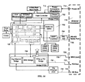
- FIG. 14 is a block diagram illustrating a single board computer 700 utilizing techniques according to the present subject matter.
- This present subject matter is embodied in, for example, the Proton400k computer made by Space Micro, Inc. of San Diego, Calif.
- the processor 100 is connected to an input circuit 702 and to an output circuit 704 .
- Each of input and output circuits 702 and 704 could comprise an RTAX2000SL Bridge FPGA, made by Micro semi SoC Products Group (formerly Actel) of Mountain View, Calif.
- a connector 710 connects the computer 700 to systems which use the computer 700 .
- a power converter 712 powering the computer 700 , receives power from connector power terminal 714 .
- the output circuit 704 exchanges data with the connector 710 at terminals 720 , 722 , and 724 respectively connected to buses 730 , 732 , and 734 .
- the buses 730 , 732 , and 734 are respectively a serial rapid I/O bus (SRIO), a PCI bus, and a Gigabit Ethernet Bus.
- Terminal 750 connects via an RS-422 bus to a universal asynchronous receiver/transmitter (UART) control circuit 754 .
- UART universal asynchronous receiver/transmitter
Abstract
Description
Claims (16)
Priority Applications (1)
| Application Number | Priority Date | Filing Date | Title |
|---|---|---|---|
| US12/928,084 US8886994B2 (en) | 2009-12-07 | 2010-12-03 | Radiation hard and fault tolerant multicore processor and method for ionizing radiation environment |
Applications Claiming Priority (2)
| Application Number | Priority Date | Filing Date | Title |
|---|---|---|---|
| US28349509P | 2009-12-07 | 2009-12-07 | |
| US12/928,084 US8886994B2 (en) | 2009-12-07 | 2010-12-03 | Radiation hard and fault tolerant multicore processor and method for ionizing radiation environment |
Publications (2)
| Publication Number | Publication Date |
|---|---|
| US20110208997A1 US20110208997A1 (en) | 2011-08-25 |
| US8886994B2 true US8886994B2 (en) | 2014-11-11 |
Family
ID=44477484
Family Applications (1)
| Application Number | Title | Priority Date | Filing Date |
|---|---|---|---|
| US12/928,084 Expired - Fee Related US8886994B2 (en) | 2009-12-07 | 2010-12-03 | Radiation hard and fault tolerant multicore processor and method for ionizing radiation environment |
Country Status (1)
| Country | Link |
|---|---|
| US (1) | US8886994B2 (en) |
Cited By (6)
| Publication number | Priority date | Publication date | Assignee | Title |
|---|---|---|---|---|
| CN107038095A (en) * | 2015-09-30 | 2017-08-11 | 罗伯特·博世有限公司 | method for redundantly processing data |
| RU2724804C1 (en) * | 2019-11-27 | 2020-06-25 | Федеральное государственное бюджетное учреждение "Национальный исследовательский центр "Курчатовский институт" | Method for indirect measurement of fail-safety of irradiated test digital microcircuits, which are built using different methods of permanent element-by-element redundancy, and functional structure of test microchip intended for implementation of this method |
| US10922203B1 (en) * | 2018-09-21 | 2021-02-16 | Nvidia Corporation | Fault injection architecture for resilient GPU computing |
| US11362678B2 (en) | 2011-12-30 | 2022-06-14 | Streamscale, Inc. | Accelerated erasure coding system and method |
| US11500723B2 (en) | 2011-12-30 | 2022-11-15 | Streamscale, Inc. | Using parity data for concurrent data authentication, correction, compression, and encryption |
| US11888418B2 (en) | 2021-02-12 | 2024-01-30 | Hamilton Sundstrand Corporation | Control structures for parallel motor drive control architectures |
Families Citing this family (18)
| Publication number | Priority date | Publication date | Assignee | Title |
|---|---|---|---|---|
| US8032889B2 (en) * | 2006-04-05 | 2011-10-04 | Maxwell Technologies, Inc. | Methods and apparatus for managing and controlling power consumption and heat generation in computer systems |
| EP2633408B1 (en) * | 2010-10-28 | 2018-08-22 | Data Device Corporation | System, method and apparatus for error correction in multi-processor systems |
| US10031888B2 (en) * | 2011-02-17 | 2018-07-24 | Hyperion Core, Inc. | Parallel memory systems |
| GB2495959A (en) * | 2011-10-26 | 2013-05-01 | Imagination Tech Ltd | Multi-threaded memory access processor |
| US9052911B2 (en) * | 2012-08-14 | 2015-06-09 | Oracle International Corporation | Mechanism for consistent core hang detection in a a processor core |
| US20150286544A1 (en) * | 2012-11-29 | 2015-10-08 | Hewlett-Packard Development Company, L.P. | Fault tolerance in a multi-core circuit |
| KR20140134376A (en) * | 2013-05-14 | 2014-11-24 | 한국전자통신연구원 | Processor capable of fault detection and method of detecting fault of processor core using the same |
| ES2696604T3 (en) * | 2013-12-13 | 2019-01-17 | Thales Sa | Fault tolerant framework architecture with triple software redundancy |
| FR3019667B1 (en) * | 2014-04-07 | 2018-03-09 | Zodiac Aero Electric | DATA PROCESSING SYSTEM FOR GRAPHICAL INTERFACE AND GRAPHICAL INTERFACE HAVING SUCH A DATA PROCESSING SYSTEM |
| CN106414214A (en) * | 2014-04-16 | 2017-02-15 | 西门子工业公司 | Railway safety critical systems with task redundancy and asymmetric communications capability |
| CN104391763B (en) * | 2014-12-17 | 2016-05-18 | 中国人民解放军国防科学技术大学 | Many-core processor fault-tolerance approach based on device view redundancy |
| CN104536350B (en) * | 2014-12-31 | 2017-04-12 | 浙江中控技术股份有限公司 | Work, standby and preemption type real-time multi-task controller and redundancy synchronous method thereof |
| JP2017151785A (en) * | 2016-02-25 | 2017-08-31 | ルネサスエレクトロニクス株式会社 | Semiconductor device |
| US10579536B2 (en) * | 2016-08-09 | 2020-03-03 | Arizona Board Of Regents On Behalf Of Arizona State University | Multi-mode radiation hardened multi-core microprocessors |
| CN106528401B (en) * | 2016-09-28 | 2019-10-11 | 北京广利核系统工程有限公司 | The tripping test method and device of control system based on redundancy structure |
| CN108052420B (en) * | 2018-01-08 | 2021-11-02 | 哈尔滨工业大学 | Zynq-7000-based dual-core ARM processor single event upset resistance protection method |
| CN109144793B (en) * | 2018-09-07 | 2021-12-31 | 合肥工业大学 | Fault correction device and method based on data flow driving calculation |
| JP6729825B1 (en) * | 2020-02-04 | 2020-07-22 | オムロン株式会社 | Information processing apparatus, control method, and program |
Citations (10)
| Publication number | Priority date | Publication date | Assignee | Title |
|---|---|---|---|---|
| US20030188222A1 (en) * | 2002-03-29 | 2003-10-02 | International Business Machines Corporation | Fail-over control in a computer system having redundant service processors |
| US20080082893A1 (en) | 2006-09-29 | 2008-04-03 | University Of Connecticut | Error-tolerant multi-threaded memory systems with reduced error accumulation |
| US20080091996A1 (en) * | 2006-09-28 | 2008-04-17 | Cisco Technology, Inc. | Single event upset test circuit and methodology |
| US20080189538A1 (en) * | 2007-02-06 | 2008-08-07 | Microsoft Corporation | Supporting multiple operating systems in media devices |
| US20080216074A1 (en) * | 2002-10-08 | 2008-09-04 | Hass David T | Advanced processor translation lookaside buffer management in a multithreaded system |
| US20090031317A1 (en) | 2007-07-24 | 2009-01-29 | Microsoft Corporation | Scheduling threads in multi-core systems |
| US20090044044A1 (en) * | 2005-11-18 | 2009-02-12 | Werner Harter | Device and method for correcting errors in a system having at least two execution units having registers |
| US20100037038A1 (en) * | 2008-08-06 | 2010-02-11 | International Business Machines Corporation | Dynamic Core Pool Management |
| US7734970B2 (en) | 2005-07-28 | 2010-06-08 | International Business Machines Corporation | Self-resetting, self-correcting latches |
| US20100318774A1 (en) * | 2009-06-12 | 2010-12-16 | Cray Inc. | Processor instruction graduation timeout |
-
2010
- 2010-12-03 US US12/928,084 patent/US8886994B2/en not_active Expired - Fee Related
Patent Citations (10)
| Publication number | Priority date | Publication date | Assignee | Title |
|---|---|---|---|---|
| US20030188222A1 (en) * | 2002-03-29 | 2003-10-02 | International Business Machines Corporation | Fail-over control in a computer system having redundant service processors |
| US20080216074A1 (en) * | 2002-10-08 | 2008-09-04 | Hass David T | Advanced processor translation lookaside buffer management in a multithreaded system |
| US7734970B2 (en) | 2005-07-28 | 2010-06-08 | International Business Machines Corporation | Self-resetting, self-correcting latches |
| US20090044044A1 (en) * | 2005-11-18 | 2009-02-12 | Werner Harter | Device and method for correcting errors in a system having at least two execution units having registers |
| US20080091996A1 (en) * | 2006-09-28 | 2008-04-17 | Cisco Technology, Inc. | Single event upset test circuit and methodology |
| US20080082893A1 (en) | 2006-09-29 | 2008-04-03 | University Of Connecticut | Error-tolerant multi-threaded memory systems with reduced error accumulation |
| US20080189538A1 (en) * | 2007-02-06 | 2008-08-07 | Microsoft Corporation | Supporting multiple operating systems in media devices |
| US20090031317A1 (en) | 2007-07-24 | 2009-01-29 | Microsoft Corporation | Scheduling threads in multi-core systems |
| US20100037038A1 (en) * | 2008-08-06 | 2010-02-11 | International Business Machines Corporation | Dynamic Core Pool Management |
| US20100318774A1 (en) * | 2009-06-12 | 2010-12-16 | Cray Inc. | Processor instruction graduation timeout |
Cited By (10)
| Publication number | Priority date | Publication date | Assignee | Title |
|---|---|---|---|---|
| US11362678B2 (en) | 2011-12-30 | 2022-06-14 | Streamscale, Inc. | Accelerated erasure coding system and method |
| US11500723B2 (en) | 2011-12-30 | 2022-11-15 | Streamscale, Inc. | Using parity data for concurrent data authentication, correction, compression, and encryption |
| US11736125B2 (en) | 2011-12-30 | 2023-08-22 | Streamscale, Inc. | Accelerated erasure coding system and method |
| CN107038095A (en) * | 2015-09-30 | 2017-08-11 | 罗伯特·博世有限公司 | method for redundantly processing data |
| CN107038095B (en) * | 2015-09-30 | 2021-09-24 | 罗伯特·博世有限公司 | Method for redundantly processing data |
| US10922203B1 (en) * | 2018-09-21 | 2021-02-16 | Nvidia Corporation | Fault injection architecture for resilient GPU computing |
| US20220156169A1 (en) * | 2018-09-21 | 2022-05-19 | Nvidia Corporation | Fault injection architecture for resilient gpu computing |
| US11669421B2 (en) * | 2018-09-21 | 2023-06-06 | Nvidia Corporation | Fault injection architecture for resilient GPU computing |
| RU2724804C1 (en) * | 2019-11-27 | 2020-06-25 | Федеральное государственное бюджетное учреждение "Национальный исследовательский центр "Курчатовский институт" | Method for indirect measurement of fail-safety of irradiated test digital microcircuits, which are built using different methods of permanent element-by-element redundancy, and functional structure of test microchip intended for implementation of this method |
| US11888418B2 (en) | 2021-02-12 | 2024-01-30 | Hamilton Sundstrand Corporation | Control structures for parallel motor drive control architectures |
Also Published As
| Publication number | Publication date |
|---|---|
| US20110208997A1 (en) | 2011-08-25 |
Similar Documents
| Publication | Publication Date | Title |
|---|---|---|
| US8886994B2 (en) | Radiation hard and fault tolerant multicore processor and method for ionizing radiation environment | |
| Iturbe et al. | A triple core lock-step (tcls) arm® cortex®-r5 processor for safety-critical and ultra-reliable applications | |
| US8930752B2 (en) | Scheduler for multiprocessor system switch with selective pairing | |
| US9823983B2 (en) | Electronic fault detection unit | |
| US10095601B2 (en) | Triple software redundancy fault tolerant framework architecture | |
| US5903717A (en) | Fault tolerant computer system | |
| US8635492B2 (en) | State recovery and lockstep execution restart in a system with multiprocessor pairing | |
| US8671311B2 (en) | Multiprocessor switch with selective pairing | |
| US6938183B2 (en) | Fault tolerant processing architecture | |
| US7260742B2 (en) | SEU and SEFI fault tolerant computer | |
| US6393582B1 (en) | Error self-checking and recovery using lock-step processor pair architecture | |
| EP3493062A2 (en) | Data processing system having lockstep operation | |
| US10078565B1 (en) | Error recovery for redundant processing circuits | |
| US20040216003A1 (en) | Mechanism for FRU fault isolation in distributed nodal environment | |
| JPH0683663A (en) | Multiprocessor computer system | |
| Missimer et al. | Distributed real-time fault tolerance on a virtualized multi-core system | |
| EP1146423B1 (en) | Voted processing system | |
| US20060184840A1 (en) | Using timebase register for system checkstop in clock running environment in a distributed nodal environment | |
| US20040193735A1 (en) | Method and circuit arrangement for synchronization of synchronously or asynchronously clocked processor units | |
| CN108052420B (en) | Zynq-7000-based dual-core ARM processor single event upset resistance protection method | |
| Liu et al. | A survey of fault tolerance hardware architecture | |
| Szurman et al. | Coarse-Grained TMR Soft-Core Processor Fault Tolerance Methods and State Synchronization for Run-Time Fault Recovery | |
| WALTER | MAFT-An architecture for reliable fly-by-wire flight control | |
| Shen et al. | Microkernel mechanisms for improving the trustworthiness of commodity hardware | |
| EP4332809A1 (en) | End-to-end transaction integrity through standard interconnect |
Legal Events
| Date | Code | Title | Description |
|---|---|---|---|
| AS | Assignment |
Owner name: SPACE MICRO, INC., CALIFORNIA Free format text: ASSIGNMENT OF ASSIGNORS INTEREST;ASSIGNOR:CZAJKOWSKI, DAVID R.;REEL/FRAME:025485/0858 Effective date: 20101203 |
|
| AS | Assignment |
Owner name: FUJITSU LIMITED, JAPAN Free format text: ASSIGNMENT OF ASSIGNORS INTEREST;ASSIGNORS:WADA, YUJI;KATSUNO, AKIRA;MATSUMOTO, YASUHIDE;AND OTHERS;SIGNING DATES FROM 20101108 TO 20101112;REEL/FRAME:025633/0774 |
|
| AS | Assignment |
Owner name: FUJITSU LIMITED, JAPAN Free format text: ASSIGNMENT OF ASSIGNORS INTEREST;ASSIGNORS:WADA, YUJI;KATSUNO, AKIRA;MATSUMOTO, YASUHIDE;AND OTHERS;SIGNING DATES FROM 20101108 TO 20101112;REEL/FRAME:026517/0798 |
|
| STCF | Information on status: patent grant |
Free format text: PATENTED CASE |
|
| FEPP | Fee payment procedure |
Free format text: MAINTENANCE FEE REMINDER MAILED (ORIGINAL EVENT CODE: REM.) |
|
| FEPP | Fee payment procedure |
Free format text: SURCHARGE FOR LATE PAYMENT, SMALL ENTITY (ORIGINAL EVENT CODE: M2554) |
|
| MAFP | Maintenance fee payment |
Free format text: PAYMENT OF MAINTENANCE FEE, 4TH YR, SMALL ENTITY (ORIGINAL EVENT CODE: M2551) Year of fee payment: 4 |
|
| FEPP | Fee payment procedure |
Free format text: MAINTENANCE FEE REMINDER MAILED (ORIGINAL EVENT CODE: REM.); ENTITY STATUS OF PATENT OWNER: SMALL ENTITY |
|
| LAPS | Lapse for failure to pay maintenance fees |
Free format text: PATENT EXPIRED FOR FAILURE TO PAY MAINTENANCE FEES (ORIGINAL EVENT CODE: EXP.); ENTITY STATUS OF PATENT OWNER: SMALL ENTITY |
|
| STCH | Information on status: patent discontinuation |
Free format text: PATENT EXPIRED DUE TO NONPAYMENT OF MAINTENANCE FEES UNDER 37 CFR 1.362 |
|
| FP | Lapsed due to failure to pay maintenance fee |
Effective date: 20221111 |