US8884517B1 - Illumination sources with thermally-isolated electronics - Google Patents
Illumination sources with thermally-isolated electronics Download PDFInfo
- Publication number
- US8884517B1 US8884517B1 US13/274,489 US201113274489A US8884517B1 US 8884517 B1 US8884517 B1 US 8884517B1 US 201113274489 A US201113274489 A US 201113274489A US 8884517 B1 US8884517 B1 US 8884517B1
- Authority
- US
- United States
- Prior art keywords
- heat dissipation
- heat
- dissipation portion
- illumination source
- led
- Prior art date
- Legal status (The legal status is an assumption and is not a legal conclusion. Google has not performed a legal analysis and makes no representation as to the accuracy of the status listed.)
- Active, expires
Links
Images


Classifications
-
- F—MECHANICAL ENGINEERING; LIGHTING; HEATING; WEAPONS; BLASTING
- F21—LIGHTING
- F21V—FUNCTIONAL FEATURES OR DETAILS OF LIGHTING DEVICES OR SYSTEMS THEREOF; STRUCTURAL COMBINATIONS OF LIGHTING DEVICES WITH OTHER ARTICLES, NOT OTHERWISE PROVIDED FOR
- F21V29/00—Protecting lighting devices from thermal damage; Cooling or heating arrangements specially adapted for lighting devices or systems
- F21V29/15—Thermal insulation
-
- F—MECHANICAL ENGINEERING; LIGHTING; HEATING; WEAPONS; BLASTING
- F21—LIGHTING
- F21K—NON-ELECTRIC LIGHT SOURCES USING LUMINESCENCE; LIGHT SOURCES USING ELECTROCHEMILUMINESCENCE; LIGHT SOURCES USING CHARGES OF COMBUSTIBLE MATERIAL; LIGHT SOURCES USING SEMICONDUCTOR DEVICES AS LIGHT-GENERATING ELEMENTS; LIGHT SOURCES NOT OTHERWISE PROVIDED FOR
- F21K9/00—Light sources using semiconductor devices as light-generating elements, e.g. using light-emitting diodes [LED] or lasers
- F21K9/20—Light sources comprising attachment means
- F21K9/23—Retrofit light sources for lighting devices with a single fitting for each light source, e.g. for substitution of incandescent lamps with bayonet or threaded fittings
-
- F—MECHANICAL ENGINEERING; LIGHTING; HEATING; WEAPONS; BLASTING
- F21—LIGHTING
- F21K—NON-ELECTRIC LIGHT SOURCES USING LUMINESCENCE; LIGHT SOURCES USING ELECTROCHEMILUMINESCENCE; LIGHT SOURCES USING CHARGES OF COMBUSTIBLE MATERIAL; LIGHT SOURCES USING SEMICONDUCTOR DEVICES AS LIGHT-GENERATING ELEMENTS; LIGHT SOURCES NOT OTHERWISE PROVIDED FOR
- F21K9/00—Light sources using semiconductor devices as light-generating elements, e.g. using light-emitting diodes [LED] or lasers
- F21K9/90—Methods of manufacture
-
- F—MECHANICAL ENGINEERING; LIGHTING; HEATING; WEAPONS; BLASTING
- F21—LIGHTING
- F21V—FUNCTIONAL FEATURES OR DETAILS OF LIGHTING DEVICES OR SYSTEMS THEREOF; STRUCTURAL COMBINATIONS OF LIGHTING DEVICES WITH OTHER ARTICLES, NOT OTHERWISE PROVIDED FOR
- F21V29/00—Protecting lighting devices from thermal damage; Cooling or heating arrangements specially adapted for lighting devices or systems
- F21V29/50—Cooling arrangements
- F21V29/70—Cooling arrangements characterised by passive heat-dissipating elements, e.g. heat-sinks
- F21V29/83—Cooling arrangements characterised by passive heat-dissipating elements, e.g. heat-sinks the elements having apertures, ducts or channels, e.g. heat radiation holes
-
- F—MECHANICAL ENGINEERING; LIGHTING; HEATING; WEAPONS; BLASTING
- F21—LIGHTING
- F21V—FUNCTIONAL FEATURES OR DETAILS OF LIGHTING DEVICES OR SYSTEMS THEREOF; STRUCTURAL COMBINATIONS OF LIGHTING DEVICES WITH OTHER ARTICLES, NOT OTHERWISE PROVIDED FOR
- F21V29/00—Protecting lighting devices from thermal damage; Cooling or heating arrangements specially adapted for lighting devices or systems
- F21V29/50—Cooling arrangements
- F21V29/70—Cooling arrangements characterised by passive heat-dissipating elements, e.g. heat-sinks
- F21V29/74—Cooling arrangements characterised by passive heat-dissipating elements, e.g. heat-sinks with fins or blades
-
- F—MECHANICAL ENGINEERING; LIGHTING; HEATING; WEAPONS; BLASTING
- F21—LIGHTING
- F21Y—INDEXING SCHEME ASSOCIATED WITH SUBCLASSES F21K, F21L, F21S and F21V, RELATING TO THE FORM OR THE KIND OF THE LIGHT SOURCES OR OF THE COLOUR OF THE LIGHT EMITTED
- F21Y2105/00—Planar light sources
- F21Y2105/10—Planar light sources comprising a two-dimensional array of point-like light-generating elements
-
- F—MECHANICAL ENGINEERING; LIGHTING; HEATING; WEAPONS; BLASTING
- F21—LIGHTING
- F21Y—INDEXING SCHEME ASSOCIATED WITH SUBCLASSES F21K, F21L, F21S and F21V, RELATING TO THE FORM OR THE KIND OF THE LIGHT SOURCES OR OF THE COLOUR OF THE LIGHT EMITTED
- F21Y2115/00—Light-generating elements of semiconductor light sources
- F21Y2115/10—Light-emitting diodes [LED]
Definitions
- the present invention relates to lighting. More specifically, the present invention relates to high efficiency lighting sources.
- fluorescent lighting sources typically rely upon mercury in a vapor form to produce light. Because the mercury vapor is considered a hazardous material, spent lamps cannot simply be disposed of at the curbside but must be transported to designated hazardous waste disposal sites. Additionally, some fluorescent tube manufacturers go so far as to instruct the consumer to avoid using the bulb in more sensitive areas of the house such as bedrooms, kitchens, and the like.
- fluorescent lighting sources often rely upon a separate starter or ballast mechanism to initiate the illumination. Because of this, fluorescent lights sometimes do not turn on “instantaneously” as consumers expect and demand. Further, fluorescent lights typically do not immediately provide light at full brightness, but typically ramp up to full brightness within an amount of time (e.g. 30 seconds). Further, most fluorescent lights are fragile, are not capable of dimming, have ballast transformers that can emit annoying audible noise, and can fail in a shortened period of time if cycled on and off frequently. Because of this, fluorescent lights do not have the performance consumers require.
- LEDs light emitting diodes
- LEDs have advantages over fluorescent lights including the robustness and reliability inherent in solid state devices, the lack of toxic chemicals that can be released during accidental breakage or disposal, instant-on capabilities, dimmability, and the lack of audible noise.
- the inventors of the present invention believe, however, that current LED lighting sources themselves have significant drawbacks that cause consumers to be reluctant to using them.
- a key drawback with current LED lighting sources is that the light output (e.g. lumens) is relatively low.
- current LED lighting sources draw a significantly lower amount of power than their incandescent equivalents (e.g. 5-10 watts v. 50 watts), they are believe to be far too dim to be used as primary lighting sources.
- a typical 5 watt LED lamp in the MR16 form factor may provide 200-300 lumens
- a typical 50 watt incandescent bulb in the same form factor may provide 700-1000 lumens.
- current LEDs are often used only for exterior accent lighting, closets, basements, sheds or other small spaces.
- LED lighting sources Another drawback with current LED lighting sources includes that the upfront cost of the LED is often shockingly high to consumers. For example, for floodlights, a current 30 watt equivalent LED bulb may retail for over $60, whereas a typical incandescent floodlight may retail for $12. Although the consumer may rationally “make up the difference” over the lifetime of the LED by the LED consuming less power, the inventors believe the significantly higher prices greatly suppress consumer demand. Because of this, current LED lighting sources do not have the price or performance that consumers expect and demand.
- Additional drawbacks with current LED lighting sources includes they have many parts and are labor intensive to produce. As merely an example, one manufacturer of an MR16 LED lighting source utilizes over 14 components (excluding electronic chips), and another manufacturer of an MR 16 LED lighting source utilizes over 60 components. The inventors of the present invention believe that these manufacturing and testing processes are more complicated and more time consuming, compared to manufacturing and testing of a LED device with fewer parts and a more modular manufacturing process.
- LED lighting sources have been increased by simply increasing the number of LEDs, which has lead to increased device costs, and increased device size. Additionally, such lights have had limited beam angles and limited outputs.
- This invention relates to high efficient lighting sources. More specifically, the invention relates to a LED lighting source and methods of manufacturing thereof. Some general goals include, to increase light output without increasing device cost or device size, to enable coverage of many beam angles, and to provide a high reliability product for long life (ROI).
- ROI long life
- Embodiments of the invention include a modular lighting source. More specifically, various embodiments include an MR16 form factor light source.
- a lighting module includes from 20 to 110 LEDs arrayed in series upon a thermally conductive substrate (e.g. silicon substrate). The silicon substrate is soldered to a flexible printed circuit substrate (FPC) having a pair of input power connectors on a first surface. The silicon substrate is physically bonded to an MR16 form factor heat sink via a thermal epoxy on a second surface.
- a driving module includes a high-temperature operating driving circuit soldered to a rigid printed circuit board or a flexible printed circuit substrate. The driving circuit and FPC are encased in a thermally conductive plug base that is compatible with an MR16 plug, forming the base assembly module.
- a potting compound facilitating heat transfer from the driving circuit to the thermally conductive plug case is typically used.
- the driving circuits are coupled to input power contacts (e.g. 12, 24, 120, 220 volt AC) and coupled to output power connectors (e.g. 40 VAC, 120 VAC, etc.)
- the base assembly module is inserted into and secured within an interior channel of the MR16 form factor heat sink.
- the input power connectors are coupled to the output power connectors.
- a lens is then secured to the heat sink.
- the driving module transforms the input power from 12 AC volts to a higher DC voltage, such as 40 volts to 120 Volts.
- the driving module drives the lighting module with the higher voltage, and the lighting module emits the light.
- the light is conditioned with the lens to the desired type of lighting, e.g. spot, flood, etc.
- the driving module and the lighting module produce heat that is dissipated by the MR16 form factor heat sink. At steady state, these modules usually operate in the range of approximately 75° C. to 130° C.
- the MR16 form factor heat sink facilitates the dissipation of heat.
- the heat sink includes an inner core that has a diameter less than half the outer diameter of the heat sink. In various embodiments, the inner core is less than one third, one fourth, and one fifth the outer diameter.
- the silicon substrate of the LEDs is directly bonded to the inner core region via the thermal epoxy.
- Typical fin configurations include a number radiating fin “trunks” extending from the inner core. In some embodiments, the number of trunks range from 8 to 35. At the end of each trunk, two or more fin “branches” are provided having “U” branching shape. In various embodiments, at the end of each branch, two or more fin “sub-branches” are provided, also having a “U” branching shape.
- the fin thickness of the trunk may be thicker than the branches, which in turn may be thicker than the sub-branches, etc.
- the amount of heat flow from the inner core towards the outer diameter, airflow, and surface area are therefore engineered to increase heat dissipating capability.
- an illumination source configured to provide electrical power output in response to external electrical power input, wherein the electronic power portion generates heat in response to the external electrical power input, and a light producing portion coupled to the electronic driving portion, wherein the light generating portion is configured to output light energy in response to the electrical power output, wherein the light producing portion generates heat in response to the electrical power output.
- An apparatus includes a first heat dissipation portion physically coupled to the electronic power portion, wherein the first heat dissipation portion is configured to receive the heat from the electronic power portion and configured to dissipate the heat from the electronic power portion, and a second heat dissipation portion physically coupled to the light producing portion, wherein the second heat dissipation portion is configured to receive heat from the light producing portion and configured to dissipate the heat from the light producing portion.
- a system includes an insulating portion physically disposed between the first heat dissipation portion and the second heat dissipation portion, wherein the insulator portion is configured to inhibit the heat from the light producing portion from being transferred to the electronic power portion.
- a method for assembling an illumination source includes providing an electronic power portion configured to provide electrical power output in response to external electrical power input, wherein the electronic power portion generates heat in response to the external electrical power input, providing a first heat dissipation portion, wherein the first heat dissipation portion is configured to receive the heat from the electronic power portion and configured to dissipate the heat from the electronic power portion, and physically coupling the electronic power portion to the first heat dissipation portion to form a driving portion.
- One process includes providing a light producing portion, wherein the light generating portion is configured to output light energy in response to the electrical power output, wherein the light producing portion generates heat in response to the electrical power output, providing a second heat dissipation portion, wherein the second heat dissipation portion is configured to receive heat from the light producing portion and configured to dissipate the heat from the light producing portion, and physically coupling the light producing portion to the second heat dissipation portion to form a lighting portion.
- a method includes providing an insulating portion, and physically coupling the driving portion to the lighting portion via the insulating portion, wherein the insulator portion is configured to inhibit the heat from the lighting portion from being transferred to the driving portion.
- aspects of various embodiments include: simplified construction facilitating high volume manufacturing, flex interconnects to eliminate hand wiring, modular subassembly construction to enable parallel processing.
- Other features include thermal management aspects: fin branching algorithm, reduced cross section central core, airflow behind lens, single thermal interface, direct die attach, flex printed circuits in base, base contour to minimize potting material, recessed front, ensured airflow with coverage; low-cost manufacturing: flexible printed circuit interconnect (main and interposer), separable driver module, flex circuit light chip interposer, redundant latching and bonding features, and the like.
- aspects include: high temperature operation enabling a densely packed LED array, higher component reliability, high heat dissipation, maximum surface area, maximum airflow, minimum thermal interface losses, minimum length thermal paths within the electronics module, and the like.
- Advantage with embodiments of the present invention include operating a LED light source reliably at high temperatures, allowing the concentration of a large number of LEDs in a small space while simultaneously operating them at higher power levels.
- FIGS. 1A-B illustrate various embodiments of the present invention
- FIGS. 2A-B illustrates modular diagrams according to various embodiments of the present invention
- FIGS. 3A-B illustrate an embodiment of the present invention
- FIGS. 4A-C illustrate various embodiments of the present invention
- FIGS. 5A-B illustrate various embodiments of the present invention
- FIGS. 6A-B illustrate various embodiments of the present invention
- FIGS. 7A-C illustrate a block diagram of a manufacturing process according to embodiments of the present invention.
- FIGS. 8A-B illustrate various embodiments of the present invention.
- FIG. 9 illustrates various embodiments of the present invention.
- FIGS. 1A-B illustrate various embodiments of the present invention. More specifically, FIGS. 1A-B illustrate embodiments of MR-16 form factor compatible LED lighting sources 100 and 110 having GU 5.3 form factor compatible bases 120 and 130 . Such MR-16 lighting sources typically operate upon 12 volts, alternating current (e.g. VAC). In the examples illustrated, LED lighting source 100 is configured to provide a spot light having a 10 degree beam size and LED lighting source 110 is configured to provide a flood light having a 25 or 40 degree beam size.
- alternating current e.g. VAC
- LED lighting source 100 may provide a peak output brightness from approximately 7600 to 8600 candelas (with approximately 360 to 400 lumens)
- LED lighting source 110 may provide a peak output brightness of approximately 1050 to 1400 candelas for a 40 degree flood light (with approximately 510 to 650 lumens)
- approximately 2300 to 2500 candelas for a 25 degree flood light with approximately 620 to 670 lumens.
- Various embodiments of the present invention therefore are believed to have achieve the same brightness as conventional halogen bulb MR-16 lights.
- FIGS. 2A-B illustrates modular diagrams according to various embodiments of the present invention. More specifically, FIG. 2A illustrates a modular diagram of a spot light 200 , and FIG. 2B illustrates a modular diagram of a flood light 250 .
- spotlight 200 includes a lens 210 , an LED assembly/module 220 , a heat sink 230 , and a base assembly/module 240 .
- flood light 250 includes a lens 260 , a lens holder 270 , an LED assembly/module 280 , a heat sink 290 , and a base assembly/module 295 .
- the modular approach to assembling spotlight 200 or floodlight 250 are believed to reduce the manufacturing complexity, reduce manufacturing costs, and increase the reliability of such lights.
- Lens 210 and/or lens 260 may be formed from a UV and resistant transparent material, such as glass, polycarbonate material, or the like. Lens 210 and 26 also may be solid. In the case of lens 210 , the solid material creates a folded light path such that light that is generated by the LED assembly 220 internally reflects within lens 210 more than one time prior to being output. Such a folded optic lens enables spotlight 200 to have a tighter columniation of light than is normally available from a conventional reflector of equivalent depth.
- the transparent material should be operable at an elevated temperature (e.g. 120 degrees C.) for a prolonged period of time (e.g. hours).
- elevated temperature e.g. 120 degrees C.
- One material that may be used for lens 210 and/or lens 260 is known as MakrolonTM LED 2045 or LED 2245 polycarbonate available from Bayer Material Science AG. In other embodiments, other similar materials may also be used.
- lens 210 is secured to heat sink 230 via one or more clips integrally formed on the edge of lens 210 .
- lens 210 may also be secured via an adhesive proximate to where LED assembly 220 is secured to heat sink 230 .
- lens 260 may be secured to a lens holder 270 via one or more tabs integrally formed on the edge of lens 260 .
- lens holder 270 may be secured to heat sink 290 by one or more tabs integrally formed on the edge of lens holder 270 , as illustrated.
- lens holder 270 may be formed of plastic material that is preferably white colored to reflect backward scattered light back through the lens. Other similar heat resistant materials may also be used for lens holder 270 .
- the LED assembly 220 and LED assembly 280 may be of similar construction, and thus interchangeable during the manufacturing process.
- LED assemblies may be binned based upon lumen per watt efficacy. For example, in some examples, a LED assembly having a lumen per watt (L/W) efficacy from 53 to 66 L/W may be binned for use for 40 degree flood lights, a LED assembly having an efficacy of approximately 60 L/W may be binned for use for spot lights, a LED assembly having an efficacy of approximately 63 to 67 L/W may be use for 25 degree flood lights, and the like. In other embodiments, other classification or categorization of LED assemblies on the basis of L/W efficacy may used for other target applications.
- LED assembly 220 and LED assembly 280 typically include 36 LEDs arranged in series, in parallel series (e.g. three parallel strings of 12 LEDs in series), or the like. Further detail regarding such LED assemblies are provided in the patent applications incorporated by reference above.
- the targeted power consumption for LED assemblies is less than 13 watts. This is much less than the typical power consumption of halogen based MR16 lights (50 watts). Accordingly, embodiments of the present invention are able to match the brightness or intensity of halogen based MR16 lights, but using less than 20% of the energy.
- LED assembly 220 is directly secured to heat sink 230 and LED assembly 280 is directly secured to heat sink 280 .
- LED assemblies 220 and 280 typically includes a flat substrate such as silicon or the like. In various embodiments, it is contemplated that an operating temperature of LED assemblies 220 and 280 may be on the order of 125 to 140 degrees C.
- the silicon substrate is then secured to the heat sink using a high thermal conductivity epoxy (e.g. thermal conductivity ⁇ 96 W/m ⁇ k.).
- a thermoplastic/thermo set epoxy may be used such as TS-369, TS-3332-LD, or the like, available from Tanaka Kikinzoku Kogyo K.K. Other epoxies may also be used.
- no screws are otherwise used to secure the LED assembly to the heat sink, however, screws or other fastening means may also be used in other embodiments.
- Heat sinks 230 and 290 may be formed from a material having a low thermal resistance/high thermal conductivity.
- heat sink 290 has been measured to have a thermal resistance of approximately 7.5 degrees C./Watt.
- thermal resistance of as little as 6.6 degrees C./Watt are achievable in other embodiments.
- one of ordinary skill in the art will be able to envision other materials having different properties within embodiments of the present invention.
- base assemblies/modules 240 and 295 in FIGS. 2A-B provide a standard GU 5.3 physical and electronic interface to a light socket.
- base modules 240 and 295 includes high temperature resistant electronic circuitry used to drive LED modules 220 and 280 .
- an input voltage of 12 VAC to the lamps is converted to 120 VAC, 40 VAC, or other voltage by the LED driving circuitry.
- the driving voltage may be set depending upon specific LED configuration (e.g. series, parallel/series, etc.) desired.
- the shell of base assemblies 240 and 295 are typically formed from an aluminum alloy, and may formed from an alloy similar to that used for heat sink 230 and/or heat sink 290 .
- an alloy such as AL 1100 may be used.
- a compliant potting compound such as Omegabond® 200 available from Omega Engineering, Inc. or 50-1225 from Epoxies, Etc. may be used. In other embodiments, other types of heat transfer materials may be used.
- a thermally insulating material, sleeve, compound, or the like may be disposed between surfaces 245 and 285 of the base assemblies 240 and 295 and interior cavities of heat sinks 230 and 290 , respectively.
- the thermally insulating materials are provided to facilitate thermal isolation between base assemblies 240 and 295 from heat sinks 230 and 290 , respectively. More specifically, the thermally barrier functions to keep a steady-state operating temperature of base assemblies 240 and 295 lower than a steady-state operating temperature of heat sinks 230 and 290 , respectively.
- the operating temperature of heat sink 230 or 290 may be on the order of 120 C, near LED modules 220 or 280 , whereas the operating temperature of base assembly 240 or 295 may be on the order of 110 C, and less.
- the temperature difference may be on the order of 5 C or higher, 20 C or higher, or the like.
- One such benefit is that because the electronic circuits within the base assembly may be subject to a lower temperature, lower cost electronic components (with lower temperature ratings) may be used.
- Another benefit is that the reliability of such a lamp may be increased because the electronic circuits are subject to lower temperatures and will tend to have longer life spans.
- Yet another benefit is that such a lamp may be safer to use because less excess heat would be radiated to a lamp housing from the base assembly, compared to lamps without such an insulating layer.
- a thermally insulating material, sleeve, compound, or the like may be made of silicone, rubber, plastics, ceramic, and the like.
- the thermal barrier may be a solid object, as illustrated in FIG. 8B , and in other embodiments, the thermal barrier may be a paste-like compound.
- it is desired that a thermal conductivity is less than 2 watts/M*K, less than 1 watt/M*K, or the like.
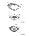
- FIGS. 3A-B illustrate an embodiment of the present invention. More specifically, FIG. 3A illustrates an LED package subassembly (LED module) according to various embodiments. More specifically, a plurality of LEDs 300 are illustrated disposed upon a substrate 310 . In some embodiments, it is contemplated that the plurality of LEDs 300 are connected in series and powered by a voltage source of approximately 120 volts AC (VAC). To enable a sufficient voltage drop (e.g. 3 to 4 volts) across each LED 300 , in various embodiments 30 to 40 LEDs are contemplated to be used. In specific embodiments, 37 to 39 LEDs are coupled in series. In other embodiments, LEDs 300 are connected in parallel series and powered by a voltage source of approximately 40 VAC.
- VAC 120 volts AC
- the plurality of LEDs 300 include 36 LEDs arranged in three groups each having 12 LEDs 300 coupled in series. Each group is thus coupled in parallel to the voltage source (40 VAC) provided by the LED driver circuitry, such that a sufficient voltage drop (e.g. 3 to 4 volts) is achieved across each LED 300 .
- a sufficient voltage drop e.g. 3 to 4 volts
- other driving voltages are envisioned, and other arrangements of LEDs 300 are also envisioned.
- the LEDs 300 are mounted upon a silicon substrate 310 , or other thermally conductive substrate.
- a thin electrically insulating layer and/or a reflective layer may separate LEDs 300 and the silicon substrate 310 .
- Heat produced from LEDs 300 is typically transferred to silicon substrate 310 and to a heat sink via a thermally conductive epoxy, as discussed above.
- the silicon substrate is approximately 5.7 mm ⁇ 5.7 mm in size, and approximately 0.6 microns in depth.
- the dimensions may vary according to specific lighting requirement. For example, for lower brightness intensity, fewer LEDs may be mounted upon the substrate, accordingly the substrate may decrease in size. In other embodiments, other substrate materials may be used and other shapes and sizes may also be used.
- a ring of silicone 315 is disposed around LEDs 300 to define a well-type structure.
- a phosphorus bearing material is disposed within the well structure.
- LEDs 300 provide a blue-ish light output, a violet, or a UV light output.
- the phosphorous bearing material is excited by the blue/uv output light, and emits white light output. Further details of embodiments of plurality of LEDs 300 and substrate 310 are described in the co-pending application incorporated by reference and referred to above.
- a number of bond pads 320 may be provided upon substrate 310 (e.g. 2 to 4). Then, a conventional solder layer (e.g. 96.5% tin and 5.5% gold) may be disposed upon silicon substrate 310 , such that one or more solder balls 330 are formed thereon.
- a conventional solder layer e.g. 96.5% tin and 5.5% gold
- four bond pads 320 are provided, one at each corner, two for each power supply connection. In other embodiments, only two bond pads may be used, one for each AC power supply connection.
- FPC 340 may include a flexible substrate material such as a polyimide, such as KaptonTM from DuPont, or the like. As illustrated, FPC 340 may have a series of bonding pads 350 , for bonding to silicon substrate 310 , and bonding pads 360 , for coupling to the high supply voltage (e.g. 120 VAC, 40 VAC, etc). Additionally, in some embodiments, an opening 370 is provided, through which LEDs 300 will shine through.
- the high supply voltage e.g. 120 VAC, 40 VAC, etc.
- an opening 370 is provided, through which LEDs 300 will shine through.
- FPC 340 Various shapes and sizes for FPC 340 are contemplated in various embodiments of the invention. For example, as illustrated in FIG. 3A , a series of cuts 380 may be made upon FPC 340 to reduce the effects of expansion and contraction of FPC 340 versus substrate 310 . As another example, a different number of bonding pads 350 may be provided, such as two bonding pads. As merely another example, FPC 340 may be crescent shaped, and opening 370 may not be a through hole. In other embodiments, other shapes and sizes for FPC 340 are contemplated in light of the present patent disclosure.
- substrate 310 is bonded to FPC 340 via solder balls 330 , in a conventional flip-chip type arrangement to the top surface of the silicon.
- solder balls 330 By making the electrical connection at the top surface of the silicon, it is electrically isolated from the heat transfer surface of the silicon. This allows the entire bottom surface of the silicon to transfer heat to the heat sink. Additionally, this allows the LED to bonded directly to the heat sink to maximize heat transfer instead of a PCB material that typically inhibits heat transfer.
- LEDs 300 are thus positioned to emit light through opening 370 .
- a under fill operation is performed using a silicone compound, or the like to seal the space 380 between substrate 310 and FPC 340 .
- the LED package sub assembly or module is thus assembled. In various embodiments, these LED modules may then be individually tested for proper operation.
- the LED sub assembly/module is thus assembled.
- these LED modules may then be individually tested for proper operation.
- FIGS. 4A-B illustrate various embodiments of the present invention. More specifically, FIGS. 4A-B illustrate embodiments of a driver module according to various embodiments.
- FIG. 4A illustrates embodiments of an LED driver circuit 400 for driving the LED module described above in FIGS. 3A-B .
- driver circuit 400 includes contacts 420 , and a flexible printed circuit (FPC) 430 electrically coupled to circuit board 410 .
- FPC 430 may be formed using a polyimide, such as KaptonTM as mentioned above.
- contacts 420 are conventional GU 5.3 compatible electrical contacts and provide driver circuit 400 an operating voltage (e.g. 12 VAC). In other embodiments, other base form factors for the electrical contacts, and other operating voltages are contemplated.
- Electrical components 440 may be disposed upon circuit board 410 and/or upon FPC 430 .
- the electrical components 440 includes circuitry that receives the operating voltage (e.g. 12 VAC) and converts it to an LED driving voltage (e.g. 40 VAC, 120 VAC, 180 VAC or the like).
- FIG. 4C illustrates an example circuit diagram providing this step-up voltage functionality.
- components 440 include a Max 16814 LED driving circuit available from Maxim Integrated Products, Inc. In other examples, other driving circuitry may also be used.
- the output LED driving voltage is provided upon bonding pads (e.g. contacts) 450 of FPC 430 .
- contacts 450 are coupled to bonding pads 360 of the LED module illustrated in FIGS. 3A-B , above.
- FIG. 4A illustrates various embodiments of a base casing.
- a base casing includes two separate portions 470 and 475 molded from an aluminum alloy.
- the shape of the base casing is to be mated into an MR-16 format compatible heat sink. More specifically, the base casing is inserted into and fastened within an interior channel of the heat sink. This may be seen in a subsequent drawing.
- LED driver circuit 400 is disposed between portions 470 and 475 , and contacts 420 and contacts 450 remain outside. Portions 470 and 475 may be welded together, glued together or otherwise secured. In various embodiments, portions 470 and 475 may include one or more molded protrusions that extend towards LED circuitry 440 , and may also be made of an aluminum alloy. The protrusions may be a series of pins, fins, or the like. Such protrusions may be provided as a way for heat to be conducted away from LED driver circuit 400 and towards the base casing. In various embodiments, the aluminum alloy is AL 1100, although other types and grades of aluminum may also be used, such as the aluminum alloy used for the heat sink.
- LED driving circuits at elevated temperatures for an MR-16 form factor light source has not been contemplated.
- electrical components 440 will be forced to operate at a high operating temperature, e.g. as high as 120° C., within the base casing.
- the source of the heat may include heat produced by electrical components 440 , themselves, as well as heat generated by the LED module. In the latter case, the LED module would transfer heat to the base casing via the heat sink.
- components of LED electrical circuitry 440 are selected for operation at these elevated temperatures (e.g. MILSPEC components).
- a potting compound such as a thermally conductive silicone rubber (Epoxies.com 50-1225, Omegabond® available from Omega Engineering, Inc., or the like) may be injected or disposed within the interior of the base casing.
- the potting compound is placed into physical contact with LED driver circuits 400 and the base casing, and it helps conduct heat generated by LED driver circuitry 400 outwards to the base casing.
- the generated heat may be dissipated via the base casing and/or the heat sink.
- the base sub assembly/module is thus assembled.
- these base modules may then be individually tested for proper operation.
- FIGS. 5A-B illustrate various embodiment of the present invention. More specifically, FIG. 5A-B illustrates various views of an embodiment of a heat sink 500 for an MR-16 compatible spot light.
- heat sink 500 and 510 are composed of an aluminum alloy that is thermally conductive, i.e. has low thermal resistance.
- heat sinks 500 and 510 may be formed from a material having a low thermal resistance/high thermal conductivity.
- a relatively flat section 520 helps define an inner core region 530 , and an outer core region 540 .
- the brightness of the LED modules can match the brightness of conventional 50 watt halogen MR-16 lights, but only consume 20% of the power. As illustrated above, the LED modules can provide this brightness in a small form factor.
- a LED module described above is bonded to flat section 520 of inner core 530 , and outer core 540 helps dissipate the heat generated by the light module and by the base module. As described above, in some embodiments, no screws or other fasteners are used to secure the LED module to flat section 520 . In some cases a thermal energy transferring epoxy, or the like may be used.
- the inner core region 530 the light generating region is dramatically smaller than light generating regions of currently available MR-16 lights based upon LEDs.
- the diameter of inner core region 530 is less than one-third the diameter of outer core region 540 . More specifically, it is approximately 30%.
- heat fins 570 can dissipate a greater amount of heat than any other available MR-16 LED light. Having greater heat-dissipating surface area, it helps reduce the operating temperature of the LED driver circuitry, enables LED module to generate more heat (proportional to brightness), and the like.
- FIG. 5A the top view of heat sink 500 illustrates configurations of heat sinks according to various embodiments of the present invention. As can be seen a series of nine branching heat fins 570 can be seen. In various embodiments, other numbers of heat fins 570 may be used, such as eight or ten, or seven or eleven, or the like.
- each heat fin 570 includes a trunk region and branches 580 . Additionally, in some embodiments, branches 580 may include sub-branches 590 . In still other embodiments, additional sub-sub-branches, or the like may also be included. In various embodiments, the ratios of the lengths of the trunk region, branches 580 and sub-branches 590 may be modified from the ratios illustrated.
- the thickness of the heat fins decrease towards the outer edge of the heat sink, for example, the trunk region is thicker than branches 580 that are in turn thicker than sub-branches 590 .
- the ratios of the thicknesses of the trunk region, branches 580 and sub-branches 590 may be modified from the ratios illustrated.
- heat fins 570 branch, they branch off in a two to one ratio and in a “U” shape 595 .
- the branches When initially branching off, in some embodiments, the branches actually begin in a “T” shape, but as the branches extend outwards towards the rim, the branches take on the characteristic “U” shape.
- the number of branches 580 extending from the trunk region, and the number of sub-branches 590 extending from and branches 580 may be modified from the number (two branches) illustrated.
- embodiments of the present invention may have different numbers of branching heat fins 570 (e.g. 7, 8, 9, 10); different ratios of lengths of the trunks, branches, sub-branches, etc.; different number of branches; different thicknesses for the trunks, branches, sub-branches, etc.; different branch shapes; a different number of branches (e.g. 3, 4); a different number of branches for trunks, branches and sub-branches, or the like; a different branching pattern for different trunks; or the like. Accordingly, the specific configuration illustrated herein should not be limiting on the scope of embodiments of the present invention.
- FIG. 5B a cross-section of heat sink 500 is illustrated including an interior channel 550 .
- interior channel 550 is adapted to receive the base module including the LED driver electronics, as described above.
- a narrower section 560 of interior channel 550 is also illustrated.
- a thinner neck portion of the LED driver module, including LED driving voltage contacts, (e.g. bonding pads) shown in FIG. 4A are inserted through narrower section 560 , and locked into place by one or more lips or tabs on the LED driver module.
- FIGS. 6A-B illustrate various embodiment of the present invention. More specifically, FIGS. 6A-B illustrates various views of an embodiment of a heat sink 600 for an MR-16 compatible flood light.
- a heat sink 600 typically has a flat region 620 where a LED light module is bonded via a thermally conductive adhesive. Because the performance of LED light module is higher than any other module commercially available, LED light module can be made smaller, yet still provide the desired brightness.
- An inner core region 630 may thus be much smaller in diameter and an outer core region 640 may be much smaller than any other MR-16 LED light available. As a result, the heat dissipating capability of outer core region 640 is also higher than anything available.
- any number of heat dissipating fins 670 may be provided in heat sink 600 .
- Heat dissipating fins 670 may also have branches 680 and sub-branches 690 .
- the ratio of lengths of the trunks, branches 680 , sub-branches 690 may be changed; the ratios of thicknesses of the trunks, branches 680 , and sub-branches 690 may be changed; the number of branches from a trunk or sub-branches from a branch (e.g. 695 ) may be greater than two and not equal; the shapes of the branching may be changed; the branching logic of different trunks may be different, and the like.
- FIGS. 7A-C illustrate a block diagram of a manufacturing process according to embodiments of the present invention. In various embodiments, some of the manufacturing separate processes may occur in parallel or in series. For sake of understanding, reference may be given to features in prior figures.
- the following process may be performed to form an LED assembly/module.
- a plurality of LEDs 300 are provided upon an electrically insulated silicon substrate 310 and wired, step 700 .
- a silicone dam 315 is placed upon the silicon substrate 310 to define a well, which is then filled with a phosphor-bearing material, step 710 .
- the silicon substrate 310 is bonded to a flexible printed circuit 340 , step 720 .
- a solder ball and flip-chip soldering e.g. 330
- an under fill process may be performed to fill in gap 380 , to form an LED assembly/module 340 , step 730 .
- the LED assembly/module may then be tested for proper operation, step 740 .
- a plurality of contacts 420 may be soldered or coupled to a printed circuit board 410 , step 750 . These contacts 420 are for receiving a driving voltage of approximately 12 VAC.
- a plurality of electronic circuit devices 440 e.g. an LED driving integrated circuit
- the electronic circuit devices 440 are capable of sustained high-temperature operation, e.g. 120 degrees C.
- the flexible printed circuit 430 and printed circuit board 410 are placed within two portions 470 and 475 of a base casing, step 770 .
- contacts 450 of flexible printed circuit 430 are exposed.
- a potting compound designed to transfer heat away from electronic circuit devices 440 and to the base casing is injected or placed within the base casing, step 780 .
- two portions 470 and 475 are sealed, to form an LED driving assembly/module, step 790 .
- the LED driving assembly/module may then be tested for proper operation, step 800 . In various embodiments, if the LED driving module fails, it may be rejected, and if the module passes, it may be used for the manufacturing process described below.
- a LED lamp assembly process is illustrated. Initially, a tested LED module is provided, step 810 , and a heat sink (e.g. 500 , 600 ) is provided, step 820 . Next, in various embodiments, the LED module is attached to the heat sink, step 830 . As discussed above, the LED module may be secured in an adjacent position via a thermally conductive epoxy, or the like.
- a tested LED driver base module 295 is provided, step 840 .
- a thermal barrier is disposed into an interior cavity (e.g. 550 , 560 ) of the heat sink (e.g. 500 , 600 ), step 845 .
- the thermal barrier helps thermally isolate the heat sink from the LED driver base module.
- the thermal barrier reduces heat transfer from the LED light source or the heat sink to the LED driver base module.
- a thermal barrier may be disposed upon an exterior surface (e.g. 245 , 285 ) of a base module or assemblies, in this step.
- the tested LED driver module is inserted into an interior cavity (e.g. 550 , 560 ) of the heat sink (e.g. 500 , 600 ) with the thermal barrier layer substantially separating these components, step 850 .
- LED driver module/the thermal barrier layer may be secured to the heat sink via one or more physical tabs or lips on the LED driver module and/or the heat sink.
- an adhesive may be used to secure the heat sink, the LED driver module, and or the thermal barrier layer together.
- a soldering step is performed to electrically connect contacts 450 to contacts 360 , step 860 .
- a hot bar soldering apparatus is used to solder contacts 450 to contacts 360 .
- one or more lens modules may then be secured to the heat sink, step 870 .
- the lens module is dependent upon the type of light source that is desired, e.g. wide flood, narrow flood, spot, or the like.
- the assembled LED lamp may be tested to determine proper operation, step 880 .
- the assembled LED lamp fails, one or more of the modules described above (e.g. base module, LED module may be easily swapped out, and a new tested module may be used.
- the modular embodiments described above can simplify the manufacturing process.
- embodiments of the present invention enable and disclose a greatly simplified method for manufacturing an MR16 LED lamp.
- the number of major components used in various embodiments of the invention range from seven to eight components.
- other currently available MR16 lamps may have from 14 to over 60 major components. Accordingly, the manufacturing process enabled by embodiments of the present invention are greatly simplified, and it is believed that the MR16 LED lamps that are manufactured will have a high level of reliability.
- FIGS. 8A-B illustrate various embodiments of the present invention.
- FIG. 8A a cross-section of an embodiment of a MR-16 form factor compatible LED lighting source 900 is shown, having a GU 5.3 form factor compatible base, although other form factors are contemplated.
- lighting source 900 includes a lens 910 , an LED assembly/module 920 , a heat sink 930 , a base assembly/module 940 , and a thermal barrier 950 .
- FIG. 8B illustrates a close-up view on a thermal barrier as an insulating sleeve 960 .
- insulating sleeve 960 may be manufactured using one or more materials such as silicone, rubber, plastics, ceramics, or the like.
- insulating sleeve 960 may be pliable (e.g. silicone), hard (e.g. glass), or in between.
- insulating sleeve 960 may include an opening 970 that allow the base module to be physically and/or electrically coupled to the heat sink/LED module. In other embodiments, additional openings may be provided to allow the driver module to be physically secured to the heat sink.
- FIG. 9 illustrates a diagram according to embodiments of the present invention. More particularly, the diagram represents a thermal load diagram.
- the sources of heat include the light emitting diodes (LEDs), IL, and the driver circuit (power supply), IP.
- the operating temperature of the LEDs is represented as TH and the operating temperature of the driver circuit is TS.
- the thermal resistance between the heat sink to ambient is indicated as RH
- the thermal resistance between the base assembly to ambient is indicated as RS.
- the amount of heat transferred to ambient by the heat sink is indicated as IH
- the amount of heat transferred to ambient by the base assembly is indicated as IS.
- the thermal resistance is indicated as RI
- the amount of heat transferred from the base assembly to the heat sink is indicated by II.
- ⁇ TSH (( TH/RH ) ⁇ IL ) RI
- IL is on the order of 8 W and IP is on the order of 1-2 W. Additionally, it is expected that RH is on the order of 8 C/W and RS is on the order of 30-40 C/W. In some experiments, RI can be on the order of 10-20 C/W, although in some embodiments it is desired that RI>>RS and RI>>RH.
Abstract
Description
ΔTSH=((TH/RH)−IL)RI
Claims (22)
Priority Applications (1)
| Application Number | Priority Date | Filing Date | Title |
|---|---|---|---|
| US13/274,489 US8884517B1 (en) | 2011-10-17 | 2011-10-17 | Illumination sources with thermally-isolated electronics |
Applications Claiming Priority (1)
| Application Number | Priority Date | Filing Date | Title |
|---|---|---|---|
| US13/274,489 US8884517B1 (en) | 2011-10-17 | 2011-10-17 | Illumination sources with thermally-isolated electronics |
Publications (1)
| Publication Number | Publication Date |
|---|---|
| US8884517B1 true US8884517B1 (en) | 2014-11-11 |
Family
ID=51845768
Family Applications (1)
| Application Number | Title | Priority Date | Filing Date |
|---|---|---|---|
| US13/274,489 Active 2032-02-08 US8884517B1 (en) | 2011-10-17 | 2011-10-17 | Illumination sources with thermally-isolated electronics |
Country Status (1)
| Country | Link |
|---|---|
| US (1) | US8884517B1 (en) |
Cited By (16)
| Publication number | Priority date | Publication date | Assignee | Title |
|---|---|---|---|---|
| US20140001956A1 (en) * | 2011-01-14 | 2014-01-02 | Koninklijke Philips N.V. | Lighting Device |
| US9109760B2 (en) | 2011-09-02 | 2015-08-18 | Soraa, Inc. | Accessories for LED lamps |
| US9215764B1 (en) | 2012-11-09 | 2015-12-15 | Soraa, Inc. | High-temperature ultra-low ripple multi-stage LED driver and LED control circuits |
| US20150369457A1 (en) * | 2014-06-23 | 2015-12-24 | Epistar Corporation | Light-Emitting Device |
| US9267661B1 (en) | 2013-03-01 | 2016-02-23 | Soraa, Inc. | Apportioning optical projection paths in an LED lamp |
| US9360190B1 (en) | 2012-05-14 | 2016-06-07 | Soraa, Inc. | Compact lens for high intensity light source |
| US9435525B1 (en) * | 2013-03-08 | 2016-09-06 | Soraa, Inc. | Multi-part heat exchanger for LED lamps |
| US9488324B2 (en) | 2011-09-02 | 2016-11-08 | Soraa, Inc. | Accessories for LED lamp systems |
| US9995439B1 (en) | 2012-05-14 | 2018-06-12 | Soraa, Inc. | Glare reduced compact lens for high intensity light source |
| US10036544B1 (en) | 2011-02-11 | 2018-07-31 | Soraa, Inc. | Illumination source with reduced weight |
| US20180215481A1 (en) * | 2017-01-31 | 2018-08-02 | Honeywell International Inc. | Light emitting diode lamp assembly |
| US10436422B1 (en) | 2012-05-14 | 2019-10-08 | Soraa, Inc. | Multi-function active accessories for LED lamps |
| CN111741665A (en) * | 2020-07-30 | 2020-10-02 | 上海空间电源研究所 | Heat radiation structure |
| EP3414489B1 (en) | 2016-02-08 | 2020-12-23 | Ideal Industries Lighting LLC | Led luminaire having enhanced thermal management |
| US11031312B2 (en) | 2017-07-17 | 2021-06-08 | Fractal Heatsink Technologies, LLC | Multi-fractal heatsink system and method |
| US11920753B2 (en) | 2021-09-27 | 2024-03-05 | Lumileds Llc | LED module with thermal insulation towards optical component and vehicle headlight with such LED module |
Citations (120)
| Publication number | Priority date | Publication date | Assignee | Title |
|---|---|---|---|---|
| US5764674A (en) | 1996-06-28 | 1998-06-09 | Honeywell Inc. | Current confinement for a vertical cavity surface emitting laser |
| JP2000517465A (en) | 1996-09-03 | 2000-12-26 | インバーテック プロプライアテリー リミテッド | Dental light filter |
| US6204602B1 (en) * | 1999-05-17 | 2001-03-20 | Magnetek, Inc. | Compact fluorescent lamp and ballast assembly with an air gap for thermal isolation |
| US6501154B2 (en) | 1997-06-03 | 2002-12-31 | Sony Corporation | Semiconductor substrate made of a nitride III-V compound semiconductor having a wurtzite-structured crystal structure |
| US20030039122A1 (en) | 2001-08-24 | 2003-02-27 | Densen Cao | Light source using semiconductor devices mounted on a heat sink |
| USD471881S1 (en) | 2001-07-27 | 2003-03-18 | Shankar Hegde | High performance cooling device |
| US20030058650A1 (en) | 2001-09-25 | 2003-03-27 | Kelvin Shih | Light emitting diode with integrated heat dissipater |
| US6787999B2 (en) | 2002-10-03 | 2004-09-07 | Gelcore, Llc | LED-based modular lamp |
| US20040222427A1 (en) | 2003-05-07 | 2004-11-11 | Bear Hsiung | Light emitting diode module device |
| US20040264195A1 (en) | 2003-06-25 | 2004-12-30 | Chia-Fu Chang | Led light source having a heat sink |
| US6853010B2 (en) | 2002-09-19 | 2005-02-08 | Cree, Inc. | Phosphor-coated light emitting diodes including tapered sidewalls, and fabrication methods therefor |
| US20050174780A1 (en) | 2004-02-06 | 2005-08-11 | Daejin Dmp Co., Ltd. | LED light |
| US20050214992A1 (en) | 2002-12-16 | 2005-09-29 | The Regents Of The University Of California | Fabrication of nonpolar indium gallium nitride thin films, heterostructures and devices by metalorganic chemical vapor deposition |
| US6964877B2 (en) | 2003-03-28 | 2005-11-15 | Gelcore, Llc | LED power package |
| US20060065900A1 (en) | 2004-09-24 | 2006-03-30 | Min-Hsun Hsieh | Liquid crystal display |
| US7053413B2 (en) | 2000-10-23 | 2006-05-30 | General Electric Company | Homoepitaxial gallium-nitride-based light emitting device and method for producing |
| US20060152795A1 (en) | 2005-01-07 | 2006-07-13 | Miradia Inc. | Electrical contact method and structure for deflection devices formed in an array configuration |
| US20060208262A1 (en) | 2005-03-18 | 2006-09-21 | Fujikura Ltd., Independent Administrative Institution | Light emitting device and illumination apparatus |
| CN2826150Y (en) | 2005-10-24 | 2006-10-11 | 马建烽 | Lighting lamp |
| US20060240585A1 (en) | 2004-10-28 | 2006-10-26 | Philips Lumileds Lighting Company, Llc | Package-Integrated Thin Film LED |
| US20060262545A1 (en) | 2005-05-23 | 2006-11-23 | Color Kinetics Incorporated | Led-based light-generating modules for socket engagement, and methods of assembling, installing and removing same |
| US20060274529A1 (en) | 2005-06-01 | 2006-12-07 | Cao Group, Inc. | LED light bulb |
| US7148515B1 (en) | 2006-01-07 | 2006-12-12 | Tyntek Corp. | Light emitting device having integrated rectifier circuit in substrate |
| US20070007898A1 (en) | 2003-09-09 | 2007-01-11 | Koninklijke Philips Electronics N.V. | Integrated lamp with feedback and wireless control |
| US7220324B2 (en) | 2005-03-10 | 2007-05-22 | The Regents Of The University Of California | Technique for the growth of planar semi-polar gallium nitride |
| USD545457S1 (en) | 2006-12-22 | 2007-06-26 | Te-Chung Chen | Solid-state cup lamp |
| US7252408B2 (en) | 2004-07-19 | 2007-08-07 | Lamina Ceramics, Inc. | LED array package with internal feedback and control |
| CN200975612Y (en) | 2006-12-01 | 2007-11-14 | 潘玉英 | Improved LED Lamps |
| US20070284564A1 (en) | 2005-09-13 | 2007-12-13 | Sony Corporation | Gan-Based Semiconductor Light-Emitting Device, Light Illuminator, Image Display Planar Light Source Device, and Liquid Crystal Display Assembly |
| US7311417B1 (en) | 2005-02-22 | 2007-12-25 | Ocean Management Systems Inc. | Waterproof flashlight including electronic power switch actuated by a mechanical switch |
| US20080049399A1 (en) | 2006-07-12 | 2008-02-28 | Hong Kong Applied Science And Technology Research Institute Co., Ltd. | Lighting device |
| US7338828B2 (en) | 2005-05-31 | 2008-03-04 | The Regents Of The University Of California | Growth of planar non-polar {1 -1 0 0} m-plane gallium nitride with metalorganic chemical vapor deposition (MOCVD) |
| US7344279B2 (en) | 2003-12-11 | 2008-03-18 | Philips Solid-State Lighting Solutions, Inc. | Thermal management methods and apparatus for lighting devices |
| US20080080137A1 (en) | 2006-10-02 | 2008-04-03 | Nidec Corporation | Heat sink and cooling apparatus |
| US20080123341A1 (en) | 2006-11-28 | 2008-05-29 | Primo Lite Co., Ltd | Led lamp structure |
| US20080142781A1 (en) | 2004-12-23 | 2008-06-19 | Lg Innotek Co., Ltd. | Nitride Semiconductor Light Emitting Device and Fabrication Method Thereof |
| US20080158887A1 (en) | 2006-12-29 | 2008-07-03 | Foxconn Technology Co., Ltd. | Light-emitting diode lamp |
| US20080164489A1 (en) | 2006-12-11 | 2008-07-10 | The Regents Of The University Of California | Metalorganic chemical vapor deposittion (MOCVD) growth of high performance non-polar III-nitride optical devices |
| US20080266866A1 (en) | 2007-04-24 | 2008-10-30 | Hong Kuan Technology Co., Ltd. | LED lamp |
| USD581583S1 (en) | 2007-11-21 | 2008-11-25 | Cooler Master Co., Ltd. | Lamp shade |
| US20080315228A1 (en) | 2006-06-09 | 2008-12-25 | Philips Lumileds Lighting Company, Llc | Low profile side emitting led with window layer and phosphor layer |
| US7488097B2 (en) | 2006-02-21 | 2009-02-10 | Cml Innovative Technologies, Inc. | LED lamp module |
| US20090072252A1 (en) | 2004-10-19 | 2009-03-19 | Hyo Kun Son | Nitride Semiconductor Light Emitting Device and Fabrication Method Therefor |
| US7506998B2 (en) | 2004-09-24 | 2009-03-24 | Koninklijke Philips Electronics, N.V. | Illumination system |
| WO2009048956A2 (en) | 2007-10-09 | 2009-04-16 | Philips Solid-State Lighting Solutions | Integrated led-based luminaire for general lighting |
| USD592613S1 (en) | 2008-06-18 | 2009-05-19 | 4187318 Canada Inc. | Heat sink |
| US20090134421A1 (en) | 2004-10-25 | 2009-05-28 | Cree, Inc. | Solid metal block semiconductor light emitting device mounting substrates and packages |
| US20090154166A1 (en) | 2007-12-13 | 2009-06-18 | Philips Lumileds Lighting Company, Llc | Light Emitting Diode for Mounting to a Heat Sink |
| US7550305B2 (en) | 2006-10-27 | 2009-06-23 | Canon Kabushiki Kaisha | Method of forming light-emitting element |
| US20090161356A1 (en) | 2007-05-30 | 2009-06-25 | Cree Led Lighting Solutions, Inc. | Lighting device and method of lighting |
| US20090173958A1 (en) | 2008-01-04 | 2009-07-09 | Cree, Inc. | Light emitting devices with high efficiency phospor structures |
| US20090175043A1 (en) | 2007-12-26 | 2009-07-09 | Night Operations Systems | Reflector for lighting system and method for making same |
| US20090195186A1 (en) | 2008-02-06 | 2009-08-06 | C. Crane Company, Inc. | Light emitting diode lighting device |
| US20090237940A1 (en) | 2008-03-19 | 2009-09-24 | Unity Opto Technology Co., Ltd. | Adjustable lighting device |
| US20090244899A1 (en) | 2008-04-01 | 2009-10-01 | Wen-Long Chyn | LED Lamp Having Higher Efficiency |
| US20090315965A1 (en) | 2006-10-27 | 2009-12-24 | Canon Kabushiki Kaisha | Led array manufacturing method, led array and led printer |
| US7637635B2 (en) | 2007-11-21 | 2009-12-29 | Fu Zhun Precision Industry (Shen Zhen) Co., Ltd. | LED lamp with a heat sink |
| WO2009156969A2 (en) | 2008-06-27 | 2009-12-30 | Otto Horlacher | An led lamp |
| US20100003492A1 (en) | 2008-07-07 | 2010-01-07 | Soraa, Inc. | High quality large area bulk non-polar or semipolar gallium based substrates and methods |
| US20100025656A1 (en) | 2008-08-04 | 2010-02-04 | Soraa, Inc. | White light devices using non-polar or semipolar gallium containing materials and phosphors |
| US7658528B2 (en) | 2004-12-09 | 2010-02-09 | Koninklijke Philips Electronics, N.V. | Illumination system |
| US7674015B2 (en) | 2006-03-30 | 2010-03-09 | Chen-Chun Chien | LED projector light module |
| US20100061076A1 (en) | 2008-09-10 | 2010-03-11 | Man-D-Tec | Elevator Interior Illumination Method and Assembly |
| US20100060130A1 (en) | 2008-09-08 | 2010-03-11 | Intematix Corporation | Light emitting diode (led) lighting device |
| US20100091487A1 (en) | 2008-10-13 | 2010-04-15 | Hyundai Telecommunication Co., Ltd. | Heat dissipation member having variable heat dissipation paths and led lighting flood lamp using the same |
| US20100148145A1 (en) | 2006-01-18 | 2010-06-17 | Akihiko Ishibashi | Nitride semiconductor light-emitting device |
| USD618634S1 (en) | 2009-07-21 | 2010-06-29 | Foxsemicon Integrated Technology, Inc. | Heat dissipation device |
| US7744259B2 (en) | 2006-09-30 | 2010-06-29 | Ruud Lighting, Inc. | Directionally-adjustable LED spotlight |
| US7748870B2 (en) | 2008-06-03 | 2010-07-06 | Li-Hong Technological Co., Ltd. | LED lamp bulb structure |
| USD619551S1 (en) | 2009-07-21 | 2010-07-13 | Foxsemicon Integrated Technology, Inc. | Heat dissipation device |
| US20100207502A1 (en) | 2009-02-17 | 2010-08-19 | Densen Cao | LED Light Bulbs for Space Lighting |
| US20100244648A1 (en) | 2007-10-26 | 2010-09-30 | Fawoo Technology Co., Ltd. | Led lighting lamp |
| US20100264799A1 (en) | 2009-04-20 | 2010-10-21 | Fu Zhun Precision Industry (Shen Zhen) Co., Ltd. | Led lamp |
| US7824075B2 (en) | 2006-06-08 | 2010-11-02 | Lighting Science Group Corporation | Method and apparatus for cooling a lightbulb |
| US20100277068A1 (en) | 2009-05-01 | 2010-11-04 | LED Bulb, L.L.C. | Light emitting diode devices containing replaceable subassemblies |
| US20100290229A1 (en) | 2009-05-14 | 2010-11-18 | The Nassau Group, Limited & DOG Design, Inc. | Field adjustable lighting fixture |
| US20100320499A1 (en) | 2003-09-12 | 2010-12-23 | Terralux, Inc. | Light emitting diode replacement lamp |
| US20110032708A1 (en) | 2009-08-04 | 2011-02-10 | 3M Innovative Properties Company | Solid state light with optical guide and integrated thermal guide |
| US7889421B2 (en) | 2006-11-17 | 2011-02-15 | Rensselaer Polytechnic Institute | High-power white LEDs and manufacturing method thereof |
| US20110056429A1 (en) | 2009-08-21 | 2011-03-10 | Soraa, Inc. | Rapid Growth Method and Structures for Gallium and Nitrogen Containing Ultra-Thin Epitaxial Structures for Devices |
| US20110095686A1 (en) | 2009-10-22 | 2011-04-28 | Light Prescriptions Innovators, Llc | Solid-state light bulb |
| WO2011054716A2 (en) | 2009-11-03 | 2011-05-12 | Osram Gesellschaft mit beschränkter Haftung | Lighting device comprising a bulb |
| US20110140150A1 (en) | 2009-09-11 | 2011-06-16 | Soraa, Inc. | System and Method for LED Packaging |
| US20110140586A1 (en) | 2009-12-11 | 2011-06-16 | Wang xiao ping | LED Bulb with Heat Sink |
| US7972040B2 (en) | 2008-08-22 | 2011-07-05 | Virginia Optoelectronics, Inc. | LED lamp assembly |
| US20110169406A1 (en) * | 2008-09-16 | 2011-07-14 | Koninklijke Philips Electronics N.V. | Led lamp and method for producing the same |
| US20110175528A1 (en) | 2010-02-01 | 2011-07-21 | Renaissance Lighting, Inc. | Lamp using solid state source and doped semiconductor nanophosphor |
| US20110175510A1 (en) | 2010-02-01 | 2011-07-21 | Benaissance Lighting, Inc. | Tubular lighting products using solid state source and semiconductor nanophosphor, e.g. for florescent tube replacement |
| US20110182056A1 (en) | 2010-06-23 | 2011-07-28 | Soraa, Inc. | Quantum Dot Wavelength Conversion for Optical Devices Using Nonpolar or Semipolar Gallium Containing Materials |
| US20110182065A1 (en) | 2010-01-27 | 2011-07-28 | Cree Led Lighting Solutions, Inc | Lighting device with multi-chip light emitters, solid state light emitter support members and lighting elements |
| CN101608746B (en) | 2009-07-21 | 2011-08-03 | 许富昌 | Energy-saving LED illuminating lamp |
| US20110186874A1 (en) | 2010-02-03 | 2011-08-04 | Soraa, Inc. | White Light Apparatus and Method |
| US20110186887A1 (en) | 2009-09-21 | 2011-08-04 | Soraa, Inc. | Reflection Mode Wavelength Conversion Material for Optical Devices Using Non-Polar or Semipolar Gallium Containing Materials |
| US7993031B2 (en) | 2007-11-19 | 2011-08-09 | Nexxus Lighting, Inc. | Apparatus for housing a light assembly |
| US20110198979A1 (en) | 2011-02-11 | 2011-08-18 | Soraa, Inc. | Illumination Source with Reduced Inner Core Size |
| US20110204780A1 (en) | 2011-02-11 | 2011-08-25 | Soraa, Inc. | Modular LED Lamp and Manufacturing Methods |
| US20110204779A1 (en) | 2011-02-11 | 2011-08-25 | Soraa, Inc. | Illumination Source and Manufacturing Methods |
| US20110204763A1 (en) | 2011-02-11 | 2011-08-25 | Soraa, Inc. | Illumination Source with Direct Die Placement |
| US20110215348A1 (en) | 2010-02-03 | 2011-09-08 | Soraa, Inc. | Reflection Mode Package for Optical Devices Using Gallium and Nitrogen Containing Materials |
| US20110242823A1 (en) | 2010-03-30 | 2011-10-06 | Lisa Tracy | Fluorescent bulb cover |
| US20110309734A1 (en) | 2010-06-15 | 2011-12-22 | Cpumate Inc. & Golden Sun News Techniques Co., Ltd . | Led lamp and a heat sink thereof having a wound heat pipe |
| USD652564S1 (en) | 2009-07-23 | 2012-01-17 | Lighting Science Group Corporation | Luminaire |
| US8153475B1 (en) | 2009-08-18 | 2012-04-10 | Sorra, Inc. | Back-end processes for substrates re-use |
| US20120161626A1 (en) | 2010-12-22 | 2012-06-28 | Cree, Inc. | Led lamp with high color rendering index |
| USD662899S1 (en) | 2011-08-15 | 2012-07-03 | Soraa, Inc. | Heatsink |
| USD662900S1 (en) | 2011-08-15 | 2012-07-03 | Soraa, Inc. | Heatsink for LED |
| US8227962B1 (en) * | 2011-03-09 | 2012-07-24 | Allen Hui Long Su | LED light bulb having an LED light engine with illuminated curved surfaces |
| US20120187830A1 (en) | 2010-10-08 | 2012-07-26 | Soraa Incorporated | High Intensity Light Source |
| US8272762B2 (en) | 2010-09-28 | 2012-09-25 | Lighting Science Group Corporation | LED luminaire |
| US20120293062A1 (en) | 2011-05-16 | 2012-11-22 | Cree, Inc. | Uv stable optical element and led lamp using same |
| USD674960S1 (en) | 2012-03-28 | 2013-01-22 | Timothy Chen | Heat sink for par lamps |
| US20130058099A1 (en) | 2011-09-02 | 2013-03-07 | Soraa, Inc. | High Intensity Light Source with Interchangeable Optics |
| US8405947B1 (en) * | 2010-05-07 | 2013-03-26 | Cooper Technologies Company | Thermally protected light emitting diode module |
| US8414151B2 (en) | 2009-10-02 | 2013-04-09 | GE Lighting Solutions, LLC | Light emitting diode (LED) based lamp |
| CN203099372U (en) | 2011-09-02 | 2013-07-31 | 天空公司 | Lighting device |
| USD694722S1 (en) | 2011-08-15 | 2013-12-03 | Soraa, Inc. | Heatsink |
| US20130322089A1 (en) | 2012-06-05 | 2013-12-05 | Soraa, Inc. | Accessories for led lamps |
| US20130343062A1 (en) | 2011-09-02 | 2013-12-26 | Soraa, Inc. | Accessories for led lamps |
| US20140091697A1 (en) | 2011-02-11 | 2014-04-03 | Soraa, Inc. | Illumination source with direct die placement |
| US20140146545A1 (en) | 2011-09-02 | 2014-05-29 | Soraa, Inc. | Accessories for led lamp systems |
-
2011
- 2011-10-17 US US13/274,489 patent/US8884517B1/en active Active
Patent Citations (131)
| Publication number | Priority date | Publication date | Assignee | Title |
|---|---|---|---|---|
| US5764674A (en) | 1996-06-28 | 1998-06-09 | Honeywell Inc. | Current confinement for a vertical cavity surface emitting laser |
| JP2000517465A (en) | 1996-09-03 | 2000-12-26 | インバーテック プロプライアテリー リミテッド | Dental light filter |
| US20010021073A1 (en) | 1996-09-03 | 2001-09-13 | Raymond Abraham Leggo | Light filter for dental use |
| US6501154B2 (en) | 1997-06-03 | 2002-12-31 | Sony Corporation | Semiconductor substrate made of a nitride III-V compound semiconductor having a wurtzite-structured crystal structure |
| US6204602B1 (en) * | 1999-05-17 | 2001-03-20 | Magnetek, Inc. | Compact fluorescent lamp and ballast assembly with an air gap for thermal isolation |
| US7053413B2 (en) | 2000-10-23 | 2006-05-30 | General Electric Company | Homoepitaxial gallium-nitride-based light emitting device and method for producing |
| USD471881S1 (en) | 2001-07-27 | 2003-03-18 | Shankar Hegde | High performance cooling device |
| US20030039122A1 (en) | 2001-08-24 | 2003-02-27 | Densen Cao | Light source using semiconductor devices mounted on a heat sink |
| US20030058650A1 (en) | 2001-09-25 | 2003-03-27 | Kelvin Shih | Light emitting diode with integrated heat dissipater |
| US6853010B2 (en) | 2002-09-19 | 2005-02-08 | Cree, Inc. | Phosphor-coated light emitting diodes including tapered sidewalls, and fabrication methods therefor |
| US6787999B2 (en) | 2002-10-03 | 2004-09-07 | Gelcore, Llc | LED-based modular lamp |
| US20050214992A1 (en) | 2002-12-16 | 2005-09-29 | The Regents Of The University Of California | Fabrication of nonpolar indium gallium nitride thin films, heterostructures and devices by metalorganic chemical vapor deposition |
| US6964877B2 (en) | 2003-03-28 | 2005-11-15 | Gelcore, Llc | LED power package |
| US20040222427A1 (en) | 2003-05-07 | 2004-11-11 | Bear Hsiung | Light emitting diode module device |
| US20040264195A1 (en) | 2003-06-25 | 2004-12-30 | Chia-Fu Chang | Led light source having a heat sink |
| US20070007898A1 (en) | 2003-09-09 | 2007-01-11 | Koninklijke Philips Electronics N.V. | Integrated lamp with feedback and wireless control |
| US20100320499A1 (en) | 2003-09-12 | 2010-12-23 | Terralux, Inc. | Light emitting diode replacement lamp |
| US7344279B2 (en) | 2003-12-11 | 2008-03-18 | Philips Solid-State Lighting Solutions, Inc. | Thermal management methods and apparatus for lighting devices |
| US20050174780A1 (en) | 2004-02-06 | 2005-08-11 | Daejin Dmp Co., Ltd. | LED light |
| US7252408B2 (en) | 2004-07-19 | 2007-08-07 | Lamina Ceramics, Inc. | LED array package with internal feedback and control |
| US7506998B2 (en) | 2004-09-24 | 2009-03-24 | Koninklijke Philips Electronics, N.V. | Illumination system |
| US20060065900A1 (en) | 2004-09-24 | 2006-03-30 | Min-Hsun Hsieh | Liquid crystal display |
| US20090072252A1 (en) | 2004-10-19 | 2009-03-19 | Hyo Kun Son | Nitride Semiconductor Light Emitting Device and Fabrication Method Therefor |
| US20090134421A1 (en) | 2004-10-25 | 2009-05-28 | Cree, Inc. | Solid metal block semiconductor light emitting device mounting substrates and packages |
| US20060240585A1 (en) | 2004-10-28 | 2006-10-26 | Philips Lumileds Lighting Company, Llc | Package-Integrated Thin Film LED |
| US7658528B2 (en) | 2004-12-09 | 2010-02-09 | Koninklijke Philips Electronics, N.V. | Illumination system |
| US20080142781A1 (en) | 2004-12-23 | 2008-06-19 | Lg Innotek Co., Ltd. | Nitride Semiconductor Light Emitting Device and Fabrication Method Thereof |
| US20060152795A1 (en) | 2005-01-07 | 2006-07-13 | Miradia Inc. | Electrical contact method and structure for deflection devices formed in an array configuration |
| US7311417B1 (en) | 2005-02-22 | 2007-12-25 | Ocean Management Systems Inc. | Waterproof flashlight including electronic power switch actuated by a mechanical switch |
| US7220324B2 (en) | 2005-03-10 | 2007-05-22 | The Regents Of The University Of California | Technique for the growth of planar semi-polar gallium nitride |
| US20060208262A1 (en) | 2005-03-18 | 2006-09-21 | Fujikura Ltd., Independent Administrative Institution | Light emitting device and illumination apparatus |
| US7253446B2 (en) | 2005-03-18 | 2007-08-07 | Fujikura Ltd. | Light emitting device and illumination apparatus |
| US20060262545A1 (en) | 2005-05-23 | 2006-11-23 | Color Kinetics Incorporated | Led-based light-generating modules for socket engagement, and methods of assembling, installing and removing same |
| US7338828B2 (en) | 2005-05-31 | 2008-03-04 | The Regents Of The University Of California | Growth of planar non-polar {1 -1 0 0} m-plane gallium nitride with metalorganic chemical vapor deposition (MOCVD) |
| US20060274529A1 (en) | 2005-06-01 | 2006-12-07 | Cao Group, Inc. | LED light bulb |
| US20070284564A1 (en) | 2005-09-13 | 2007-12-13 | Sony Corporation | Gan-Based Semiconductor Light-Emitting Device, Light Illuminator, Image Display Planar Light Source Device, and Liquid Crystal Display Assembly |
| CN2826150Y (en) | 2005-10-24 | 2006-10-11 | 马建烽 | Lighting lamp |
| US7148515B1 (en) | 2006-01-07 | 2006-12-12 | Tyntek Corp. | Light emitting device having integrated rectifier circuit in substrate |
| US20100148145A1 (en) | 2006-01-18 | 2010-06-17 | Akihiko Ishibashi | Nitride semiconductor light-emitting device |
| US7488097B2 (en) | 2006-02-21 | 2009-02-10 | Cml Innovative Technologies, Inc. | LED lamp module |
| US7674015B2 (en) | 2006-03-30 | 2010-03-09 | Chen-Chun Chien | LED projector light module |
| US7824075B2 (en) | 2006-06-08 | 2010-11-02 | Lighting Science Group Corporation | Method and apparatus for cooling a lightbulb |
| US20080315228A1 (en) | 2006-06-09 | 2008-12-25 | Philips Lumileds Lighting Company, Llc | Low profile side emitting led with window layer and phosphor layer |
| US7663229B2 (en) | 2006-07-12 | 2010-02-16 | Hong Kong Applied Science And Technology Research Institute Co., Ltd. | Lighting device |
| US20080049399A1 (en) | 2006-07-12 | 2008-02-28 | Hong Kong Applied Science And Technology Research Institute Co., Ltd. | Lighting device |
| US7744259B2 (en) | 2006-09-30 | 2010-06-29 | Ruud Lighting, Inc. | Directionally-adjustable LED spotlight |
| US20080080137A1 (en) | 2006-10-02 | 2008-04-03 | Nidec Corporation | Heat sink and cooling apparatus |
| US20090315965A1 (en) | 2006-10-27 | 2009-12-24 | Canon Kabushiki Kaisha | Led array manufacturing method, led array and led printer |
| US7550305B2 (en) | 2006-10-27 | 2009-06-23 | Canon Kabushiki Kaisha | Method of forming light-emitting element |
| US7889421B2 (en) | 2006-11-17 | 2011-02-15 | Rensselaer Polytechnic Institute | High-power white LEDs and manufacturing method thereof |
| US20080123341A1 (en) | 2006-11-28 | 2008-05-29 | Primo Lite Co., Ltd | Led lamp structure |
| CN200975612Y (en) | 2006-12-01 | 2007-11-14 | 潘玉英 | Improved LED Lamps |
| US20080164489A1 (en) | 2006-12-11 | 2008-07-10 | The Regents Of The University Of California | Metalorganic chemical vapor deposittion (MOCVD) growth of high performance non-polar III-nitride optical devices |
| USD545457S1 (en) | 2006-12-22 | 2007-06-26 | Te-Chung Chen | Solid-state cup lamp |
| US20080158887A1 (en) | 2006-12-29 | 2008-07-03 | Foxconn Technology Co., Ltd. | Light-emitting diode lamp |
| US20080266866A1 (en) | 2007-04-24 | 2008-10-30 | Hong Kuan Technology Co., Ltd. | LED lamp |
| US20090161356A1 (en) | 2007-05-30 | 2009-06-25 | Cree Led Lighting Solutions, Inc. | Lighting device and method of lighting |
| US8390207B2 (en) | 2007-10-09 | 2013-03-05 | Koninklijke Philipe Electronics N.V. | Integrated LED-based luminare for general lighting |
| US20100207534A1 (en) | 2007-10-09 | 2010-08-19 | Philips Solid-State Lighting Solutions, Inc. | Integrated led-based luminare for general lighting |
| CN102149960B (en) | 2007-10-09 | 2014-05-07 | 飞利浦固体状态照明技术公司 | Integrated lED-based luminare for general lighting |
| JP2011501351A (en) | 2007-10-09 | 2011-01-06 | フィリップス ソリッド−ステート ライティング ソリューションズ インコーポレイテッド | Integrated LED lighting fixture for general lighting |
| WO2009048956A2 (en) | 2007-10-09 | 2009-04-16 | Philips Solid-State Lighting Solutions | Integrated led-based luminaire for general lighting |
| US20100244648A1 (en) | 2007-10-26 | 2010-09-30 | Fawoo Technology Co., Ltd. | Led lighting lamp |
| US7993031B2 (en) | 2007-11-19 | 2011-08-09 | Nexxus Lighting, Inc. | Apparatus for housing a light assembly |
| US7637635B2 (en) | 2007-11-21 | 2009-12-29 | Fu Zhun Precision Industry (Shen Zhen) Co., Ltd. | LED lamp with a heat sink |
| USD581583S1 (en) | 2007-11-21 | 2008-11-25 | Cooler Master Co., Ltd. | Lamp shade |
| US20090154166A1 (en) | 2007-12-13 | 2009-06-18 | Philips Lumileds Lighting Company, Llc | Light Emitting Diode for Mounting to a Heat Sink |
| US20090175043A1 (en) | 2007-12-26 | 2009-07-09 | Night Operations Systems | Reflector for lighting system and method for making same |
| US20090173958A1 (en) | 2008-01-04 | 2009-07-09 | Cree, Inc. | Light emitting devices with high efficiency phospor structures |
| US20090195186A1 (en) | 2008-02-06 | 2009-08-06 | C. Crane Company, Inc. | Light emitting diode lighting device |
| US20090237940A1 (en) | 2008-03-19 | 2009-09-24 | Unity Opto Technology Co., Ltd. | Adjustable lighting device |
| US20090244899A1 (en) | 2008-04-01 | 2009-10-01 | Wen-Long Chyn | LED Lamp Having Higher Efficiency |
| US7748870B2 (en) | 2008-06-03 | 2010-07-06 | Li-Hong Technological Co., Ltd. | LED lamp bulb structure |
| USD592613S1 (en) | 2008-06-18 | 2009-05-19 | 4187318 Canada Inc. | Heat sink |
| WO2009156969A2 (en) | 2008-06-27 | 2009-12-30 | Otto Horlacher | An led lamp |
| US20100003492A1 (en) | 2008-07-07 | 2010-01-07 | Soraa, Inc. | High quality large area bulk non-polar or semipolar gallium based substrates and methods |
| US20100025656A1 (en) | 2008-08-04 | 2010-02-04 | Soraa, Inc. | White light devices using non-polar or semipolar gallium containing materials and phosphors |
| US7972040B2 (en) | 2008-08-22 | 2011-07-05 | Virginia Optoelectronics, Inc. | LED lamp assembly |
| US20100060130A1 (en) | 2008-09-08 | 2010-03-11 | Intematix Corporation | Light emitting diode (led) lighting device |
| US20100061076A1 (en) | 2008-09-10 | 2010-03-11 | Man-D-Tec | Elevator Interior Illumination Method and Assembly |
| US20110169406A1 (en) * | 2008-09-16 | 2011-07-14 | Koninklijke Philips Electronics N.V. | Led lamp and method for producing the same |
| US20100091487A1 (en) | 2008-10-13 | 2010-04-15 | Hyundai Telecommunication Co., Ltd. | Heat dissipation member having variable heat dissipation paths and led lighting flood lamp using the same |
| US20100207502A1 (en) | 2009-02-17 | 2010-08-19 | Densen Cao | LED Light Bulbs for Space Lighting |
| US20100264799A1 (en) | 2009-04-20 | 2010-10-21 | Fu Zhun Precision Industry (Shen Zhen) Co., Ltd. | Led lamp |
| US20100277068A1 (en) | 2009-05-01 | 2010-11-04 | LED Bulb, L.L.C. | Light emitting diode devices containing replaceable subassemblies |
| US20100290229A1 (en) | 2009-05-14 | 2010-11-18 | The Nassau Group, Limited & DOG Design, Inc. | Field adjustable lighting fixture |
| CN101608746B (en) | 2009-07-21 | 2011-08-03 | 许富昌 | Energy-saving LED illuminating lamp |
| USD618634S1 (en) | 2009-07-21 | 2010-06-29 | Foxsemicon Integrated Technology, Inc. | Heat dissipation device |
| USD619551S1 (en) | 2009-07-21 | 2010-07-13 | Foxsemicon Integrated Technology, Inc. | Heat dissipation device |
| USD652564S1 (en) | 2009-07-23 | 2012-01-17 | Lighting Science Group Corporation | Luminaire |
| US20110032708A1 (en) | 2009-08-04 | 2011-02-10 | 3M Innovative Properties Company | Solid state light with optical guide and integrated thermal guide |
| US8153475B1 (en) | 2009-08-18 | 2012-04-10 | Sorra, Inc. | Back-end processes for substrates re-use |
| US20110056429A1 (en) | 2009-08-21 | 2011-03-10 | Soraa, Inc. | Rapid Growth Method and Structures for Gallium and Nitrogen Containing Ultra-Thin Epitaxial Structures for Devices |
| US20110140150A1 (en) | 2009-09-11 | 2011-06-16 | Soraa, Inc. | System and Method for LED Packaging |
| US20110186887A1 (en) | 2009-09-21 | 2011-08-04 | Soraa, Inc. | Reflection Mode Wavelength Conversion Material for Optical Devices Using Non-Polar or Semipolar Gallium Containing Materials |
| US8414151B2 (en) | 2009-10-02 | 2013-04-09 | GE Lighting Solutions, LLC | Light emitting diode (LED) based lamp |
| US20110095686A1 (en) | 2009-10-22 | 2011-04-28 | Light Prescriptions Innovators, Llc | Solid-state light bulb |
| WO2011054716A2 (en) | 2009-11-03 | 2011-05-12 | Osram Gesellschaft mit beschränkter Haftung | Lighting device comprising a bulb |
| US20110140586A1 (en) | 2009-12-11 | 2011-06-16 | Wang xiao ping | LED Bulb with Heat Sink |
| US20110182065A1 (en) | 2010-01-27 | 2011-07-28 | Cree Led Lighting Solutions, Inc | Lighting device with multi-chip light emitters, solid state light emitter support members and lighting elements |
| US20110175528A1 (en) | 2010-02-01 | 2011-07-21 | Renaissance Lighting, Inc. | Lamp using solid state source and doped semiconductor nanophosphor |
| US20110175510A1 (en) | 2010-02-01 | 2011-07-21 | Benaissance Lighting, Inc. | Tubular lighting products using solid state source and semiconductor nanophosphor, e.g. for florescent tube replacement |
| US20110186874A1 (en) | 2010-02-03 | 2011-08-04 | Soraa, Inc. | White Light Apparatus and Method |
| US20110215348A1 (en) | 2010-02-03 | 2011-09-08 | Soraa, Inc. | Reflection Mode Package for Optical Devices Using Gallium and Nitrogen Containing Materials |
| US20110242823A1 (en) | 2010-03-30 | 2011-10-06 | Lisa Tracy | Fluorescent bulb cover |
| US8405947B1 (en) * | 2010-05-07 | 2013-03-26 | Cooper Technologies Company | Thermally protected light emitting diode module |
| US20110309734A1 (en) | 2010-06-15 | 2011-12-22 | Cpumate Inc. & Golden Sun News Techniques Co., Ltd . | Led lamp and a heat sink thereof having a wound heat pipe |
| US20110182056A1 (en) | 2010-06-23 | 2011-07-28 | Soraa, Inc. | Quantum Dot Wavelength Conversion for Optical Devices Using Nonpolar or Semipolar Gallium Containing Materials |
| US8272762B2 (en) | 2010-09-28 | 2012-09-25 | Lighting Science Group Corporation | LED luminaire |
| US20120187830A1 (en) | 2010-10-08 | 2012-07-26 | Soraa Incorporated | High Intensity Light Source |
| US20120161626A1 (en) | 2010-12-22 | 2012-06-28 | Cree, Inc. | Led lamp with high color rendering index |
| US20110204779A1 (en) | 2011-02-11 | 2011-08-25 | Soraa, Inc. | Illumination Source and Manufacturing Methods |
| US20110204780A1 (en) | 2011-02-11 | 2011-08-25 | Soraa, Inc. | Modular LED Lamp and Manufacturing Methods |
| US20140091697A1 (en) | 2011-02-11 | 2014-04-03 | Soraa, Inc. | Illumination source with direct die placement |
| US8643257B2 (en) | 2011-02-11 | 2014-02-04 | Soraa, Inc. | Illumination source with reduced inner core size |
| US8324835B2 (en) | 2011-02-11 | 2012-12-04 | Soraa, Inc. | Modular LED lamp and manufacturing methods |
| US20110198979A1 (en) | 2011-02-11 | 2011-08-18 | Soraa, Inc. | Illumination Source with Reduced Inner Core Size |
| US8618742B2 (en) | 2011-02-11 | 2013-12-31 | Soraa, Inc. | Illumination source and manufacturing methods |
| US8525396B2 (en) | 2011-02-11 | 2013-09-03 | Soraa, Inc. | Illumination source with direct die placement |
| US20110204763A1 (en) | 2011-02-11 | 2011-08-25 | Soraa, Inc. | Illumination Source with Direct Die Placement |
| US8227962B1 (en) * | 2011-03-09 | 2012-07-24 | Allen Hui Long Su | LED light bulb having an LED light engine with illuminated curved surfaces |
| US20120293062A1 (en) | 2011-05-16 | 2012-11-22 | Cree, Inc. | Uv stable optical element and led lamp using same |
| USD694722S1 (en) | 2011-08-15 | 2013-12-03 | Soraa, Inc. | Heatsink |
| USD662899S1 (en) | 2011-08-15 | 2012-07-03 | Soraa, Inc. | Heatsink |
| USD662900S1 (en) | 2011-08-15 | 2012-07-03 | Soraa, Inc. | Heatsink for LED |
| CN203099372U (en) | 2011-09-02 | 2013-07-31 | 天空公司 | Lighting device |
| US20130058099A1 (en) | 2011-09-02 | 2013-03-07 | Soraa, Inc. | High Intensity Light Source with Interchangeable Optics |
| US20140146545A1 (en) | 2011-09-02 | 2014-05-29 | Soraa, Inc. | Accessories for led lamp systems |
| US20130343062A1 (en) | 2011-09-02 | 2013-12-26 | Soraa, Inc. | Accessories for led lamps |
| USD674960S1 (en) | 2012-03-28 | 2013-01-22 | Timothy Chen | Heat sink for par lamps |
| US20130322089A1 (en) | 2012-06-05 | 2013-12-05 | Soraa, Inc. | Accessories for led lamps |
Non-Patent Citations (42)
| Title |
|---|
| ‘CFL Ballast IC Drive LED’, www.placardshop.com, Blog, May 22, 2012, 3 pgs. |
| 'CFL Ballast IC Drive LED', www.placardshop.com, Blog, May 22, 2012, 3 pgs. |
| Communication from the Japanese Patent Office re 2012191931, dated Oct. 11, 2013. |
| Haskell et al., ‘Defect Reduction in (1100) m-plane gallium nitride via lateral epitaxial overgrowth by hydride vapor phase epitaxy’, Applied Physics Letters 86, 111917 (2005), pp. 1-3. |
| Haskell et al., 'Defect Reduction in (1100) m-plane gallium nitride via lateral epitaxial overgrowth by hydride vapor phase epitaxy', Applied Physics Letters 86, 111917 (2005), pp. 1-3. |
| International Preliminary Report & Written Opinion of PCT Application No. PCT/US2011/060030 dated Mar. 21, 2012, 11 pgs. total. |
| Nakamura, ‘Candela-Class High-Brightness InGaN/AlGaN Double-Heterostructure Blue-Light-Emitting Diodes’, Applied Physics Letters, vol. 64, No. 13, Mar. 1994, pp. 1687-1689. |
| Nakamura, 'Candela-Class High-Brightness InGaN/AlGaN Double-Heterostructure Blue-Light-Emitting Diodes', Applied Physics Letters, vol. 64, No. 13, Mar. 1994, pp. 1687-1689. |
| Rausch, ‘Use a CFL ballast to drive LEDs’, EDN Network, 2007, pp. 1-2. |
| Rausch, 'Use a CFL ballast to drive LEDs', EDN Network, 2007, pp. 1-2. |
| Thermal Properties of Plastic Materials, Aug. 21, 2010. * |
| U.S. Appl. No. 12/858,379, filed Aug. 17, 2010, Shum, unpublished. |
| U.S. Appl. No. 12/914,789, filed Oct. 28, 2010, Shum, unpublished. |
| U.S. Appl. No. 13/135,087, filed Jun. 23, 2011. Trottier et al., unpublished. |
| U.S. Appl. No. 61/241,455, filed Sep. 11, 2009, Shum, unpublished. |
| U.S. Appl. No. 61/241,457, filed Sep. 11, 2009, Shum, unpublished. |
| U.S. Appl. No. 61/256,934, filed Oct. 30, 2009, Shum, unpublished. |
| U.S. Appl. No. 61/257,303, filed Nov. 2, 2009, Shum, unpublished. |
| USPTO Notice of Allowance for U.S. Appl. No. 13/025,791 dated Jun. 17, 2013. |
| USPTO Notice of Allowance for U.S. Appl. No. 13/025,833 dated Oct. 11, 2013 (11 pages). |
| USPTO Notice of Allowance for U.S. Appl. No. 13/025,849 dated Sep. 16, 2013, 10 pages. |
| USPTO Notice of Allowance for U.S. Appl. No. 13/025,860 dated Jun. 8, 2012. |
| USPTO Notice of Allowance for U.S. Appl. No. 13/269,193 dated Mar. 31, 2014 (8 pages). |
| USPTO Notice of Allowance for U.S. Appl. No. 29/399,523 dated Mar. 5, 2012. |
| USPTO Notice of Allowance for U.S. Appl. No. 29/399,524 dated Mar. 2, 2012. |
| USPTO Notice of Allowance for U.S. Appl. No. 29/423,725 dated Jul. 19, 2013, 11 pages. |
| USPTO Office Action for U.S. Appl. No. 12/785,953 dated Apr. 12, 2012. |
| USPTO Office Action for U.S. Appl. No. 12/785,953 dated Jan. 11, 2013. |
| USPTO Office Action for U.S. Appl. No. 13/025,791 dated Feb. 20, 2013. |
| USPTO Office Action for U.S. Appl. No. 13/025,791 dated Nov. 25, 2011. |
| USPTO Office Action for U.S. Appl. No. 13/025,833 dated Apr. 26, 2013. |
| USPTO Office Action for U.S. Appl. No. 13/025,833 dated Dec. 14, 2011. |
| USPTO Office Action for U.S. Appl. No. 13/025,833 dated Jul. 12, 2012. |
| USPTO Office Action for U.S. Appl. No. 13/025,849 dated Mar. 15, 2013. |
| USPTO Office Action for U.S. Appl. No. 13/025,860 dated Dec. 30, 2011. |
| USPTO Office Action for U.S. Appl. No. 13/269,193 dated Oct. 3, 2013 (12 pages). |
| USPTO Office Action for U.S. Appl. No. 13/480,767 dated Apr. 29, 2014 (21 pages). |
| USPTO Office Action for U.S. Appl. No. 13/480,767 dated Oct. 25, 2013 (28 pages). |
| USPTO Office Action for U.S. Appl. No. 13/535,142 dated Aug. 1, 2013, 14 pages. |
| USPTO Office Action for U.S. Appl. No. 13/535,142 dated Feb. 25, 2014 (23 pages). |
| USPTO Office Action for U.S. Appl. No. 13/535,142 dated Nov. 14, 2013 (23 pages). |
| USPTO Office Action for U.S. Appl. No. 13/959,422 dated Oct. 8, 2013 (10 pages). |
Cited By (20)
| Publication number | Priority date | Publication date | Assignee | Title |
|---|---|---|---|---|
| US9249965B2 (en) * | 2011-01-14 | 2016-02-02 | Koninklijke Philips N.V. | Lighting device |
| US20140001956A1 (en) * | 2011-01-14 | 2014-01-02 | Koninklijke Philips N.V. | Lighting Device |
| US10036544B1 (en) | 2011-02-11 | 2018-07-31 | Soraa, Inc. | Illumination source with reduced weight |
| US9109760B2 (en) | 2011-09-02 | 2015-08-18 | Soraa, Inc. | Accessories for LED lamps |
| US11054117B2 (en) | 2011-09-02 | 2021-07-06 | EcoSense Lighting, Inc. | Accessories for LED lamp systems |
| US9488324B2 (en) | 2011-09-02 | 2016-11-08 | Soraa, Inc. | Accessories for LED lamp systems |
| US9360190B1 (en) | 2012-05-14 | 2016-06-07 | Soraa, Inc. | Compact lens for high intensity light source |
| US10436422B1 (en) | 2012-05-14 | 2019-10-08 | Soraa, Inc. | Multi-function active accessories for LED lamps |
| US9995439B1 (en) | 2012-05-14 | 2018-06-12 | Soraa, Inc. | Glare reduced compact lens for high intensity light source |
| US9215764B1 (en) | 2012-11-09 | 2015-12-15 | Soraa, Inc. | High-temperature ultra-low ripple multi-stage LED driver and LED control circuits |
| US9267661B1 (en) | 2013-03-01 | 2016-02-23 | Soraa, Inc. | Apportioning optical projection paths in an LED lamp |
| US9435525B1 (en) * | 2013-03-08 | 2016-09-06 | Soraa, Inc. | Multi-part heat exchanger for LED lamps |
| US20150369457A1 (en) * | 2014-06-23 | 2015-12-24 | Epistar Corporation | Light-Emitting Device |
| EP3414489B1 (en) | 2016-02-08 | 2020-12-23 | Ideal Industries Lighting LLC | Led luminaire having enhanced thermal management |
| US20180215481A1 (en) * | 2017-01-31 | 2018-08-02 | Honeywell International Inc. | Light emitting diode lamp assembly |
| US10435175B2 (en) * | 2017-01-31 | 2019-10-08 | Honeywell International Inc. | Light emitting diode lamp assembly |
| US11031312B2 (en) | 2017-07-17 | 2021-06-08 | Fractal Heatsink Technologies, LLC | Multi-fractal heatsink system and method |
| US11670564B2 (en) | 2017-07-17 | 2023-06-06 | Fractal Heatsink Technologies LLC | Multi-fractal heatsink system and method |
| CN111741665A (en) * | 2020-07-30 | 2020-10-02 | 上海空间电源研究所 | Heat radiation structure |
| US11920753B2 (en) | 2021-09-27 | 2024-03-05 | Lumileds Llc | LED module with thermal insulation towards optical component and vehicle headlight with such LED module |
Similar Documents
| Publication | Publication Date | Title |
|---|---|---|
| US8884517B1 (en) | Illumination sources with thermally-isolated electronics | |
| US8324835B2 (en) | Modular LED lamp and manufacturing methods | |
| US8643257B2 (en) | Illumination source with reduced inner core size | |
| US8525396B2 (en) | Illumination source with direct die placement | |
| US8618742B2 (en) | Illumination source and manufacturing methods | |
| US8803452B2 (en) | High intensity light source | |
| US8829774B1 (en) | Illumination source with direct die placement | |
| US9310052B1 (en) | Compact lens for high intensity light source | |
| US20140091697A1 (en) | Illumination source with direct die placement | |
| US20130058099A1 (en) | High Intensity Light Source with Interchangeable Optics | |
| JP5658394B2 (en) | Lamp and lighting device | |
| US9360190B1 (en) | Compact lens for high intensity light source | |
| US10030819B2 (en) | LED lamp and heat sink | |
| US9115875B2 (en) | LED light lamps using stack effect for improving heat dissipation | |
| US9995439B1 (en) | Glare reduced compact lens for high intensity light source | |
| CN104412028A (en) | Gas cooled led lamp | |
| US10094548B2 (en) | High efficiency LED lamp | |
| US8803409B1 (en) | Lamp device, light-emitting device and luminaire | |
| WO2012048281A1 (en) | High intensity light source | |
| JP2014157795A (en) | Light source for lighting and lighting device | |
| US9797589B2 (en) | High efficiency LED lamp | |
| US20240011627A1 (en) | Light emitting device having improved illumination and manufacturing flexibility | |
| KR20090097675A (en) | Led lamp | |
| JP5948666B2 (en) | Illumination light source and illumination device | |
| US10036544B1 (en) | Illumination source with reduced weight |
Legal Events
| Date | Code | Title | Description |
|---|---|---|---|
| AS | Assignment |
Owner name: SORAA, INC., CALIFORNIA Free format text: ASSIGNMENT OF ASSIGNORS INTEREST;ASSIGNORS:SHUM, FRANK TIN CHUNG;STERANKA, FRANK M.;KRAMES, MICHAEL R.;SIGNING DATES FROM 20111019 TO 20111101;REEL/FRAME:027372/0155 |
|
| STCF | Information on status: patent grant |
Free format text: PATENTED CASE |
|
| MAFP | Maintenance fee payment |
Free format text: PAYMENT OF MAINTENANCE FEE, 4TH YR, SMALL ENTITY (ORIGINAL EVENT CODE: M2551) Year of fee payment: 4 |
|
| AS | Assignment |
Owner name: ECOSENSE LIGHTING, INC., CALIFORNIA Free format text: ASSIGNMENT OF ASSIGNORS INTEREST;ASSIGNOR:SORAA, INC.;REEL/FRAME:052725/0022 Effective date: 20200323 |
|
| AS | Assignment |
Owner name: KORRUS, INC., CALIFORNIA Free format text: NUNC PRO TUNC ASSIGNMENT;ASSIGNOR:ECOSENSE LIGHTING INC.;REEL/FRAME:059239/0614 Effective date: 20220105 |
|
| FEPP | Fee payment procedure |
Free format text: ENTITY STATUS SET TO UNDISCOUNTED (ORIGINAL EVENT CODE: BIG.); ENTITY STATUS OF PATENT OWNER: LARGE ENTITY |
|
| MAFP | Maintenance fee payment |
Free format text: PAYMENT OF MAINTENANCE FEE, 8TH YEAR, LARGE ENTITY (ORIGINAL EVENT CODE: M1552); ENTITY STATUS OF PATENT OWNER: LARGE ENTITY Year of fee payment: 8 |