US8881399B2 - Method of manufacturing a nozzle plate for a liquid ejection head - Google Patents
Method of manufacturing a nozzle plate for a liquid ejection head Download PDFInfo
- Publication number
- US8881399B2 US8881399B2 US12/310,380 US31038007A US8881399B2 US 8881399 B2 US8881399 B2 US 8881399B2 US 31038007 A US31038007 A US 31038007A US 8881399 B2 US8881399 B2 US 8881399B2
- Authority
- US
- United States
- Prior art keywords
- liquid
- etching
- nozzle plate
- nozzle
- diameter portion
- Prior art date
- Legal status (The legal status is an assumption and is not a legal conclusion. Google has not performed a legal analysis and makes no representation as to the accuracy of the status listed.)
- Active, expires
Links
- 239000007788 liquid Substances 0.000 title claims abstract description 262
- 238000004519 manufacturing process Methods 0.000 title claims abstract description 25
- 238000005530 etching Methods 0.000 claims abstract description 136
- 239000000758 substrate Substances 0.000 claims abstract description 61
- 238000001312 dry etching Methods 0.000 claims abstract description 35
- VYPSYNLAJGMNEJ-UHFFFAOYSA-N Silicium dioxide Chemical compound O=[Si]=O VYPSYNLAJGMNEJ-UHFFFAOYSA-N 0.000 claims description 72
- 230000002940 repellent Effects 0.000 claims description 57
- 239000005871 repellent Substances 0.000 claims description 57
- 229910052681 coesite Inorganic materials 0.000 claims description 36
- 229910052906 cristobalite Inorganic materials 0.000 claims description 36
- 239000000377 silicon dioxide Substances 0.000 claims description 36
- 229910052682 stishovite Inorganic materials 0.000 claims description 36
- 229910052905 tridymite Inorganic materials 0.000 claims description 36
- 238000000206 photolithography Methods 0.000 claims 2
- 239000000463 material Substances 0.000 abstract description 91
- 239000010408 film Substances 0.000 description 87
- 238000000034 method Methods 0.000 description 55
- 230000005684 electric field Effects 0.000 description 36
- 230000005499 meniscus Effects 0.000 description 33
- 230000008569 process Effects 0.000 description 30
- 230000015572 biosynthetic process Effects 0.000 description 19
- XUIMIQQOPSSXEZ-UHFFFAOYSA-N Silicon Chemical compound [Si] XUIMIQQOPSSXEZ-UHFFFAOYSA-N 0.000 description 15
- 229920002120 photoresistant polymer Polymers 0.000 description 14
- 229910052710 silicon Inorganic materials 0.000 description 14
- 239000010703 silicon Substances 0.000 description 14
- 238000000576 coating method Methods 0.000 description 11
- 239000011248 coating agent Substances 0.000 description 9
- 230000000694 effects Effects 0.000 description 9
- 238000007639 printing Methods 0.000 description 9
- 230000007423 decrease Effects 0.000 description 8
- 238000000151 deposition Methods 0.000 description 8
- 230000008021 deposition Effects 0.000 description 8
- 238000005516 engineering process Methods 0.000 description 7
- 238000002474 experimental method Methods 0.000 description 7
- 235000012431 wafers Nutrition 0.000 description 7
- 150000001875 compounds Chemical class 0.000 description 6
- XPBBUZJBQWWFFJ-UHFFFAOYSA-N fluorosilane Chemical compound [SiH3]F XPBBUZJBQWWFFJ-UHFFFAOYSA-N 0.000 description 6
- 229910021421 monocrystalline silicon Inorganic materials 0.000 description 6
- 230000009471 action Effects 0.000 description 5
- -1 Ni or Cr Chemical class 0.000 description 4
- 230000002411 adverse Effects 0.000 description 4
- 239000003795 chemical substances by application Substances 0.000 description 4
- 239000011347 resin Substances 0.000 description 4
- 229920005989 resin Polymers 0.000 description 4
- XLYOFNOQVPJJNP-UHFFFAOYSA-N water Substances O XLYOFNOQVPJJNP-UHFFFAOYSA-N 0.000 description 4
- LYCAIKOWRPUZTN-UHFFFAOYSA-N Ethylene glycol Chemical compound OCCO LYCAIKOWRPUZTN-UHFFFAOYSA-N 0.000 description 3
- OKKJLVBELUTLKV-UHFFFAOYSA-N Methanol Chemical compound OC OKKJLVBELUTLKV-UHFFFAOYSA-N 0.000 description 3
- DNIAPMSPPWPWGF-UHFFFAOYSA-N Propylene glycol Chemical compound CC(O)CO DNIAPMSPPWPWGF-UHFFFAOYSA-N 0.000 description 3
- 238000005229 chemical vapour deposition Methods 0.000 description 3
- 229910052804 chromium Inorganic materials 0.000 description 3
- 238000011161 development Methods 0.000 description 3
- 238000011156 evaluation Methods 0.000 description 3
- 229910052731 fluorine Inorganic materials 0.000 description 3
- 239000011737 fluorine Substances 0.000 description 3
- 239000012212 insulator Substances 0.000 description 3
- 229910052759 nickel Inorganic materials 0.000 description 3
- 238000000059 patterning Methods 0.000 description 3
- 230000035515 penetration Effects 0.000 description 3
- 238000012545 processing Methods 0.000 description 3
- 238000004088 simulation Methods 0.000 description 3
- 238000004544 sputter deposition Methods 0.000 description 3
- YCKRFDGAMUMZLT-UHFFFAOYSA-N Fluorine atom Chemical compound [F] YCKRFDGAMUMZLT-UHFFFAOYSA-N 0.000 description 2
- BQCADISMDOOEFD-UHFFFAOYSA-N Silver Chemical compound [Ag] BQCADISMDOOEFD-UHFFFAOYSA-N 0.000 description 2
- 239000000853 adhesive Substances 0.000 description 2
- 230000001070 adhesive effect Effects 0.000 description 2
- PNEYBMLMFCGWSK-UHFFFAOYSA-N aluminium oxide Inorganic materials [O-2].[O-2].[O-2].[Al+3].[Al+3] PNEYBMLMFCGWSK-UHFFFAOYSA-N 0.000 description 2
- QVGXLLKOCUKJST-UHFFFAOYSA-N atomic oxygen Chemical compound [O] QVGXLLKOCUKJST-UHFFFAOYSA-N 0.000 description 2
- 239000011230 binding agent Substances 0.000 description 2
- 125000004432 carbon atom Chemical group C* 0.000 description 2
- 230000015556 catabolic process Effects 0.000 description 2
- 230000008859 change Effects 0.000 description 2
- 230000001276 controlling effect Effects 0.000 description 2
- 229910052593 corundum Inorganic materials 0.000 description 2
- 230000003247 decreasing effect Effects 0.000 description 2
- 238000006731 degradation reaction Methods 0.000 description 2
- 238000009826 distribution Methods 0.000 description 2
- 230000001747 exhibiting effect Effects 0.000 description 2
- 239000007789 gas Substances 0.000 description 2
- 238000010438 heat treatment Methods 0.000 description 2
- 239000011159 matrix material Substances 0.000 description 2
- 229910052751 metal Inorganic materials 0.000 description 2
- 239000002184 metal Substances 0.000 description 2
- 150000002739 metals Chemical class 0.000 description 2
- 125000000962 organic group Chemical group 0.000 description 2
- 239000001301 oxygen Substances 0.000 description 2
- 229910052760 oxygen Inorganic materials 0.000 description 2
- 230000002093 peripheral effect Effects 0.000 description 2
- 238000001020 plasma etching Methods 0.000 description 2
- 229920001343 polytetrafluoroethylene Polymers 0.000 description 2
- 239000004810 polytetrafluoroethylene Substances 0.000 description 2
- 239000004065 semiconductor Substances 0.000 description 2
- 230000007480 spreading Effects 0.000 description 2
- 238000003892 spreading Methods 0.000 description 2
- 238000004381 surface treatment Methods 0.000 description 2
- 238000001771 vacuum deposition Methods 0.000 description 2
- 230000035899 viability Effects 0.000 description 2
- 229910001845 yogo sapphire Inorganic materials 0.000 description 2
- BOSAWIQFTJIYIS-UHFFFAOYSA-N 1,1,1-trichloro-2,2,2-trifluoroethane Chemical compound FC(F)(F)C(Cl)(Cl)Cl BOSAWIQFTJIYIS-UHFFFAOYSA-N 0.000 description 1
- KZBUYRJDOAKODT-UHFFFAOYSA-N Chlorine Chemical compound ClCl KZBUYRJDOAKODT-UHFFFAOYSA-N 0.000 description 1
- PYVHTIWHNXTVPF-UHFFFAOYSA-N F.F.F.F.C=C Chemical compound F.F.F.F.C=C PYVHTIWHNXTVPF-UHFFFAOYSA-N 0.000 description 1
- XPDWGBQVDMORPB-UHFFFAOYSA-N Fluoroform Chemical compound FC(F)F XPDWGBQVDMORPB-UHFFFAOYSA-N 0.000 description 1
- 229910052688 Gadolinium Inorganic materials 0.000 description 1
- 229910000831 Steel Inorganic materials 0.000 description 1
- 238000003854 Surface Print Methods 0.000 description 1
- 125000003545 alkoxy group Chemical group 0.000 description 1
- 150000001343 alkyl silanes Chemical class 0.000 description 1
- 238000004458 analytical method Methods 0.000 description 1
- 238000004380 ashing Methods 0.000 description 1
- WXLFIFHRGFOVCD-UHFFFAOYSA-L azophloxine Chemical compound [Na+].[Na+].OC1=C2C(NC(=O)C)=CC(S([O-])(=O)=O)=CC2=CC(S([O-])(=O)=O)=C1N=NC1=CC=CC=C1 WXLFIFHRGFOVCD-UHFFFAOYSA-L 0.000 description 1
- 230000004888 barrier function Effects 0.000 description 1
- 238000004140 cleaning Methods 0.000 description 1
- 239000011362 coarse particle Substances 0.000 description 1
- 239000013078 crystal Substances 0.000 description 1
- 229910021419 crystalline silicon Inorganic materials 0.000 description 1
- 238000003745 diagnosis Methods 0.000 description 1
- 238000006073 displacement reaction Methods 0.000 description 1
- 238000005553 drilling Methods 0.000 description 1
- 239000004744 fabric Substances 0.000 description 1
- 239000012530 fluid Substances 0.000 description 1
- 125000001153 fluoro group Chemical group F* 0.000 description 1
- 125000003709 fluoroalkyl group Chemical group 0.000 description 1
- HCDGVLDPFQMKDK-UHFFFAOYSA-N hexafluoropropylene Chemical compound FC(F)=C(F)C(F)(F)F HCDGVLDPFQMKDK-UHFFFAOYSA-N 0.000 description 1
- 229920001519 homopolymer Polymers 0.000 description 1
- 230000006872 improvement Effects 0.000 description 1
- 238000007689 inspection Methods 0.000 description 1
- 239000011810 insulating material Substances 0.000 description 1
- 230000010354 integration Effects 0.000 description 1
- 239000004973 liquid crystal related substance Substances 0.000 description 1
- 239000000696 magnetic material Substances 0.000 description 1
- 229940127554 medical product Drugs 0.000 description 1
- 230000004048 modification Effects 0.000 description 1
- 238000012986 modification Methods 0.000 description 1
- 239000003921 oil Substances 0.000 description 1
- 230000001590 oxidative effect Effects 0.000 description 1
- 238000005192 partition Methods 0.000 description 1
- 238000005268 plasma chemical vapour deposition Methods 0.000 description 1
- 229910052697 platinum Inorganic materials 0.000 description 1
- 239000000843 powder Substances 0.000 description 1
- 108090000623 proteins and genes Proteins 0.000 description 1
- 239000012495 reaction gas Substances 0.000 description 1
- 230000001105 regulatory effect Effects 0.000 description 1
- 239000012260 resinous material Substances 0.000 description 1
- 229910052594 sapphire Inorganic materials 0.000 description 1
- 239000003566 sealing material Substances 0.000 description 1
- 238000000926 separation method Methods 0.000 description 1
- 229910052709 silver Inorganic materials 0.000 description 1
- 239000004332 silver Substances 0.000 description 1
- 238000002791 soaking Methods 0.000 description 1
- 125000006850 spacer group Chemical group 0.000 description 1
- 238000004528 spin coating Methods 0.000 description 1
- 239000010959 steel Substances 0.000 description 1
- 238000003860 storage Methods 0.000 description 1
- 239000000126 substance Substances 0.000 description 1
- 239000004094 surface-active agent Substances 0.000 description 1
- 230000002195 synergetic effect Effects 0.000 description 1
- 238000007669 thermal treatment Methods 0.000 description 1
- 239000010409 thin film Substances 0.000 description 1
- 229910052844 willemite Inorganic materials 0.000 description 1
Images


Classifications
-
- B—PERFORMING OPERATIONS; TRANSPORTING
- B41—PRINTING; LINING MACHINES; TYPEWRITERS; STAMPS
- B41J—TYPEWRITERS; SELECTIVE PRINTING MECHANISMS, i.e. MECHANISMS PRINTING OTHERWISE THAN FROM A FORME; CORRECTION OF TYPOGRAPHICAL ERRORS
- B41J2/00—Typewriters or selective printing mechanisms characterised by the printing or marking process for which they are designed
- B41J2/005—Typewriters or selective printing mechanisms characterised by the printing or marking process for which they are designed characterised by bringing liquid or particles selectively into contact with a printing material
- B41J2/01—Ink jet
- B41J2/135—Nozzles
- B41J2/16—Production of nozzles
- B41J2/162—Manufacturing of the nozzle plates
-
- B—PERFORMING OPERATIONS; TRANSPORTING
- B41—PRINTING; LINING MACHINES; TYPEWRITERS; STAMPS
- B41J—TYPEWRITERS; SELECTIVE PRINTING MECHANISMS, i.e. MECHANISMS PRINTING OTHERWISE THAN FROM A FORME; CORRECTION OF TYPOGRAPHICAL ERRORS
- B41J2/00—Typewriters or selective printing mechanisms characterised by the printing or marking process for which they are designed
- B41J2/005—Typewriters or selective printing mechanisms characterised by the printing or marking process for which they are designed characterised by bringing liquid or particles selectively into contact with a printing material
- B41J2/01—Ink jet
- B41J2/135—Nozzles
- B41J2/14—Structure thereof only for on-demand ink jet heads
- B41J2/1433—Structure of nozzle plates
-
- B—PERFORMING OPERATIONS; TRANSPORTING
- B41—PRINTING; LINING MACHINES; TYPEWRITERS; STAMPS
- B41J—TYPEWRITERS; SELECTIVE PRINTING MECHANISMS, i.e. MECHANISMS PRINTING OTHERWISE THAN FROM A FORME; CORRECTION OF TYPOGRAPHICAL ERRORS
- B41J2/00—Typewriters or selective printing mechanisms characterised by the printing or marking process for which they are designed
- B41J2/005—Typewriters or selective printing mechanisms characterised by the printing or marking process for which they are designed characterised by bringing liquid or particles selectively into contact with a printing material
- B41J2/01—Ink jet
- B41J2/135—Nozzles
- B41J2/16—Production of nozzles
- B41J2/1607—Production of print heads with piezoelectric elements
- B41J2/161—Production of print heads with piezoelectric elements of film type, deformed by bending and disposed on a diaphragm
-
- B—PERFORMING OPERATIONS; TRANSPORTING
- B41—PRINTING; LINING MACHINES; TYPEWRITERS; STAMPS
- B41J—TYPEWRITERS; SELECTIVE PRINTING MECHANISMS, i.e. MECHANISMS PRINTING OTHERWISE THAN FROM A FORME; CORRECTION OF TYPOGRAPHICAL ERRORS
- B41J2/00—Typewriters or selective printing mechanisms characterised by the printing or marking process for which they are designed
- B41J2/005—Typewriters or selective printing mechanisms characterised by the printing or marking process for which they are designed characterised by bringing liquid or particles selectively into contact with a printing material
- B41J2/01—Ink jet
- B41J2/135—Nozzles
- B41J2/16—Production of nozzles
- B41J2/1621—Manufacturing processes
- B41J2/1623—Manufacturing processes bonding and adhesion
-
- B—PERFORMING OPERATIONS; TRANSPORTING
- B41—PRINTING; LINING MACHINES; TYPEWRITERS; STAMPS
- B41J—TYPEWRITERS; SELECTIVE PRINTING MECHANISMS, i.e. MECHANISMS PRINTING OTHERWISE THAN FROM A FORME; CORRECTION OF TYPOGRAPHICAL ERRORS
- B41J2/00—Typewriters or selective printing mechanisms characterised by the printing or marking process for which they are designed
- B41J2/005—Typewriters or selective printing mechanisms characterised by the printing or marking process for which they are designed characterised by bringing liquid or particles selectively into contact with a printing material
- B41J2/01—Ink jet
- B41J2/135—Nozzles
- B41J2/16—Production of nozzles
- B41J2/1621—Manufacturing processes
- B41J2/1626—Manufacturing processes etching
- B41J2/1628—Manufacturing processes etching dry etching
-
- B—PERFORMING OPERATIONS; TRANSPORTING
- B41—PRINTING; LINING MACHINES; TYPEWRITERS; STAMPS
- B41J—TYPEWRITERS; SELECTIVE PRINTING MECHANISMS, i.e. MECHANISMS PRINTING OTHERWISE THAN FROM A FORME; CORRECTION OF TYPOGRAPHICAL ERRORS
- B41J2/00—Typewriters or selective printing mechanisms characterised by the printing or marking process for which they are designed
- B41J2/005—Typewriters or selective printing mechanisms characterised by the printing or marking process for which they are designed characterised by bringing liquid or particles selectively into contact with a printing material
- B41J2/01—Ink jet
- B41J2/135—Nozzles
- B41J2/16—Production of nozzles
- B41J2/1621—Manufacturing processes
- B41J2/1631—Manufacturing processes photolithography
-
- B—PERFORMING OPERATIONS; TRANSPORTING
- B41—PRINTING; LINING MACHINES; TYPEWRITERS; STAMPS
- B41J—TYPEWRITERS; SELECTIVE PRINTING MECHANISMS, i.e. MECHANISMS PRINTING OTHERWISE THAN FROM A FORME; CORRECTION OF TYPOGRAPHICAL ERRORS
- B41J2/00—Typewriters or selective printing mechanisms characterised by the printing or marking process for which they are designed
- B41J2/005—Typewriters or selective printing mechanisms characterised by the printing or marking process for which they are designed characterised by bringing liquid or particles selectively into contact with a printing material
- B41J2/01—Ink jet
- B41J2/135—Nozzles
- B41J2/16—Production of nozzles
- B41J2/1621—Manufacturing processes
- B41J2/1632—Manufacturing processes machining
-
- B—PERFORMING OPERATIONS; TRANSPORTING
- B41—PRINTING; LINING MACHINES; TYPEWRITERS; STAMPS
- B41J—TYPEWRITERS; SELECTIVE PRINTING MECHANISMS, i.e. MECHANISMS PRINTING OTHERWISE THAN FROM A FORME; CORRECTION OF TYPOGRAPHICAL ERRORS
- B41J2/00—Typewriters or selective printing mechanisms characterised by the printing or marking process for which they are designed
- B41J2/005—Typewriters or selective printing mechanisms characterised by the printing or marking process for which they are designed characterised by bringing liquid or particles selectively into contact with a printing material
- B41J2/01—Ink jet
- B41J2/135—Nozzles
- B41J2/16—Production of nozzles
- B41J2/1621—Manufacturing processes
- B41J2/164—Manufacturing processes thin film formation
- B41J2/1642—Manufacturing processes thin film formation thin film formation by CVD [chemical vapor deposition]
-
- B—PERFORMING OPERATIONS; TRANSPORTING
- B41—PRINTING; LINING MACHINES; TYPEWRITERS; STAMPS
- B41J—TYPEWRITERS; SELECTIVE PRINTING MECHANISMS, i.e. MECHANISMS PRINTING OTHERWISE THAN FROM A FORME; CORRECTION OF TYPOGRAPHICAL ERRORS
- B41J2/00—Typewriters or selective printing mechanisms characterised by the printing or marking process for which they are designed
- B41J2/005—Typewriters or selective printing mechanisms characterised by the printing or marking process for which they are designed characterised by bringing liquid or particles selectively into contact with a printing material
- B41J2/01—Ink jet
- B41J2/135—Nozzles
- B41J2/16—Production of nozzles
- B41J2/1621—Manufacturing processes
- B41J2/164—Manufacturing processes thin film formation
- B41J2/1645—Manufacturing processes thin film formation thin film formation by spincoating
-
- B—PERFORMING OPERATIONS; TRANSPORTING
- B41—PRINTING; LINING MACHINES; TYPEWRITERS; STAMPS
- B41J—TYPEWRITERS; SELECTIVE PRINTING MECHANISMS, i.e. MECHANISMS PRINTING OTHERWISE THAN FROM A FORME; CORRECTION OF TYPOGRAPHICAL ERRORS
- B41J2/00—Typewriters or selective printing mechanisms characterised by the printing or marking process for which they are designed
- B41J2/005—Typewriters or selective printing mechanisms characterised by the printing or marking process for which they are designed characterised by bringing liquid or particles selectively into contact with a printing material
- B41J2/01—Ink jet
- B41J2/135—Nozzles
- B41J2/16—Production of nozzles
- B41J2/1621—Manufacturing processes
- B41J2/164—Manufacturing processes thin film formation
- B41J2/1646—Manufacturing processes thin film formation thin film formation by sputtering
-
- B—PERFORMING OPERATIONS; TRANSPORTING
- B41—PRINTING; LINING MACHINES; TYPEWRITERS; STAMPS
- B41J—TYPEWRITERS; SELECTIVE PRINTING MECHANISMS, i.e. MECHANISMS PRINTING OTHERWISE THAN FROM A FORME; CORRECTION OF TYPOGRAPHICAL ERRORS
- B41J2202/00—Embodiments of or processes related to ink-jet or thermal heads
- B41J2202/01—Embodiments of or processes related to ink-jet heads
- B41J2202/11—Embodiments of or processes related to ink-jet heads characterised by specific geometrical characteristics
-
- Y—GENERAL TAGGING OF NEW TECHNOLOGICAL DEVELOPMENTS; GENERAL TAGGING OF CROSS-SECTIONAL TECHNOLOGIES SPANNING OVER SEVERAL SECTIONS OF THE IPC; TECHNICAL SUBJECTS COVERED BY FORMER USPC CROSS-REFERENCE ART COLLECTIONS [XRACs] AND DIGESTS
- Y10—TECHNICAL SUBJECTS COVERED BY FORMER USPC
- Y10T—TECHNICAL SUBJECTS COVERED BY FORMER US CLASSIFICATION
- Y10T29/00—Metal working
- Y10T29/49—Method of mechanical manufacture
- Y10T29/49401—Fluid pattern dispersing device making, e.g., ink jet
Definitions
- the present invention relates to a manufacturing method of a nozzle plate for a liquid ejection head, a nozzle plate for a liquid ejection head, and a liquid ejection head.
- a resist film is formed on the surface of a single crystalline silicon substrate and a first open pattern is formed by removing the portion of the resist film corresponding to the back-end side of the nozzle, while a second open pattern is formed which is smaller than the first open pattern by removing the portion of the resist film corresponding to the tip side of the nozzle, and anisotropic dry etching is applied to the exposed portion of the silicon single crystal substrate surface exposed by the first and second open patterns, whereby nozzles are formed which result in a decrease of the cross section from the back-end side to the tip side (refer to Patent Document 1).
- a small cross-sectional nozzle is formed from one side of the silicon substrate via dry etching and a part of a large cross-sectional nozzle and a part of a cross-section of an ink chamber provided with an ink chamber communicated with the large cross-sectional nozzle, a pressurizing chamber, and an ink feeding channel are subjected to dry etching from the other side of the silicon substrate to communicate with the small cross-sectional nozzle, whereby a nozzle is formed (refer to Patent Document 2).
- a buffer layer which exhibits a lower etching rate compared to a single crystal silicon wafer, is sandwiched between two single crystal silicon wafers to result in integration via close adhesion and both sides of the integrated two single crystal silicon wafers are subjected to etching so that the bottom portion forms holes, each of which reaches the buffer layer. Thereafter, etching is applied to the side on which the bottom diameter of the hole of the buffer layer is smaller, whereby a nozzle hole is formed (refer to Patent Document 3).
- characteristics of the surface of the nozzle plate, where the nozzles are formed affect ejection characteristics of ink droplets. For example, when ink adheres to the periphery of the ejection hole of the nozzle plate to generate non-uniform ink puddles, problems occur in which, for example, when non-uniform ink puddles are generated via adhesion of the ink at the periphery of the ejection hole of the nozzle plate, the ejection direction of ink droplets is bent, the ink droplet size fluctuates, and the flying rate of ink droplets become unstable.
- Patent Document 4 a technology is known in which forms a liquid repellent treatment on the side of the nozzle plate liquid ejection direction.
- fluorosilane having at least one hydrolyzable group and silicon atoms bonded to an organic group having at least one fluorine, is applied onto the ejection surface of a liquid ejection head, followed by thermal treatment. Thereafter, a surface treatment is carried out to remove any residual fluorosilane.
- a liquid repellent film is formed on the edge surface of the liquid ejection head, whereby it becomes possible to minimize the above drawbacks due to adhesion of ink droplets near the ejection hole.
- nozzle forming members which form a nozzle hole are resinous materials
- a technology is known in which an SiO 2 film is formed between the nozzle forming member and the liquid repellent film (refer, for example, to Patent Document 5).
- a nozzle plate employed in the ink-jet system recording head which enables high resolution printing, it is not only necessary that diameters of a plurality of ejection holes, from which ink is ejected, is equal to each other at high accuracy, but it is also necessary that the length of the hole leading to the aperture of the ejection hole is realized at high accuracy.
- the above length of the hole relates to channel resistance. Even though hole diameters are identical, in the case in which the hole length differs, ejection states such as an ejection amount or a flying state differ, whereby the state of ink deposited on the surface to be printed fluctuate. Consequently, a problem occurs in which it is not possible to achieve the desired high quality printing.
- a small cross-sectional nozzle hole to eject ink is formed via dry etching.
- the nozzle length the length of the small cross-sectional nozzle hole
- Realization of a uniform nozzle length includes the following case.
- Etching conditions are determined via previous experiments for each of the employed etching devices, and under predetermined conditions, the nozzle length is controlled by controlling the etching amount via the etching period.
- accuracy enhancement of the nozzle length via controlling the period is naturally limited, whereby at present, nozzle length fluctuates.
- complicated processes are required in which etching is temporarily terminated, the resulting nozzle length is measured in the outside of the etching device, and etching is repeated based on the measured result.
- An object of the present invention is to provide a less expensive nozzle plate for a liquid ejection head which is capable of appropriately ejecting liquid from each ejection hole without fluctuation, a manufacturing method thereof, and a liquid ejection head provided with the same.
- a manufacturing method of a nozzle plate for a liquid ejection head wherein a process which prepares a substrate which is composed in such a manner that on one side of a first base material composed of Si, a second base material is arranged which exhibits a lower etching rate than Si during Si anisotropic dry etching, a process which forms, on the surface of the aforesaid second base material, a film which is converted to a second etching mask, a process which forms a second etching mask pattern having the aperture shape of the aforesaid small diameter portion by applying a photolithographic treatment and
- a manufacturing method of a nozzle plate for a liquid ejection head which is composed of a substrate having a through-hole, which is composed of a large diameter portion open into the one side surface of the aforesaid substrate and a small diameter portion open into the other side surface, which has a smaller cross-section than that of the aforesaid large diameter portion, and in which the aperture of the aforesaid small diameter portion of the aforesaid through-hole is employed as a liquid droplet ejection hole
- a manufacturing method of a nozzle plate for a liquid ejection head wherein a process which prepares a substrate which is composed in such a manner that on one side of a first base material composed of Si, a second base material is arranged which exhibits a lower etching rate than Si during Si anisotropic dry etching, a process which forms, on the surface of the aforesaid first base material, a film which is converted to a first etching mask, a
- a nozzle plate for a liquid ejection head which is composed of a substrate having a through-hole, which is composed of a large diameter portion open into one side surface of the aforesaid substrate and a small diameter portion open into the other side surface of the aforesaid substrate, in which the aperture of the aforesaid small diameter portion of the aforesaid though-hole is employed as a liquid droplet ejection hole, wherein a substrate component which constitutes the aforesaid large diameter portion is Si, and a substrate component which constitutes the aforesaid small diameter portion is composed of a component which exhibits a lower etching rate during Si anisotropic dry etching than that of the substrate component which constitutes the aforesaid large diameter portion.
- a substrate component which constitutes the aforesaid small diameter portion is SiO 2 .
- a liquid repellent layer is arranged on the surface of the side where the aforesaid liquid droplet ejection hole of the aforesaid substrate is formed.
- the thickness of the aforesaid liquid repellent layer is less than 100 nm and the internal diameter of the aforesaid small diameter portion is less than 10 ⁇ m.
- the nozzle plate for a liquid ejection head, described in item 8 wherein the aforesaid liquid repellent layer is a fluoroalkylsilane based monomolecular layer. 10.
- the nozzle plate for a liquid ejection head, described in item 8 or 9 wherein the internal diameter of the aforesaid small diameter portion is less than 6 ⁇ m.
- the nozzle plate for a liquid ejection head, described in item 8 or 9 wherein the internal diameter of the aforesaid small diameter portion is less than 4 ⁇ m. 12.
- a liquid ejection head which is provided with a body plate in which a concave portion is formed and a nozzle plate having a nozzle, the nozzle plate overlaying the aforesaid body plate in such a manner that the aforesaid concave portion is formed as a pressurizing chamber and is provided with a nozzle which communicates with the aforesaid pressurizing chamber by transmitting the displacement of a pressure generator to liquid in the aforesaid pressurizing chamber and ejects droplets of the aforesaid liquid from an ejection hole, a liquid ejection head wherein the aforesaid nozzle plate is the nozzle plate for the liquid ejection head, described in any one of items 5 through 11 .
- the present nozzle plate achieves the following effects.
- the etching rate during Si anisotropic dry etching of the small diameter portion of a base material is lower than that of the large diameter portion.
- the etching rate is lowered while Si anisotropic dry etching reaches the base material of the small diameter portion. Consequently, even though etching is excessively carried out while considering fluctuation of the large diameter portion due to Si anisotropic dry etching, it is retarded that the base material of the small diameter portion becomes thinner, whereby it is possible to make the length of the small diameter portion the thickness of the base material. Consequently, it is possible to realize the length of the small diameter portion of the targeted accuracy without fluctuation.
- the fluorosilane based liquid repellent film by forming the fluorosilane based liquid repellent film on the SiO 2 film, it is possible to modify the resulting film into a desired monomolecular film. Further, by employing the fluorosilane based liquid repellent film, it is possible to modify the resulting nozzle plate to one which exhibits no change of liquid repellency over a period.
- highly insulating SiO 2 is employed as a material on the ejection surface side of the nozzle plate, it is possible to carry out ejection via the so-called electric field concentration system in which liquid droplets are ejected via electric field concentration to the meniscus raised at the ejection hole of the nozzle.
- electrostatic assist system which does not depend on the high concentration electric field intensity.
- by regulating the internal diameter of the small diameter portion to less than 6 ⁇ m or 4 ⁇ m it becomes possible to set the thickness of the highly insulating SiO 2 film, which is necessary for electric field concentration ejection, to be thinner.
- FIG. 1 is a view showing an example of an ink-jet system recording head.
- FIG. 2 is a cross-sectional view of an ink-jet system recording head.
- FIG. 3 is a view showing the ejection hole periphery of a nozzle plate.
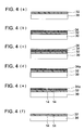
- FIGS. 4( a ) to 4 ( f ) are views showing processes to form the small diameter portion.
- FIGS. 5( a ) to 5 ( e ) are views showing processes to form the large diameter portion.
- FIG. 6 is a schematic view showing the entire constitution of a liquid ejection apparatus constituted by employing an electric field assist type liquid ejection head.
- FIG. 7 is a cross-sectional view showing schematic constitution of the liquid ejection apparatus according to the present embodiment.
- FIG. 8 is a schematic view showing the electric potential distribution near the ejection hole of a nozzle.
- FIG. 9 is a view showing the relationship between the electric field intensity at the tip portion of a meniscus and the thickness of the small diameter portion.
- FIG. 10 is a view showing the relationship between the electric field intensity at the tip portion of a meniscus and the nozzle diameter.
- FIG. 11 is a view showing one example of the drive control of a liquid ejection head.
- FIGS. 12( a ) to 12 ( c ) are views showing a variant example of drive voltage applied to a piezoelectric element.
- FIG. 1 schematically shows nozzle plate 1 , body plate 2 , and piezoelectric elements 3 which constitute an ink-jet system recording head (hereinafter referred to as recording head) A, which is an example of a liquid ejection head.
- recording head ink-jet system recording head
- nozzle plate 1 arranged is a plurality of nozzles 11 to eject ink. Further, in body plate 2 , via adhesion of nozzle plate 1 , formed are pressurizing chamber grooves 24 each converted to a pressurizing chamber, ink feeding channel grooves 23 each converted to an ink feeding channel, common ink chamber groove 22 converted to a common ink chamber, and ink feeding opening 21 .
- channel unit M is formed via adhesion of nozzle plate 1 and body plate 2 so that nozzles 11 of nozzle plate 1 and pressurizing chamber grooves 24 of body plate 2 correspond one to one.
- each symbol of the pressurizing chamber groove, the feeding channel groove and the common ink chamber groove, which are employed in the above description, is also employed for each of the pressurizing chamber, the feeding channel and the common ink chamber.
- FIG. 2 schematically shows the cross-section at Y-Y position of nozzle plate 1 and X-X position of body plate 2 , after nozzle plate 1 , body plate 2 , and piezoelectric element 3 are assembled in above recording head A.
- recording head A is completed via adhesion of piezoelectric element 3 , as an actuator for ink ejection, onto the surface of bottom portion 25 of each pressurizing chamber 24 , which is opposite the surface of body plate 2 adhered by nozzle plate 1 .
- FIG. 3 shows the cross-section of one of nozzles 11 .
- Nozzle 11 is formed by drilling into nozzle plate 1 .
- Each nozzle 11 is of a two-step structure composed of small diameter portion 14 having ejection hole 13 at ejection surface 12 and large diameter portion 15 , located backward, having a larger diameter than small diameter portion 14 , of each nozzle plate 1 .
- the length of small diameter portion 14 corresponds to the nozzle length in nozzle plate 1 . It is necessary to accurately make the above nozzle length in the same manner as that the diameter of ejection hole 13 which is an aperture of small diameter portion 14 is realized.
- 30 represents an Si substrate which is a first base material
- 32 represents a second base material in which small diameter portion 14 is formed
- 45 represents a liquid repellent layer.
- FIGS. 4 and 5 schematically show an outline of the manufacturing processes of nozzle plate 1 by employing cross-sections, while FIG. 5( d ) shows a completed nozzle plate. Further, FIG. 5( e ) shows a nozzle plate preferably provided with liquid repellent layer 45 .
- small diameter portion 14 which is employed as a first process, will be described with reference to FIG. 4 .
- a substrate to be converted to nozzle plate 1 one side of a first base material is provided with a second base material.
- second base material 32 On Si substrate 30 which is the first base material, arranged is second base material 32 which forms small diameter portion 14 ( FIG. 4( a )). It is necessary that the Si etching rate of components of second base material 32 during Si anisotropic dry etching is lower than that of Si etching. Further, preferred are materials capable of forming holes of about 1-about 10 ⁇ m via etching.
- etching materials such as SiO 2 or Al 2 O 3 , metals such as Ni or Cr, and resins such as a photoresist.
- SiO 2 and Al 2 O 3 each is about 1/300-about 1/200
- Ni and Cr each is about 1/500
- resins such as a photoresist are about 1/50.
- an etching rate ratio wherein the Si rate is 1 is designated as the etching selection ratio. Since these etching selection ratios vary depending on etching conditions such as the etching apparatus or the etching rate, they are represented by an approximate value. As its numerical value decreases, it becomes possible to realize the predetermined length of small diameter portion 14 at desired accuracy.
- second base material 32 of a thickness which is identical to the length and thickness of small diameter portion 14 , is arranged on Si substrate 30 by employing the above materials
- forming methods are not particularly limited and include a vacuum deposition method, a sputtering method, a CVD method, and a spin coating method. Any of these methods may appropriately be selected.
- the second base material is composed of SiO 2 , one may be employed which is prepared by thermally oxidizing silicon substrate 30 . Thickness of the second base material is not particularly limited. However, when it is excessively thick, channel resistance of nozzle 11 increases to raise drive voltage which is necessary for liquid droplet ejection. On the other hand, when it is excessively thin, strength is concerned. Consequently, it may appropriately be set to meet requirements.
- film 34 such as a Ni film, which is converted to etching mask 34 a , is arranged on second base material 32 via a conventional vacuum deposition or sputtering method ( FIG. 4( b )).
- Film 34 is not particularly limited as long as it becomes an etching mask during etching second base material 32 .
- photoresist pattern 36 via a prior art photolithographic process (resist coating, exposure and development) to form etching mask 34 a to form ejection hole 13 and small diameter portion 14 via a prior art photolithographic technology ( FIG. 4( c )).
- any portions which are not masked are removed via a conventional reactive dry etching method employing chlorine gas to achieve patterning, whereby etching mask 34 a is prepared. Thereafter, residual photoresist pattern 36 is removed via a conventional ashing method employing oxygen plasma ( FIG. 4( d )).
- small diameter portion 14 which passes through second base material 32 , is formed via a conventional reactive dry etching method employing CF 4 gas ( FIG. 4( e )).
- CF 4 gas FIG. 4( e )
- small diameter portion 14 is completed in the SiO 2 layer, namely second base material 32 ( FIG. 4( f )).
- second base material 32 When second base material 32 is converted to a photoresist, formation of a photoresist pattern automatically results in formation of small diameter portion 14 . Further, when second base material 32 is composed of metals such as Ni or Cr, it is possible to form small diameter portion 14 via dry etching employing oxygen plasma after forming a photoresist pattern on second base material 32 .
- large diameter portion 15 is formed by employing Si substrate 30 provided with second base material 32 , in which small diameter portion 14 is formed, and enables communicates with small portion 14 .
- a diameter is realized which is capable of having a thickness which assures enough durability of partitions so that interference of applied pressure to the liquid, for example in the adjacent nozzles of large diameter portion 15 results in no problem. Further, it is preferable that appropriate determination is made while considering the pitch of intervals of small diameter portion 14 .
- film 40 to be converted to an etching mask to arrange large diameter portions 15 via a conventional photolithographic process.
- film 40 is not particularly limited as long as it is converted to an etching mask during application of Si anisotropic dry etching to Si substrate 30 , and an example thereof includes an SiO 2 film.
- photoresist pattern 42 via conventional photolithographic technology ( FIG. 5( a )).
- etching mask 40 a of SiO 2 via a conventional reactive dry etching method employing CHF 3 gas.
- large diameter portions 15 in such a manner that penetration is achieved from the opposite surface on the side wherein small diameter portions 14 of Si substrate 30 are formed to at least small diameter portions 14 which are formed on the second base material and the entire cross-section of small diameter portions 14 is exposed.
- components of second base material 32 where small diameter portions are formed, exhibit a small etching selection ratio. Due to the above, during etching of large diameter portions 15 , after etching reaches second base material 32 , the resulting etching rate of second base material 32 decreases depending on the etching selection ratio.
- etching amount for example, when identical etching conditions are employed, it may be replaced by etching duration
- etching duration for example, when identical etching conditions are employed, it may be replaced by etching duration
- the etching selection ratio is small like as about 1/300-about 1/200.
- it is temporarily 1/200 in the case of an over-etching amount of 10 ⁇ m, it is possible to retard the shortened amount of small diameter portion 14 under the over-etching amount to approximately 0.05 ⁇ m.
- small diameter portion 14 passes through second base material 32 , by forming large diameter portion 15 under the over-etching state as described above, large diameter portion 15 and small diameter portion 14 are communicated, whereby a targeted nozzle is completed in which the length of small diameter portion 14 is approximately identical to the thickness of the second substrate ( FIG. 5( c )). Thereafter, photoresist pattern 42 and etching pattern 40 a are removed, whereby a nozzle plate is completed ( FIG. 5( d )). Photoresist pattern 42 may be removed immediately after formation of etching mask 40 a.
- the order of the first process to form small diameter portion 14 and the second process to form large diameter portion 15 may be replaced. Namely, as shown in FIG. 5 , initially, large diameter portion 15 is formed on Si substrate 30 provided with second base material 32 by employing an Si anisotropic dry etching method in the same manner as above. In this case, small diameter portion 14 is not yet formed on the second base material. Subsequently, as shown in FIG. 4 , on Si substrate 30 (in FIG. 4 , large diameter portion 15 is not shown) provided with large diameter portion 15 , small diameter portion 14 may be formed to pass through second base material 32 in the same manner as above.
- liquid repellent layer 45 is arranged on the surface on the side on which ejection holes of Si substrate 30 are formed ( FIG. 5( e )). Thereafter, after applying liquid repellent layer 45 on the surface on the side of Si substrate 30 through which ejection holes are formed ( FIG. 5( e )), division is made to individual plates 1 employing a dicer.
- Ejection surface 12 of nozzle plate 1 is flattened. By flattening ejection surface 12 , processing of nozzle plate 1 becomes easy, and when employed while being incorporated in a recording head, it is possible to more easily carry out cleaning via wiping of ejection surface 12 where ejection hole 13 exists without any problem.
- Liquid repellent layer 45 will now be described. It is preferable that liquid repellent layer 45 is arranged on the ejection surface where ejection hole 13 of nozzle plate 1 shown in FIG. 1 exists. By so arranging liquid repellent layer 45 , it is possible to retard oozing and spreading of liquid from ejection hole 13 due to soaking on ejection surface 12 . In practice, for example, when liquid is aqueous, water repellent materials are employed, while when liquid is oily, oil repellent materials are employed.
- fluororesins such as FEP (ethylene tetrafluoride and propylene hexafluoride), PTFE (polytetrafluoroethylene), fluorocyloxane, fluoroalkylsilane, or an amorphous perfluororesin, any of which is filmed on ejection surface 12 via a method such as coating or deposition.
- Thickness of the thin film is not particularly limited. However, the employed thickness is preferably less than 100 nm since it is possible to reduce effects to the substantial nozzle length.
- liquid repellent layer 45 it is possible to preferably employ one composed of a fluoroalkylsilane based monomolecular film.
- the film is formed on entire ejection surface 12 except nozzle hole 13 of nozzle 11 .
- Fluoroalkylsilanes include those represented by the following formula. R—Si—X 3 wherein X represents a hydrolyzable group which is preferably an alkoxy group having 1-5 carbon atoms, while R represents a fluorine-containing organic group which is preferably a fluoroalkyl group having 1-20 carbon atoms.
- liquid repellent layer 45 may be formed directly on ejection surface 12 of nozzle plate 1 , or via an intermediate layer to enhance closer adhesion of liquid repellent layer 45 .
- the cross-sectional shape nozzle 11 is not limited to a circular shape, and instead of the circular shape, a cross-sectional polygon shape or a cross-sectional star shape may be acceptable.
- the cross-sectional shape is not circular, for example, the term “large diameter greater than small diameter” means that the diameter of a circle which has the same area as that of the large diameter portion is greater than the diameter of a circle which has the same area as that of the small diameter portion.
- body plate 2 is provided with a plurality of pressurizing chamber grooves 24 converted to pressurizing chambers, each of which communicates with nozzle 11 , a plurality of ink feeding grooves 23 converted to ink feeding channels, each of which communicates with the above pressurizing chamber, common ink chamber groove 22 converted to a common ink chamber which communicates with the above ink feed, and ink feeding opening 21 .
- These grooves are formed, for example, on a specially prepared Si substrate via a conventional photolithographic process (resist coating, exposure and development) and an Si anisotropic dry etching technology, whereby body plate 2 is prepared.
- Channel unit M is formed via adhesion of nozzle plate 1 and body plate 2 so that nozzles 11 of nozzle plate 1 and pressurizing chamber grooves of body plate 2 correspond one-to-one.
- Recording head A is completed via adhesion of piezoelectric element 3 , as an actuator for ink ejection, to the rear surface of bottom portion 25 of each pressurizing chamber 24 opposite the surface adhered by nozzle plate 1 of body plate 2 .
- nozzle plate 1 described above, to the so-called electric field assist type liquid ejection head which ejects liquid droplets utilizing action of electrostatic force.
- FIG. 6 schematically shown is the overall constitution of liquid ejection apparatus 60 which is constituted by employing electric field assist type liquid ejection head B (liquid ejection head B).
- Charging electrode 50 which is composed of electrically conductive components such as NiP, Pt, or Au, and which is an electrostatic voltage applying means to charge liquid into the nozzle, is arranged, for example, on the inner peripheral surface of large diameter portion 15 of nozzle plate 1 which is employed in liquid ejection head B. By arranging charging electrode 50 , above charging electrode 50 is brought into contact with liquid in large diameter portion 15 of nozzle plate 1 .
- liquids which are ejected to form droplets may be inorganic liquids such as water, organic liquids such as methanol, and electrically conductive pastes which incorporate a large amount of materials (such as silver powder) of high electrical conductivity.
- piezoelectric element 3 which is a piezoelectric element actuator as a pressure generating means.
- Piezoelectric element 3 is connected to drive voltage power source 52 so that drive voltage is applied to piezoelectric element 3 to deform piezoelectric element 3 .
- Piezoelectric element 3 is deformed via application of drive voltage from drive voltage power source 52 so that liquid in the nozzle is pressurized to form a meniscus of the liquid at ejection hole 13 of nozzle 11 .
- liquid repellent layer 45 on ejection surface 12 in the presence of ejection hole 13 , it is possible to effectively minimize any decrease in electric field concentration to the meniscus tip portion due to spread of the liquid meniscus formed in the nozzle ejection hole 13 portion, over ejection surface 12 in the periphery of ejection hole 13 .
- 55 is a control section which controls liquid ejection apparatus 60 such as drive voltage power source 52 or electrostatic voltage power source 51 .
- an electric field assist type liquid ejection head capable of efficiently ejecting liquid droplets via synergic effects of the pressure applied to the liquid via piezoelectric element 3 and the electrostatic attractive force to the liquid via charging electrode 50 .
- FIG. 7 is a cross-sectional view showing the entire constitution of the liquid ejection apparatus according to the first embodiment.
- liquid ejection head 102 and liquid ejection apparatus 101 it is possible to apply liquid ejection head 102 and liquid ejection apparatus 101 to various liquid ejection apparatuses such as so-called serial or line systems.
- Liquid ejection apparatus 101 incorporates liquid ejection head 102 , incorporating a plurality of nozzles 110 , each of which ejects liquid droplet D of liquid L such as an electrically chargeable ink, and counter electrode 103 which not only carries a facing surface which faces nozzles 110 of liquid ejection head 102 but also supports base material K which results in deposition of liquid droplet D on its facing surface.
- liquid L such as an electrically chargeable ink
- nozzle plate 111 which is employed in liquid ejection head 102 and in which a plurality of nozzles 110 is formed which ejects liquid droplets from ejection hole 113 .
- Nozzle plate 111 according to the present embodiment is provided with SiO 2 film 111 b and liquid repellent film 111 c at a thickness of less than 100 nm in the above order on one surface on counter electrode 103 side of silicon substrate 111 a .
- nozzles 110 formed on nozzle plate 111 are formed as a two-step structure provided with large diameter portion 115 which passes through silicon substrate 111 a , and small diameter portion 114 which passes through both SiO 2 film 111 b and liquid repellent film 111 c .
- liquid ejection head 102 is constituted as a head carrying a flat ejection surface so that nozzles 110 do not project from ejection surface 112 which faces counter electrode 103 of nozzle plate 111 and base material K.
- Small diameter portion 114 and large diameter portion 115 of each nozzle 110 are formed to be columnar.
- the internal diameter of small diameter portion 114 becomes at most 10 ⁇ m, and the dimensions of portions other than nozzles 110 may be appropriately set as required.
- liquid repellent film 128 On the nozzle plate, formed is liquid repellent film 128 .
- One example of its forming method includes a method while ejecting air from nozzles 110 so that liquid repellent agents result in no penetration into nozzles 110 , a coating liquid, in which fluoroalkylsilane is dissolved, is applied and dried and thereafter, the resulting coating is sufficiently sintered to form a monomolecular film.
- forming methods of liquid repellent film 128 are not particularly limited, and it is possible to prepare the film by employing methods such as a coating method employing rollers such as a reverse roller coater, a coating method employing blades, or a CVD (Chemical Vapor Deposition) method. Further, in order to minimize penetration of liquid repellent agents into nozzles 110 , it may be acceptable that a film is prepared in such a state in which liquid L is filled in nozzles 110 .
- charging electrode 116 On the surface on the side opposite ejection surface 112 of nozzle plate 111 , arranged is laminated charging electrode 116 composed of electrically conductive components such as NiP, to charge liquid L in nozzles 110 .
- charging electrode 116 is arranged to reach internal peripheral surface 117 of large diameter portion 115 of nozzle 110 to come into contact with liquid L in the nozzle.
- charging electrode 116 is connected to charging voltage power source 118 as an electrostatic voltage applying means which applies electrostatic voltage to generate an electrostatic attractive force.
- charging electrodes 116 is individually brought into contact with liquid L in each of nozzles 110 , whereby when electrostatic voltage is applied to charging electrodes 116 from charging voltage power source 118 , liquid L in all nozzles 110 is simultaneously charged so that an electrostatic attractive force is generated between liquid L in nozzles 110 or cavities 120 described below and base material K supported by counter electrode 103 .
- body plate 119 In the rear of charging electrodes 116 , arranged is body plate 119 . In the portion facing the aperture edge of large diameter portion 115 of each nozzle 110 of body plate 119 , formed is an approximately cylindrical space having the approximately identical inner diameter at each aperture edge, and each space is employed as cavity 120 to temporarily store liquid L ejected from ejection hole 113 of nozzles 110 .
- flexible layer 121 composed of a thin metallic plate and silicon, which exhibit flexibility, and via flexible layer 121 , liquid L in liquid ejection head 102 is prevented from no leaking to the exterior.
- body plate 119 formed are channels, not shown, to feed liquid L to cavities 120 .
- a silicon plate as body plate 119 is etched whereby cavities 120 , a common channel, not shown, and channels which connect the common channel with cavities 120 are arranged.
- the common channel is connected with a feeding pipe, not shown, which feeds liquid L from a liquid tank, not shown, on the exterior, and an arrangement is made so that a specified feeding pressure is applied to liquid L in the channels, cavities 120 , and nozzles 110 via a feeding pump, not shown, or differential pressure due to the arranged position of the liquid tank.
- piezoelectric element 122 which is a piezoelectric element actuator as each of the pressure generating means.
- Piezoelectric element 122 is electrically connected to drive voltage power source 123 to deform the above element via application of drive voltage to the above element.
- Piezoelectric element 122 is deformed via applied drive voltage from drive voltage power source 123 to allow liquid L in nozzles to generate pressure, whereby a meniscus of liquid L is formed at ejection hole 113 of each nozzle 110 .
- the piezoelectric element actuator as employed in the present embodiment, it is possible to employ, for example, an electrostatic actuator or a thermal system.
- Drive voltage power source 123 and aforesaid charging voltage power source 118 each is connected to operation control means 124 and each is controlled via operation control means 124 .
- operation control means 124 is composed of a computer which is constituted in such a manner that CPU 125 and ROM 126 , and RAM 127 , are connected via BUS, not shown. An arrangement is made as follows.
- CPU 125 drives charging voltage power source 118 and each drive voltage power source 123 , based on power source control programs stored in ROM 126 so that liquid L is ejected from ejection hole 113 of nozzles 110 .
- operation control means 124 controls application of electrostatic voltage to above charging electrode 116 via charging voltage power source 118 which is an electrostatic voltage applying means so that liquid L in nozzles 110 and cavities 120 is charged to generate an electrostatic attractive force between liquid L and base material K. Further, based on power source control programs, operation control means 124 drives each drive voltage power source 123 to deform each piezoelectric element 122 , followed by to generation of pressure in liquid L in nozzles 110 so that a meniscus of liquid L is formed at ejection hole 113 of each nozzle 110 .
- tabular counter electrode 103 which supports base material K on the rear surface, in parallel with ejection surface 112 of liquid ejection head 102 , while being separately arranged at a predetermined distance.
- the separate distance between counter electrode 103 and liquid ejection head 102 is appropriately set to be in the range of about 0.1-about 3 mm.
- counter electrode 103 is grounded and is always maintained at ground potential. Due to that, when electrostatic voltage is applied to charging electrode 116 from above charging voltage power source 118 , potential difference is formed between liquid L in ejection hole 113 of nozzle 110 and the surface facing liquid ejection head 102 of counter electrode 103 , whereby an electric field is generated. Further, when charged liquid droplet D is deposited onto base material K, counter electrode 103 lets out the resulting electric charges via grounding. In addition, grounding methods of counter electrode 103 are not limited to the present embodiment. Charging electrode 116 may be grounded, and electrostatic voltage may be applied to counter electrode 103 .
- Counter electrode 103 or liquid ejection head 102 is provided with a positioning means, not shown, which achieves positioning by relatively displacing liquid ejection head 102 and base material K.
- a positioning means not shown, which achieves positioning by relatively displacing liquid ejection head 102 and base material K.
- liquid L capable of being ejected from liquid ejection apparatus 101
- employed may be conventional liquids without any specific limitation.
- liquid L it is possible to employ electrically conductive pastes which incorporate a large amount of compounds of high electrical conductivity such as silver powders. Still further, targeted compounds, which are employed to be dissolved or dispersed in above liquid L, are not particularly limited, as long as coarse particles which generate clogging of nozzles are removed.
- phosphors compounds which are conventionally known as phosphors, which are employed in PDP (Plasma Display Panel), CRT (Cathode Ray Tube), or FED (Field Emission Display).
- red phosphors listed are (Y,Gd) BO 3 :Eu and YO 3 :Eu; as green phosphors listed are Zn 2 SiO 4 :Mn, BaAl 12 O 19 :Mn, and (Ba,Sr,Mg)O- ⁇ -Al 2 O 3 :Mn; and as blue phosphors listed are BaMgAl 14 O 23 :Eu and BaMgAl 10 O 17 :Eu.
- binders employed may be conventional resin compounds without any specific limitation. Resin compounds include not only homopolymers but also those which are blended within their compatible range.
- liquid ejection apparatus 101 When liquid ejection apparatus 101 is employed as a patterning means, it is possible to employ it for the use of display as representative one.
- listed may be formation of PDP phosphors, formation of PDP ribs, formation of PDP electrodes, formation of CRT phosphors, formation of FED phosphors, formation of FED ribs, formation of color filters such as an RBG colored layer for LCD (Liquid Crystal Display) and a black matrix layer, and formation of spacers for LCD such as a pattern corresponding to a black matrix and a dot pattern.
- “Rib”, as described herein, generally means a barrier, and when PDP is taken as an example, it is employed to separate the plasma region of each color.
- Other uses of the present embodiment may include micro-lenses, patterning coating of magnetic materials, ferroelectric materials, and electrically conductive pastes which are converted to wiring or antenna, as uses for semiconductors, normal printing, printing onto special media such as film, cloth, and steel plate, curved surface printing, press plates of various printing plates, as graphic uses, coating of adhesive materials and sealing materials, as processing uses, and coating of medical products in which a plurality of minute components is blended and samples for gene diagnosis, as bio and medical uses.
- electrostatic voltage is applied to charging electrode 116 from charging voltage power source 118 so that an electric field is generated between liquid L in ejection hole 113 of all nozzles 110 and the surface facing liquid ejection head 102 of counter electrode 103 .
- drive voltage is applied to piezoelectric element 122 corresponding to each nozzle 110 to eject liquid L via drive voltage power source 123 to deform piezoelectric element 122 , whereby a meniscus of liquid L in ejection hole 113 of nozzles 110 is formed via the pressure applied to liquid L (refer to FIG. 8 ).
- equal electric potential lines are formed in approximately the vertical direction in the interior of nozzle plate 111 to ejection surface 112 , and a strong electric field is generated which directs to liquid L in small diameter portion 114 of nozzle 110 and meniscus M.
- the identical potential lines at the tip portion of the meniscus M are dense, and at the tip portion of meniscus M, the electric field is significantly concentrated. Consequently, meniscus M is torn off due to a strong electrostatic force of the electric field, followed by separation from liquid L in the nozzle to form liquid droplet D. Further, resulting liquid droplet D is accelerated via an electrostatic force and attracted by base material K supported by counter electrode 103 , to achieve deposition. At that time, since liquid droplet D tends to be deposited onto the nearer position, the angle to base material K during deposition is stabilized, whereby accurate deposition is achieved.
- liquid ejection head 102 As described above, by utilizing the ejection principle of liquid L in liquid ejection head 102 according to the present embodiment, even in liquid ejection head 102 having a flat ejection surface, it is possible to achieve high electric field concentration by employing nozzle plate 111 with high volume resistance and by generating electric potential difference in the vertical direction to ejection surface 112 , whereby an accurate and stable ejection state of liquid L is achieved. Further, it is possible to assuredly and appropriately form meniscus M via liquid repellent film 111 c and to reduce fluctuation of the nozzle length in small diameter portion 114 , whereby it is possible to enhance ejection performance.
- the inventors of the present invention conducted experiments and simulation experiments employing nozzle plate 111 composed of various insulators. As a result, it was found that the electric field intensity at the tip portion of meniscus M depended on the nozzle diameter and the thickness of insulators, and the electric field intensity, which was necessary for liquid droplet ejection, was approximately 1.5 ⁇ 10 7 V/m. In more detail, it is possible to realize the concentrated electric field intensity which is necessary for electric field concentration ejection in such a manner that based on to FIGS.
- the thickness of insulating SiO 2 film 111 b is set to be at equal to or more than 45 ⁇ m, and when the nozzle diameter is 5 ⁇ m, the thickness of SiO 2 film 111 b is set to be at equal to or more than 20 ⁇ m, while when the nozzle diameter is 2 ⁇ m, the thickness of SiO 2 film 111 b is set to be at equal to or more than 5 ⁇ m.
- simulation experiments were conducted employing simulation via an electric current distribution analysis mode in “PHOTO-VOLT” (being a trade name, produced by Photon Co., Ltd.), which is an electric field simulation software.
- FIG. 11 is a view to describe a drive control of the liquid ejection head in the liquid ejection apparatus according to the present embodiment.
- constant electrostatic voltage Vc is applied to charging electrode 116 from charging voltage power source 118 via operation control means 124 of liquid ejection apparatus 101 .
- constant electrostatic voltage Vc is always applied to each nozzle 110 of liquid ejection head 102 , whereby an electric field is generated between liquid L in liquid ejection head 102 and base material K supported by counter electrode 103 .
- piezoelectric element 122 which corresponds to each nozzle 110 to eject liquid droplet D
- piezoelectric element 122 is deformed whereby pressure of liquid L in the nozzle increases and in ejection hole 113 of nozzle 110 , meniscus M is lifted up from the state A in FIG. 11(A) , and as sate B in FIG. 11 shows, a state is formed in which meniscus M is significantly lifted up.
- fluorinated alkylsilane repellent film 111 c is formed on ejection surface 112 of nozzle plate 111 , meniscus M formed in ejection hole 113 of each nozzle 110 is not spread onto ejection surface 112 , whereby lifted meniscus M is maintained.
- liquid droplet D tends to be deposited onto the nearer position via the action of electrostatic force.
- the deposition direction to base material K is not deviated, and stable deposition is accurately carried out onto base material K.
- state D in FIG. 11(D) shows, in nozzles 110 , the liquid surface results in setback by the torn-off amount, but liquid L is replenished from cavity 120 followed by rapid return to the state A of FIG. 11 .
- drive voltage V D applied to piezoelectric element 122 it is possible to make it a pulse voltage as employed in the present embodiment.
- a voltage such as so-called triangular voltage is applied in which after gradual increase in voltage, it gradually decreases a trapezoidal voltage is applied in which after gradual increase in voltage, it is once kept at a constant value and thereafter gradually decreases, or a sine wave voltage is applied.
- it may be constituted in such a manner that as shown in FIGS.
- nozzle plate 111 and liquid ejection apparatus 102 As described above, by employing nozzle plate 111 and liquid ejection apparatus 102 according to the present embodiment, even in nozzles 110 each having small ejection hole 113 at an internal diameter of small diameter portion 114 of less than 10 ⁇ m and by forming liquid repellent film 111 c at a thickness of less than 100 nm, it is possible to minimize fluctuation of the nozzle diameter due to entrance of liquid repellent film 111 c into ejection hole 113 , and in addition, to retard fluctuation of the nozzle length due to fluctuation of thickness of liquid repellent film 111 c , whereby it is possible to avoid adverse effects to the ejection of liquid droplets.
- liquid repellent film 111 c is formed to be thinner, it is possible to make the nozzle length shorter, whereby it is possible to retard an increase in channel resistance in nozzles 110 , and also to retard an increase in pressure applied to liquid L in nozzles 110 during ejection of liquid droplets.
- liquid repellent film 111 c since via liquid repellent film 111 c , it is possible to avoid spread of liquid L from ejection hole 113 of nozzles 110 and adhesion of ejected liquid droplet D to ejection surface 112 , the electric field intensity at the tip portion of meniscus M is not disturbed, whereby it is possible to further enhance ejection performance.
- nozzles 110 carrying small ejection hole 113 at an internal diameter of the small diameter portion of less than 10 ⁇ m, it is possible to employ them in an electric field concentration system liquid ejection heads for highly concentrated electric field intensity.
- fluorosilane based liquid repellent film 111 c on the ejection surface side of SiO 2 film 111 b , it is possible to convert it to a preferred monomolecular film. Further, by employing fluorosilane based liquid repellent film 111 c , it is possible to convert it to nozzle plate 111 which results in no change of repellency with age.
- constitution is made so that meniscus M is lifted up via deformation of piezoelectric element 122 .
- Any pressure generating means may be employed which is capable of lifting up meniscus M as described above.
- constitution may be acceptable in which, for example, air bubbles are formed by heating liquid L in nozzles 110 and cavities 120 and the resulting pressure is utilized.
- counter electrode 103 is grounded.
- a constitution is also employable in which, for example, voltage is applied to counter electrode 103 from the power source and the power source is controlled via operation control means 124 so that electric potential difference reaches the predetermine value such as 1.5 kV.
- FIGS. 4 and 5 An example to manufacture nozzle plate 1 will now be described, employing FIGS. 4 and 5 . Initially, formation of small diameter portions 14 is described with reference to FIG. 4 . On one surface of 200 ⁇ m thick Si substrate 30 , formed was a 5 ⁇ m thick SiO 2 film as second base material 32 ( FIG. 4( a )). Plasma CVD was employed as the forming method.
- a 0.3 ⁇ m thick Ni film which was film 34 converted to etching mask 34 a was formed via a sputtering method ( FIG. 4( b )).
- photoresist pattern 36 On the Ni film was formed photoresist pattern 36 via a photolithographic process ( FIG. 4 c )).
- etching mask 34 a By employing etching mask 34 a , the SiO 2 film, which was second base material 32 , was subjected to dry etching in which CF 4 was employed as the reaction gas, whereby small diameter portions 14 were formed ( FIG. 4( e )).
- the etching amount to form small diameter portions 14 was obtained via preliminary experiments. However, upon considering the fluctuation range of the etching amount, 5.5 ⁇ m was employed while increased by 0.5 ⁇ m (10%). By increasing the etching amount by 10%, small diameter portions 14 resulted in a state in which the SiO 2 film, which was second base material 32 , was passed trough. Though over-etching of the above small diameter potions 14 affects Si substrate 30 , no problem occurs by later arranging large diameter portions 15 on the side of Si substrate 30 .
- etching mask 40 a Si substrate 30 was subjected to Si anisotropic dry etching, whereby large diameter portions 15 were formed.
- the etching amount to form large diameter portions 15 was previously determined via experiments, and upon considering the fluctuation range of the etching amount, 210 ⁇ m was determined. Further, the SiO 2 etching selection ratio, which was previously obtained via experiments, was 1/200. Accordingly, when 200 ⁇ m thick Si substrate 30 was subjected to Si anisotropic dry etching, excess length of the large diameter portion due to over-etching to the SiO 2 second base material, in which small diameter portions 14 were formed, became 0.05 ⁇ m. As a result, a nozzle hole was completed in which large diameter portion 15 was passed through small diameter portion 14 without any problem and the length of small diameter portion 14 (being the nozzle length) was almost as specified ( FIG. 5( c )).
- RIE reactive ion etching method
- liquid repellent processing agent a 1% trichlorotrifluoroethane solution of undecafluoropentyltrimethoxysilane was prepared and applied onto the SiO 2 film where the small diameter portions were formed. Thereafter, heating at 120° C. for 30 minutes was carried out, whereby liquid repellent film was formed ( FIG. 5( e )).
- Si substrate 30 carrying the nozzle holes, formed via the above steps, was separated via a dicing saw, whereby nozzle plate 1 , carrying nozzle holes, was prepared.
- body plate 2 shown in FIG. 1 , was produced.
- the Si substrate formed were a plurality of pressurized chamber grooves converted to pressurized chambers, each of which communicated with the nozzle, a plurality of ink feeding grooves converted to ink feeding channels, each of which communicated with the above pressurized chamber, a common ink chamber groove converted to a common ink chamber which communicated with the above ink feed, and an ink feeding hole, by employing a conventional photolithographic process (resist coating, exposure, and development) as well as Si anisotropic dry etching technology.
- a conventional photolithographic process resist coating, exposure, and development
- nozzle plate 1 and body plate 2 prepared as above, were adhered to each other via adhesives, and further, piezoelectric element 3 , which was a pressure generating means, was fitted to the rear surface of each pressurized chamber 24 of body plate 2 , whereby liquid droplet ejection head A was prepared.
- piezoelectric element 3 which was a pressure generating means
- the liquid ejection apparatus according to the present invention was prepared by employing each of the nozzle plates in which the thickness of the SiO 2 film, where the small diameter portions were formed and the diameter of the small diameter portions in Example 1 were variously changed (Embodiment 1 in Table 1). Incidentally, 16 nozzles were formed in one nozzle plate.
- liquid ejection apparatus was prepared employing a nozzle plate in which the liquid repellent film was replaced with a 2 ⁇ m thick one employing fluorine based liquid repellent agents (Embodiment 2 in Table 1).
- a liquid to be ejected was an ink incorporating 52% by weight of water, 22% by weight of ethylene glycol, 22% by weight of propylene glycol, 3% by weight of a dye (CI Acid Red 1), and 1% by weight of surface active agents. Further, the ejection performance was evaluated as follows. Initially, after continuously driving all liquid ejection heads over 24 hours, the drive voltage of the piezoelectric element was gradually increased while applying constant electrostatic voltage (1.5 kV), and voltage (hereinafter referred to as “limit drive voltage”) to initiate ejection of liquid droplets from each nozzle was determined.
- limit drive voltage constant electrostatic voltage
Landscapes
- Engineering & Computer Science (AREA)
- Manufacturing & Machinery (AREA)
- Particle Formation And Scattering Control In Inkjet Printers (AREA)
Abstract
Description
(2) A small cross-sectional nozzle is formed from one side of the silicon substrate via dry etching and a part of a large cross-sectional nozzle and a part of a cross-section of an ink chamber provided with an ink chamber communicated with the large cross-sectional nozzle, a pressurizing chamber, and an ink feeding channel are subjected to dry etching from the other side of the silicon substrate to communicate with the small cross-sectional nozzle, whereby a nozzle is formed (refer to Patent Document 2).
(3) A buffer layer, which exhibits a lower etching rate compared to a single crystal silicon wafer, is sandwiched between two single crystal silicon wafers to result in integration via close adhesion and both sides of the integrated two single crystal silicon wafers are subjected to etching so that the bottom portion forms holes, each of which reaches the buffer layer. Thereafter, etching is applied to the side on which the bottom diameter of the hole of the buffer layer is smaller, whereby a nozzle hole is formed (refer to Patent Document 3).
- Patent Document 1: Japanese Patent Publication Open to Public Inspection (hereinafter referred to as JP-A) No. 11-28820
- Patent Document 2: JP-A No. 2004-106199
- Patent Document 3: JP-A No. 6-134994
- Patent Document 4: JP-A No. 5-229130
- Patent-Document 5: JP-A No. 2003-341070
a manufacturing method of a nozzle plate for a liquid ejection head, wherein
a process which prepares a substrate which is composed in such a manner that on one side of a first base material composed of Si, a second base material is arranged which exhibits a lower etching rate than Si during Si anisotropic dry etching,
a process which forms, on the surface of the aforesaid second base material, a film which is converted to a second etching mask,
a process which forms a second etching mask pattern having the aperture shape of the aforesaid small diameter portion by applying a photolithographic treatment and etching to the aforesaid film which is converted to the second etching mask, a process which carries out etching until the aforesaid second base material is passed through,
a process which forms, on the surface of the aforesaid first base material, a film which is converted to a first etching mask,
a process which forms a first etching mask pattern having an aperture shape of the aforesaid large diameter portion by applying a photolithographic process and etching to the aforesaid film which is converted to the first etching mask, and
a process which carries out Si anisotropic dry etching until the aforesaid first base material is passed through, are carried out in the above order.
2. In a manufacturing method of a nozzle plate for a liquid ejection head, which is composed of a substrate having a through-hole,
which is composed of a large diameter portion open into the one side surface of the aforesaid substrate and a small diameter portion open into the other side surface, which has a smaller cross-section than that of the aforesaid large diameter portion, and in which the aperture of the aforesaid small diameter portion of the aforesaid through-hole is employed as a liquid droplet ejection hole,
a manufacturing method of a nozzle plate for a liquid ejection head, wherein
a process which prepares a substrate which is composed in such a manner that on one side of a first base material composed of Si, a second base material is arranged which exhibits a lower etching rate than Si during Si anisotropic dry etching,
a process which forms, on the surface of the aforesaid first base material, a film which is converted to a first etching mask,
a process which forms a first etching mask pattern having the aperture shape of the aforesaid large diameter portion by applying a photolithographic treatment and etching to the aforesaid film which is converted to the first etching mask, a process which carries out Si anisotropic dry etching until the aforesaid first base material is passed through,
a process which forms, on the surface of the aforesaid second base material, a film which is converted to a second etching mask,
a process to forms an etching mask pastern having the aperture shape of the aforesaid small diameter portion by applying a photolithographic treatment and etching to the film which is converted to a second etching mask, and
a process which carries etching until the aforesaid second base material is passed through,
are carried out in the above order.
3. The manufacturing method of a nozzle plate for a liquid ejection head, described in
4. The manufacturing method of a nozzle plate for a liquid ejection head, described in any one of
5. A nozzle plate for a liquid ejection head, which is composed of a substrate having a through-hole,
which is composed of a large diameter portion open into one side surface of the aforesaid substrate and a small diameter portion open into the other side surface of the aforesaid substrate,
in which the aperture of the aforesaid small diameter portion of the aforesaid though-hole is employed as a liquid droplet ejection hole,
wherein a substrate component which constitutes the aforesaid large diameter portion is Si,
and a substrate component which constitutes the aforesaid small diameter portion is composed of a component which exhibits a lower etching rate during Si anisotropic dry etching than that of the substrate component which constitutes the aforesaid large diameter portion.
6. The nozzle plate for a liquid ejection head, described in
7. The nozzle plate for a liquid ejection head, described in
8. The nozzle plate for a liquid ejection head, described in
9. The nozzle plate for a liquid ejection head, described in item 8, wherein the aforesaid liquid repellent layer is a fluoroalkylsilane based monomolecular layer.
10. The nozzle plate for a liquid ejection head, described in item 8 or 9, wherein the internal diameter of the aforesaid small diameter portion is less than 6 μm.
11. The nozzle plate for a liquid ejection head, described in item 8 or 9, wherein the internal diameter of the aforesaid small diameter portion is less than 4 μm.
12. In a liquid ejection head which is provided with a body plate in which a concave portion is formed and
a nozzle plate having a nozzle, the nozzle plate overlaying the aforesaid body plate in such a manner that the aforesaid concave portion is formed as a pressurizing chamber and is provided with a nozzle which communicates with the aforesaid pressurizing chamber by transmitting the displacement of a pressure generator to liquid in the aforesaid pressurizing chamber and ejects droplets of the aforesaid liquid from an ejection hole,
a liquid ejection head wherein the aforesaid nozzle plate is the nozzle plate for the liquid ejection head, described in any one of
13. The liquid ejection head, described in
R—Si—X3
wherein X represents a hydrolyzable group which is preferably an alkoxy group having 1-5 carbon atoms, while R represents a fluorine-containing organic group which is preferably a fluoroalkyl group having 1-20 carbon atoms.
| TABLE 1 | |||||
| Fluctuation of | Evaluation | ||||
| Small Diameter | Water | Piezoelectric | of Liquid | ||
| Experiment | Nozzle Diameter | portion length | Repellent | Element Drive | Droplet |
| No. | (φ μm) | (μm) | Film | Voltage (%) | |
| 1 | 1 | 20 | |
4 | A |
| 2 | 1 | 10 | |
7 | A |
| 3 | 1 | 5 | |
9 | A |
| 4 | 3 | 20 | |
5 | A |
| 5 | 3 | 10 | |
7 | A |
| 6 | 3 | 5 | |
8 | A |
| 7 | 5 | 20 | |
4 | A |
| 8 | 5 | 10 | |
7 | A |
| 9 | 5 | 5 | |
9 | A |
| 10 | 8 | 20 | |
5 | A |
| 11 | 8 | 10 | |
6 | A |
| 12 | 8 | 5 | |
7 | A |
| 13 | 10 | 20 | |
8 | A |
| 14 | 10 | 10 | |
8 | A |
| 15 | 10 | 5 | |
10 | A |
| 16 | 1 | 20 | |
39 | B |
| 17 | 1 | 10 | |
44 | B |
| 18 | 1 | 5 | |
49 | B |
| 19 | 3 | 20 | |
41 | |
| 20 | 3 | 10 | |
45 | |
| 21 | 3 | 5 | |
52 | |
| 22 | 5 | 20 | |
37 | |
| 23 | 5 | 10 | |
44 | |
| 24 | 5 | 5 | |
51 | |
| 25 | 8 | 20 | |
31 | B |
| 26 | 8 | 10 | |
34 | B |
| 27 | 8 | 5 | |
37 | B |
| 28 | 10 | 20 | |
33 | B |
| 29 | 10 | 10 | |
36 | |
| 30 | 10 | 5 | |
39 | B |
- A: fluctuation of the liquid droplet diameter was small
- B: some fluctuation of the liquid droplet diameter was noted, but resulted in no problem for commercial viability
- C: fluctuation of the liquid droplet diameter was significant and resulted in problems for commercial viability
Claims (7)
Applications Claiming Priority (5)
| Application Number | Priority Date | Filing Date | Title |
|---|---|---|---|
| JP2006-236050 | 2006-08-31 | ||
| JP2006236050 | 2006-08-31 | ||
| JP2006254126 | 2006-09-20 | ||
| JP2006-254126 | 2006-09-20 | ||
| PCT/JP2007/066022 WO2008026455A1 (en) | 2006-08-31 | 2007-08-17 | Method for manufacturing nozzle plate for liquid ejection head, nozzle plate for liquid ejection head, and liquid ejection head |
Publications (2)
| Publication Number | Publication Date |
|---|---|
| US20090195605A1 US20090195605A1 (en) | 2009-08-06 |
| US8881399B2 true US8881399B2 (en) | 2014-11-11 |
Family
ID=39135738
Family Applications (1)
| Application Number | Title | Priority Date | Filing Date |
|---|---|---|---|
| US12/310,380 Active 2030-02-10 US8881399B2 (en) | 2006-08-31 | 2007-08-17 | Method of manufacturing a nozzle plate for a liquid ejection head |
Country Status (5)
| Country | Link |
|---|---|
| US (1) | US8881399B2 (en) |
| EP (1) | EP2058132B1 (en) |
| JP (1) | JP5120256B2 (en) |
| CN (1) | CN101505967B (en) |
| WO (1) | WO2008026455A1 (en) |
Cited By (1)
| Publication number | Priority date | Publication date | Assignee | Title |
|---|---|---|---|---|
| US11925303B2 (en) | 2017-03-10 | 2024-03-12 | Sharkninja Operating Llc | Agitator with debrider and hair removal |
Families Citing this family (11)
| Publication number | Priority date | Publication date | Assignee | Title |
|---|---|---|---|---|
| US9044953B2 (en) * | 2009-08-28 | 2015-06-02 | Hewlett-Packard Development Company, L.P. | Hard imaging devices, print devices, and hard imaging methods |
| CN102120561B (en) * | 2010-01-08 | 2012-07-11 | 中芯国际集成电路制造(上海)有限公司 | Method for forming wafer through hole |
| JP2014100812A (en) * | 2012-11-17 | 2014-06-05 | Mimaki Engineering Co Ltd | Ink discharge system |
| JP6333992B2 (en) | 2013-12-26 | 2018-05-30 | 大連理工大学 | Integrated molding manufacturing method of liquid nozzle and liquid ejecting apparatus and apparatus therefor |
| US9561655B2 (en) * | 2015-01-16 | 2017-02-07 | Ricoh Company, Ltd. | Liquid discharging head, liquid discharging unit, and device to discharge liquid |
| JP2017043023A (en) * | 2015-08-27 | 2017-03-02 | エスアイアイ・プリンテック株式会社 | Ink jet head and liquid jet recording device |
| JP2017132244A (en) * | 2016-01-27 | 2017-08-03 | 株式会社リコー | Nozzle plate, liquid discharge head, liquid discharge unit, device for discharging liquid, and method for manufacturing nozzle plate |
| US20170210129A1 (en) * | 2016-01-27 | 2017-07-27 | Tomohiro Tamai | Nozzle plate, liquid discharge head, liquid discharge device, liquid discharge apparatus, and method of making nozzle plate |
| JP7573234B2 (en) * | 2019-10-29 | 2024-10-25 | パナソニックIpマネジメント株式会社 | Liquid ejection head and inkjet device |
| JP2021131312A (en) * | 2020-02-20 | 2021-09-09 | 株式会社ミツトヨ | scale |
| CN118238519A (en) * | 2022-12-22 | 2024-06-25 | 株式会社 Enjet | Inkjet print head |
Citations (18)
| Publication number | Priority date | Publication date | Assignee | Title |
|---|---|---|---|---|
| US4383026A (en) * | 1979-05-31 | 1983-05-10 | Bell Telephone Laboratories, Incorporated | Accelerated particle lithographic processing and articles so produced |
| JPS60198823A (en) * | 1984-03-23 | 1985-10-08 | Nec Corp | Ion beam etching method |
| JPH05229130A (en) | 1992-02-21 | 1993-09-07 | Fuji Xerox Co Ltd | Surface treatment of ink jet recording head |
| JPH0631914A (en) * | 1992-07-14 | 1994-02-08 | Seiko Epson Corp | Inkjet head and its manufacture |
| JPH06134994A (en) | 1992-10-23 | 1994-05-17 | Fujitsu Ltd | Manufacture of ink jet head |
| US5549212A (en) * | 1993-12-28 | 1996-08-27 | Nec Corporation | Method for forming rough surface with controlled convex shape |
| JPH09216368A (en) | 1996-02-13 | 1997-08-19 | Seiko Epson Corp | INKJET NOZZLE PLATE AND METHOD OF MANUFACTURING THE SAME |
| JPH1128820A (en) | 1997-05-14 | 1999-02-02 | Seiko Epson Corp | Nozzle forming method for injection device |
| US5972794A (en) * | 1997-03-18 | 1999-10-26 | Nikon Corporation | Silicon stencil mask manufacturing method |
| US6345881B1 (en) * | 1999-09-29 | 2002-02-12 | Eastman Kodak Company | Coating of printhead nozzle plate |
| JP2002059552A (en) | 2000-08-22 | 2002-02-26 | Ricoh Co Ltd | Nozzle plate and method of manufacturing the same |
| JP2003341070A (en) | 2002-05-30 | 2003-12-03 | Ricoh Co Ltd | Ink jet head, ink jet head manufacturing method, and ink jet head recording apparatus |
| JP2004106199A (en) | 2002-09-13 | 2004-04-08 | Hitachi Koki Co Ltd | Nozzle forming method for inkjet head |
| CN1684834A (en) | 2002-09-24 | 2005-10-19 | 柯尼卡美能达控股株式会社 | Method for manufacturing electrostatic attraction type liquid discharge head, method for manufacturing nozzle plate, method for driving electrostatic attraction type liquid discharge head, electrostat |
| US7022607B2 (en) * | 2001-11-16 | 2006-04-04 | Sony Corporation | Mask and its manufacturing method, and method for manufacturing semiconductor device |
| WO2006067966A1 (en) | 2004-12-20 | 2006-06-29 | Konica Minolta Holdings, Inc. | Liquid ejection head, liquid ejection device, and liquid ejection method |
| US20060176338A1 (en) | 2003-06-27 | 2006-08-10 | Sharp Kabushiki Kaisha | Nozzle plate and method of manufacturing the same |
| JP2006218673A (en) | 2005-02-09 | 2006-08-24 | Ricoh Co Ltd | Nozzle plate for liquid discharge head, method for manufacturing nozzle plate for liquid discharge head, liquid discharge head, and image forming apparatus |
Family Cites Families (1)
| Publication number | Priority date | Publication date | Assignee | Title |
|---|---|---|---|---|
| JP2004337734A (en) * | 2003-05-15 | 2004-12-02 | Seiko Epson Corp | Liquid ejection head and method of manufacturing the same |
-
2007
- 2007-08-17 EP EP07792639.2A patent/EP2058132B1/en not_active Not-in-force
- 2007-08-17 WO PCT/JP2007/066022 patent/WO2008026455A1/en not_active Ceased
- 2007-08-17 CN CN200780031677.XA patent/CN101505967B/en not_active Expired - Fee Related
- 2007-08-17 JP JP2008532014A patent/JP5120256B2/en not_active Expired - Fee Related
- 2007-08-17 US US12/310,380 patent/US8881399B2/en active Active
Patent Citations (19)
| Publication number | Priority date | Publication date | Assignee | Title |
|---|---|---|---|---|
| US4383026A (en) * | 1979-05-31 | 1983-05-10 | Bell Telephone Laboratories, Incorporated | Accelerated particle lithographic processing and articles so produced |
| JPS60198823A (en) * | 1984-03-23 | 1985-10-08 | Nec Corp | Ion beam etching method |
| JPH05229130A (en) | 1992-02-21 | 1993-09-07 | Fuji Xerox Co Ltd | Surface treatment of ink jet recording head |
| JPH0631914A (en) * | 1992-07-14 | 1994-02-08 | Seiko Epson Corp | Inkjet head and its manufacture |
| JPH06134994A (en) | 1992-10-23 | 1994-05-17 | Fujitsu Ltd | Manufacture of ink jet head |
| US5549212A (en) * | 1993-12-28 | 1996-08-27 | Nec Corporation | Method for forming rough surface with controlled convex shape |
| JPH09216368A (en) | 1996-02-13 | 1997-08-19 | Seiko Epson Corp | INKJET NOZZLE PLATE AND METHOD OF MANUFACTURING THE SAME |
| US5972794A (en) * | 1997-03-18 | 1999-10-26 | Nikon Corporation | Silicon stencil mask manufacturing method |
| JPH1128820A (en) | 1997-05-14 | 1999-02-02 | Seiko Epson Corp | Nozzle forming method for injection device |
| US6345881B1 (en) * | 1999-09-29 | 2002-02-12 | Eastman Kodak Company | Coating of printhead nozzle plate |
| JP2002059552A (en) | 2000-08-22 | 2002-02-26 | Ricoh Co Ltd | Nozzle plate and method of manufacturing the same |
| US7022607B2 (en) * | 2001-11-16 | 2006-04-04 | Sony Corporation | Mask and its manufacturing method, and method for manufacturing semiconductor device |
| JP2003341070A (en) | 2002-05-30 | 2003-12-03 | Ricoh Co Ltd | Ink jet head, ink jet head manufacturing method, and ink jet head recording apparatus |
| JP2004106199A (en) | 2002-09-13 | 2004-04-08 | Hitachi Koki Co Ltd | Nozzle forming method for inkjet head |
| CN1684834A (en) | 2002-09-24 | 2005-10-19 | 柯尼卡美能达控股株式会社 | Method for manufacturing electrostatic attraction type liquid discharge head, method for manufacturing nozzle plate, method for driving electrostatic attraction type liquid discharge head, electrostat |
| US7449283B2 (en) | 2002-09-24 | 2008-11-11 | Sharp Kabushiki Kaisha | Producing method of electrostatic sucking type liquid jetting head, producing method of nozzle plate, driving method of electrostatic sucking type liquid jetting head, electrostatic sucking type liquid jetting apparatus and liquid jetting apparatus |
| US20060176338A1 (en) | 2003-06-27 | 2006-08-10 | Sharp Kabushiki Kaisha | Nozzle plate and method of manufacturing the same |
| WO2006067966A1 (en) | 2004-12-20 | 2006-06-29 | Konica Minolta Holdings, Inc. | Liquid ejection head, liquid ejection device, and liquid ejection method |
| JP2006218673A (en) | 2005-02-09 | 2006-08-24 | Ricoh Co Ltd | Nozzle plate for liquid discharge head, method for manufacturing nozzle plate for liquid discharge head, liquid discharge head, and image forming apparatus |
Non-Patent Citations (2)
| Title |
|---|
| Machine Language Translation of JP 9-216368, Feb. 2011. * |
| Machine Language Translation of JP 9-216368. * |
Cited By (2)
| Publication number | Priority date | Publication date | Assignee | Title |
|---|---|---|---|---|
| US11925303B2 (en) | 2017-03-10 | 2024-03-12 | Sharkninja Operating Llc | Agitator with debrider and hair removal |
| US12376720B2 (en) | 2017-03-10 | 2025-08-05 | Sharkninja Operating Llc | Agitator with debrider and hair removal |
Also Published As
| Publication number | Publication date |
|---|---|
| WO2008026455A1 (en) | 2008-03-06 |
| US20090195605A1 (en) | 2009-08-06 |
| EP2058132B1 (en) | 2014-12-31 |
| CN101505967A (en) | 2009-08-12 |
| EP2058132A4 (en) | 2011-01-12 |
| JP5120256B2 (en) | 2013-01-16 |
| CN101505967B (en) | 2012-05-23 |
| EP2058132A1 (en) | 2009-05-13 |
| JPWO2008026455A1 (en) | 2010-01-21 |
Similar Documents
| Publication | Publication Date | Title |
|---|---|---|
| US8881399B2 (en) | Method of manufacturing a nozzle plate for a liquid ejection head | |
| KR100966673B1 (en) | Method for manufacturing electrostatic suction type liquid discharge head, method for manufacturing nozzle plate, method for driving electrostatic suction type liquid discharge head, electrostatic suction type liquid discharge device and liquid discharge device | |
| CN1988963B (en) | liquid discharge device | |
| JP4372101B2 (en) | Liquid ejection apparatus, liquid ejection method, and circuit board wiring pattern forming method | |
| JP3956224B2 (en) | Liquid ejection device | |
| KR101890755B1 (en) | Inkjet printing device and nozzle forming method | |
| JP4893823B2 (en) | Liquid discharge head and liquid discharge apparatus | |
| JP4218949B2 (en) | Electrostatic suction type liquid discharge head manufacturing method, nozzle plate manufacturing method, electrostatic suction type liquid discharge head driving method, and electrostatic suction type liquid discharge device | |
| KR100939584B1 (en) | Liquid jetting device | |
| US7703870B2 (en) | Liquid ejection apparatus | |
| JP4218948B2 (en) | Liquid ejection device | |
| JP2005136151A (en) | Liquid discharging device | |
| US20080036820A1 (en) | Apparatus and Method for Jetting Droplet Using Electrostatic Field | |
| JP2000203033A (en) | Nozzle forming member, inkjet head, and method of manufacturing the same | |
| JP3956223B2 (en) | Liquid ejection device | |
| US7695110B2 (en) | Liquid ejection apparatus | |
| JP2006315232A (en) | Liquid ejector | |
| JP4807060B2 (en) | Nozzle plate, nozzle plate manufacturing method, and liquid discharge head | |
| JP4715214B2 (en) | Liquid discharge head and liquid discharge apparatus | |
| JP2006181926A (en) | Liquid ejection head, liquid ejection device, and liquid ejecting method | |
| JP2006035585A (en) | Liquid discharge device | |
| JP2003127387A (en) | INK JET HEAD, INK JET HEAD MANUFACTURING METHOD, INK JET RECORDING APPARATUS, ITS MANUFACTURING METHOD AND INK JET RECORDING METHOD, COLOR FILTER MANUFACTURING APPARATUS, ITS MANUFACTURING METHOD, COLOR FILTER MANUFACTURING METHOD, ELECTROLUMINATED SUBSTRATE MANUFACTURING APPARATUS, ITS MANUFACTURING METHOD, AND ELECTROLUMINENT SUBSTRATE MANUFACTURING METHOD | |
| JP2005059301A (en) | Liquid discharge method and landing object | |
| JP2004136657A (en) | Liquid ejection device and method of manufacturing the same | |
| WO2005014290A1 (en) | Liquid jetting device and liquid jetting method |
Legal Events
| Date | Code | Title | Description |
|---|---|---|---|
| AS | Assignment |
Owner name: KONICA MINOLTA HOLDINGS, INC., JAPAN Free format text: ASSIGNMENT OF ASSIGNORS INTEREST;ASSIGNORS:YANATA, ATSURO;DOI, ISAO;REEL/FRAME:022324/0011 Effective date: 20090127 |
|
| FEPP | Fee payment procedure |
Free format text: PAYOR NUMBER ASSIGNED (ORIGINAL EVENT CODE: ASPN); ENTITY STATUS OF PATENT OWNER: LARGE ENTITY |
|
| STCF | Information on status: patent grant |
Free format text: PATENTED CASE |
|
| MAFP | Maintenance fee payment |
Free format text: PAYMENT OF MAINTENANCE FEE, 4TH YEAR, LARGE ENTITY (ORIGINAL EVENT CODE: M1551) Year of fee payment: 4 |
|
| MAFP | Maintenance fee payment |
Free format text: PAYMENT OF MAINTENANCE FEE, 8TH YEAR, LARGE ENTITY (ORIGINAL EVENT CODE: M1552); ENTITY STATUS OF PATENT OWNER: LARGE ENTITY Year of fee payment: 8 |