US8872441B2 - Controller and LED driving circuit with protection function - Google Patents

Controller and LED driving circuit with protection function Download PDF

Info

Publication number
US8872441B2
US8872441B2 US13/354,295 US201213354295A US8872441B2 US 8872441 B2 US8872441 B2 US 8872441B2 US 201213354295 A US201213354295 A US 201213354295A US 8872441 B2 US8872441 B2 US 8872441B2
Authority
US
United States
Prior art keywords
terminal
current
transistor
coupled
signal
Prior art date
Legal status (The legal status is an assumption and is not a legal conclusion. Google has not performed a legal analysis and makes no representation as to the accuracy of the status listed.)
Active, expires
Application number
US13/354,295
Other versions
US20120242249A1 (en
Inventor
Chung-che Yu
Li-Min Lee
Shian-Sung Shiu
Current Assignee (The listed assignees may be inaccurate. Google has not performed a legal analysis and makes no representation or warranty as to the accuracy of the list.)
Green Solution Technology Co Ltd
Original Assignee
Green Solution Technology Co Ltd
Priority date (The priority date is an assumption and is not a legal conclusion. Google has not performed a legal analysis and makes no representation as to the accuracy of the date listed.)
Filing date
Publication date
Application filed by Green Solution Technology Co Ltd filed Critical Green Solution Technology Co Ltd
Assigned to GREEN SOLUTION TECHNOLOGY CO., LTD. reassignment GREEN SOLUTION TECHNOLOGY CO., LTD. ASSIGNMENT OF ASSIGNORS INTEREST (SEE DOCUMENT FOR DETAILS). Assignors: LEE, LI-MIN, SHIU, SHIAN-SUNG, YU, CHUNG-CHE
Publication of US20120242249A1 publication Critical patent/US20120242249A1/en
Application granted granted Critical
Publication of US8872441B2 publication Critical patent/US8872441B2/en
Active legal-status Critical Current
Adjusted expiration legal-status Critical

Links

Images

Classifications

    • H05B33/0884
    • HELECTRICITY
    • H05ELECTRIC TECHNIQUES NOT OTHERWISE PROVIDED FOR
    • H05BELECTRIC HEATING; ELECTRIC LIGHT SOURCES NOT OTHERWISE PROVIDED FOR; CIRCUIT ARRANGEMENTS FOR ELECTRIC LIGHT SOURCES, IN GENERAL
    • H05B45/00Circuit arrangements for operating light-emitting diodes [LED]
    • H05B45/50Circuit arrangements for operating light-emitting diodes [LED] responsive to malfunctions or undesirable behaviour of LEDs; responsive to LED life; Protective circuits
    • HELECTRICITY
    • H03ELECTRONIC CIRCUITRY
    • H03KPULSE TECHNIQUE
    • H03K17/00Electronic switching or gating, i.e. not by contact-making and –breaking
    • H03K17/08Modifications for protecting switching circuit against overcurrent or overvoltage
    • H03K17/082Modifications for protecting switching circuit against overcurrent or overvoltage by feedback from the output to the control circuit
    • H03K17/0822Modifications for protecting switching circuit against overcurrent or overvoltage by feedback from the output to the control circuit in field-effect transistor switches
    • YGENERAL TAGGING OF NEW TECHNOLOGICAL DEVELOPMENTS; GENERAL TAGGING OF CROSS-SECTIONAL TECHNOLOGIES SPANNING OVER SEVERAL SECTIONS OF THE IPC; TECHNICAL SUBJECTS COVERED BY FORMER USPC CROSS-REFERENCE ART COLLECTIONS [XRACs] AND DIGESTS
    • Y02TECHNOLOGIES OR APPLICATIONS FOR MITIGATION OR ADAPTATION AGAINST CLIMATE CHANGE
    • Y02BCLIMATE CHANGE MITIGATION TECHNOLOGIES RELATED TO BUILDINGS, e.g. HOUSING, HOUSE APPLIANCES OR RELATED END-USER APPLICATIONS
    • Y02B20/00Energy efficient lighting technologies, e.g. halogen lamps or gas discharge lamps
    • Y02B20/30Semiconductor lamps, e.g. solid state lamps [SSL] light emitting diodes [LED] or organic LED [OLED]

Definitions

  • the present invention relates to a controller and an LED driving circuit, and more particularly a controller and an LED driving circuit with protection function.
  • FIG. 1 is a circuit diagram of a conventional LED driving circuit.
  • the LED driving circuit comprises a driving unit 110 , an LED module 120 , an N-type MOSFET 130 , a current detecting resistance 140 and an error amplifier 160 .
  • the driving unit 110 is coupled to a terminal of the LED module 120 to provide a driving voltage VDR to drive the LED module 120 for lighting.
  • the N-type MOSFET 130 is coupled to the other terminal of the LED module 120 to control an amount of a current flowing through the LED module 120 according to a control signal.
  • the current detecting resistance 140 is coupled to the N-type MOSFET 130 to detect the amount of the current flowing through the LED module 120 and generate a current detecting signal Ifb.
  • the error amplifier 160 receives the current detecting signal Ifb and a current set signal generated by a current set unit 150 and accordingly outputs a control signal to the N-type MOSFET 130 to control the amount of the current flowing through the N-type MOSFET 130 .
  • a voltage in a drain of the N-type MOSFET 130 may be increased when one or more LEDs of the LED module 120 are short-circuited. Therefore, a power consumption of the N-type MOSFET 130 is also increased to cause a temperature increased thereof. Further, a safe operating area of the N-type MOSFET 130 is diminished when operating in a high temperature and so a reliability of the N-type MOSFET 130 is decreased or even the N-type MOSFET 130 is damaged.
  • the present invention decreases an amount of a current flowing through a transistor to protect the transistor from being damaged due to operating under over temperature condition resulted from that a voltage across the transistor is over large.
  • an exemplary embodiment of the invention provides a controller with protection function which is used to control a transistor having a control terminal, a first terminal coupled to a load and a second terminal.
  • the controller comprises a judgment unit and a current control unit.
  • the judgment unit is coupled to the transistor and generates a current reducing signal when a potential of the first terminal of the transistor or a voltage difference between the first terminal and the second terminals is higher than a preset value.
  • the current control unit is coupled to the control terminal of the transistor to control a current flowing through the transistor to be substantially a preset current value and reduces the current when receiving the current reducing signal.
  • An exemplary embodiment of the invention also provides an LED driving circuit comprising an LED module, a driving unit and a controller.
  • the LED module has a plurality of LEDs connected in series.
  • the driving unit is coupled to a terminal of the LED module to provide a driving voltage to drive the LED module for lighting.
  • the controller is coupled to the other terminal of the LED module to control an amount of a current flowing through the LED module.
  • the controller substantially stabilizes the current flowing through the LED module at a first current value when a voltage across of the LED module is higher than a first preset value and substantially stabilizes the current flowing through the LED module at a second current value when the voltage across of the LED module is lower than the first preset value, wherein the second current value is lower than the first current value.
  • An exemplary embodiment of the invention further provides an LED driving circuit comprising an LED module, a driving unit and a transistor.
  • the LED module has a plurality of LEDs connected in series.
  • the driving unit is coupled to a terminal of the LED module to provide a driving voltage to drive the LED module for lighting.
  • the transistor has a control terminal, a first terminal coupled to the LED module and a second terminal.
  • the controller is used to control an amount of a current flowing through the transistor.
  • the controller substantially stabilizes the current flowing through the transistor at a first current value when a voltage across the transistor is lower than a first preset value and reduces the amount of the current flowing through the transistor when the voltage across the transistor is higher than the first preset value.
  • FIG. 1 is a circuit diagram of a conventional LED driving circuit
  • FIG. 2 is a schematic diagram of a controller with protection function of the present invention
  • FIG. 3 is a schematic diagram of an LED driving circuit with protection function according to a first embodiment of the present invention
  • FIG. 4 is a schematic diagram of an LED driving circuit with protection function according to a second embodiment of the present invention.
  • FIG. 5 is a schematic diagram of an LED driving circuit with protection function according to a third embodiment of the present invention.
  • FIG. 6 is a schematic diagram of an LED driving circuit with protection function according to a forth embodiment of the present invention.
  • FIG. 2 is a schematic diagram of a controller with protection function of the present invention.
  • the controller comprises a transistor 230 , a current control unit and a judgment unit 290 , wherein the current control unit comprises an error amplifier 260 and a reference voltage generating unit 280 .
  • the transistor 230 may be built-in element or an external element.
  • the transistor 230 has a control terminal, a first terminal and a second terminal.
  • the first terminal of the transistor 230 is coupled to a terminal of a load 220 and a driving unit 210 is coupled to the other terminal of the load 220 to provide a driving voltage VDR to drive the load 220 .
  • a current detecting unit 240 is coupled to the second terminal of the transistor 230 to generate a current detecting signal Ifb.
  • the current detecting unit 240 is a resistance.
  • the error amplifier 260 receives the current detecting signal Ifb and a reference voltage Vref generated by the reference voltage generating unit 280 and controls an amount of a current flowing through the transistor 230 to be substantially stabilized at a preset current value.
  • the judgment unit 290 comprises a first voltage divider element 292 coupled to the first terminal of the transistor 230 to generate a first voltage divider signal, and a comparison element 294 .
  • An inverting terminal of the comparison element 294 receives a first compared reference voltage Vr 1 and a non-inverting terminal thereof receives the first voltage divider signal. Accordingly, a current reducing signal EN is generated when a level of the first voltage divider signal is higher than the first compared reference voltage Vr 1 .
  • the reference voltage generating unit 280 comprises a second voltage divider element 282 , a switch element 284 and a voltage adjustment element 286 .
  • a terminal of the switch element 284 is coupled to the second voltage divider element 282 and the other terminal thereof is coupled to the voltage adjustment element 286 .
  • the voltage adjustment element 286 is a resistance in the present embodiment.
  • the second voltage divider element 282 receives a base voltage Vr to generate a reference voltage Vref.
  • the switch element 284 is turned on to change a voltage divider ratio of the second voltage divider element 282 to lower a level of the reference voltage Vref when the judgment unit 290 generates a current reducing signal EN.
  • the error amplifier 260 controls the transistor 230 to make the level of the current detecting signal Ifb is equal to the level of the reference voltage Vref.
  • a preset current reducing value i.e., the level of the first voltage divider signal is lower than the level of the first compared reference voltage Vr 1
  • the current flowing through the transistor 230 is substantially stabilized at a first current value.
  • the judgment unit 290 generates the current reducing signal EN to turn on the switch element 284 to make the level of the reference voltage Vref reduced.
  • the error amplifier 260 controls the transistor 230 to reduce the current flowing through the transistor 230 until the level of the current detecting signal Ifb to be equal to the level of the reference voltage Vref after reduced. Then, the current flowing through the transistor 230 is substantially stabilized at a second current value.
  • the level of the current detecting signal Ifb is equal to the level of the reference voltage Vref and that is the level of the current detecting signal Ifb (i.e., the second terminal of the transistor 230 ) is a stable value. Therefore, the judgment unit 290 is coupled to the first terminal of the transistor 230 to judge a voltage difference between the first terminal and the second terminal of the transistor 230 by detecting the potential of the first terminal in the present embodiment. In actually, the judgment unit 290 may be coupled to the first and second terminals of the transistor 230 to directly determine whether generating the current reducing signal EN or not according to the voltage difference between the first and second terminals of the transistor 230 , and so the controller of the present invention is applicable to any circuit systems.
  • FIG. 3 is a schematic diagram of an LED driving circuit with protection function according to a first embodiment of the present invention.
  • the LED driving circuit comprises a driving unit 310 , an LED module 320 and a controller, wherein the controller comprises a transistor 330 , an error amplifier 360 , a signal add unit 380 and a judgment unit 390 .
  • the transistor 330 is built-in internally in the controller in the present embodiment, and may be an external element in actual application.
  • the driving unit 310 is coupled to a terminal of the LED module 320 to provide a driving voltage VDR to drive the LED module 320 for lighting.
  • the transistor 330 has a control terminal, a first terminal coupled to the other terminal of the LED module 320 and a second terminal coupled to a current detecting unit 340 .
  • the current detecting unit 340 generates a current detecting signal Ifb according to an amount of a current flowing through the transistor 330 .
  • the judgment unit 390 comprises a first voltage divider element 392 and comparison elements 394 , 396 .
  • the first voltage divider element 392 is coupled to the first terminal of the transistor 330 to generate a first voltage divider signal.
  • An inverting terminal of the comparison element 394 receives a first compared reference voltage Vr 1 and a non-inverting terminal thereof received the first voltage divider signal.
  • An inverting terminal of the comparison element 396 receives a second compared reference voltage Vr 2 and a non-inverting terminal thereof received the first voltage divider signal, wherein the level of the second compared reference voltage Vr 2 is higher than the level of the first compared reference voltage Vr 1 .
  • the voltage across the transistor 330 may be increased when a voltage across the LED module 320 is reduced due to that one or more LEDs are short-circuited.
  • the comparison element 394 generates a current reducing signal EN when the level of the first voltage divider signal is higher than the level of the first compared reference voltage Vr 1 . Further, the comparison element 396 generates a protection signal PROT when the level of the first voltage divider signal is higher than the level of the second compared reference voltage Vr 2 .
  • the signal add unit 380 determines whether the level of the current detecting signal Ifb is increased a preset value or not according to the current reducing signal EN.
  • the signal add unit 380 comprises a second voltage divider element 382 , a switch element 384 and a signal adder 386 .
  • a terminal of the switch element 384 is coupled to the second voltage divider element 382 and the other terminal thereof is coupled to the signal adder 386 .
  • the second voltage divider 382 receives a reference voltage Vref to generate a second voltage divider signal.
  • the switch element 384 determines whether the second voltage divider signal is transmitted to the signal adder 386 or not according to the current reducing signal EN.
  • the error amplifier 360 receives a signal generated by the signal adder 386 and the reference voltage Vref and accordingly controls the amount of the current flowing through the transistor 330 .
  • a level of the signal generated by the signal add unit 380 is a sum of the second voltage divider signal and the current detecting signal Ifb when the current reducing signal EN generated. Therefore, the error amplifier 360 reduces the current flowing through the transistor 330 to be a second current value from a first current value and keeps the level of the signal generated by the signal add unit 380 being equal to the level of the reference voltage Vref.
  • the judgment unit 390 further comprises the comparison element 396 .
  • the comparison element 396 generates a protection signal PROT if the voltage of the first terminal of the transistor 330 is increased abnormally and even higher than a withstanding voltage of the transistor 330 .
  • the driving unit 310 can stop driving the LED module 320 to avoid damaging the transistor 330 according to the protection signal PROT.
  • FIG. 4 is a schematic diagram of an LED driving circuit with protection function according to a second embodiment of the present invention.
  • the LED driving circuit comprises a driving unit 410 , an LED module 420 , a transistor 430 and a controller, wherein the controller comprises a select switch 484 , an error amplifier 460 and a judgment unit 490 .
  • the driving unit 410 is coupled to a terminal of the LED module 420 to provide a driving voltage VDR to drive the LED module 420 for lighting.
  • the transistor 430 has a control terminal, a first terminal and a second terminal.
  • the first terminal of the transistor 430 is coupled to the other terminal of the LED module 420 and the second terminal thereof is coupled to a current detecting unit by the select element 484 to generate a current detecting signal Ifb, wherein the current detecting unit comprises a first current detecting resistance 440 and a second current detecting resistance 442 .
  • the select switch 484 is coupled to the transistor 430 and one of a first current detecting resistance 440 and the second current detecting resistance 442 in response to a current reducing signal EN.
  • the judgment unit 490 comprises a first voltage divider element 492 and comparison elements 494 , 496 .
  • the first voltage divider element 492 is coupled to a potential of the first terminal of the transistor 430 to generate a first voltage divider signal.
  • An inverting terminal of the comparison element 494 receives a first compared reference voltage Vr 1 and a non-inverting terminal thereof receives the first voltage divider signal.
  • the comparison element 494 generates the current reducing signal EN when the level of the first voltage divider signal is higher than the level of the first compared reference voltage Vr 1 .
  • An inverting terminal of the comparison element 496 receives a second compared reference voltage Vr 2 and a non-inverting terminal thereof receives the first voltage divider signal.
  • the comparison element 496 generates a protection signal PROT when the level of the first voltage divider signal is higher than the level of the second compared reference voltage Vr 2 , wherein the level of the second compared reference voltage Vr 2 is higher than the level of the first compared reference voltage Vr 1 .
  • An inverting terminal of the error amplifier 460 receives the current detecting signal Ifb and a non-inverting terminal thereof receives a reference voltage Vref to accordingly output a control signal to the control terminal of the transistor 430 , and so the level of the current detecting signal Ifb is equal to the level of the reference voltage Vref.
  • the switch element 484 is coupled to the transistor 430 and the first current detecting resistance 440 when the current reducing signal EN is at low level (that is the level of the first voltage divider signal lower than the level of the first compared reference voltage Vr 1 ).
  • the error amplifier 460 substantially stabilizes the current flowing through the transistor 430 at a first current value.
  • the switch element 484 is coupled to the transistor 430 and the second current detecting resistance 442 when the current reducing signal EN is at high level (that is the level of the first divided signal is higher than the level of the first compared reference voltage Vr 1 ).
  • the resistance value of the second current detecting resistance 442 is higher than the resistance value of the first current detecting resistance 440 . Therefore, the error amplifier 460 substantially stabilizes the current flowing through the transistor 430 at a second current value, wherein the second current value is lower than the first current value.
  • the comparison element 496 is triggered to generate the protection signal PROT when the voltage of the first terminal of the transistor 430 is still increased due to abnormal conditions.
  • the driving unit 410 stops driving the LED module 420 to avoid damaging the transistor 430 according to the protection signal PROT.
  • FIG. 5 is a schematic diagram of an LED driving circuit with protection function according to a third embodiment of the present invention.
  • the LED driving circuit comprises a driving unit 510 , an LED module 520 and a controller, wherein the controller comprises a transistor 530 , an error amplifier 560 , a current dividing unit 580 and a judgment unit 590 .
  • the driving unit 510 is coupled to a terminal of the LED module 520 to provide a driving voltage VDR to drive the LED module 520 for lighting.
  • the transistor 530 has a control terminal, a first terminal coupled to the other terminal of the LED module 520 and a second terminal coupled to a current detecting unit 540 .
  • the current detecting unit 540 is a resistance and generates a current detecting signal Ifb according to an amount of a current flowing through the LED module 520 .
  • the error amplifier 560 controls the transistor 530 to substantially stabilize the current flowing through the LED module 520 (and the transistor 530 ) at a first current value according to the current detecting signal Ifb and a reference voltage Vref.
  • the judgment unit 590 comprises a first voltage divider element 592 and comparison elements 594 , 596 .
  • the first voltage divider element 592 is coupled to the first terminal of the transistor 530 to generate a voltage divider signal.
  • An inverting terminal of the comparison element 594 receives a first compared reference voltage Vr 1 and a non-inverting terminal thereof receives the voltage divider signal.
  • the comparison element 594 generates a current reducing signal EN when the level of the voltage divider signal is higher than the level of the first compared reference voltage Vr 1 .
  • An inverting terminal of the comparison element 596 receives a second compared reference voltage Vr 2 and a non-inverting terminal thereof receives the voltage divider signal.
  • the comparison element 596 generates a protection signal PROT when the level of the voltage divider signal is higher than the level of the second compared reference voltage Vr 2 , wherein the level of the second compared reference voltage Vr 2 is higher than the level of the first compared reference voltage Vr 1 .
  • the current dividing unit 580 is coupled to the first and second terminals of the transistor 530 and determines whether dividing the current of the transistor 530 or not according to the current reducing signal EN.
  • the current dividing unit 580 comprises a current dividing resistance 582 and a switch element 584 connected in series.
  • the switch element 584 is turned on to make a part of current flowing through the LED module 520 to flow through the current dividing unit 580 when the current reducing signal EN is generated by the judgment unit 590 . Therefore, the amount of the current flowing through the transistor 530 can be reduced.
  • the comparison element 596 is triggered to generate the protection signal PROT when the voltage of the first terminal of the transistor 530 is increased abnormally.
  • the driving unit 510 stops driving the LED module 520 to avoid the voltage of the first terminal of the transistor 530 exceeding a withstanding voltage of the transistor 530 according to the protection signal PROT.
  • FIG. 6 is a schematic diagram of an LED driving circuit with protection function according to a forth embodiment of the present invention.
  • the LED driving circuit comprises a driving unit 610 , an LED module 620 and a controller, wherein the controller comprises a transistor 630 , an error amplifier 660 and a current dividing unit 680 .
  • the driving unit 610 is coupled to a terminal of the LED module 620 to provide a driving voltage VDR to drive the LED module 620 for lighting.
  • the transistor 630 has a control terminal, a first terminal coupled to the other terminal of the LED module 620 and a second terminal coupled to a current detecting unit 640 .
  • the current detecting unit 640 is a resistance and generates a current detecting signal Ifb according to an amount of a current flowing through the LED module 620 .
  • the error amplifier 660 controls the transistor 630 to substantially stabilize the current flowing through the LED module 620 to at a first current value according to the current detecting signal Ifb and a reference voltage Vref.
  • the current dividing unit 680 is connected with the transistor 630 in parallel and comprises a current dividing resistance 682 and a zener diode 686 connected in series.
  • the current dividing unit 680 divides the current of the transistor 630 by the current dividing resistance 682 and the zener diode 686 when a voltage across the transistor 630 is higher than a preset value (that is a voltage across the transistor 630 is higher than a breakdown voltage of the zener diode 686 .

Abstract

A controller with protection function, for controlling a transistor having a control terminal, a first terminal coupled to a load, a second terminal, is disclosed. The controller comprises a judgment unit and a current control unit. The judgment unit is coupled to the transistor and generates a current reducing signal when a potential of the first terminal of the transistor or a voltage difference between the first terminal and the second terminal of the transistor is higher than a preset value. The current control unit is coupled to the control terminal of the transistor for substantially stabilizing the current flowing through the transistor at a preset current value, and reduces the current flowing from the preset current value when receiving the current reducing signal.

Description

CROSS-REFERENCE TO RELATED APPLICATION
This application claims the priority benefit of Taiwan application serial no. 100109786, filed on Mar. 22, 2011. The entirety of the above-mentioned patent application is hereby incorporated by reference herein and made a part of this specification.
BACKGROUND
1. Field of the Invention
The present invention relates to a controller and an LED driving circuit, and more particularly a controller and an LED driving circuit with protection function.
2. Description of Related Art
FIG. 1 is a circuit diagram of a conventional LED driving circuit. The LED driving circuit comprises a driving unit 110, an LED module 120, an N-type MOSFET 130, a current detecting resistance 140 and an error amplifier 160. The driving unit 110 is coupled to a terminal of the LED module 120 to provide a driving voltage VDR to drive the LED module 120 for lighting. The N-type MOSFET 130 is coupled to the other terminal of the LED module 120 to control an amount of a current flowing through the LED module 120 according to a control signal. The current detecting resistance 140 is coupled to the N-type MOSFET 130 to detect the amount of the current flowing through the LED module 120 and generate a current detecting signal Ifb. The error amplifier 160 receives the current detecting signal Ifb and a current set signal generated by a current set unit 150 and accordingly outputs a control signal to the N-type MOSFET 130 to control the amount of the current flowing through the N-type MOSFET 130.
A voltage in a drain of the N-type MOSFET 130 may be increased when one or more LEDs of the LED module 120 are short-circuited. Therefore, a power consumption of the N-type MOSFET 130 is also increased to cause a temperature increased thereof. Further, a safe operating area of the N-type MOSFET 130 is diminished when operating in a high temperature and so a reliability of the N-type MOSFET 130 is decreased or even the N-type MOSFET 130 is damaged.
SUMMARY
The present invention decreases an amount of a current flowing through a transistor to protect the transistor from being damaged due to operating under over temperature condition resulted from that a voltage across the transistor is over large.
To accomplish the aforementioned and other objects, an exemplary embodiment of the invention provides a controller with protection function which is used to control a transistor having a control terminal, a first terminal coupled to a load and a second terminal. The controller comprises a judgment unit and a current control unit. The judgment unit is coupled to the transistor and generates a current reducing signal when a potential of the first terminal of the transistor or a voltage difference between the first terminal and the second terminals is higher than a preset value. The current control unit is coupled to the control terminal of the transistor to control a current flowing through the transistor to be substantially a preset current value and reduces the current when receiving the current reducing signal.
An exemplary embodiment of the invention also provides an LED driving circuit comprising an LED module, a driving unit and a controller. The LED module has a plurality of LEDs connected in series. The driving unit is coupled to a terminal of the LED module to provide a driving voltage to drive the LED module for lighting. The controller is coupled to the other terminal of the LED module to control an amount of a current flowing through the LED module. The controller substantially stabilizes the current flowing through the LED module at a first current value when a voltage across of the LED module is higher than a first preset value and substantially stabilizes the current flowing through the LED module at a second current value when the voltage across of the LED module is lower than the first preset value, wherein the second current value is lower than the first current value.
An exemplary embodiment of the invention further provides an LED driving circuit comprising an LED module, a driving unit and a transistor. The LED module has a plurality of LEDs connected in series. The driving unit is coupled to a terminal of the LED module to provide a driving voltage to drive the LED module for lighting. The transistor has a control terminal, a first terminal coupled to the LED module and a second terminal. The controller is used to control an amount of a current flowing through the transistor. The controller substantially stabilizes the current flowing through the transistor at a first current value when a voltage across the transistor is lower than a first preset value and reduces the amount of the current flowing through the transistor when the voltage across the transistor is higher than the first preset value.
It is to be understood that both the foregoing general description and the following detailed description are exemplary, and are intended to provide further explanation of the invention as claimed. In order to make the features and the advantages of the invention comprehensible, exemplary embodiments accompanied with figures are described in detail below.
BRIEF DESCRIPTION OF THE DRAWINGS
The present invention will now be specified with reference to its preferred embodiment illustrated in the drawings, in which:
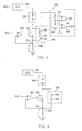
FIG. 1 is a circuit diagram of a conventional LED driving circuit;
FIG. 2 is a schematic diagram of a controller with protection function of the present invention;
FIG. 3 is a schematic diagram of an LED driving circuit with protection function according to a first embodiment of the present invention;
FIG. 4 is a schematic diagram of an LED driving circuit with protection function according to a second embodiment of the present invention;
FIG. 5 is a schematic diagram of an LED driving circuit with protection function according to a third embodiment of the present invention;
FIG. 6 is a schematic diagram of an LED driving circuit with protection function according to a forth embodiment of the present invention.
DETAILED DESCRIPTION
In the following detailed description, for purposes of explanation, numerous specific details are set forth in order to provide a thorough understanding of the disclosed embodiments. It will be apparent, however, that one or more embodiments may be practiced without these specific details. In other instances, well-known structures and devices are schematically shown in order to simplify the drawings.
FIG. 2 is a schematic diagram of a controller with protection function of the present invention. The controller comprises a transistor 230, a current control unit and a judgment unit 290, wherein the current control unit comprises an error amplifier 260 and a reference voltage generating unit 280. The transistor 230 may be built-in element or an external element. The transistor 230 has a control terminal, a first terminal and a second terminal. The first terminal of the transistor 230 is coupled to a terminal of a load 220 and a driving unit 210 is coupled to the other terminal of the load 220 to provide a driving voltage VDR to drive the load 220. A current detecting unit 240 is coupled to the second terminal of the transistor 230 to generate a current detecting signal Ifb. In the present embodiment, the current detecting unit 240 is a resistance. The error amplifier 260 receives the current detecting signal Ifb and a reference voltage Vref generated by the reference voltage generating unit 280 and controls an amount of a current flowing through the transistor 230 to be substantially stabilized at a preset current value. The judgment unit 290 comprises a first voltage divider element 292 coupled to the first terminal of the transistor 230 to generate a first voltage divider signal, and a comparison element 294. An inverting terminal of the comparison element 294 receives a first compared reference voltage Vr1 and a non-inverting terminal thereof receives the first voltage divider signal. Accordingly, a current reducing signal EN is generated when a level of the first voltage divider signal is higher than the first compared reference voltage Vr1.
The reference voltage generating unit 280 comprises a second voltage divider element 282, a switch element 284 and a voltage adjustment element 286. A terminal of the switch element 284 is coupled to the second voltage divider element 282 and the other terminal thereof is coupled to the voltage adjustment element 286. The voltage adjustment element 286 is a resistance in the present embodiment. The second voltage divider element 282 receives a base voltage Vr to generate a reference voltage Vref. The switch element 284 is turned on to change a voltage divider ratio of the second voltage divider element 282 to lower a level of the reference voltage Vref when the judgment unit 290 generates a current reducing signal EN. The error amplifier 260 controls the transistor 230 to make the level of the current detecting signal Ifb is equal to the level of the reference voltage Vref. When the potential of the first terminal of the transistor 230 is lower than a preset current reducing value (i.e., the level of the first voltage divider signal is lower than the level of the first compared reference voltage Vr1), the current flowing through the transistor 230 is substantially stabilized at a first current value. When the potential of the first terminal of the transistor 230 is higher than the preset current reducing value, the judgment unit 290 generates the current reducing signal EN to turn on the switch element 284 to make the level of the reference voltage Vref reduced. At this time, the error amplifier 260 controls the transistor 230 to reduce the current flowing through the transistor 230 until the level of the current detecting signal Ifb to be equal to the level of the reference voltage Vref after reduced. Then, the current flowing through the transistor 230 is substantially stabilized at a second current value.
By means of the error amplifier 260, the level of the current detecting signal Ifb is equal to the level of the reference voltage Vref and that is the level of the current detecting signal Ifb (i.e., the second terminal of the transistor 230) is a stable value. Therefore, the judgment unit 290 is coupled to the first terminal of the transistor 230 to judge a voltage difference between the first terminal and the second terminal of the transistor 230 by detecting the potential of the first terminal in the present embodiment. In actually, the judgment unit 290 may be coupled to the first and second terminals of the transistor 230 to directly determine whether generating the current reducing signal EN or not according to the voltage difference between the first and second terminals of the transistor 230, and so the controller of the present invention is applicable to any circuit systems.
FIG. 3 is a schematic diagram of an LED driving circuit with protection function according to a first embodiment of the present invention. The LED driving circuit comprises a driving unit 310, an LED module 320 and a controller, wherein the controller comprises a transistor 330, an error amplifier 360, a signal add unit 380 and a judgment unit 390. The transistor 330 is built-in internally in the controller in the present embodiment, and may be an external element in actual application. The driving unit 310 is coupled to a terminal of the LED module 320 to provide a driving voltage VDR to drive the LED module 320 for lighting. The transistor 330 has a control terminal, a first terminal coupled to the other terminal of the LED module 320 and a second terminal coupled to a current detecting unit 340. The current detecting unit 340 generates a current detecting signal Ifb according to an amount of a current flowing through the transistor 330. The judgment unit 390 comprises a first voltage divider element 392 and comparison elements 394, 396. The first voltage divider element 392 is coupled to the first terminal of the transistor 330 to generate a first voltage divider signal. An inverting terminal of the comparison element 394 receives a first compared reference voltage Vr1 and a non-inverting terminal thereof received the first voltage divider signal. An inverting terminal of the comparison element 396 receives a second compared reference voltage Vr2 and a non-inverting terminal thereof received the first voltage divider signal, wherein the level of the second compared reference voltage Vr2 is higher than the level of the first compared reference voltage Vr1. The voltage across the transistor 330 may be increased when a voltage across the LED module 320 is reduced due to that one or more LEDs are short-circuited. The comparison element 394 generates a current reducing signal EN when the level of the first voltage divider signal is higher than the level of the first compared reference voltage Vr1. Further, the comparison element 396 generates a protection signal PROT when the level of the first voltage divider signal is higher than the level of the second compared reference voltage Vr2.
The signal add unit 380 determines whether the level of the current detecting signal Ifb is increased a preset value or not according to the current reducing signal EN. The signal add unit 380 comprises a second voltage divider element 382, a switch element 384 and a signal adder 386. A terminal of the switch element 384 is coupled to the second voltage divider element 382 and the other terminal thereof is coupled to the signal adder 386. The second voltage divider 382 receives a reference voltage Vref to generate a second voltage divider signal. The switch element 384 determines whether the second voltage divider signal is transmitted to the signal adder 386 or not according to the current reducing signal EN. If the second voltage divider signal is transmitted to the signal adder 386, the level of the current detecting signal Ifb is increased according to the voltage divider signal. The error amplifier 360 receives a signal generated by the signal adder 386 and the reference voltage Vref and accordingly controls the amount of the current flowing through the transistor 330. A level of the signal generated by the signal add unit 380 is a sum of the second voltage divider signal and the current detecting signal Ifb when the current reducing signal EN generated. Therefore, the error amplifier 360 reduces the current flowing through the transistor 330 to be a second current value from a first current value and keeps the level of the signal generated by the signal add unit 380 being equal to the level of the reference voltage Vref.
Compared with the judgment unit 290 shown in the FIG. 2, the judgment unit 390 further comprises the comparison element 396. The comparison element 396 generates a protection signal PROT if the voltage of the first terminal of the transistor 330 is increased abnormally and even higher than a withstanding voltage of the transistor 330. In the present embodiment, the driving unit 310 can stop driving the LED module 320 to avoid damaging the transistor 330 according to the protection signal PROT.
FIG. 4 is a schematic diagram of an LED driving circuit with protection function according to a second embodiment of the present invention. The LED driving circuit comprises a driving unit 410, an LED module 420, a transistor 430 and a controller, wherein the controller comprises a select switch 484, an error amplifier 460 and a judgment unit 490. The driving unit 410 is coupled to a terminal of the LED module 420 to provide a driving voltage VDR to drive the LED module 420 for lighting. The transistor 430 has a control terminal, a first terminal and a second terminal. The first terminal of the transistor 430 is coupled to the other terminal of the LED module 420 and the second terminal thereof is coupled to a current detecting unit by the select element 484 to generate a current detecting signal Ifb, wherein the current detecting unit comprises a first current detecting resistance 440 and a second current detecting resistance 442. The select switch 484 is coupled to the transistor 430 and one of a first current detecting resistance 440 and the second current detecting resistance 442 in response to a current reducing signal EN. The judgment unit 490 comprises a first voltage divider element 492 and comparison elements 494, 496. The first voltage divider element 492 is coupled to a potential of the first terminal of the transistor 430 to generate a first voltage divider signal. An inverting terminal of the comparison element 494 receives a first compared reference voltage Vr1 and a non-inverting terminal thereof receives the first voltage divider signal. The comparison element 494 generates the current reducing signal EN when the level of the first voltage divider signal is higher than the level of the first compared reference voltage Vr1. An inverting terminal of the comparison element 496 receives a second compared reference voltage Vr2 and a non-inverting terminal thereof receives the first voltage divider signal. The comparison element 496 generates a protection signal PROT when the level of the first voltage divider signal is higher than the level of the second compared reference voltage Vr2, wherein the level of the second compared reference voltage Vr2 is higher than the level of the first compared reference voltage Vr1.
An inverting terminal of the error amplifier 460 receives the current detecting signal Ifb and a non-inverting terminal thereof receives a reference voltage Vref to accordingly output a control signal to the control terminal of the transistor 430, and so the level of the current detecting signal Ifb is equal to the level of the reference voltage Vref. In the present embodiment, the switch element 484 is coupled to the transistor 430 and the first current detecting resistance 440 when the current reducing signal EN is at low level (that is the level of the first voltage divider signal lower than the level of the first compared reference voltage Vr1). The error amplifier 460 substantially stabilizes the current flowing through the transistor 430 at a first current value. The switch element 484 is coupled to the transistor 430 and the second current detecting resistance 442 when the current reducing signal EN is at high level (that is the level of the first divided signal is higher than the level of the first compared reference voltage Vr1). The resistance value of the second current detecting resistance 442 is higher than the resistance value of the first current detecting resistance 440. Therefore, the error amplifier 460 substantially stabilizes the current flowing through the transistor 430 at a second current value, wherein the second current value is lower than the first current value.
The comparison element 496 is triggered to generate the protection signal PROT when the voltage of the first terminal of the transistor 430 is still increased due to abnormal conditions. The driving unit 410 stops driving the LED module 420 to avoid damaging the transistor 430 according to the protection signal PROT.
FIG. 5 is a schematic diagram of an LED driving circuit with protection function according to a third embodiment of the present invention. The LED driving circuit comprises a driving unit 510, an LED module 520 and a controller, wherein the controller comprises a transistor 530, an error amplifier 560, a current dividing unit 580 and a judgment unit 590. The driving unit 510 is coupled to a terminal of the LED module 520 to provide a driving voltage VDR to drive the LED module 520 for lighting. The transistor 530 has a control terminal, a first terminal coupled to the other terminal of the LED module 520 and a second terminal coupled to a current detecting unit 540. The current detecting unit 540 is a resistance and generates a current detecting signal Ifb according to an amount of a current flowing through the LED module 520. The error amplifier 560 controls the transistor 530 to substantially stabilize the current flowing through the LED module 520 (and the transistor 530) at a first current value according to the current detecting signal Ifb and a reference voltage Vref.
The judgment unit 590 comprises a first voltage divider element 592 and comparison elements 594, 596. The first voltage divider element 592 is coupled to the first terminal of the transistor 530 to generate a voltage divider signal. An inverting terminal of the comparison element 594 receives a first compared reference voltage Vr1 and a non-inverting terminal thereof receives the voltage divider signal. The comparison element 594 generates a current reducing signal EN when the level of the voltage divider signal is higher than the level of the first compared reference voltage Vr1. An inverting terminal of the comparison element 596 receives a second compared reference voltage Vr2 and a non-inverting terminal thereof receives the voltage divider signal. The comparison element 596 generates a protection signal PROT when the level of the voltage divider signal is higher than the level of the second compared reference voltage Vr2, wherein the level of the second compared reference voltage Vr2 is higher than the level of the first compared reference voltage Vr1. The current dividing unit 580 is coupled to the first and second terminals of the transistor 530 and determines whether dividing the current of the transistor 530 or not according to the current reducing signal EN. In the present embodiment, the current dividing unit 580 comprises a current dividing resistance 582 and a switch element 584 connected in series. The switch element 584 is turned on to make a part of current flowing through the LED module 520 to flow through the current dividing unit 580 when the current reducing signal EN is generated by the judgment unit 590. Therefore, the amount of the current flowing through the transistor 530 can be reduced. The comparison element 596 is triggered to generate the protection signal PROT when the voltage of the first terminal of the transistor 530 is increased abnormally. The driving unit 510 stops driving the LED module 520 to avoid the voltage of the first terminal of the transistor 530 exceeding a withstanding voltage of the transistor 530 according to the protection signal PROT.
FIG. 6 is a schematic diagram of an LED driving circuit with protection function according to a forth embodiment of the present invention. The LED driving circuit comprises a driving unit 610, an LED module 620 and a controller, wherein the controller comprises a transistor 630, an error amplifier 660 and a current dividing unit 680. The driving unit 610 is coupled to a terminal of the LED module 620 to provide a driving voltage VDR to drive the LED module 620 for lighting. The transistor 630 has a control terminal, a first terminal coupled to the other terminal of the LED module 620 and a second terminal coupled to a current detecting unit 640. The current detecting unit 640 is a resistance and generates a current detecting signal Ifb according to an amount of a current flowing through the LED module 620. The error amplifier 660 controls the transistor 630 to substantially stabilize the current flowing through the LED module 620 to at a first current value according to the current detecting signal Ifb and a reference voltage Vref.
The current dividing unit 680 is connected with the transistor 630 in parallel and comprises a current dividing resistance 682 and a zener diode 686 connected in series. The current dividing unit 680 divides the current of the transistor 630 by the current dividing resistance 682 and the zener diode 686 when a voltage across the transistor 630 is higher than a preset value (that is a voltage across the transistor 630 is higher than a breakdown voltage of the zener diode 686.
All the features disclosed in this specification (including any accompanying claims, abstract, and drawings) may be replaced by alternative features serving the same, equivalent or similar purpose, unless expressly stated otherwise. Thus, unless expressly stated otherwise, each feature disclosed is one example only of a generic series of equivalent or similar features.

Claims (6)

What is claimed is:
1. A controller with protection function, used to control a transistor having a control terminal, a first terminal coupled to a load and a second terminal, comprising:
a judgment unit, coupled to the transistor and generating a current reducing signal when a potential of the first terminal of the transistor or the voltage difference between the first terminal and the second terminal of the transistor is higher than a first preset value; and
a current control unit, coupled to the control terminal of the transistor to control a current flowing through the transistor to substantially be a preset current value and reducing the current when receiving the current reducing signal,
wherein the second terminal of the transistor is coupled to a current detecting unit which generates a current detecting signal according to an amount of a current flowing through the current detecting unit and controls the current flowing through the transistor according to the current detecting signal, the current detecting unit comprises a first current detecting resistance and a second current detecting resistance and the current control unit comprises a select switch, and an end of the select switch is coupled to the second terminal of the transistor and the other end thereof is coupled to the first current detecting resistance or the second current detecting resistance according to the current reducing signal.
2. The controller with protection function according to claim 1, wherein the judgment unit comprises a first voltage divider element coupled to the first terminal of the transistor and a comparison element coupled to the first voltage divider element, and the comparison element generates the current reducing signal according to the potential of the first terminal of the transistor and a first compared reference voltage.
3. The controller with protection function according to claim 1, wherein the judgment unit further generates a protection signal when the potential of the first terminal of the transistor or the voltage difference between the first terminal and the second terminal of the transistor is higher than a second preset value, in which the second preset value is higher than the first preset value.
4. A controller with protection function, used to control a transistor having a control terminal, a first terminal coupled to a load and a second terminal, comprising:
a judgment unit, coupled to the transistor and generating a current reducing signal when a potential of the first terminal of the transistor or the voltage difference between the first terminal and the second terminal of the transistor is higher than a first preset value; and
a current control unit, coupled to the control terminal of the transistor to control a current flowing through the transistor to substantially be a preset current value and reducing the current when receiving the current reducing signal, the current control unit further comprises a reference voltage generating unit which is used to generate a reference voltage, the current control unit adjusts the amount of the current flowing through the transistor according to the level of the reference voltage and the reference voltage generating unit reduces a level of the reference voltage when receiving the current reducing signal,
wherein the reference voltage generating unit comprises a second voltage divider element, a switch element, and a voltage adjustment element, and the second voltage divider element receives a base voltage to generate a reference voltage, in which a terminal of the switch element is coupled to the second voltage divider element and another terminal thereof is coupled or de-coupled to the voltage adjustment element according to the current reducing signal to adjust the level of the reference voltage.
5. The controller with protection function according to claim 4, wherein the judgment unit further generates a protection signal when the potential of the first terminal of the transistor or the voltage difference between the first terminal and the second terminal of the transistor is higher than a second preset value, in which the second preset value is higher than the first preset value.
6. A controller with protection function, used to control a transistor having a control terminal, a first terminal coupled to a load and a second terminal, comprising:
a judgment unit, coupled to the transistor and generating a current reducing signal when a potential of the first terminal of the transistor or the voltage difference between the first terminal and the second terminal of the transistor is higher than a first preset value; and
a current control unit, coupled to the control terminal of the transistor to control a current flowing through the transistor to substantially be a preset current value and reducing the current when receiving the current reducing signal,
wherein the second terminal of the transistor is coupled to a current detecting unit which generates a current detecting signal according to an amount of a current flowing through the current detecting unit and controls the current flowing through the transistor according to the current detecting signal, the current control unit further comprises a signal add unit which is coupled to the current detecting unit and increases the level of the current detecting signal at a preset value in response to the current reducing signal.
US13/354,295 2011-03-22 2012-01-19 Controller and LED driving circuit with protection function Active 2032-07-20 US8872441B2 (en)

Applications Claiming Priority (3)

Application Number Priority Date Filing Date Title
TW100109786A TWI547197B (en) 2011-03-22 2011-03-22 Controller and led driving circuit with current limiting function
TW100109786 2011-03-22
TW100109786A 2011-03-22

Publications (2)

Publication Number Publication Date
US20120242249A1 US20120242249A1 (en) 2012-09-27
US8872441B2 true US8872441B2 (en) 2014-10-28

Family

ID=46860564

Family Applications (1)

Application Number Title Priority Date Filing Date
US13/354,295 Active 2032-07-20 US8872441B2 (en) 2011-03-22 2012-01-19 Controller and LED driving circuit with protection function

Country Status (3)

Country Link
US (1) US8872441B2 (en)
CN (1) CN102695326B (en)
TW (1) TWI547197B (en)

Families Citing this family (9)

* Cited by examiner, † Cited by third party
Publication number Priority date Publication date Assignee Title
TWI459855B (en) * 2012-10-19 2014-11-01 Raydium Semiconductor Corp Led driving apparatus having holding current circuit and operating method thereof
CN103491666B (en) * 2012-12-19 2015-07-29 深圳市安派电子有限公司 A kind of flasher of power valve protective circuit
CN104427680B (en) * 2013-08-22 2017-04-12 瑞昱半导体股份有限公司 Protective circuit used for control integrated circuit of light emitting diodes
CN104679089B (en) * 2013-11-26 2016-03-09 上海贝岭股份有限公司 Step excess temperature for integrated LED driving chip compensates protection system and circuit
JP6211554B2 (en) 2015-04-15 2017-10-11 株式会社東海理化電機製作所 LED driving device
DE102018108910B3 (en) * 2018-04-16 2019-07-04 Elmos Semiconductor Aktiengesellschaft Light source for short LED light pulses and method for generating light pulses
CN111198470B (en) * 2018-10-30 2022-03-18 中强光电股份有限公司 Projection system, driving device and driving method
CN111983271A (en) * 2019-05-21 2020-11-24 上海海拉电子有限公司 Protection circuit for high-voltage insulation test
CN111586929A (en) * 2020-05-28 2020-08-25 成都航天凯特机电科技有限公司 Infrared light filling lamp circuit of VCSEL without red explosion

Citations (11)

* Cited by examiner, † Cited by third party
Publication number Priority date Publication date Assignee Title
US20020050853A1 (en) * 2000-10-27 2002-05-02 Mitsuru Hosoki Stabilized power circuit
US6424131B1 (en) * 1999-06-18 2002-07-23 Matsushita Electric Industrial Co., Ltd. Output controller
US20020171455A1 (en) * 2001-05-17 2002-11-21 Masahiro Tsuchida Electric load drive apparatus
US6496168B1 (en) * 1999-10-04 2002-12-17 Autonetworks Technologies, Ltd. Display element drive device
US20050162216A1 (en) * 2004-01-27 2005-07-28 Denso Corporation Semiconductor integrated circuit device
CN101103468A (en) 2005-01-13 2008-01-09 松下电器产业株式会社 Semiconductor device for driving LED, and led driving device
US20080315773A1 (en) 2007-06-21 2008-12-25 Sung-Man Pang Light emitting diode driving circuit
US20090058313A1 (en) * 2007-08-30 2009-03-05 Shih-Hsien Chang Power supply for supplying power to a lamp
CN201307951Y (en) 2008-11-12 2009-09-09 登丰微电子股份有限公司 Light-emitting diode drive circuit
CN101902855A (en) 2009-05-27 2010-12-01 登丰微电子股份有限公司 LED driving circuit and backlight module
US8049690B2 (en) * 2008-02-19 2011-11-01 Himax Analogic, Inc. Circuit and method for driving light emitting diodes

Patent Citations (11)

* Cited by examiner, † Cited by third party
Publication number Priority date Publication date Assignee Title
US6424131B1 (en) * 1999-06-18 2002-07-23 Matsushita Electric Industrial Co., Ltd. Output controller
US6496168B1 (en) * 1999-10-04 2002-12-17 Autonetworks Technologies, Ltd. Display element drive device
US20020050853A1 (en) * 2000-10-27 2002-05-02 Mitsuru Hosoki Stabilized power circuit
US20020171455A1 (en) * 2001-05-17 2002-11-21 Masahiro Tsuchida Electric load drive apparatus
US20050162216A1 (en) * 2004-01-27 2005-07-28 Denso Corporation Semiconductor integrated circuit device
CN101103468A (en) 2005-01-13 2008-01-09 松下电器产业株式会社 Semiconductor device for driving LED, and led driving device
US20080315773A1 (en) 2007-06-21 2008-12-25 Sung-Man Pang Light emitting diode driving circuit
US20090058313A1 (en) * 2007-08-30 2009-03-05 Shih-Hsien Chang Power supply for supplying power to a lamp
US8049690B2 (en) * 2008-02-19 2011-11-01 Himax Analogic, Inc. Circuit and method for driving light emitting diodes
CN201307951Y (en) 2008-11-12 2009-09-09 登丰微电子股份有限公司 Light-emitting diode drive circuit
CN101902855A (en) 2009-05-27 2010-12-01 登丰微电子股份有限公司 LED driving circuit and backlight module

Non-Patent Citations (2)

* Cited by examiner, † Cited by third party
Title
"First Office Action of China Counterpart Application", issued on Dec. 3, 2013, p. 1-p. 10, in which the listed references were cited.
"First Office Action of Taiwan Counterpart Application", issued on Apr. 14, 2014, p. 1-p. 7, in which the listed reference was cited.

Also Published As

Publication number Publication date
US20120242249A1 (en) 2012-09-27
TW201240513A (en) 2012-10-01
CN102695326B (en) 2015-04-01
CN102695326A (en) 2012-09-26
TWI547197B (en) 2016-08-21

Similar Documents

Publication Publication Date Title
US8872441B2 (en) Controller and LED driving circuit with protection function
US8687332B2 (en) Transistor circuit with protecting function
US8928231B2 (en) Open LED detection and recovery system for LED lighting system
US20160192456A1 (en) Driving circuits and methods for controlling light source
US8742692B2 (en) LED driving circuit and short-circuit protection circuit
US20120274235A1 (en) Power Converting Circuit and Converting Controller
US8248045B2 (en) Charge pump circuit with current detecting and method thereof
KR102051694B1 (en) Leakage currrent detection circuit, light apparatus comprising the same and leakage currrent detection method
US9107271B2 (en) LED driving circuit
JP2008197892A (en) Series regulator
US20150207307A1 (en) Boost apparatus with over-current and over-voltage protection function
US9246323B2 (en) Current controller and protection circuit
US20140169050A1 (en) Blanking control circuit for controlling synchronous rectifier and method of controlling synchronous rectifier using the circuit
JP2010110091A (en) Load driving device
US9343901B2 (en) Power system and short-circuit protection circuit thereof
US9240716B2 (en) Switching power supply circuit
KR20170123274A (en) Dc-dc converter
US8638050B2 (en) DC power supply unit and LED lighting apparatus
JP4509731B2 (en) Lighting control circuit for vehicular lamp
US8492993B2 (en) LED driving circuit and power converting circuit
US10440797B2 (en) Lighting device and illuminating fixture
KR20130056085A (en) Short protection circuit of led lighting part
US11272591B1 (en) Constant power light emitting diode (LED) driver
US20130271006A1 (en) LED Driving Circuit
TW201521512A (en) LED driving circuit

Legal Events

Date Code Title Description
AS Assignment

Owner name: GREEN SOLUTION TECHNOLOGY CO., LTD., TAIWAN

Free format text: ASSIGNMENT OF ASSIGNORS INTEREST;ASSIGNORS:YU, CHUNG-CHE;LEE, LI-MIN;SHIU, SHIAN-SUNG;REEL/FRAME:027638/0263

Effective date: 20120118

STCF Information on status: patent grant

Free format text: PATENTED CASE

MAFP Maintenance fee payment

Free format text: PAYMENT OF MAINTENANCE FEE, 4TH YR, SMALL ENTITY (ORIGINAL EVENT CODE: M2551)

Year of fee payment: 4

MAFP Maintenance fee payment

Free format text: PAYMENT OF MAINTENANCE FEE, 8TH YR, SMALL ENTITY (ORIGINAL EVENT CODE: M2552); ENTITY STATUS OF PATENT OWNER: SMALL ENTITY

Year of fee payment: 8