US8871649B2 - Methods of forming trench/hole type features in a layer of material of an integrated circuit product - Google Patents
Methods of forming trench/hole type features in a layer of material of an integrated circuit product Download PDFInfo
- Publication number
- US8871649B2 US8871649B2 US13/834,946 US201313834946A US8871649B2 US 8871649 B2 US8871649 B2 US 8871649B2 US 201313834946 A US201313834946 A US 201313834946A US 8871649 B2 US8871649 B2 US 8871649B2
- Authority
- US
- United States
- Prior art keywords
- layer
- insulating material
- photoresist
- forming
- opening
- Prior art date
- Legal status (The legal status is an assumption and is not a legal conclusion. Google has not performed a legal analysis and makes no representation as to the accuracy of the status listed.)
- Expired - Fee Related
Links
Images


Classifications
-
- H—ELECTRICITY
- H01—ELECTRIC ELEMENTS
- H01L—SEMICONDUCTOR DEVICES NOT COVERED BY CLASS H10
- H01L21/00—Processes or apparatus adapted for the manufacture or treatment of semiconductor or solid state devices or of parts thereof
- H01L21/70—Manufacture or treatment of devices consisting of a plurality of solid state components formed in or on a common substrate or of parts thereof; Manufacture of integrated circuit devices or of parts thereof
- H01L21/71—Manufacture of specific parts of devices defined in group H01L21/70
- H01L21/768—Applying interconnections to be used for carrying current between separate components within a device comprising conductors and dielectrics
- H01L21/76801—Applying interconnections to be used for carrying current between separate components within a device comprising conductors and dielectrics characterised by the formation and the after-treatment of the dielectrics, e.g. smoothing
- H01L21/76802—Applying interconnections to be used for carrying current between separate components within a device comprising conductors and dielectrics characterised by the formation and the after-treatment of the dielectrics, e.g. smoothing by forming openings in dielectrics
- H01L21/76816—Aspects relating to the layout of the pattern or to the size of vias or trenches
-
- H—ELECTRICITY
- H01—ELECTRIC ELEMENTS
- H01L—SEMICONDUCTOR DEVICES NOT COVERED BY CLASS H10
- H01L21/00—Processes or apparatus adapted for the manufacture or treatment of semiconductor or solid state devices or of parts thereof
- H01L21/70—Manufacture or treatment of devices consisting of a plurality of solid state components formed in or on a common substrate or of parts thereof; Manufacture of integrated circuit devices or of parts thereof
- H01L21/71—Manufacture of specific parts of devices defined in group H01L21/70
- H01L21/768—Applying interconnections to be used for carrying current between separate components within a device comprising conductors and dielectrics
- H01L21/76801—Applying interconnections to be used for carrying current between separate components within a device comprising conductors and dielectrics characterised by the formation and the after-treatment of the dielectrics, e.g. smoothing
- H01L21/76802—Applying interconnections to be used for carrying current between separate components within a device comprising conductors and dielectrics characterised by the formation and the after-treatment of the dielectrics, e.g. smoothing by forming openings in dielectrics
- H01L21/76804—Applying interconnections to be used for carrying current between separate components within a device comprising conductors and dielectrics characterised by the formation and the after-treatment of the dielectrics, e.g. smoothing by forming openings in dielectrics by forming tapered via holes
-
- H—ELECTRICITY
- H01—ELECTRIC ELEMENTS
- H01L—SEMICONDUCTOR DEVICES NOT COVERED BY CLASS H10
- H01L21/00—Processes or apparatus adapted for the manufacture or treatment of semiconductor or solid state devices or of parts thereof
- H01L21/02—Manufacture or treatment of semiconductor devices or of parts thereof
- H01L21/027—Making masks on semiconductor bodies for further photolithographic processing not provided for in group H01L21/18 or H01L21/34
- H01L21/033—Making masks on semiconductor bodies for further photolithographic processing not provided for in group H01L21/18 or H01L21/34 comprising inorganic layers
- H01L21/0334—Making masks on semiconductor bodies for further photolithographic processing not provided for in group H01L21/18 or H01L21/34 comprising inorganic layers characterised by their size, orientation, disposition, behaviour, shape, in horizontal or vertical plane
- H01L21/0337—Making masks on semiconductor bodies for further photolithographic processing not provided for in group H01L21/18 or H01L21/34 comprising inorganic layers characterised by their size, orientation, disposition, behaviour, shape, in horizontal or vertical plane characterised by the process involved to create the mask, e.g. lift-off masks, sidewalls, or to modify the mask, e.g. pre-treatment, post-treatment
-
- H—ELECTRICITY
- H01—ELECTRIC ELEMENTS
- H01L—SEMICONDUCTOR DEVICES NOT COVERED BY CLASS H10
- H01L21/00—Processes or apparatus adapted for the manufacture or treatment of semiconductor or solid state devices or of parts thereof
- H01L21/02—Manufacture or treatment of semiconductor devices or of parts thereof
- H01L21/04—Manufacture or treatment of semiconductor devices or of parts thereof the devices having at least one potential-jump barrier or surface barrier, e.g. PN junction, depletion layer or carrier concentration layer
- H01L21/18—Manufacture or treatment of semiconductor devices or of parts thereof the devices having at least one potential-jump barrier or surface barrier, e.g. PN junction, depletion layer or carrier concentration layer the devices having semiconductor bodies comprising elements of Group IV of the Periodic System or AIIIBV compounds with or without impurities, e.g. doping materials
- H01L21/30—Treatment of semiconductor bodies using processes or apparatus not provided for in groups H01L21/20 - H01L21/26
- H01L21/31—Treatment of semiconductor bodies using processes or apparatus not provided for in groups H01L21/20 - H01L21/26 to form insulating layers thereon, e.g. for masking or by using photolithographic techniques; After treatment of these layers; Selection of materials for these layers
- H01L21/3105—After-treatment
- H01L21/311—Etching the insulating layers by chemical or physical means
- H01L21/31144—Etching the insulating layers by chemical or physical means using masks
Definitions
- the present disclosure relates to the manufacture of sophisticated semiconductor devices, and, more specifically, to various novel methods of forming trench/hole type features in a layer of material of an integrated circuit product.
- MOSFETs Metal oxide field effect transistors
- a FET is a device that typically includes a source region, a drain region, a channel region that separates the source region and the drain region, and a gate electrode positioned above the channel region.
- a gate insulation layer is positioned between the gate electrode and the channel region that will be formed in the substrate.
- FETs have been substantially planar devices, but similar principles of operation apply to more three-dimensional FET structures, devices that are typically referred to as FinFETs.
- a typical integrated circuit product also includes many levels, e.g., 7-10, of so-called metallization layers that constitute the electrical “wiring” that provides a means to electrically connect to the integrated circuits formed in the semiconducting substrate.
- the metallization layers comprise layers of insulating materials having various conductive structures, e.g., conductive lines and vias, formed therein.
- the conductive vias provide electrical connection between an underlying conductive line in an underlying metallization layer and an overlying conductive line in an overlying metallization layer.
- the conductive lines and vias are typically formed using single-damascene or dual-damascene techniques, although such conductive structures may sometimes be formed using traditional deposition/photolithography/patterning techniques.
- improving the functionality and performance capability of various metallization systems has become important in designing modern semiconductor devices.
- One example of such improvements is the enhanced use of copper metallization systems in integrated circuit devices and the use of so-called “low-k” or ULK dielectric materials (for example, materials having a dielectric constant less than 3) in such devices.
- Copper metallization systems exhibit improved electrical conductivity as compared to, for example, prior art metallization systems using aluminum for the conductive lines and vias.
- the use of low-k dielectric materials also tends to improve the signal-to-noise ratio (S/N ratio) by reducing crosstalk as compared to other dielectric materials with higher dielectric constants.
- this increased overall “crowding” of the various conductive lines and vias means that device designers have had to become very creative in terms of minimizing the physical size of such conductive lines and vias and in providing means to insure proper alignment between adjacent levels of such conductive structures when alignment tolerances or “process windows” are very small.
- formation of a conductive line or via in a layer of insulating material involves forming a trench-type or hole-type feature, respectively, in a layer of insulating material.
- the process of forming a conductive line/via generally involves depositing a layer of insulating material, forming a patterned etch mask comprised of a photoresist material above the layer of insulating material, performing an etching process through the etch mask to define the trench/hole type feature in the layer of insulating material, removing the patterned etch mask, overfilling the trench/hole type feature with a conductive material, such as copper, and removing excess portions of the conductive material positioned outside of the trench/hole type feature by performing a chemical mechanical planarization (CMP) process.
- CMP chemical mechanical planarization
- photolithography tools and systems typically include a source of radiation at a desired wavelength, an optical system and, typically, the use of a so-called mask or reticle that contains a pattern that is desired to be formed on a wafer.
- Radiation is provided through or reflected off the mask or reticle to form an image on a light-sensitive layer of photoresist material that is formed above a semiconductor wafer.
- the radiation used in such systems may be light, such as ultraviolet light, deep ultraviolet light (DUV), vacuum ultraviolet light (VUV), extreme ultraviolet light (EUV), etc.
- the radiation may also be x-ray radiation, e-beam radiation, etc.
- a patterned photoresist mask layer is formed that may be used for a variety of purposes, e.g., as an etch mask to form trench/hole type features in an underlying layer of insulating material.
- DUV deep ultraviolet systems
- a typical photolithography process generally involves the steps of: (1) applying a layer of photoresist above a wafer or substrate, typically accomplished by a spin-coating process; (2) pre-baking (or soft-baking) the layer of photoresist at a temperature of approximately 90-120° C. to reduce the level of solvents in the layer of photoresist and to improve the adhesion characteristics of the photoresist; (3) performing an exposure process, wherein a pattern on a reticle is projected onto the layer of photoresist used in a stepper tool to create a latent image in the layer of photoresist; (4) performing a post-exposure bake on the layer of photoresist at a temperature approximately 5-15° C.
- the trench/hole type feature has a target critical dimension (CD) or width that the process engineer tries to achieve based on the design criteria and rules for the particular product under design.
- CD critical dimension
- trench/hole type features were larger in size, they were formed in a layer of insulating material by forming a post-litho etch mask that had openings that corresponded to the trench/hole type features that were to be directly etched into the underlying layer of insulating material.
- a positive etch bias etch process is one whereby the etched feature has a larger dimension than that of the corresponding feature defined in the patterned layer of photoresist. For example, a square opening in a patterned layer of photoresist may have a critical dimension of 40 nm.
- the contact opening will have a larger critical dimension, e.g., 50 nm, than that of the opening in the patterned layer of photoresist.
- NTD negative tone developer
- etch bias etching process to produce the required smaller features.
- this process involves forming a patterned layer of photoresist where the post-litho openings are as close as possible to the final desired target dimension for the feature. This required pushing the photolithography equipment to its limits to produce a patterned layer of photoresist with such very small sized post-litho openings.
- the NTD process involved use of a clear-tone reticle (a “clear-field” mask) with a dark-field line that corresponds to the trench/hole type feature to expose the layer of photoresist.
- a clear-tone reticle a “clear-field” mask
- the exposed photoresist material is left in place while the non-exposed material is removed.
- a negative etch bias etch process was performed to define the trench/hole type feature in the underlying layer of material, wherein the feature exhibited inwardly tapered sidewalls.
- a negative etch bias etch process is one whereby the etched feature has a smaller dimension than that of the corresponding feature defined in the patterned layer of photoresist.
- a square opening in a patterned layer of photoresist may have a critical dimension of 40 nm.
- the contact opening will have a smaller critical dimension, e.g., 30 nm, than that of the opening in the patterned layer of photoresist.
- the negative etch bias process was performed as a means to effectively reduce the critical dimension of the resulting conductive line/via beyond what could be directly patterned using the previous PTD/positive etch bias processing techniques described above.
- FIG. 1 depicts a prior art formation process for two illustrative trench/hole type features 10 A/ 10 B and will be referenced to further explain some of the problems associated with existing prior art methodologies.
- FIG. 1 depicts the features at three points during the fabrication process: (1) as-drawn target during the design process; (2) the post-lithography condition after a patterned photoresist mask has been formed based upon the as-drawn target; and (3) the post-etch condition.
- the upper portion of FIG. 1 depicts the tip-to-tip spacing between the features, whereas the lower portion of FIG. 1 depicts the tip-to-side spacing between the features.
- the dimensions of the feature changes during the course of the lithography and etching processes and the spacing between the features changes accordingly.
- the features have a target length 12 T, a post-litho length 12 PL and a post-etch length 12 PE, wherein the post-litho length 12 PL is greater than the target length 12 T, and the post-etch length 12 PE is less than the target length 12 T.
- the features have a target width 14 T, and a post-litho width 14 PL that is greater than the target width 14 T.
- the post-etch width 14 PE is equal to the target width 14 T.
- the target dimensions of the features are drawn as precisely as the photolithography systems and materials will allow. However, as indicated in FIG.
- the overall size of the feature, post-lithography tends to be larger than its target dimensions, e.g., the post-lithography length 12 PL and width 14 PL are larger than the target length 12 T and target width 14 T, respectively.
- the post-etch feature tends to be smaller in physical size than the post-litho feature, i.e., the post-etch length 12 PE and width 14 PE are less than post-litho length 12 PL and width 14 PL, respectively.
- the reduction in size of the features from the post-litho size to the post-etch size enables the desired reduction in feature size in terms of the width or critical dimension of the trench/hole type features which is necessary in manufacturing modern integrated circuit products.
- the magnitude of dimensional changes in the features is different in the length direction as compared to the width direction of the feature. More specifically, there is a length or tip etch bias 18 and a width or side etch bias 20 .
- the tip-to-tip spacing for the target condition 16 T, the post-litho condition 16 PL and the post-etch condition 16 PE are depicted.
- the post-litho spacing 16 PL is less than the target spacing 16 T and the post-etch spacing 16 PE is even less than the target spacing 16 T.
- post-litho width 14 PL is greater than the target width 14 T or the post-etch width 14 PE.
- the post-litho spacing 16 PL may be 50 nm, while the post-etch spacing 16 PE may be 80 nm which equates to a tip etch bias 18 of 15 nm.
- post-litho width 14 PL may be about 40 nm, while the post-etch width 14 PE may be about 20 nm, which equates to a side etch bias 20 of 10 nm.
- line-end-pull-back This overall change in the feature size from post-lithography to post-etch is sometimes referred to as “line-end-pull-back,” which is typically described by a ratio between the tip etch bias 18 and the side etch bias 20 .
- the line-end-pull-back would be about 1.5 (15/10).
- the post-etch tip-to-side spacing 15 PE is greater than the post-litho tip-to-side spacing 17 PL due to this line-end-pull-back issue.
- the tip etch bias 18 is greater than the side etch bias 20 , which can have adverse effects on tip-to-tip and tip-to-side spacing between features because of the increased loss in the length direction when forming trench/hole type features as described above.
- FIG. 2 depicts situations wherein the above-described difference in etch bias may have adverse impacts as it relates to forming conductive lines and vias on integrated circuit products.
- FIG. 2 depicts three situations (“short,” “target” and “open”) for the connection between where conductive line features 30 A, 30 B are formed in a first layer of insulating material and a conductive line feature 32 formed in an overlying layer of insulating material.
- the tip-to-tip spacing 30 S between the conductive line features 30 A, 30 B will be large enough such that the overlying conductive line 32 will only be conductively coupled to the feature 30 A and it will not be conductively coupled to the feature 30 B. If the tip-to-tip spacing between the features 30 A, 30 B becomes smaller than the target spacing 30 S, then a short circuit will occur as the features 30 A, 30 B will contact one another, as indicated at the arrow 34 , and the line 32 is conductively coupled to the feature 30 B. Conversely, if the tip-to-tip spacing becomes wider than the target spacing 30 S, an open circuit will result as the line 32 is not conductively coupled to the feature 30 A.
- Negative etch biasing also has the undesirable effect of creating trench/hole type features with inwardly sloped sidewalls, i.e., the width at the top of the trench/hole type feature is greater than width at the bottom of the trench/hole type feature.
- the key metric for tip-to-tip spacing for trench/hole type features is the critical dimension at the bottom of the opening (because it is the bottom of the feature that makes contact with an underlying feature in an underlying metallization layer), which becomes larger post-etch than it is post-litho.
- the reduction in feature size can undesirably increase spacing between adjacent structures, e.g., it can increase tip-to-tip and tip-to-side spacing, which may lead to some of the problems identified above.
- the cross-sectional configuration of the trench/hole type feature would be approximately rectangular or square with substantially vertically oriented sidewalls.
- the present disclosure is directed to various novel methods of forming trench/hole type features in a layer of material of an integrated circuit product that may solve or reduce one or more of the problems identified above.
- the present disclosure is directed to various novel methods of forming trench/hole type features in a layer of material of an integrated circuit product.
- One illustrative method disclosed herein involves forming a layer of insulating material, forming a patterned layer of photoresist above the layer of insulating material, wherein the patterned layer of photoresist has an opening defined therein, forming an internal spacer within the opening in the patterned layer of photoresist, wherein the spacer defines a reduced-size opening, performing an etching process through the reduced-size opening on the layer of insulating material to define a trench/hole type feature in the layer of insulating material, and forming a conductive structure in the trench/hole type feature in the layer of insulating material.
- Another illustrative method disclosed herein involves forming a layer of photoresist above a layer of insulating material, exposing the layer of photoresist material, developing the exposed layer of photoresist material using a positive tone developer, wherein the patterned layer of photoresist has an opening defined therein, forming an internal spacer within the opening in the patterned layer of photoresist, wherein the spacer defines a reduced-size opening, performing a positive etch bias etching process through the reduced-size opening on the layer of insulating material to define a trench/hole type feature in the layer of insulating material, and forming a conductive structure in the trench/hole type feature in the layer of insulating material.
- the present disclosure is directed to various novel methods of forming trench/hole type features in a layer of material of an integrated circuit product.
- the methods disclosed herein may be employed in manufacturing a variety of different devices, including, but not limited to, logic devices, memory devices, etc., and they may be employed with respect to a variety of different technologies, e.g., N-type devices, P-type devices, CMOS applications, etc.
- N-type devices e.g., N-type devices, P-type devices, CMOS applications, etc.
- FIG. 3A is a drawing that, at a high level, depicts at least some aspects of the novel methods disclosed herein for forming trench/hole type features in a layer of material.
- the methods disclosed herein involve, after the patterned photoresist etch mask is formed, i.e., after the post-litho mask is formed, the processes disclosed herein involve performing one or both of a post-litho conformal shrink process and a positive bias etching process on the underlying layer of material to define the trench/hole type feature.
- the discussion below will make reference to several points in the process flow of forming a conductive line/via type feature in such a trench/hole type feature. More specifically, as shown in FIG.
- the following discussion will involve reference to: (1) the condition corresponding to the as-drawn target for the trench/hole type feature; (2) the post-lithography condition after a patterned photoresist mask has been formed based upon the as-drawn target; (3) the condition after the conformal shrink process has been performed on the post-lithography patterned photoresist mask; and (4) the post-etch condition using an illustrative positive etch bias etching process.
- FIG. 3B is a simplified view of a portion of an illustrative integrated circuit product 100 at an intermediate stage of manufacturing that is formed above a semiconducting substrate (not shown).
- the product 100 may be any type of integrated circuit product that employs any type of integrated circuit and any of a variety of different shaped conductive structures, e.g., conductive lines and vias, that are formed in various metallization layers commonly found on integrated circuit products.
- conductive lines and vias e.g., conductive lines and vias
- a conductive feature 102 has been formed in a layer of insulating material 101
- a second layer of insulating material 103 has been formed above the layer of insulating material 101
- a patterned layer of photoresist material 104 having a trench/line type opening 104 A formed therein, has been formed above the layer of insulating material 103 .
- the inventions disclosed herein may be employed in forming trench/hole type features and corresponding conductive lines and vias having any desired shape, depth or configuration.
- the trench/hole type features and corresponding conductive lines and vias discussed herein are intended to be representative of any type of opening in any type of material wherein a conductive structure may be formed.
- the conductive feature 102 is a substantially rectangular post-type conductive via.
- the various components and structures of the product 100 may be initially formed using a variety of different materials and by performing a variety of known techniques.
- the layers of insulating material 101 , 103 may be comprised of any type of insulating material, e.g., silicon dioxide, a low-k insulating material (k value less than 3), a high-k material (k value greater than 10), etc., they may be formed to any desired thickness, and they may be formed by performing a variety of known techniques, for example, a chemical vapor deposition (CVD) process, an atomic layer deposition (ALD) process, plasma-enhanced versions of those processes, or a spin-on deposition (SOD) process, etc.
- CVD chemical vapor deposition
- ALD atomic layer deposition
- SOD spin-on deposition
- the layer of insulating material 103 was deposited above the layer of insulating material 101 using traditional deposition techniques. Thereafter, the patterned layer of photoresist material 104 was formed above the layer of insulating material 103 using the photolithography processes described above.
- the target dimensions (length and width) of the opening 104 A may be at or near the limits of resolution of the photolithographic equipment, as was described in connection with the formation of trench/hole type features using the prior art methodologies discussed in the background section of this application. In other embodiments, the target dimensions for the opening 104 A may be more “relaxed” and not at the capability limits of the photolithographic equipment and technology.
- the attached drawings are not to scale, in the depicted example, the opening 104 A has a width that is larger than the width of the underlying conductive feature 102 .
- FIG. 3C depicts the product 100 after a layer of spacer material 105 has been deposited across the product and in the trench/hole type feature opening 104 A using a conformal deposition process.
- the layer of spacer material 105 may be made of a variety of different materials, its thickness may vary depending upon the particular application and it may be initially deposited by a variety of techniques.
- the layer of spacer material 105 may be comprised of any type of spacer material, silicon dioxide, carbon-containing materials, silicon nitride, amorphous carbon, a material that may be manufactured using a DSA process, etc., its thickness may fall within the range of about 1-50 nm (depending upon the application) and it may be formed by conformal processes such as ALD, CVD, DSA (directed self-assembly), etc.
- FIG. 3D depicts the product 100 after an anisotropic etching process has been performed on the layer of spacer material 105 to thereby define an internal spacer 105 A within the opening 104 A.
- the etch process selectively etches the layer of spacer material 105 relative to the layer of insulating material 103 and the patterned layer of photoresist material 104 .
- the internal spacer 105 A may have a thickness 105 B at its base of about 1-50 nm, although the base thickness may vary depending upon the particular application.
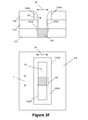
- FIG. 3F depicts the product after an etching process has been performed through the reduced-size opening 107 now defined by the internal spacer 105 A to define a trench/hole type feature 103 A in the layer of insulating material 103 .
- the etching process may be a non-negative etch bias etching process, i.e., a positive etch bias or a substantially zero etch bias etching process, that results in the trench/hole type feature 103 A having the depicted substantially vertical sidewalls (for a substantially zero etch bias process) or outwardly tapered sidewalls 103 X (shown in dashed lines) for a positive etch bias etching process.
- FIG. 1 is a non-negative etch bias etching process
- using a positive etch bias etching process to form the trench/hole type feature 103 A may actually reduce tip-to-tip, side-to-side spacing and/or tip-to-side spacing during the etching process due to the formation of the outwardly tapered sidewalls 103 X that are created when a positive etch bias etching process is used.
- the etching process performed to define the trench/hole type feature 103 A may be a negative etch bias process (as previously described) wherein the sidewalls of the trench/hole type feature 103 A would be inwardly tapered, i.e., the width of the opening at the top of the feature 103 A would be greater than the width of the opening at the bottom of the feature 103 A.
- FIG. 3H depicts the product after the patterned layer of photoresist material 104 and the internal spacer 105 A have been removed. These materials may be removed using a variety of known processes, e.g., plasma ashing, solvent rinse, etc.
- FIG. 3I depicts the product after a layer of conductive material 107 has been formed across the surface of the layer of insulating material 103 and overfills the opening 103 A. So as not to obscure the presently disclosed inventions, any associated barrier layers, seed layers and the like that may be employed as part of the process of forming the layer of conductive material 107 are not depicted in the drawings.
- the layer of conductive material 107 is intended to be representative of any type of conductive material that may be employed in forming conductive structures on an integrated circuit product.
- the layer of conductive material may be a layer of copper, aluminum, tungsten, etc.
- the layer of conductive material 107 may be formed using any of a variety of known techniques, e.g., physical vapor deposition (PVD), electroplating, electroless plating, etc.
- PVD physical vapor deposition
- FIG. 3J depicts the product after a chemical mechanical polishing (CMP) process was performed to remove excess portions of the layer of conductive material 107 positioned outside of the trench/hole type feature 103 A, which results in the conductive line-type feature 107 A.
- CMP chemical mechanical polishing
- the post-etch tip-to-tip spacing 116 PE between adjacent conductive line/hole type structures e.g., lines 107 A
- the post-etch tip-to-tip spacing 16 PE between adjacent features is less than the corresponding post-etch tip-to-tip spacing 16 PE between adjacent features when using the prior art processes described above.
- the post-etch length 112 PE of the feature 107 A is greater than the prior art post-etch length 12 PE for the corresponding feature, and the post-etch width 114 PE of the feature 107 A is less than the post-etch width 14 PE of the corresponding feature.
- the post-etch tip-to-side spacing between conductive features, e.g., conductive lines 107 A is less than the prior art post-etch tip-to-side spacing 15 PE (see FIG. 1 ), due to the reduction in the line-end-pull-back metric as a result of using the novel methods disclosed herein.
- the length or tip etch bias 118 and the width or side etch bias 120 are approximately the same due to the use of the internal spacer 105 A to uniformly reduce the size of the opening 104 A in the patterned layer of photoresist material 104 .
- the line-end-pull-back metric for the methodologies disclosed herein would be about 1.
- FIG. 3L is provided to describe another advantage the methods disclosed herein provide over the prior art methods described in the background section of this application.
- the prior art methodologies involved making the post-litho opening in the patterned layer of photoresist material as close as possible to the target dimension 14 T of the feature and thereafter performing a negative etch bias etching process to etch the opening in the underlying layer of material.
- a negative etch bias etching process to etch the opening in the underlying layer of material.
- pushing the capability limitations of the photolithography tools to form the post-litho opening as close as possible to the final target dimensions resulted in openings in the patterned layer of photoresist material that exhibit sharp tip corner rounding, as indicated by the arrow 11 in FIG. 3L .
- the size of the post-litho opening 104 A in the patterned layer of photoresist material 104 can be significantly larger than the target dimension 14 T, since the size of the opening 104 A will later be reduced by formation of the internal spacer 105 A.
- the post-litho opening 104 A in the patterned layer of photoresist material 104 will exhibit a substantially flat-shaped tip, as indicated by the arrow 111 , which leads to better tip-to-tip and tip-to-side control and better critical dimension uniformity.
- the post-litho spacing 16 PL in the prior art processes tends to be larger than the post-litho spacing 116 PL when the larger post-litho openings are employed as described herein. Accordingly, using the methods disclosed herein, the tip-to-tip and tip-to-side spacing may be reduced relative to the prior art, thereby resulting in increased packing densities.
Abstract
Description
Claims (20)
Priority Applications (1)
| Application Number | Priority Date | Filing Date | Title |
|---|---|---|---|
| US13/834,946 US8871649B2 (en) | 2013-03-15 | 2013-03-15 | Methods of forming trench/hole type features in a layer of material of an integrated circuit product |
Applications Claiming Priority (1)
| Application Number | Priority Date | Filing Date | Title |
|---|---|---|---|
| US13/834,946 US8871649B2 (en) | 2013-03-15 | 2013-03-15 | Methods of forming trench/hole type features in a layer of material of an integrated circuit product |
Publications (2)
| Publication Number | Publication Date |
|---|---|
| US20140273443A1 US20140273443A1 (en) | 2014-09-18 |
| US8871649B2 true US8871649B2 (en) | 2014-10-28 |
Family
ID=51528964
Family Applications (1)
| Application Number | Title | Priority Date | Filing Date |
|---|---|---|---|
| US13/834,946 Expired - Fee Related US8871649B2 (en) | 2013-03-15 | 2013-03-15 | Methods of forming trench/hole type features in a layer of material of an integrated circuit product |
Country Status (1)
| Country | Link |
|---|---|
| US (1) | US8871649B2 (en) |
Citations (6)
| Publication number | Priority date | Publication date | Assignee | Title |
|---|---|---|---|---|
| US5741741A (en) * | 1996-05-23 | 1998-04-21 | Vanguard International Semiconductor Corporation | Method for making planar metal interconnections and metal plugs on semiconductor substrates |
| US6127098A (en) * | 1994-02-24 | 2000-10-03 | Fujitsu Limited | Method of making resist patterns |
| US6265306B1 (en) * | 2000-01-12 | 2001-07-24 | Advanced Micro Devices, Inc. | Resist flow method for defining openings for conductive interconnections in a dielectric layer |
| US6946377B2 (en) * | 2003-10-29 | 2005-09-20 | Texas Instruments Incorporated | Multiple-gate MOSFET device with lithography independent silicon body thickness and methods for fabricating the same |
| US7711220B2 (en) * | 2008-02-13 | 2010-05-04 | Avago Technologies Fiber Ip (Singapore) Pte. Ltd. | Mode selective fiber stub, a transmitter optical subassembly that incorporates the stub and methods for making the mode selective fiber stub |
| US8083962B2 (en) * | 2006-04-06 | 2011-12-27 | Samsung Electronics Co., Ltd. | Method for forming minute pattern and method for forming semiconductor memory device using the same |
-
2013
- 2013-03-15 US US13/834,946 patent/US8871649B2/en not_active Expired - Fee Related
Patent Citations (6)
| Publication number | Priority date | Publication date | Assignee | Title |
|---|---|---|---|---|
| US6127098A (en) * | 1994-02-24 | 2000-10-03 | Fujitsu Limited | Method of making resist patterns |
| US5741741A (en) * | 1996-05-23 | 1998-04-21 | Vanguard International Semiconductor Corporation | Method for making planar metal interconnections and metal plugs on semiconductor substrates |
| US6265306B1 (en) * | 2000-01-12 | 2001-07-24 | Advanced Micro Devices, Inc. | Resist flow method for defining openings for conductive interconnections in a dielectric layer |
| US6946377B2 (en) * | 2003-10-29 | 2005-09-20 | Texas Instruments Incorporated | Multiple-gate MOSFET device with lithography independent silicon body thickness and methods for fabricating the same |
| US8083962B2 (en) * | 2006-04-06 | 2011-12-27 | Samsung Electronics Co., Ltd. | Method for forming minute pattern and method for forming semiconductor memory device using the same |
| US7711220B2 (en) * | 2008-02-13 | 2010-05-04 | Avago Technologies Fiber Ip (Singapore) Pte. Ltd. | Mode selective fiber stub, a transmitter optical subassembly that incorporates the stub and methods for making the mode selective fiber stub |
Also Published As
| Publication number | Publication date |
|---|---|
| US20140273443A1 (en) | 2014-09-18 |
Similar Documents
| Publication | Publication Date | Title |
|---|---|---|
| US10242952B2 (en) | Registration mark formation during sidewall image transfer process | |
| US8753940B1 (en) | Methods of forming isolation structures and fins on a FinFET semiconductor device | |
| US9123656B1 (en) | Organosilicate polymer mandrel for self-aligned double patterning process | |
| US20170025519A1 (en) | Method of fabricating semiconductor device | |
| US7977237B2 (en) | Fabricating vias of different size of a semiconductor device by splitting the via patterning process | |
| US10930505B2 (en) | Methods for integrated circuit design and fabrication | |
| US10026647B2 (en) | Multi-metal fill with self-align patterning | |
| US8932961B2 (en) | Critical dimension and pattern recognition structures for devices manufactured using double patterning techniques | |
| KR20110081833A (en) | Contacts and vias of a semiconductor device formed by a hardmask and double exposure | |
| US11769691B2 (en) | Semiconductor device and formation method thereof | |
| US9564371B2 (en) | Method for forming semiconductor device | |
| TWI726370B (en) | Semiconductor device with reduced critical dimensions and method of manufacturing the same | |
| US9324577B2 (en) | Modified self-aligned contact process and semiconductor device | |
| US9287109B2 (en) | Methods of forming a protection layer to protect a metal hard mask layer during lithography reworking processes | |
| CN110931354B (en) | Semiconductor structure and method for manufacturing semiconductor structure | |
| US20220277984A1 (en) | Contact Resistance Between Via and Conductive Line | |
| US9748139B1 (en) | Method of fabricating dual damascene structure | |
| US8871649B2 (en) | Methods of forming trench/hole type features in a layer of material of an integrated circuit product | |
| US9711369B2 (en) | Method for forming patterns with sharp jogs | |
| US10685871B2 (en) | Method for forming semiconductor structure | |
| US10103019B1 (en) | Manufacturing method for forming a semiconductor structure |
Legal Events
| Date | Code | Title | Description |
|---|---|---|---|
| AS | Assignment |
Owner name: RENESAS ELECTRONICS CORPORATION, JAPAN Free format text: ASSIGNMENT OF ASSIGNORS INTEREST;ASSIGNOR:MATSUI, YOSHINORI;REEL/FRAME:032744/0854 Effective date: 20130311 Owner name: GLOBALFOUNDRIES INC., CAYMAN ISLANDS Free format text: ASSIGNMENT OF ASSIGNORS INTEREST;ASSIGNOR:JANG, LINUS;REEL/FRAME:032747/0041 Effective date: 20130303 |
|
| AS | Assignment |
Owner name: INTERNATIONAL BUSINESS MACHINES CORPORATION, NEW Y Free format text: ASSIGNMENT OF ASSIGNORS INTEREST;ASSIGNOR:TSENG, CHIAHSUN;REEL/FRAME:033837/0211 Effective date: 20140926 |
|
| STCF | Information on status: patent grant |
Free format text: PATENTED CASE |
|
| MAFP | Maintenance fee payment |
Free format text: PAYMENT OF MAINTENANCE FEE, 4TH YEAR, LARGE ENTITY (ORIGINAL EVENT CODE: M1551) Year of fee payment: 4 |
|
| AS | Assignment |
Owner name: WILMINGTON TRUST, NATIONAL ASSOCIATION, DELAWARE Free format text: SECURITY AGREEMENT;ASSIGNOR:GLOBALFOUNDRIES INC.;REEL/FRAME:049490/0001 Effective date: 20181127 |
|
| AS | Assignment |
Owner name: GLOBALFOUNDRIES U.S. INC., CALIFORNIA Free format text: ASSIGNMENT OF ASSIGNORS INTEREST;ASSIGNOR:GLOBALFOUNDRIES INC.;REEL/FRAME:054633/0001 Effective date: 20201022 |
|
| AS | Assignment |
Owner name: GLOBALFOUNDRIES INC., CAYMAN ISLANDS Free format text: RELEASE BY SECURED PARTY;ASSIGNOR:WILMINGTON TRUST, NATIONAL ASSOCIATION;REEL/FRAME:054636/0001 Effective date: 20201117 |
|
| AS | Assignment |
Owner name: GLOBALFOUNDRIES U.S. INC., NEW YORK Free format text: RELEASE BY SECURED PARTY;ASSIGNOR:WILMINGTON TRUST, NATIONAL ASSOCIATION;REEL/FRAME:056987/0001 Effective date: 20201117 |
|
| FEPP | Fee payment procedure |
Free format text: MAINTENANCE FEE REMINDER MAILED (ORIGINAL EVENT CODE: REM.); ENTITY STATUS OF PATENT OWNER: LARGE ENTITY |
|
| LAPS | Lapse for failure to pay maintenance fees |
Free format text: PATENT EXPIRED FOR FAILURE TO PAY MAINTENANCE FEES (ORIGINAL EVENT CODE: EXP.); ENTITY STATUS OF PATENT OWNER: LARGE ENTITY |
|
| STCH | Information on status: patent discontinuation |
Free format text: PATENT EXPIRED DUE TO NONPAYMENT OF MAINTENANCE FEES UNDER 37 CFR 1.362 |
|
| FP | Lapsed due to failure to pay maintenance fee |
Effective date: 20221028 |