US8860174B2 - Recessed antifuse structures and methods of making the same - Google Patents
Recessed antifuse structures and methods of making the same Download PDFInfo
- Publication number
- US8860174B2 US8860174B2 US11/495,805 US49580506A US8860174B2 US 8860174 B2 US8860174 B2 US 8860174B2 US 49580506 A US49580506 A US 49580506A US 8860174 B2 US8860174 B2 US 8860174B2
- Authority
- US
- United States
- Prior art keywords
- antifuse
- trench
- access device
- work function
- recessed access
- Prior art date
- Legal status (The legal status is an assumption and is not a legal conclusion. Google has not performed a legal analysis and makes no representation as to the accuracy of the status listed.)
- Active, expires
Links
Images


Classifications
-
- H01L21/823425—
-
- H—ELECTRICITY
- H10—SEMICONDUCTOR DEVICES; ELECTRIC SOLID-STATE DEVICES NOT OTHERWISE PROVIDED FOR
- H10W—GENERIC PACKAGES, INTERCONNECTIONS, CONNECTORS OR OTHER CONSTRUCTIONAL DETAILS OF DEVICES COVERED BY CLASS H10
- H10W20/00—Interconnections in chips, wafers or substrates
- H10W20/40—Interconnections external to wafers or substrates, e.g. back-end-of-line [BEOL] metallisations or vias connecting to gate electrodes
- H10W20/49—Adaptable interconnections, e.g. fuses or antifuses
- H10W20/491—Antifuses, i.e. interconnections changeable from non-conductive to conductive
-
- H01L21/82345—
-
- H01L29/66621—
-
- H—ELECTRICITY
- H10—SEMICONDUCTOR DEVICES; ELECTRIC SOLID-STATE DEVICES NOT OTHERWISE PROVIDED FOR
- H10D—INORGANIC ELECTRIC SEMICONDUCTOR DEVICES
- H10D64/00—Electrodes of devices having potential barriers
- H10D64/01—Manufacture or treatment
- H10D64/025—Manufacture or treatment forming recessed gates, e.g. by using local oxidation
- H10D64/027—Manufacture or treatment forming recessed gates, e.g. by using local oxidation by etching at gate locations
-
- H—ELECTRICITY
- H10—SEMICONDUCTOR DEVICES; ELECTRIC SOLID-STATE DEVICES NOT OTHERWISE PROVIDED FOR
- H10D—INORGANIC ELECTRIC SEMICONDUCTOR DEVICES
- H10D84/00—Integrated devices formed in or on semiconductor substrates that comprise only semiconducting layers, e.g. on Si wafers or on GaAs-on-Si wafers
- H10D84/01—Manufacture or treatment
- H10D84/0123—Integrating together multiple components covered by H10D12/00 or H10D30/00, e.g. integrating multiple IGBTs
- H10D84/0126—Integrating together multiple components covered by H10D12/00 or H10D30/00, e.g. integrating multiple IGBTs the components including insulated gates, e.g. IGFETs
- H10D84/013—Manufacturing their source or drain regions, e.g. silicided source or drain regions
- H10D84/0133—Manufacturing common source or drain regions between multiple IGFETs
-
- H—ELECTRICITY
- H10—SEMICONDUCTOR DEVICES; ELECTRIC SOLID-STATE DEVICES NOT OTHERWISE PROVIDED FOR
- H10D—INORGANIC ELECTRIC SEMICONDUCTOR DEVICES
- H10D84/00—Integrated devices formed in or on semiconductor substrates that comprise only semiconducting layers, e.g. on Si wafers or on GaAs-on-Si wafers
- H10D84/01—Manufacture or treatment
- H10D84/0123—Integrating together multiple components covered by H10D12/00 or H10D30/00, e.g. integrating multiple IGBTs
- H10D84/0126—Integrating together multiple components covered by H10D12/00 or H10D30/00, e.g. integrating multiple IGBTs the components including insulated gates, e.g. IGFETs
- H10D84/0135—Manufacturing their gate conductors
- H10D84/014—Manufacturing their gate conductors the gate conductors having different materials or different implants
-
- H—ELECTRICITY
- H10—SEMICONDUCTOR DEVICES; ELECTRIC SOLID-STATE DEVICES NOT OTHERWISE PROVIDED FOR
- H10D—INORGANIC ELECTRIC SEMICONDUCTOR DEVICES
- H10D84/00—Integrated devices formed in or on semiconductor substrates that comprise only semiconducting layers, e.g. on Si wafers or on GaAs-on-Si wafers
- H10D84/01—Manufacture or treatment
- H10D84/02—Manufacture or treatment characterised by using material-based technologies
- H10D84/03—Manufacture or treatment characterised by using material-based technologies using Group IV technology, e.g. silicon technology or silicon-carbide [SiC] technology
- H10D84/038—Manufacture or treatment characterised by using material-based technologies using Group IV technology, e.g. silicon technology or silicon-carbide [SiC] technology using silicon technology, e.g. SiGe
-
- H—ELECTRICITY
- H10—SEMICONDUCTOR DEVICES; ELECTRIC SOLID-STATE DEVICES NOT OTHERWISE PROVIDED FOR
- H10W—GENERIC PACKAGES, INTERCONNECTIONS, CONNECTORS OR OTHER CONSTRUCTIONAL DETAILS OF DEVICES COVERED BY CLASS H10
- H10W20/00—Interconnections in chips, wafers or substrates
- H10W20/01—Manufacture or treatment
- H10W20/031—Manufacture or treatment of conductive parts of the interconnections
- H10W20/056—Manufacture or treatment of conductive parts of the interconnections by filling conductive material into holes, grooves or trenches
- H10W20/057—Manufacture or treatment of conductive parts of the interconnections by filling conductive material into holes, grooves or trenches by selectively depositing, e.g. by using selective CVD or plating
Definitions
- the invention relates to antifuse devices and, more particularly, to recessed gate dielectric antifuse devices and methods of making the same.
- Antifuse devices are commonly used to permanently program integrated circuit (IC) devices and other electrical components.
- Semiconductor integrated circuit devices such as flash memory, erasable programmable read-only memory (EPROM), electrically erasable programmable read-only memory (EEPROM), dynamic random access memory (DRAM), static random access memory (SRAM), and other random access memory devices typically employ the use of antifuses to program the memory or to provide access to redundant circuitry in the memory devices.
- memory devices and other integrated circuit devices frequently include redundant circuitry linked to operational circuitry by one or more antifuse devices. In those instances where the operational circuitry fails or is defective, one or more antifuses may be programmed to bypass the defective circuitry or to utilize available redundant circuitry in place of the defective circuitry.
- the use of antifuses to program conventional integrated circuit devices and to select circuitry to be used on an integrated circuit device is well known.
- Gate-oxide antifuses are typically formed from conventional planar access devices (PAD) such as Metal Oxide Semiconductor Field Effect Transistors (MOSFET).
- MOSFETs generally include a doped polysilicon gate, a channel conduction region, and source/drain regions formed by diffusion of dopants in silicon substrates.
- a voltage difference may be generated between the doped polysilicon gate and the channel conduction region or the source/drain regions of the MOSFET.
- the voltage difference may be used to program the antifuse device.
- antifuses have a high resistance; when a high voltage exceeding the capacity of the antifuse is applied across the antifuse, the gate-oxide of the antifuse breaks down, creating an electrically conductive path through the antifuse.
- the breakdown of an antifuse may include a soft breakdown, where the antifuse has a high fuse resistance, or a hard breakdown, where the antifuse has a low fuse resistance.
- antifuses formed from recessed access devices as opposed to the traditional planar access devices (PAD) are being used with high-density memory cells.
- Recessed access device antifuses are described in U.S. patent application Ser. No. 10/933,161, now U.S. Pat. No. 7,795,094, issued Sep. 14, 2010, entitled “RECESSED GATE DIELECTRIC ANTIFUSE,” and published as US 2006/0046354, the disclosure of which is incorporated herein by reference in its entirety.
- the use of recessed access devices as antifuses allows the formation of smaller antifuses with integrated circuits and semiconductor devices. This is especially desirable, as the design of integrated circuit devices require smaller feature sizes and increased circuit densities.
- FIG. 1 illustrates a cross-sectional view of a recessed access device structure that may be used as an antifuse according to embodiments of the invention
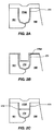
- FIGS. 2A-2E illustrate cross-sectional views of various process steps in the fabrication the recessed access device antifuse illustrated in FIG. 1 according to embodiments of the invention
- FIG. 3 illustrates a cross-sectional view of the recessed access device antifuse illustrated in FIG. 1 showing breakdown areas according to embodiments of the invention
- FIG. 4 illustrates a cross-sectional view of a recessed access device antifuse that may be used as an antifuse according to embodiments of the invention
- FIGS. 5A-5C illustrate cross-sectional views of various process steps in the fabrication of the recessed access device antifuse illustrated in FIG. 4 according to embodiments of the invention
- FIG. 6 illustrates a cross-sectional view of a spherical recessed access device antifuse according to embodiments of the invention
- FIGS. 7A-7D illustrate cross-sectional views of various process steps in the fabrication of the spherical recessed access device antifuse illustrated in FIG. 6 according to embodiments of the invention
- FIG. 8 illustrates a cross-sectional view of a spherical recessed access device antifuse according to embodiments of the invention
- FIGS. 9A-9C illustrate cross-sectional views of various process steps in the fabrication of the spherical recessed access device antifuse illustrated in FIG. 8 according to embodiments of the invention.
- FIG. 10 illustrates a cross-sectional view of a spherical recessed access device antifuse according to embodiments of the invention.
- FIG. 11 illustrates a top-down view of an integrated circuit device employing a recessed access device antifuse according to embodiments of the invention.
- antifuses for use with integrated circuits and semiconductor devices may be formed utilizing recessed access devices and spherical recessed access devices.
- the antifuses may include two or more materials having different work function values.
- the work function values of the two or more materials used with the antifuses may differ by about 0.2 eV or more.
- the difference in work function values of the materials used to form the antifuses of embodiments of the invention allows the antifuses to be customized such that the breakdown areas of the antifuses may be controlled.
- a recessed access device having two or more materials with different work function values layered on top of each other may be used as an antifuse device with integrated circuitry and semiconductor devices.
- the layered materials may be separated by one or more barrier layers for preventing migration of dopants from one material to another during integrated circuit and semiconductor fabrication processes.
- the recessed access device having two or more material layers may be a spherical recessed access device. The intersection of each of the two or more layers of materials in the recessed access device provides a likely area for antifuse breakdown. Utilizing the likely breakdown area, the breakdown of the antifuse may be controlled or tailored for a desired function or for use with a desired integrated circuit or semiconductor device.
- a recessed access device having two or more materials aligned vertically in a trench defining the recessed access device may have different work function values.
- a first material may be positioned on the sidewalls of the recessed access device with one or more additional materials filling the remainder of the recessed access device and at least partially surrounded by the first material.
- the difference in the work function values of the first material and the one or more additional materials may be about 0.2 eV or more.
- the recessed access device may be a spherical recessed access device. The intersection of each of the two or more layers of materials in the recessed access device provides a likely area for antifuse breakdown. Utilizing the likely breakdown area, the breakdown of the antifuse may be controlled or tailored for a desired function or for use with a desired integrated circuit or semiconductor device.
- an antifuse may be formed from a recessed access device (RAD) structure or a spherical recessed access device (SRAD) structure.
- the RAD structure or the SRAD structure may be formed, in part, from two or more materials having different work functions. The intersections of the different work function materials in the RAD structures or the SRAD structures provide a convenient location for antifuse breakdown.
- the partial spherical shape of SRAD structures provides additional breakdown locations for antifuses formed from such structures.
- the antifuse device 150 may include one or more recessed access device (RAD) antifuses 170 .
- a RAD antifuse 170 may be formed in a trench of a semiconductor substrate 160 and may be positioned between active areas 162 , such as between laterally spaced source and drain regions of memory devices, or between source and drain regions and shallow trench isolation (STI) regions 161 as illustrated in FIG. 1 .
- the trench in the semiconductor substrate 160 may be lined with an oxide 171 similar to the gate-oxide linings used with conventional RAD structures.
- the RAD antifuse 170 may include a first material 172 overlying a second material 174 in the trench of the semiconductor substrate 160 .
- the first material 172 and the second material 174 may be separated by a barrier 173 as illustrated in FIG. 1 .
- the RAD antifuse 170 may also include a gate overlying the first material 172 .
- the gate may include a strap 176 overlying the first material 172 and an insulator cap 180 overlying the strap 176 .
- the RAD antifuse 170 may include an insulator cap 180 without a strap 176 .
- Sidewall spacers 178 may also be formed with the RAD antifuse 170 .
- the second material 174 of the RAD antifuse 170 may be formed of a material having a higher work function than the first material 172 .
- the second material 174 may include a p-type doped polysilicon material and the first material 172 may include an n-type doped polysilicon material.
- the second material 174 would exhibit a higher work function than that of the first material 172 in the n-channel device.
- the second material 174 may include an n-type doped polysilicon material and the first material 172 may include a p-type doped polysilicon material.
- Other materials having differing work functions may also be used to form a RAD antifuse 170 according to embodiments of the invention.
- Materials used to form the first material 172 and second material 174 may include materials such as polysilicon, doped polysilicon, metals, and metal alloys.
- a barrier 173 may be positioned between the first material 172 and the second material 174 in the RAD antifuse 170 to prevent cross-diffusion of dopants in the first material 172 and second material 174 .
- the barrier 173 may also provide an ohmic contact between the two materials if desired.
- the barrier 173 may include metals such as tungsten, aluminum, copper, or titanium.
- the barrier 173 may be formed from one or more metal layers, including similar or dissimilar metals.
- the barrier 173 may provide an electrical connection or conduction between the first material 172 and the second material 174 .
- the barrier 173 may also act as an insulator or may be formed from conductive material, insulative material, or conductive and insulative material.
- the strap 176 may be formed of a conductive material, such as a metal, a conductive silicon material, a doped silicon material, or another conductor. In other embodiments, the strap 176 need not be conductive.
- An insulator cap 180 incorporated with a RAD antifuse 170 may include any insulating material that may be used as an insulating layer for conventional planar or recessed access devices.
- the insulator cap 180 may be formed of a nitride or an oxide such as silicon nitride or silicon dioxide.
- sidewall spacers 178 may be formed from materials used to form spacers 178 with conventional planar or recessed access devices.
- the sidewall spacers 178 may include materials such as silicon dioxide or other oxides, silicon nitride, or other nitrides, or silicon oxynitride.
- the sidewall spacers 178 and the insulator cap 180 may be formed of the same material.
- the RAD antifuse 170 of embodiments of the invention may be produced using fabrication processes used to form conventional RAD structures in semiconductor devices and particularly memory devices.
- the RAD antifuse 170 illustrated in FIG. 1 may be formed using conventional CMOS or memory device fabrication processes similar to the processes illustrated in FIGS. 2A-2E .
- a semiconductor substrate 160 having one or more trenches formed therein may be provided.
- the one or more trenches may be formed next to or in part of a shallow trench isolation region 161 or between active areas 162 in the semiconductor substrate 160 , or regions where active areas 162 are to be formed.
- Oxide 171 may be grown or deposited in a trench using conventional oxide formation processes.
- a second material layer 174 A may be deposited over the semiconductor substrate 160 and in the trenches and may be doped using conventional processes. Masking and/or etching of the second material layer 174 A may be performed to form the second material 174 in the bottoms of the trenches of the semiconductor substrate 160 as illustrated in FIG. 2B .
- a barrier layer 173 A may be deposited over the second material 174 and the semiconductor substrate 160 . Masking and/or etching of the barrier layer 173 A may form a barrier 173 over the second material 174 in the bottom of the trenches as illustrated in FIG. 2C .
- a first material layer 172 A may be deposited over the semiconductor substrate 160 and in the trenches over the barrier 173 as illustrated in FIG. 2C .
- Masking and/or etching of the first material layer 172 A may form the first material 172 as illustrated in FIG. 2D .
- the masking and/or etching of the first material layer 172 A may be performed such that a portion of the first material 172 extends above a surface of the semiconductor substrate 160 .
- An optional strap material 176 A deposited over the first material 172 may be masked and/or etched to form a strap 176 over the first material 172 as illustrated in FIG. 2E .
- Conventional masking, etching, doping, and deposition processes may be used to complete the formation of the RAD antifuse 170 illustrated in FIG. 1 , including the formation of insulator caps 180 and sidewall spacers 178 if desired, and the doping of the active areas 162 where required.
- FIGS. 2A-2E Although particular methods for forming the RAD antifuse 170 of certain embodiments of the invention are illustrated in FIGS. 2A-2E , it is understood that other methods and processes may also be used to fabricate RAD antifuses 170 according to embodiments of the invention.
- the utilization of multi-work function materials to fabricate the RAD antifuses 170 may provide improved breakdown areas 190 A, 190 B in the RAD antifuse 170 as compared to traditional recessed access device antifuse structures, such as those described in the afore-mentioned U.S. patent application Ser. No. 10/933,161, entitled “RECESSED GATE DIELECTRIC ANTIFUSE,” and published as US 2006/0046354, now U.S. Pat. No. 7,795,095, issued Sep. 14, 2010.
- the RAD antifuse 170 of FIG. 1 may include one or more likely breakdown areas 190 A, 190 B represented by the circled areas in FIG. 3 .
- Breakdown area 190 A is a likely breakdown area for the RAD antifuse 170 because of the disruption in the oxide 171 that occurs at the intersection of the first material 172 and the second material 174 with or without a barrier 173 .
- a second likely breakdown area 190 B occurs at the intersection between the semiconductor substrate 160 , the active area 162 , and the oxide 171 .
- the curvature of the bottom of RAD antifuse 170 in the trench of the semiconductor substrate 160 may also enhance a generated electric field in the RAD antifuse 170 , contributing to improved breakdown of the RAD antifuse 170 .
- RAD antifuse 170 in an integrated circuit device or semiconductor device may allow the customization of the antifuse positioning to produce a breakdown of the antifuse in a desired region of the integrated circuit device or semiconductor device.
- an antifuse device 150 ′ having one or more RAD antifuses 170 ′ with two or more materials having different work functions may include a RAD antifuse 170 ′ having a first material 172 ′ positioned along at least a portion of the sidewalls of the RAD antifuse 170 ′ and a second material 174 ′ at least partially surrounded by the first material 172 ′ as illustrated in FIG. 4 .
- trenches in the semiconductor substrate 160 ′ may include an oxide 171 ′ on the sidewalls and in the bottom of the trenches.
- the first material 172 ′ may be positioned along at least a portion of the oxide 171 ′ layer and the second material 174 ′ may be positioned in an interior portion of the trench with respect to the first material 172 ′, or within an opening in the first material 172 ′, as illustrated.
- a barrier layer (not shown) may be formed between the first material 172 ′ and the second material 174 ′.
- the RAD antifuse 170 ′ may also include a gate overlying the first material 172 ′ and second material 174 ′.
- the gate may include a strap 176 ′ overlying the first material 172 ′ and second material 174 ′ and an insulator cap 180 ′ overlying the strap 176 ′.
- Sidewall spacers 178 ′ may also be formed with the RAD antifuse 170 ′.
- the RAD antifuse 170 ′ may be positioned between active areas 162 ′, such as source and drain regions of memory devices, or between a source or drain region active area 162 ′ and a shallow trench isolation (STI) region 161 ′ as illustrated in FIG. 4 .
- active areas 162 ′ such as source and drain regions of memory devices, or between a source or drain region active area 162 ′ and a shallow trench isolation (STI) region 161 ′ as illustrated in FIG. 4 .
- STI shallow trench isolation
- the most likely point of breakdown in the RAD antifuse 170 ′ is located at the intersection of the first material 172 ′ and the second material 174 ′ with the oxide 171 ′, as illustrated by a circled breakdown area 190 ′.
- a voltage sufficient to break the RAD antifuse 170 ′ is applied to the RAD antifuse 170 ′, the breakdown of the RAD antifuse 170 ′ will most likely occur within or near the breakdown area 190 ′.
- the breakdown area 190 ′ is a likely breakdown point for the RAD antifuse 170 ′ because of the disruption of the oxide 171 ′ due to the convergence of the first material 172 ′ and the second material 174 ′ within the breakdown area 190 ′.
- the second material 174 ′ of the RAD antifuse 170 ′ may be formed of a material having a higher work function than the first material 172 ′.
- the second material 174 ′ illustrated in FIG. 4 is used with an n-doped channel device, the second material 174 ′ may include a p-doped polysilicon material and the first material 172 ′ may include an n-doped polysilicon material.
- Other materials having differing work functions may also be used to form RAD antifuse 170 ′ according to embodiments of the invention.
- materials used to form the first material 172 ′ and second material 174 ′ may include materials such as polysilicon, doped polysilicon, metals, and metal alloys.
- the RAD antifuse 170 ′ of embodiments of the invention may be produced using fabrication processes used to form conventional semiconductor devices and particularly memory devices.
- the RAD antifuse 170 ′ illustrated in FIG. 4 may be formed using conventional CMOS or memory device fabrication processes similar to the steps illustrated in FIGS. 5A-5C .
- a semiconductor substrate 160 ′ having trenches formed therein may be provided.
- Oxide 171 ′ may be grown or deposited in the trenches in a manner similar to conventional RAD structures.
- a first material layer 172 A′, such as polysilicon, may be deposited over the semiconductor substrate 160 ′ and in the trenches.
- the first material layer 172 A′ may be doped according to conventional doping techniques if desired.
- An anisotropic spacer etch selective to the oxide 171 ′ may be performed to remove the first material layer 172 A′ in the bottom of a trench, leaving the first material 172 ′ on the sidewalls of the trench as illustrated in FIG. 5B .
- a second material layer 174 A′ formed of a material having a higher work function than the first material 172 ′ may be deposited over the substrate 160 ′ and in the trenches as illustrated in FIG. 5B .
- Masking and/or etching of the second material layer 174 A′ may be used to form the second material 174 ′ as illustrated in FIG. 5C .
- the second material 174 ′ may also be doped using conventional processes as desired.
- RAD antifuse 170 ′ Conventional masking, etching, doping, and deposition processes may be used to complete the formation of a RAD antifuse 170 ′, including the formation of a strap 176 ′, formation of insulator caps 180 ′, and formation of sidewall spacers 178 ′ as illustrated in FIG. 4 .
- Active areas 162 ′ may also be formed in the semiconductor substrate 160 ′ according to conventional methods.
- FIGS. 5A-5C Although particular methods for forming the RAD antifuse 170 ′ of certain embodiments of the invention are illustrated in FIGS. 5A-5C , it is understood that other methods and processes may also be used to fabricate RAD antifuse 170 ′ according to embodiments of the invention.
- Spherical recessed access devices may also be used as antifuses according to other embodiments of the invention.
- SRAD antifuse 270 according to particular embodiments of the invention is illustrated in FIG. 6 .
- the SRAD antifuse 270 may include the same characteristics as RAD antifuses 170 of embodiments of the invention and may be formed using similar processes. However, as illustrated in FIG. 6 , the difference between the SRAD antifuse 270 and the RAD antifuse 170 is the partially or substantially spherically shaped bottom portion of the SRAD antifuse 270 .
- the SRAD antifuse 270 illustrated in FIG. 6 is formed in a trench of a semiconductor substrate 260 and may be positioned between active areas 262 , such as between source and drain regions of semiconductor devices, or between source and drain regions and shallow trench isolation (STI) regions 262 as illustrated in FIG. 6 .
- the trench in an SRAD antifuse 270 configuration includes a partially spherical or substantially spherical opening in the bottom of the trench as known with conventional spherical recessed access devices.
- the trench of an SRAD antifuse 270 may be lined with an oxide 271 material.
- a first material 272 may overlie a second material 274 in the trench of the semiconductor substrate 260 .
- the first material 272 and the second material 274 may be separated by a barrier 273 as illustrated in FIG. 6 .
- the SRAD antifuses 270 may also include a gate over the first material 272 .
- the gate may include strap layers 276 , insulator caps 280 , and sidewall spacers 278 as desired.
- the SRAD antifuse 270 illustrated in FIG. 6 includes a strap layer 276 overlying the first material 272 .
- An insulator cap 280 overlies the strap layer 276 and is in contact with sidewall spacers 278 .
- Strap layers 276 , insulator caps 280 , and sidewall spacers 278 utilized with SRAD antifuses 270 according to embodiments of the invention may be formed using the same materials and procedures that are used to form similar structures for the RAD antifuses 170 according to embodiments of the invention.
- the first material 272 and second material 274 used to form SRAD antifuses 270 may be formed of materials having different work functions.
- the first material 272 may have a lower work function than the second material 274 ; in an n-channel device, the second material 274 may include a p-type doped polysilicon material while the first material 272 may include an n-type doped polysilicon material, providing a first material 272 with a lower work function than the second material 274 .
- Other materials may also be used to form the materials of the SRAD antifuse 270 according to various embodiments of the invention.
- the SRAD antifuse 270 illustrated in FIG. 6 may be produced using fabrication processes used to form conventional SRAD structures in semiconductor devices, and particularly in memory devices.
- One process that may be used to fabricate the SRAD antifuse 270 illustrated in FIG. 6 is similar to conventional CMOS or memory device fabrication processes and is illustrated in FIGS. 7A-7D .
- a semiconductor substrate 260 having one or more trenches with partially spherical or substantially spherical bottom trench portions may be provided.
- the trenches may be formed next to or in part of a shallow trench isolation region 261 or in proximity to regions in the semiconductor substrate 260 which may be formed into active areas (not shown).
- An oxide 271 layer may be grown or deposited in a trench using conventional oxide formation processes.
- a second material layer 274 A such as a polysilicon layer, may be deposited over the semiconductor substrate 260 and in the trench. Masking and/or etching of the second material layer 274 A may be performed to form a second material 274 within the trench as illustrated in FIG. 7B . The masking and/or etching may be controlled such that a desired amount of second material 274 remains in the trench.
- a barrier layer 273 A may be deposited over the second material 274 and the semiconductor substrate 260 . Masking and/or etching of the barrier layer 273 A may form barrier 273 over the second material 274 in a spherical trench as illustrated in FIG. 7C .
- a first material layer 272 A such as polysilicon, may be deposited over the semiconductor substrate 260 and in the trench over the barrier 273 as illustrated in FIG. 7C .
- Masking and/or etching of the first material layer 272 A may form the first material 272 as illustrated in FIG. 7D .
- the masking and/or etching of the first material layer 272 A may be performed such that a portion of the first material 272 extends above a surface of the semiconductor substrate 260 .
- Conventional masking, etching, doping, and deposition processes may be used to complete the formation of the SRAD antifuse 270 , including the formation of strap layers 276 , insulator caps 280 and sidewall spacers 278 if desired.
- Doping of the semiconductor substrate 260 to form one or more active areas 262 may also be performed as desired.
- FIGS. 7A-7D Although a fabrication method for SRAD antifuse 270 devices is illustrated in FIGS. 7A-7D , it is understood that other methods and processes may also be used to fabricate SRAD antifuses 270 according to embodiments of the invention.
- an SRAD antifuse 270 may include one or more likely breakdown areas 290 represented by the circled areas in FIG. 6 .
- One likely breakdown area 290 occurs at the intersection between the first material 272 and the second material 274 with the oxide 271 or at the intersection of the two materials with the barrier 273 and the oxide 271 , next to the active area 262 .
- the likely breakdown area 290 for the SRAD antifuse 270 occurs because of the disruption in the oxide 271 that occurs at the intersection of the first material 272 and the second material 274 with or without a barrier 273 .
- the intersection between the first material 272 and the second material 274 with the oxide 271 occurs at the pinched region of the SRAD antifuse 270 trench where the partially spherical bottom portion of the trench meets with the upper portion of the trench. Even if the first material 272 and second material 274 of an SRAD antifuse 270 do not meet at the pinched region of the SRAD antifuse 270 , the pinched region itself may create a likely breakdown area 290 for the SRAD antifuse 270 .
- an antifuse device 250 ′ having one or more SRAD antifuses 270 ′ with two or more materials having different work functions may include an SRAD antifuse 270 ′ having a first material 272 ′ positioned along at least a portion of the sidewalls of a partially spherically shaped trench in a semiconductor substrate 260 ′ and a second material 274 ′ at least partially surrounded by the first material 272 ′ as illustrated in FIG. 8 .
- trenches in a semiconductor substrate 260 ′ may include an oxide 271 ′ layer on the sidewalls and in the bottom of the trenches.
- the first material 272 ′ may be positioned along at least a portion of the oxide 271 ′ layer and the second material 274 ′ may be positioned in an interior portion of the trenches with respect to the first material 272 ′, or in an opening in the first material 272 ′, as illustrated.
- a barrier layer (not shown) may be formed between the first material 272 ′ and the second material 274 ′.
- the SRAD antifuse 270 ′ may also include a gate overlying the first material 272 ′ and the second material 274 ′.
- the gate may include a strap 276 ′ overlying the first material 272 ′ and second material 274 ′ and an insulator cap 280 ′ overlying the strap 276 ′.
- SRAD antifuse 270 ′ may also be formed with the SRAD antifuse 270 ′ as desired.
- the SRAD antifuse 270 ′ may be positioned between active areas 262 ′, such as between source and drain regions of memory devices, or between a source or drain region active area 262 ′ and a shallow trench isolation region 261 ′ as illustrated in FIG. 8 .
- the SRAD antifuse 270 ′ illustrated in FIG. 8 includes at least two likely breakdown areas 290 A′, 290 B′.
- a first likely breakdown area 290 A′ occurs at the intersection of the first material 272 ′ and the second material 274 ′ with the oxide 271 ′ in proximity to the active area 262 ′.
- a second likely breakdown area 290 B′ occurs at the pinched section of the SRAD antifuse 270 ′ trench where the partially spherical bottom portion of the trench meets with the upper portion of the trench as illustrated in FIG. 8 .
- the first likely breakdown area 290 A′ is a likely point for SRAD antifuse 270 ′ breakdown because of the disruption of the oxide 271 ′ caused by the intersection of the first material 272 ′ and the second material 274 ′ within the first likely breakdown area 290 A′.
- the second likely breakdown area 290 B′ may be more likely to breakdown under high voltage due to the different thicknesses of the first material 272 ′ converging within the second likely breakdown area 290 B′ in the SRAD antifuse 270 ′.
- the second material 274 ′ of the SRAD antifuse 270 ′ may be formed of a material having a higher work function than the first material 272 ′.
- the second material 274 ′ used to form the SRAD antifuse 270 ′ illustrated in FIG. 8 may include a p-doped polysilicon material and the first material 272 ′ may include an n-doped polysilicon material.
- Other materials having differing work functions may also be used to form SRAD antifuse 270 ′ according to embodiments of the invention.
- the SRAD antifuse 270 ′ of embodiments of the invention may be produced using fabrication processes used to form conventional semiconductor devices and particularly memory devices.
- the SRAD antifuse 270 ′ illustrated in FIG. 8 may be formed using conventional CMOS or memory device fabrication processes similar to the steps illustrated in FIGS. 9A-9C .
- a semiconductor substrate 260 ′ having partially spherically shaped trenches formed therein may be provided.
- Oxide 271 ′ may be grown or deposited in the trenches as with conventional SRAD structures.
- a first material layer 272 A′ may be deposited over the semiconductor substrate 260 ′ and in the trenches.
- the first material layer 272 A′ may be doped according to conventional doping techniques.
- An anisotropic spacer etch selective to the oxide 271 ′ may be performed to remove the first material layer 272 A′ in the bottom of a trench, leaving the first material 272 ′ on the sidewalls of the trench as illustrated in FIG. 9B .
- a second material layer 274 A′ may be deposited over the substrate 260 ′ and in the trenches as illustrated in FIG. 9B .
- the second material layer 274 A′ may be doped according to conventional methods as desired. Masking and/or etching of the second material layer 274 A′ may be used to form the second material 274 ′ as illustrated in FIG. 9C ; the second material 274 ′ having a higher work function than the first material 272 ′.
- SRAD antifuse 270 ′ Conventional masking, etching, doping, and deposition processes may be used to complete the formation of an SRAD antifuse 270 ′, including the formation of a strap 276 ′, formation of insulator caps 280 ′, and formation of sidewall spacers 278 ′ as illustrated in FIG. 8 .
- Active areas 262 ′ may also be formed in the semiconductor substrate 260 ′ according to conventional methods.
- FIGS. 9A-9C Although methods for forming an SRAD antifuse 270 ′ according to particular embodiments of the invention are illustrated in FIGS. 9A-9C , it is understood that other methods and processes may also be used to fabricate SRAD antifuses 270 ′ according to embodiments of the invention.
- the RAD antifuses and SRAD antifuses illustrated in FIGS. 1 , 4 , 6 , and 8 each include two material layers, it is understood that in other particular embodiments of the invention, the RAD antifuses and SRAD antifuses may include two or more layers of different materials.
- an SRAD antifuse 370 similar to that illustrated in FIG. 6 is illustrated in FIG. 10 .
- the SRAD antifuse 370 may include an oxide 371 in a spherically shaped trench and three different materials ( 372 , 374 , and 376 ) layered one on top of one another with barriers 373 A and 373 B positioned between each of the layers of materials.
- the SRAD antifuse 370 may also include a strap 382 , an insulator cap 380 , and sidewall spacers 378 .
- the inclusion of an additional material layer may provide an additional likely breakdown area 390 for the SRAD antifuse 370 , where the likely breakdown areas 390 include the intersection of a first material 372 and second material 374 with optional barrier 373 B and the intersection of the second material 374 and third material 376 with the optional barrier 373 A.
- the various configurations of RAD antifuses and SRAD antifuses utilize materials having different work function values.
- the difference in work function between the materials used to form the antifuses may be on the order of between about 0.2 eV and about 0.5 eV or more.
- lower work function materials having work function values of about 4.4 eV or less may be utilized to form a low work function material while higher work function materials having work function values of about 4.6 eV or more may be used to form a high work function material.
- low work function materials which may be used with embodiments of the invention may include, but are not limited to, materials such as polysilicon, doped polysilicon, metal, and metal alloys having work function values of about 4.4 eV or less.
- High work function materials which may be used with embodiments of the invention may include, but are not limited to, materials such as polysilicon, doped polysilicon, metals, and metal alloys having work function values of about 4.6 eV or more.
- ruthenium-tantalum x and y are selected to achieve a desired work function value for the material.
- a Ru x Ta y high work function material may be produced by selecting x and y so that the work function value of the material is about 5.0 eV.
- x and y for the Ru x Ta y material may be selected to produce a low work function material having a work function value of about 4.2 eV.
- the multi-work function RAD antifuses and SRAD antifuses may be used with various integrated circuit devices and semiconductor devices.
- the RAD antifuses and SRAD antifuses may be tailored such that the location of a breakdown in the antifuse may be controlled.
- FIG. 11 illustrates a top-down view of a portion of an integrated circuit 500 having a stub-antifuse 570 and a series of contacts; in particular, a first contact 510 , a second contact 520 , and a third contact 530 .
- the stub-antifuse 570 may include a RAD antifuse or SRAD antifuse according to embodiments of the invention.
- a voltage difference between the stub-antifuse 570 and one or more of the contacts may lead to the breakdown of the stub-antifuse 570 in the direction of one or more of the contacts. Breakdown of the stub-antifuse 570 with respect to one of the contacts allows current to flow between the stub-antifuse 570 and the respective contact. For instance, if a voltage difference sufficient to cause a breakdown in the stub-antifuse 570 is applied to the stub-antifuse 570 and the first contact 510 , the stub-antifuse 570 may breakdown with respect to the first contact 510 , forming a conductive path between the stub-antifuse 570 and the first contact 510 .
- a voltage difference sufficient to cause a breakdown in the stub-antifuse 570 is applied between the stub-antifuse 570 and the second contact 520 and between the stub-antifuse 570 and the third contact 530 , breakdown of the stub-antifuse 570 with respect to those two contacts may occur. Such breakdown creates a conductive path between the stub-antifuse 570 and the second contact 520 and third contact 530 .
- Utilizing RAD antifuses and SRAD antifuses according to embodiments of the invention as a stub-antifuse 570 may help control the breakdown path of the stub-antifuse 570 .
- a RAD antifuse or SRAD antifuse according to embodiments of the invention may be selected and positioned with respect to one or more contacts such that conductive paths between the one or more contacts and the antifuse may be created based upon the likely breakdown areas of the RAD antifuse or SRAD antifuse being used.
- the RAD devices and SRAD devices describe in U.S. patent application Ser. No. 11/432,442, entitled “MEMORY CELL ACCESS DEVICES AND METHODS OF MAKING THE SAME,” and filed May 11, 2006, now abandoned, and in U.S. patent application Ser. No. 11/432,270, entitled “DUAL WORK FUNCTION RECESSED ACCESS DEVICE AND METHODS OF FORMING,” filed May 11, 2006, now U.S. Pat. No. 8,008,144, issued Aug. 30, 2011, the disclosures of which are incorporated herein by reference in their entirety, may also be adapted for use as antifuses with integrated circuits and semiconductor devices.
Landscapes
- Semiconductor Memories (AREA)
- Design And Manufacture Of Integrated Circuits (AREA)
Abstract
Description
Claims (20)
Priority Applications (3)
| Application Number | Priority Date | Filing Date | Title |
|---|---|---|---|
| US11/495,805 US8860174B2 (en) | 2006-05-11 | 2006-07-28 | Recessed antifuse structures and methods of making the same |
| US14/247,968 US9502516B2 (en) | 2006-05-11 | 2014-04-08 | Recessed access devices and gate electrodes |
| US14/499,720 US20150014811A1 (en) | 2006-05-11 | 2014-09-29 | Antifuses and methods of forming antifuses and antifuse structures |
Applications Claiming Priority (3)
| Application Number | Priority Date | Filing Date | Title |
|---|---|---|---|
| US11/432,270 US8008144B2 (en) | 2006-05-11 | 2006-05-11 | Dual work function recessed access device and methods of forming |
| US11/432,442 US20070262395A1 (en) | 2006-05-11 | 2006-05-11 | Memory cell access devices and methods of making the same |
| US11/495,805 US8860174B2 (en) | 2006-05-11 | 2006-07-28 | Recessed antifuse structures and methods of making the same |
Related Parent Applications (1)
| Application Number | Title | Priority Date | Filing Date |
|---|---|---|---|
| US11/432,442 Continuation-In-Part US20070262395A1 (en) | 2006-05-11 | 2006-05-11 | Memory cell access devices and methods of making the same |
Related Child Applications (1)
| Application Number | Title | Priority Date | Filing Date |
|---|---|---|---|
| US14/499,720 Division US20150014811A1 (en) | 2006-05-11 | 2014-09-29 | Antifuses and methods of forming antifuses and antifuse structures |
Publications (2)
| Publication Number | Publication Date |
|---|---|
| US20070262415A1 US20070262415A1 (en) | 2007-11-15 |
| US8860174B2 true US8860174B2 (en) | 2014-10-14 |
Family
ID=46325799
Family Applications (2)
| Application Number | Title | Priority Date | Filing Date |
|---|---|---|---|
| US11/495,805 Active 2026-05-18 US8860174B2 (en) | 2006-05-11 | 2006-07-28 | Recessed antifuse structures and methods of making the same |
| US14/499,720 Abandoned US20150014811A1 (en) | 2006-05-11 | 2014-09-29 | Antifuses and methods of forming antifuses and antifuse structures |
Family Applications After (1)
| Application Number | Title | Priority Date | Filing Date |
|---|---|---|---|
| US14/499,720 Abandoned US20150014811A1 (en) | 2006-05-11 | 2014-09-29 | Antifuses and methods of forming antifuses and antifuse structures |
Country Status (1)
| Country | Link |
|---|---|
| US (2) | US8860174B2 (en) |
Cited By (2)
| Publication number | Priority date | Publication date | Assignee | Title |
|---|---|---|---|---|
| US10424649B2 (en) | 2017-11-29 | 2019-09-24 | Samsung Electronics Co., Ltd. | Semiconductor device |
| US12488572B2 (en) | 2020-09-22 | 2025-12-02 | Rodac Technologies Ltd. | Self improving object recognition method and system through image capture |
Families Citing this family (11)
| Publication number | Priority date | Publication date | Assignee | Title |
|---|---|---|---|---|
| US8008144B2 (en) | 2006-05-11 | 2011-08-30 | Micron Technology, Inc. | Dual work function recessed access device and methods of forming |
| US20070262395A1 (en) * | 2006-05-11 | 2007-11-15 | Gibbons Jasper S | Memory cell access devices and methods of making the same |
| US8860174B2 (en) * | 2006-05-11 | 2014-10-14 | Micron Technology, Inc. | Recessed antifuse structures and methods of making the same |
| KR101374323B1 (en) * | 2008-01-07 | 2014-03-17 | 삼성전자주식회사 | Semiconductor device and method of manufacturing the same |
| US7881093B2 (en) * | 2008-08-04 | 2011-02-01 | International Business Machines Corporation | Programmable precision resistor and method of programming the same |
| US7824986B2 (en) | 2008-11-05 | 2010-11-02 | Micron Technology, Inc. | Methods of forming a plurality of transistor gates, and methods of forming a plurality of transistor gates having at least two different work functions |
| US7897453B2 (en) * | 2008-12-16 | 2011-03-01 | Sandisk 3D Llc | Dual insulating layer diode with asymmetric interface state and method of fabrication |
| KR101781482B1 (en) * | 2010-12-20 | 2017-09-26 | 삼성전자 주식회사 | Anti-fuse device, a semiconductor device comprising the same, and a system comprising the same |
| KR101853316B1 (en) | 2012-03-29 | 2018-04-30 | 삼성전자주식회사 | Transistor, semiconductor device and a semiconductor module including the same |
| US10056329B1 (en) * | 2017-05-02 | 2018-08-21 | International Business Machines Corporation | Programmable buried antifuse |
| US12414292B2 (en) * | 2022-03-16 | 2025-09-09 | Nanya Technology Corporation | Method for manufacturing memory device having word line with dual conductive materials |
Citations (107)
| Publication number | Priority date | Publication date | Assignee | Title |
|---|---|---|---|---|
| US4636834A (en) | 1983-12-12 | 1987-01-13 | International Business Machines Corporation | Submicron FET structure and method of making |
| US4714519A (en) * | 1987-03-30 | 1987-12-22 | Motorola, Inc. | Method for fabricating MOS transistors having gates with different work functions |
| US5013680A (en) | 1990-07-18 | 1991-05-07 | Micron Technology, Inc. | Process for fabricating a DRAM array having feature widths that transcend the resolution limit of available photolithography |
| US5122848A (en) | 1991-04-08 | 1992-06-16 | Micron Technology, Inc. | Insulated-gate vertical field-effect transistor with high current drive and minimum overlap capacitance |
| US5547890A (en) | 1995-05-05 | 1996-08-20 | Vanguard International Semiconductor Corporation | DRAM cell with a cradle-type capacitor |
| US5583065A (en) | 1994-11-23 | 1996-12-10 | Sony Corporation | Method of making a MOS semiconductor device |
| US5619057A (en) * | 1994-01-19 | 1997-04-08 | Sony Corporation | Complex film overlying a substrate with defined work function |
| US5714412A (en) | 1996-12-02 | 1998-02-03 | Taiwan Semiconductor Manufacturing Company, Ltd | Multi-level, split-gate, flash memory cell and method of manufacture thereof |
| US5909618A (en) | 1997-07-08 | 1999-06-01 | Micron Technology, Inc. | Method of making memory cell with vertical transistor and buried word and body lines |
| US5937280A (en) | 1997-01-15 | 1999-08-10 | United Microelectronics Corp. | Method of manufacturing a ROM |
| US5941701A (en) * | 1998-07-14 | 1999-08-24 | Ceramoptec Ind Inc | Device and method to treat oral disease in felines |
| US5953614A (en) | 1997-10-09 | 1999-09-14 | Lsi Logic Corporation | Process for forming self-aligned metal silicide contacts for MOS structure using single silicide-forming step |
| US5960270A (en) | 1997-08-11 | 1999-09-28 | Motorola, Inc. | Method for forming an MOS transistor having a metallic gate electrode that is formed after the formation of self-aligned source and drain regions |
| US5963469A (en) | 1998-02-24 | 1999-10-05 | Micron Technology, Inc. | Vertical bipolar read access for low voltage memory cell |
| US5977579A (en) | 1998-12-03 | 1999-11-02 | Micron Technology, Inc. | Trench dram cell with vertical device and buried word lines |
| US6072209A (en) | 1997-07-08 | 2000-06-06 | Micro Technology, Inc. | Four F2 folded bit line DRAM cell structure having buried bit and word lines |
| US6090692A (en) | 1995-07-26 | 2000-07-18 | Lg Semicon Co., Ltd. | Fabrication method for semiconductor memory device |
| US6121100A (en) | 1997-12-31 | 2000-09-19 | Intel Corporation | Method of fabricating a MOS transistor with a raised source/drain extension |
| US6130453A (en) | 1999-01-04 | 2000-10-10 | International Business Machines Corporation | Flash memory structure with floating gate in vertical trench |
| US6150687A (en) | 1997-07-08 | 2000-11-21 | Micron Technology, Inc. | Memory cell having a vertical transistor with buried source/drain and dual gates |
| US6187619B1 (en) | 1998-02-17 | 2001-02-13 | Shye-Lin Wu | Method to fabricate short-channel MOSFETs with an improvement in ESD resistance |
| US6191470B1 (en) | 1997-07-08 | 2001-02-20 | Micron Technology, Inc. | Semiconductor-on-insulator memory cell with buried word and body lines |
| US6215149B1 (en) | 1998-08-18 | 2001-04-10 | Samsung Electronics Co., Ltd. | Trenched gate semiconductor device |
| US6225669B1 (en) | 1998-09-30 | 2001-05-01 | Advanced Micro Devices, Inc. | Non-uniform gate/dielectric field effect transistor |
| US6259142B1 (en) | 1998-04-07 | 2001-07-10 | Advanced Micro Devices, Inc. | Multiple split gate semiconductor device and fabrication method |
| US6294434B1 (en) | 2000-09-27 | 2001-09-25 | Vanguard International Semiconductor Corporation | Method of forming a metal silicide layer on a polysilicon gate structure and on a source/drain region of a MOSFET device |
| US6300177B1 (en) | 2001-01-25 | 2001-10-09 | Chartered Semiconductor Manufacturing Inc. | Method to form transistors with multiple threshold voltages (VT) using a combination of different work function gate materials |
| US6313046B1 (en) | 1997-10-09 | 2001-11-06 | Micron Technology, Inc. | Method of forming materials between conductive electrical components, and insulating materials |
| US6343114B1 (en) * | 1999-12-30 | 2002-01-29 | Turnstone Systems, Inc. | Remotely addressable maintenance unit |
| US20020028541A1 (en) | 2000-08-14 | 2002-03-07 | Lee Thomas H. | Dense arrays and charge storage devices, and methods for making same |
| US6373114B1 (en) * | 1998-10-23 | 2002-04-16 | Micron Technology, Inc. | Barrier in gate stack for improved gate dielectric integrity |
| US6383879B1 (en) * | 1999-12-03 | 2002-05-07 | Agere Systems Guardian Corp. | Semiconductor device having a metal gate with a work function compatible with a semiconductor device |
| US20020106858A1 (en) | 1999-11-30 | 2002-08-08 | Jun-Fei Zheng | Work function tuning for MOSFET gate electrodes |
| US20020132473A1 (en) | 2001-03-13 | 2002-09-19 | Applied Materials ,Inc. | Integrated barrier layer structure for copper contact level metallization |
| US20020146878A1 (en) | 2001-04-05 | 2002-10-10 | Mitsubishi Denki Kabushiki Kaisha | Semiconductor device |
| US6476444B1 (en) | 1999-03-18 | 2002-11-05 | Hyundai Electronics Industries Co., Ltd. | Semiconductor device and method for fabricating the same |
| US6498062B2 (en) | 2001-04-27 | 2002-12-24 | Micron Technology, Inc. | DRAM access transistor |
| US6534402B1 (en) | 2001-11-01 | 2003-03-18 | Winbond Electronics Corp. | Method of fabricating self-aligned silicide |
| US6534837B1 (en) | 1998-09-18 | 2003-03-18 | Intel Corporation | Semiconductor device |
| US6548870B1 (en) | 2000-05-01 | 2003-04-15 | Hynix Semiconductor Inc. | Semiconductor device |
| US6552401B1 (en) | 2000-11-27 | 2003-04-22 | Micron Technology | Use of gate electrode workfunction to improve DRAM refresh |
| US6562713B1 (en) | 2002-02-19 | 2003-05-13 | International Business Machines Corporation | Method of protecting semiconductor areas while exposing a gate |
| US6566708B1 (en) | 2000-11-17 | 2003-05-20 | Koninklijke Philips Electronics N.V. | Trench-gate field-effect transistors with low gate-drain capacitance and their manufacture |
| US6607958B2 (en) | 2000-03-27 | 2003-08-19 | Kabushiki Kaisha Toshiba | Semiconductor device and method of manufacturing the same |
| US6630720B1 (en) | 2001-12-26 | 2003-10-07 | Advanced Micro Devices, Inc. | Asymmetric semiconductor device having dual work function gate and method of fabrication |
| US20030203566A1 (en) | 2002-04-26 | 2003-10-30 | Micron Technology, Inc. | Semiconductor constructions, and methods of forming semiconductor constructions |
| US6653698B2 (en) | 2001-12-20 | 2003-11-25 | International Business Machines Corporation | Integration of dual workfunction metal gate CMOS devices |
| US6696746B1 (en) | 1998-04-29 | 2004-02-24 | Micron Technology, Inc. | Buried conductors |
| US20040212024A1 (en) | 2003-04-23 | 2004-10-28 | Chang-Woo Oh | Metal oxide semiconductor field effect transistors (MOSFETs) including recessed channel regions and methods of fabricating the same |
| WO2004107421A1 (en) | 2003-06-03 | 2004-12-09 | Koninklijke Philips Electronics N.V. | Formation of junctions and silicides with reduced thermal budget |
| US6841834B2 (en) | 2001-12-13 | 2005-01-11 | International Business Machines Corporation | Doubly asymmetric double gate transistor structure |
| US6844591B1 (en) | 2003-09-17 | 2005-01-18 | Micron Technology, Inc. | Method of forming DRAM access transistors |
| US6844578B2 (en) | 2001-03-28 | 2005-01-18 | Seiko Instruments Inc. | Semiconductor integrated circuit device and manufacturing method therefor |
| US20050048729A1 (en) | 2003-08-29 | 2005-03-03 | Jae-Man Yoon | Method of manufacturing a transistor |
| US20050139926A1 (en) | 2003-12-26 | 2005-06-30 | Kabushiki Kaisha Toshiba | Semiconductor device and method for manufacturing same |
| US6939765B2 (en) | 2003-07-14 | 2005-09-06 | Samsung Electronics Co., Ltd. | Integration method of a semiconductor device having a recessed gate electrode |
| US20050202632A1 (en) | 2004-03-10 | 2005-09-15 | Yi Ding | Fabrication of conductive lines interconnecting first conductive gates in nonvolatile memories having second conductive gates provided by conductive gate lines, wherein the adjacent conductive gate lines for the adjacent columns are spaced from each other, and non-volatile memory structures |
| US6956263B1 (en) | 1999-12-28 | 2005-10-18 | Intel Corporation | Field effect transistor structure with self-aligned raised source/drain extensions |
| US20050233533A1 (en) | 2004-04-16 | 2005-10-20 | Texas Instruments, Incorporated | Semiconductor device having multiple work functions and method of manufacture therefor |
| US6963108B1 (en) | 2003-10-10 | 2005-11-08 | Advanced Micro Devices, Inc. | Recessed channel |
| JP2006013332A (en) | 2004-06-29 | 2006-01-12 | Sumitomo Electric Ind Ltd | Connector, manufacturing method and connection method thereof, and connected electronic device |
| US20060017099A1 (en) | 2004-07-23 | 2006-01-26 | Jae-Choel Paik | MOS transistor having a recessed gate electrode and fabrication method thereof |
| US20060046354A1 (en) * | 2004-09-02 | 2006-03-02 | Dwayne Kreipl | Recessed gate dielectric antifuse |
| US7029966B2 (en) | 2003-09-18 | 2006-04-18 | International Business Machines Corporation | Process options of forming silicided metal gates for advanced CMOS devices |
| US20060084247A1 (en) | 2004-10-20 | 2006-04-20 | Kaiping Liu | Transistors, integrated circuits, systems, and processes of manufacture with improved work function modulation |
| US7045406B2 (en) | 2002-12-03 | 2006-05-16 | Asm International, N.V. | Method of forming an electrode with adjusted work function |
| US20060131636A1 (en) | 2004-12-16 | 2006-06-22 | Samsung Electronics Co., Ltd. | Non-volatile memory device having improved erase efficiency and method of manufacturing the same |
| US7071043B2 (en) | 2002-08-15 | 2006-07-04 | Micron Technology, Inc. | Methods of forming a field effect transistor having source/drain material over insulative material |
| US20060157796A1 (en) | 2005-01-14 | 2006-07-20 | Min-Joo Kim | Semiconductor device having dual gate electrode and related method of formation |
| US7122425B2 (en) | 2004-08-24 | 2006-10-17 | Micron Technology, Inc. | Methods of forming semiconductor constructions |
| US7141858B2 (en) | 2002-01-30 | 2006-11-28 | The Regents Of The University Of California | Dual work function CMOS gate technology based on metal interdiffusion |
| US7148100B2 (en) | 2002-04-11 | 2006-12-12 | Samsung Electronics Co., Ltd | Methods of forming electronic devices including high-k dielectric layers and electrode barrier layers |
| US20070026595A1 (en) | 2005-07-26 | 2007-02-01 | Fujitsu Limited | Method for fabricating semiconductor device and method for designing semiconductor device |
| US20070077713A1 (en) | 2005-10-04 | 2007-04-05 | Samsung Electronics Co., Ltd. | Semiconductor device having recessed gate electrode and method of fabricating the same |
| US7202535B2 (en) | 2005-07-14 | 2007-04-10 | Infineon Technologies Ag | Manufacturing method for an integrated semiconductor structure and corresponding integrated semiconductor structure |
| EP1772898A1 (en) | 2005-10-06 | 2007-04-11 | Interuniversitair Microelektronica Centrum ( Imec) | Method for forming a silicide gate |
| US7214621B2 (en) | 2005-05-18 | 2007-05-08 | Micron Technology, Inc. | Methods of forming devices associated with semiconductor constructions |
| US7229873B2 (en) | 2005-08-10 | 2007-06-12 | Texas Instruments Incorporated | Process for manufacturing dual work function metal gates in a microelectronics device |
| EP1801856A1 (en) | 2005-12-23 | 2007-06-27 | Interuniversitair Microelektronica Centrum ( Imec) | Method for gate electrode height control |
| US7244659B2 (en) | 2005-03-10 | 2007-07-17 | Micron Technology, Inc. | Integrated circuits and methods of forming a field effect transistor |
| US7262089B2 (en) | 2004-03-11 | 2007-08-28 | Micron Technology, Inc. | Methods of forming semiconductor structures |
| US20070221970A1 (en) | 2006-03-17 | 2007-09-27 | Renesas Technology Corp. | Manufacturing method of semiconductor device and semiconductor device |
| US7282401B2 (en) | 2005-07-08 | 2007-10-16 | Micron Technology, Inc. | Method and apparatus for a self-aligned recessed access device (RAD) transistor gate |
| US7285812B2 (en) | 2004-09-02 | 2007-10-23 | Micron Technology, Inc. | Vertical transistors |
| US20070262395A1 (en) | 2006-05-11 | 2007-11-15 | Gibbons Jasper S | Memory cell access devices and methods of making the same |
| US20070264771A1 (en) | 2006-05-11 | 2007-11-15 | Venkatesan Ananthan | Dual work function recessed access device and methods of forming |
| US20070262415A1 (en) * | 2006-05-11 | 2007-11-15 | Casey Smith | Recessed antifuse structures and methods of making the same |
| US7316950B2 (en) | 2003-04-22 | 2008-01-08 | National University Of Singapore | Method of fabricating a CMOS device with dual metal gate electrodes |
| US7319255B2 (en) | 2004-06-10 | 2008-01-15 | Samsung Electronics Co., Ltd. | Semiconductor device including a metal gate electrode formed in a trench and method of forming thereof |
| US20080017921A1 (en) | 2006-07-19 | 2008-01-24 | Jin Hyo Jung | Semiconductor Device and Manufacturing Method Thereof |
| US7332433B2 (en) | 2005-09-22 | 2008-02-19 | Sematech Inc. | Methods of modulating the work functions of film layers |
| US7349232B2 (en) | 2006-03-15 | 2008-03-25 | Micron Technology, Inc. | 6F2 DRAM cell design with 3F-pitch folded digitline sense amplifier |
| US20080099801A1 (en) | 2006-10-25 | 2008-05-01 | Kun-Hsien Lee | Metal-oxide-semiconductor transistor and method of forming the same |
| US7384849B2 (en) | 2005-03-25 | 2008-06-10 | Micron Technology, Inc. | Methods of forming recessed access devices associated with semiconductor constructions |
| US20080146012A1 (en) | 2006-12-15 | 2008-06-19 | Taiwan Semiconductor Manufacturing Company, Ltd. | Novel method to adjust work function by plasma assisted metal incorporated dielectric |
| US7408806B2 (en) | 2005-03-07 | 2008-08-05 | Samsung Electronics Co., Ltd. | Memory array architecture for a memory device and method of operating the memory array architecture |
| US20080230844A1 (en) | 2007-03-20 | 2008-09-25 | Chen-Hua Yu | Semiconductor Device with Multiple Silicide Regions |
| US7456469B2 (en) * | 2005-05-24 | 2008-11-25 | Elpida Memory Inc. | Semiconductor device having cell transistor with recess channel structure |
| US7470588B2 (en) * | 2005-09-22 | 2008-12-30 | Samsung Electronics Co., Ltd. | Transistors including laterally extended active regions and methods of fabricating the same |
| US7563677B2 (en) | 2005-09-12 | 2009-07-21 | Samsung Electronics Co., Ltd. | Recessed gate electrode and method of forming the same and semiconductor device having the recessed gate electrode and method of manufacturing the same |
| US7564061B2 (en) | 2004-09-28 | 2009-07-21 | Fujitsu Limited | Field effect transistor and production method thereof |
| US20090230463A1 (en) | 2008-03-14 | 2009-09-17 | Advanced Micro Devices, Inc. | Integrated circuit long and short channel metal gate devices and method of manufacture |
| US7666727B2 (en) * | 2004-03-31 | 2010-02-23 | Intel Corporation | Semiconductor device having a laterally modulated gate workfunction and method of fabrication |
| US7824986B2 (en) | 2008-11-05 | 2010-11-02 | Micron Technology, Inc. | Methods of forming a plurality of transistor gates, and methods of forming a plurality of transistor gates having at least two different work functions |
| US7875919B2 (en) | 2008-03-31 | 2011-01-25 | International Business Machines Corporation | Shallow trench capacitor compatible with high-K / metal gate |
| US7902597B2 (en) | 2006-03-22 | 2011-03-08 | Samsung Electronics Co., Ltd. | Transistors with laterally extended active regions and methods of fabricating same |
| US7968463B2 (en) | 2006-05-25 | 2011-06-28 | Renesas Electronics Corporation | Formation method of metallic compound layer, manufacturing method of semiconductor device, and formation apparatus for metallic compound layer |
Family Cites Families (8)
| Publication number | Priority date | Publication date | Assignee | Title |
|---|---|---|---|---|
| US5208177A (en) * | 1992-02-07 | 1993-05-04 | Micron Technology, Inc. | Local field enhancement for better programmability of antifuse PROM |
| US6147377A (en) * | 1998-03-30 | 2000-11-14 | Advanced Micro Devices, Inc. | Fully recessed semiconductor device |
| US6033963A (en) * | 1999-08-30 | 2000-03-07 | Taiwan Semiconductor Manufacturing Company | Method of forming a metal gate for CMOS devices using a replacement gate process |
| US6818946B1 (en) * | 2000-08-28 | 2004-11-16 | Semiconductor Components Industries, L.L.C. | Trench MOSFET with increased channel density |
| JP2003023150A (en) * | 2001-07-10 | 2003-01-24 | Sony Corp | Trench gate type semiconductor device and manufacturing method thereof |
| US7867851B2 (en) * | 2005-08-30 | 2011-01-11 | Micron Technology, Inc. | Methods of forming field effect transistors on substrates |
| KR101094372B1 (en) * | 2009-06-30 | 2011-12-15 | 주식회사 하이닉스반도체 | Method of manufacturing semiconductor device with buried gate |
| KR101194973B1 (en) * | 2010-04-27 | 2012-10-25 | 에스케이하이닉스 주식회사 | Transistor of semiconductor device and method of forming the same |
-
2006
- 2006-07-28 US US11/495,805 patent/US8860174B2/en active Active
-
2014
- 2014-09-29 US US14/499,720 patent/US20150014811A1/en not_active Abandoned
Patent Citations (115)
| Publication number | Priority date | Publication date | Assignee | Title |
|---|---|---|---|---|
| US4636834A (en) | 1983-12-12 | 1987-01-13 | International Business Machines Corporation | Submicron FET structure and method of making |
| US4714519A (en) * | 1987-03-30 | 1987-12-22 | Motorola, Inc. | Method for fabricating MOS transistors having gates with different work functions |
| US5013680A (en) | 1990-07-18 | 1991-05-07 | Micron Technology, Inc. | Process for fabricating a DRAM array having feature widths that transcend the resolution limit of available photolithography |
| US5122848A (en) | 1991-04-08 | 1992-06-16 | Micron Technology, Inc. | Insulated-gate vertical field-effect transistor with high current drive and minimum overlap capacitance |
| US5619057A (en) * | 1994-01-19 | 1997-04-08 | Sony Corporation | Complex film overlying a substrate with defined work function |
| US5583065A (en) | 1994-11-23 | 1996-12-10 | Sony Corporation | Method of making a MOS semiconductor device |
| US5547890A (en) | 1995-05-05 | 1996-08-20 | Vanguard International Semiconductor Corporation | DRAM cell with a cradle-type capacitor |
| US6090692A (en) | 1995-07-26 | 2000-07-18 | Lg Semicon Co., Ltd. | Fabrication method for semiconductor memory device |
| US5714412A (en) | 1996-12-02 | 1998-02-03 | Taiwan Semiconductor Manufacturing Company, Ltd | Multi-level, split-gate, flash memory cell and method of manufacture thereof |
| US5937280A (en) | 1997-01-15 | 1999-08-10 | United Microelectronics Corp. | Method of manufacturing a ROM |
| US6191470B1 (en) | 1997-07-08 | 2001-02-20 | Micron Technology, Inc. | Semiconductor-on-insulator memory cell with buried word and body lines |
| US6072209A (en) | 1997-07-08 | 2000-06-06 | Micro Technology, Inc. | Four F2 folded bit line DRAM cell structure having buried bit and word lines |
| US6150687A (en) | 1997-07-08 | 2000-11-21 | Micron Technology, Inc. | Memory cell having a vertical transistor with buried source/drain and dual gates |
| US5909618A (en) | 1997-07-08 | 1999-06-01 | Micron Technology, Inc. | Method of making memory cell with vertical transistor and buried word and body lines |
| US5960270A (en) | 1997-08-11 | 1999-09-28 | Motorola, Inc. | Method for forming an MOS transistor having a metallic gate electrode that is formed after the formation of self-aligned source and drain regions |
| US6313046B1 (en) | 1997-10-09 | 2001-11-06 | Micron Technology, Inc. | Method of forming materials between conductive electrical components, and insulating materials |
| US5953614A (en) | 1997-10-09 | 1999-09-14 | Lsi Logic Corporation | Process for forming self-aligned metal silicide contacts for MOS structure using single silicide-forming step |
| US6121100A (en) | 1997-12-31 | 2000-09-19 | Intel Corporation | Method of fabricating a MOS transistor with a raised source/drain extension |
| US6187619B1 (en) | 1998-02-17 | 2001-02-13 | Shye-Lin Wu | Method to fabricate short-channel MOSFETs with an improvement in ESD resistance |
| US5963469A (en) | 1998-02-24 | 1999-10-05 | Micron Technology, Inc. | Vertical bipolar read access for low voltage memory cell |
| US6259142B1 (en) | 1998-04-07 | 2001-07-10 | Advanced Micro Devices, Inc. | Multiple split gate semiconductor device and fabrication method |
| US6696746B1 (en) | 1998-04-29 | 2004-02-24 | Micron Technology, Inc. | Buried conductors |
| US5941701A (en) * | 1998-07-14 | 1999-08-24 | Ceramoptec Ind Inc | Device and method to treat oral disease in felines |
| US6215149B1 (en) | 1998-08-18 | 2001-04-10 | Samsung Electronics Co., Ltd. | Trenched gate semiconductor device |
| US6534837B1 (en) | 1998-09-18 | 2003-03-18 | Intel Corporation | Semiconductor device |
| US6225669B1 (en) | 1998-09-30 | 2001-05-01 | Advanced Micro Devices, Inc. | Non-uniform gate/dielectric field effect transistor |
| US6373114B1 (en) * | 1998-10-23 | 2002-04-16 | Micron Technology, Inc. | Barrier in gate stack for improved gate dielectric integrity |
| US5977579A (en) | 1998-12-03 | 1999-11-02 | Micron Technology, Inc. | Trench dram cell with vertical device and buried word lines |
| US6130453A (en) | 1999-01-04 | 2000-10-10 | International Business Machines Corporation | Flash memory structure with floating gate in vertical trench |
| US6476444B1 (en) | 1999-03-18 | 2002-11-05 | Hyundai Electronics Industries Co., Ltd. | Semiconductor device and method for fabricating the same |
| US20020106858A1 (en) | 1999-11-30 | 2002-08-08 | Jun-Fei Zheng | Work function tuning for MOSFET gate electrodes |
| US6383879B1 (en) * | 1999-12-03 | 2002-05-07 | Agere Systems Guardian Corp. | Semiconductor device having a metal gate with a work function compatible with a semiconductor device |
| US6956263B1 (en) | 1999-12-28 | 2005-10-18 | Intel Corporation | Field effect transistor structure with self-aligned raised source/drain extensions |
| US6343114B1 (en) * | 1999-12-30 | 2002-01-29 | Turnstone Systems, Inc. | Remotely addressable maintenance unit |
| US6607958B2 (en) | 2000-03-27 | 2003-08-19 | Kabushiki Kaisha Toshiba | Semiconductor device and method of manufacturing the same |
| US6548870B1 (en) | 2000-05-01 | 2003-04-15 | Hynix Semiconductor Inc. | Semiconductor device |
| US20020028541A1 (en) | 2000-08-14 | 2002-03-07 | Lee Thomas H. | Dense arrays and charge storage devices, and methods for making same |
| US6294434B1 (en) | 2000-09-27 | 2001-09-25 | Vanguard International Semiconductor Corporation | Method of forming a metal silicide layer on a polysilicon gate structure and on a source/drain region of a MOSFET device |
| US6566708B1 (en) | 2000-11-17 | 2003-05-20 | Koninklijke Philips Electronics N.V. | Trench-gate field-effect transistors with low gate-drain capacitance and their manufacture |
| US6552401B1 (en) | 2000-11-27 | 2003-04-22 | Micron Technology | Use of gate electrode workfunction to improve DRAM refresh |
| US6924190B2 (en) | 2000-11-27 | 2005-08-02 | Micron Technology, Inc. | Use of gate electrode workfunction to improve DRAM refresh |
| US6300177B1 (en) | 2001-01-25 | 2001-10-09 | Chartered Semiconductor Manufacturing Inc. | Method to form transistors with multiple threshold voltages (VT) using a combination of different work function gate materials |
| US20020132473A1 (en) | 2001-03-13 | 2002-09-19 | Applied Materials ,Inc. | Integrated barrier layer structure for copper contact level metallization |
| US6844578B2 (en) | 2001-03-28 | 2005-01-18 | Seiko Instruments Inc. | Semiconductor integrated circuit device and manufacturing method therefor |
| US20020146878A1 (en) | 2001-04-05 | 2002-10-10 | Mitsubishi Denki Kabushiki Kaisha | Semiconductor device |
| US6498062B2 (en) | 2001-04-27 | 2002-12-24 | Micron Technology, Inc. | DRAM access transistor |
| US6534402B1 (en) | 2001-11-01 | 2003-03-18 | Winbond Electronics Corp. | Method of fabricating self-aligned silicide |
| US6841834B2 (en) | 2001-12-13 | 2005-01-11 | International Business Machines Corporation | Doubly asymmetric double gate transistor structure |
| US6653698B2 (en) | 2001-12-20 | 2003-11-25 | International Business Machines Corporation | Integration of dual workfunction metal gate CMOS devices |
| US6630720B1 (en) | 2001-12-26 | 2003-10-07 | Advanced Micro Devices, Inc. | Asymmetric semiconductor device having dual work function gate and method of fabrication |
| US7141858B2 (en) | 2002-01-30 | 2006-11-28 | The Regents Of The University Of California | Dual work function CMOS gate technology based on metal interdiffusion |
| US6562713B1 (en) | 2002-02-19 | 2003-05-13 | International Business Machines Corporation | Method of protecting semiconductor areas while exposing a gate |
| US7148100B2 (en) | 2002-04-11 | 2006-12-12 | Samsung Electronics Co., Ltd | Methods of forming electronic devices including high-k dielectric layers and electrode barrier layers |
| US20030203566A1 (en) | 2002-04-26 | 2003-10-30 | Micron Technology, Inc. | Semiconductor constructions, and methods of forming semiconductor constructions |
| US7071043B2 (en) | 2002-08-15 | 2006-07-04 | Micron Technology, Inc. | Methods of forming a field effect transistor having source/drain material over insulative material |
| US7045406B2 (en) | 2002-12-03 | 2006-05-16 | Asm International, N.V. | Method of forming an electrode with adjusted work function |
| US7316950B2 (en) | 2003-04-22 | 2008-01-08 | National University Of Singapore | Method of fabricating a CMOS device with dual metal gate electrodes |
| US20040212024A1 (en) | 2003-04-23 | 2004-10-28 | Chang-Woo Oh | Metal oxide semiconductor field effect transistors (MOSFETs) including recessed channel regions and methods of fabricating the same |
| WO2004107421A1 (en) | 2003-06-03 | 2004-12-09 | Koninklijke Philips Electronics N.V. | Formation of junctions and silicides with reduced thermal budget |
| US20060141728A1 (en) | 2003-06-03 | 2006-06-29 | Koninklijke Philips Electronics N.V. | Formation of junctions and silicides with reduced thermal budget |
| US6939765B2 (en) | 2003-07-14 | 2005-09-06 | Samsung Electronics Co., Ltd. | Integration method of a semiconductor device having a recessed gate electrode |
| US20050048729A1 (en) | 2003-08-29 | 2005-03-03 | Jae-Man Yoon | Method of manufacturing a transistor |
| US6844591B1 (en) | 2003-09-17 | 2005-01-18 | Micron Technology, Inc. | Method of forming DRAM access transistors |
| US7029966B2 (en) | 2003-09-18 | 2006-04-18 | International Business Machines Corporation | Process options of forming silicided metal gates for advanced CMOS devices |
| US6963108B1 (en) | 2003-10-10 | 2005-11-08 | Advanced Micro Devices, Inc. | Recessed channel |
| US20050139926A1 (en) | 2003-12-26 | 2005-06-30 | Kabushiki Kaisha Toshiba | Semiconductor device and method for manufacturing same |
| US20050202632A1 (en) | 2004-03-10 | 2005-09-15 | Yi Ding | Fabrication of conductive lines interconnecting first conductive gates in nonvolatile memories having second conductive gates provided by conductive gate lines, wherein the adjacent conductive gate lines for the adjacent columns are spaced from each other, and non-volatile memory structures |
| US7262089B2 (en) | 2004-03-11 | 2007-08-28 | Micron Technology, Inc. | Methods of forming semiconductor structures |
| US7666727B2 (en) * | 2004-03-31 | 2010-02-23 | Intel Corporation | Semiconductor device having a laterally modulated gate workfunction and method of fabrication |
| US20050233533A1 (en) | 2004-04-16 | 2005-10-20 | Texas Instruments, Incorporated | Semiconductor device having multiple work functions and method of manufacture therefor |
| US7319255B2 (en) | 2004-06-10 | 2008-01-15 | Samsung Electronics Co., Ltd. | Semiconductor device including a metal gate electrode formed in a trench and method of forming thereof |
| JP2006013332A (en) | 2004-06-29 | 2006-01-12 | Sumitomo Electric Ind Ltd | Connector, manufacturing method and connection method thereof, and connected electronic device |
| US20060017099A1 (en) | 2004-07-23 | 2006-01-26 | Jae-Choel Paik | MOS transistor having a recessed gate electrode and fabrication method thereof |
| US7122425B2 (en) | 2004-08-24 | 2006-10-17 | Micron Technology, Inc. | Methods of forming semiconductor constructions |
| US20060046354A1 (en) * | 2004-09-02 | 2006-03-02 | Dwayne Kreipl | Recessed gate dielectric antifuse |
| US7285812B2 (en) | 2004-09-02 | 2007-10-23 | Micron Technology, Inc. | Vertical transistors |
| US7564061B2 (en) | 2004-09-28 | 2009-07-21 | Fujitsu Limited | Field effect transistor and production method thereof |
| US20060084247A1 (en) | 2004-10-20 | 2006-04-20 | Kaiping Liu | Transistors, integrated circuits, systems, and processes of manufacture with improved work function modulation |
| US20060131636A1 (en) | 2004-12-16 | 2006-06-22 | Samsung Electronics Co., Ltd. | Non-volatile memory device having improved erase efficiency and method of manufacturing the same |
| US20080261366A1 (en) | 2004-12-16 | 2008-10-23 | Samsung Electronics Co., Ltd. | Non-volatile memory device having improved erase efficiency and method of manufacturing the same |
| US20060157796A1 (en) | 2005-01-14 | 2006-07-20 | Min-Joo Kim | Semiconductor device having dual gate electrode and related method of formation |
| US7408806B2 (en) | 2005-03-07 | 2008-08-05 | Samsung Electronics Co., Ltd. | Memory array architecture for a memory device and method of operating the memory array architecture |
| US7244659B2 (en) | 2005-03-10 | 2007-07-17 | Micron Technology, Inc. | Integrated circuits and methods of forming a field effect transistor |
| US7384849B2 (en) | 2005-03-25 | 2008-06-10 | Micron Technology, Inc. | Methods of forming recessed access devices associated with semiconductor constructions |
| US7214621B2 (en) | 2005-05-18 | 2007-05-08 | Micron Technology, Inc. | Methods of forming devices associated with semiconductor constructions |
| US7456469B2 (en) * | 2005-05-24 | 2008-11-25 | Elpida Memory Inc. | Semiconductor device having cell transistor with recess channel structure |
| US7282401B2 (en) | 2005-07-08 | 2007-10-16 | Micron Technology, Inc. | Method and apparatus for a self-aligned recessed access device (RAD) transistor gate |
| US7202535B2 (en) | 2005-07-14 | 2007-04-10 | Infineon Technologies Ag | Manufacturing method for an integrated semiconductor structure and corresponding integrated semiconductor structure |
| US20070026595A1 (en) | 2005-07-26 | 2007-02-01 | Fujitsu Limited | Method for fabricating semiconductor device and method for designing semiconductor device |
| US7229873B2 (en) | 2005-08-10 | 2007-06-12 | Texas Instruments Incorporated | Process for manufacturing dual work function metal gates in a microelectronics device |
| US7563677B2 (en) | 2005-09-12 | 2009-07-21 | Samsung Electronics Co., Ltd. | Recessed gate electrode and method of forming the same and semiconductor device having the recessed gate electrode and method of manufacturing the same |
| US7332433B2 (en) | 2005-09-22 | 2008-02-19 | Sematech Inc. | Methods of modulating the work functions of film layers |
| US7470588B2 (en) * | 2005-09-22 | 2008-12-30 | Samsung Electronics Co., Ltd. | Transistors including laterally extended active regions and methods of fabricating the same |
| US20070077713A1 (en) | 2005-10-04 | 2007-04-05 | Samsung Electronics Co., Ltd. | Semiconductor device having recessed gate electrode and method of fabricating the same |
| EP1772898A1 (en) | 2005-10-06 | 2007-04-11 | Interuniversitair Microelektronica Centrum ( Imec) | Method for forming a silicide gate |
| US7709380B2 (en) | 2005-12-23 | 2010-05-04 | Imec | Method for gate electrode height control |
| US20070148886A1 (en) | 2005-12-23 | 2007-06-28 | Anabela Veloso | Method for gate electrode height control |
| EP1801856A1 (en) | 2005-12-23 | 2007-06-27 | Interuniversitair Microelektronica Centrum ( Imec) | Method for gate electrode height control |
| US7349232B2 (en) | 2006-03-15 | 2008-03-25 | Micron Technology, Inc. | 6F2 DRAM cell design with 3F-pitch folded digitline sense amplifier |
| US20070221970A1 (en) | 2006-03-17 | 2007-09-27 | Renesas Technology Corp. | Manufacturing method of semiconductor device and semiconductor device |
| US7902597B2 (en) | 2006-03-22 | 2011-03-08 | Samsung Electronics Co., Ltd. | Transistors with laterally extended active regions and methods of fabricating same |
| US20070262395A1 (en) | 2006-05-11 | 2007-11-15 | Gibbons Jasper S | Memory cell access devices and methods of making the same |
| US20070264771A1 (en) | 2006-05-11 | 2007-11-15 | Venkatesan Ananthan | Dual work function recessed access device and methods of forming |
| US20070262415A1 (en) * | 2006-05-11 | 2007-11-15 | Casey Smith | Recessed antifuse structures and methods of making the same |
| US7968463B2 (en) | 2006-05-25 | 2011-06-28 | Renesas Electronics Corporation | Formation method of metallic compound layer, manufacturing method of semiconductor device, and formation apparatus for metallic compound layer |
| US20080017921A1 (en) | 2006-07-19 | 2008-01-24 | Jin Hyo Jung | Semiconductor Device and Manufacturing Method Thereof |
| US20080099801A1 (en) | 2006-10-25 | 2008-05-01 | Kun-Hsien Lee | Metal-oxide-semiconductor transistor and method of forming the same |
| US20080146012A1 (en) | 2006-12-15 | 2008-06-19 | Taiwan Semiconductor Manufacturing Company, Ltd. | Novel method to adjust work function by plasma assisted metal incorporated dielectric |
| US20080230844A1 (en) | 2007-03-20 | 2008-09-25 | Chen-Hua Yu | Semiconductor Device with Multiple Silicide Regions |
| US20090230463A1 (en) | 2008-03-14 | 2009-09-17 | Advanced Micro Devices, Inc. | Integrated circuit long and short channel metal gate devices and method of manufacture |
| US7875919B2 (en) | 2008-03-31 | 2011-01-25 | International Business Machines Corporation | Shallow trench capacitor compatible with high-K / metal gate |
| US7824986B2 (en) | 2008-11-05 | 2010-11-02 | Micron Technology, Inc. | Methods of forming a plurality of transistor gates, and methods of forming a plurality of transistor gates having at least two different work functions |
| EP2342740A2 (en) | 2008-11-05 | 2011-07-13 | Micron Technology, Inc. | Methods of forming a plurality of transistor gates, and methods of forming a plurality of transistor gates having at least two different work functions |
| US8034687B2 (en) | 2008-11-05 | 2011-10-11 | Micron Technology, Inc. | Methods of forming a plurality of transistor gates, and methods of forming a plurality of transistor gates having at least two different work functions |
| US8524561B2 (en) | 2008-11-05 | 2013-09-03 | Micron Technology, Inc. | Methods of forming a plurality of transistor gates, and methods of forming a plurality of transistor gates having at least two different work functions |
Non-Patent Citations (4)
| Title |
|---|
| International Search Report for International Application No. PCT/US2009/061823 mailed May 17, 2010, 3 pages. |
| Spee et al., Low Temperature Deposition of TiN Ceramic Material by Metal Organic and/or Plasma Enhanced CVD, Journal DE Physique IV, Jun. 1995;5:C5-719-C5-734. |
| Supplementary European Search Report for EP09825209, dated Nov. 7, 2012, 9 pages. |
| Zamouche et al., Investigation of Fast Diffusing Impurities in Silicon by a Transient Ion Drift Method, Appl. Phys. Lett., Jan. 1995;66(5):631-633. |
Cited By (2)
| Publication number | Priority date | Publication date | Assignee | Title |
|---|---|---|---|---|
| US10424649B2 (en) | 2017-11-29 | 2019-09-24 | Samsung Electronics Co., Ltd. | Semiconductor device |
| US12488572B2 (en) | 2020-09-22 | 2025-12-02 | Rodac Technologies Ltd. | Self improving object recognition method and system through image capture |
Also Published As
| Publication number | Publication date |
|---|---|
| US20070262415A1 (en) | 2007-11-15 |
| US20150014811A1 (en) | 2015-01-15 |
Similar Documents
| Publication | Publication Date | Title |
|---|---|---|
| US20150014811A1 (en) | Antifuses and methods of forming antifuses and antifuse structures | |
| US7833860B2 (en) | Recessed gate dielectric antifuse | |
| US7834417B2 (en) | Antifuse elements | |
| US8692320B2 (en) | Recessed memory cell access devices and gate electrodes | |
| US11705435B2 (en) | Semiconductor device and method of fabricating the same | |
| US7432160B2 (en) | Semiconductor devices including transistors having three dimensional channels and methods of fabricating the same | |
| US9490333B2 (en) | Anti-fuse and method for forming the same | |
| US20070273002A1 (en) | Semiconductor Memory Devices Having Fuses and Methods of Fabricating the Same | |
| US8470645B2 (en) | Method for manufacturing an antifuse memory cell | |
| US10475740B2 (en) | Fuse structure of dynamic random access memory | |
| US8183634B2 (en) | Stack-type semiconductor device | |
| US6380589B1 (en) | Semiconductor-on-insulator (SOI) tunneling junction transistor SRAM cell | |
| US9059279B2 (en) | Semiconductor device and method for forming the same | |
| US20260006782A1 (en) | Antifuse device having interconnect jumper | |
| US11670389B2 (en) | Programmable memory device | |
| KR102748030B1 (en) | Method for forming an integrated assembly and conductive structure having a gap along a gate region | |
| US11871554B2 (en) | Semiconductor structure, and manufacturing method and control method thereof | |
| US20160300762A1 (en) | Semiconductor device having self-aligned gate contacts | |
| US6090673A (en) | Device contact structure and method for fabricating same | |
| US10163520B1 (en) | OTP cell with improved programmability | |
| US12356612B2 (en) | Semiconductor structure | |
| US12484234B2 (en) | Resistive random-access memory elements with lateral sidewall switching | |
| EP4246592A1 (en) | Semiconductor device and method of fabricating the same | |
| CN116013897A (en) | Fuse element, semiconductor element and method for manufacturing the fuse element |
Legal Events
| Date | Code | Title | Description |
|---|---|---|---|
| AS | Assignment |
Owner name: MICRON TECHNOLOGY, INC., IDAHO Free format text: ASSIGNMENT OF ASSIGNORS INTEREST;ASSIGNORS:SMITH, CASEY;GIBBONS, JASPER S.;PAREKH, KUNAL R.;REEL/FRAME:018269/0508;SIGNING DATES FROM 20060717 TO 20060720 Owner name: MICRON TECHNOLOGY, INC., IDAHO Free format text: ASSIGNMENT OF ASSIGNORS INTEREST;ASSIGNORS:SMITH, CASEY;GIBBONS, JASPER S.;PAREKH, KUNAL R.;SIGNING DATES FROM 20060717 TO 20060720;REEL/FRAME:018269/0508 |
|
| FEPP | Fee payment procedure |
Free format text: PAYOR NUMBER ASSIGNED (ORIGINAL EVENT CODE: ASPN); ENTITY STATUS OF PATENT OWNER: LARGE ENTITY |
|
| STCF | Information on status: patent grant |
Free format text: PATENTED CASE |
|
| CC | Certificate of correction | ||
| AS | Assignment |
Owner name: U.S. BANK NATIONAL ASSOCIATION, AS COLLATERAL AGENT, CALIFORNIA Free format text: SECURITY INTEREST;ASSIGNOR:MICRON TECHNOLOGY, INC.;REEL/FRAME:038669/0001 Effective date: 20160426 Owner name: U.S. BANK NATIONAL ASSOCIATION, AS COLLATERAL AGEN Free format text: SECURITY INTEREST;ASSIGNOR:MICRON TECHNOLOGY, INC.;REEL/FRAME:038669/0001 Effective date: 20160426 |
|
| AS | Assignment |
Owner name: MORGAN STANLEY SENIOR FUNDING, INC., AS COLLATERAL AGENT, MARYLAND Free format text: PATENT SECURITY AGREEMENT;ASSIGNOR:MICRON TECHNOLOGY, INC.;REEL/FRAME:038954/0001 Effective date: 20160426 Owner name: MORGAN STANLEY SENIOR FUNDING, INC., AS COLLATERAL Free format text: PATENT SECURITY AGREEMENT;ASSIGNOR:MICRON TECHNOLOGY, INC.;REEL/FRAME:038954/0001 Effective date: 20160426 |
|
| AS | Assignment |
Owner name: U.S. BANK NATIONAL ASSOCIATION, AS COLLATERAL AGENT, CALIFORNIA Free format text: CORRECTIVE ASSIGNMENT TO CORRECT THE REPLACE ERRONEOUSLY FILED PATENT #7358718 WITH THE CORRECT PATENT #7358178 PREVIOUSLY RECORDED ON REEL 038669 FRAME 0001. ASSIGNOR(S) HEREBY CONFIRMS THE SECURITY INTEREST;ASSIGNOR:MICRON TECHNOLOGY, INC.;REEL/FRAME:043079/0001 Effective date: 20160426 Owner name: U.S. BANK NATIONAL ASSOCIATION, AS COLLATERAL AGEN Free format text: CORRECTIVE ASSIGNMENT TO CORRECT THE REPLACE ERRONEOUSLY FILED PATENT #7358718 WITH THE CORRECT PATENT #7358178 PREVIOUSLY RECORDED ON REEL 038669 FRAME 0001. ASSIGNOR(S) HEREBY CONFIRMS THE SECURITY INTEREST;ASSIGNOR:MICRON TECHNOLOGY, INC.;REEL/FRAME:043079/0001 Effective date: 20160426 |
|
| MAFP | Maintenance fee payment |
Free format text: PAYMENT OF MAINTENANCE FEE, 4TH YEAR, LARGE ENTITY (ORIGINAL EVENT CODE: M1551) Year of fee payment: 4 |
|
| AS | Assignment |
Owner name: JPMORGAN CHASE BANK, N.A., AS COLLATERAL AGENT, ILLINOIS Free format text: SECURITY INTEREST;ASSIGNORS:MICRON TECHNOLOGY, INC.;MICRON SEMICONDUCTOR PRODUCTS, INC.;REEL/FRAME:047540/0001 Effective date: 20180703 Owner name: JPMORGAN CHASE BANK, N.A., AS COLLATERAL AGENT, IL Free format text: SECURITY INTEREST;ASSIGNORS:MICRON TECHNOLOGY, INC.;MICRON SEMICONDUCTOR PRODUCTS, INC.;REEL/FRAME:047540/0001 Effective date: 20180703 |
|
| AS | Assignment |
Owner name: MICRON TECHNOLOGY, INC., IDAHO Free format text: RELEASE BY SECURED PARTY;ASSIGNOR:U.S. BANK NATIONAL ASSOCIATION, AS COLLATERAL AGENT;REEL/FRAME:047243/0001 Effective date: 20180629 |
|
| AS | Assignment |
Owner name: MICRON TECHNOLOGY, INC., IDAHO Free format text: RELEASE BY SECURED PARTY;ASSIGNOR:MORGAN STANLEY SENIOR FUNDING, INC., AS COLLATERAL AGENT;REEL/FRAME:050937/0001 Effective date: 20190731 |
|
| AS | Assignment |
Owner name: MICRON SEMICONDUCTOR PRODUCTS, INC., IDAHO Free format text: RELEASE BY SECURED PARTY;ASSIGNOR:JPMORGAN CHASE BANK, N.A., AS COLLATERAL AGENT;REEL/FRAME:051028/0001 Effective date: 20190731 Owner name: MICRON TECHNOLOGY, INC., IDAHO Free format text: RELEASE BY SECURED PARTY;ASSIGNOR:JPMORGAN CHASE BANK, N.A., AS COLLATERAL AGENT;REEL/FRAME:051028/0001 Effective date: 20190731 |
|
| MAFP | Maintenance fee payment |
Free format text: PAYMENT OF MAINTENANCE FEE, 8TH YEAR, LARGE ENTITY (ORIGINAL EVENT CODE: M1552); ENTITY STATUS OF PATENT OWNER: LARGE ENTITY Year of fee payment: 8 |
|
| MAFP | Maintenance fee payment |
Free format text: PAYMENT OF MAINTENANCE FEE, 12TH YEAR, LARGE ENTITY (ORIGINAL EVENT CODE: M1553); ENTITY STATUS OF PATENT OWNER: LARGE ENTITY Year of fee payment: 12 |