US6130453A - Flash memory structure with floating gate in vertical trench - Google Patents
Flash memory structure with floating gate in vertical trench Download PDFInfo
- Publication number
- US6130453A US6130453A US09/225,055 US22505599A US6130453A US 6130453 A US6130453 A US 6130453A US 22505599 A US22505599 A US 22505599A US 6130453 A US6130453 A US 6130453A
- Authority
- US
- United States
- Prior art keywords
- floating gate
- bit line
- vertical
- substrate
- trench
- Prior art date
- Legal status (The legal status is an assumption and is not a legal conclusion. Google has not performed a legal analysis and makes no representation as to the accuracy of the status listed.)
- Expired - Lifetime
Links
- 239000000758 substrate Substances 0.000 claims abstract description 84
- 230000005641 tunneling Effects 0.000 claims description 7
- 238000000034 method Methods 0.000 description 17
- VYPSYNLAJGMNEJ-UHFFFAOYSA-N Silicium dioxide Chemical compound O=[Si]=O VYPSYNLAJGMNEJ-UHFFFAOYSA-N 0.000 description 8
- 229910021420 polycrystalline silicon Inorganic materials 0.000 description 7
- 229920005591 polysilicon Polymers 0.000 description 6
- 229910052751 metal Inorganic materials 0.000 description 5
- 239000002184 metal Substances 0.000 description 5
- 239000012212 insulator Substances 0.000 description 4
- 150000002500 ions Chemical class 0.000 description 4
- 150000004767 nitrides Chemical class 0.000 description 4
- 239000004065 semiconductor Substances 0.000 description 4
- 229910052581 Si3N4 Inorganic materials 0.000 description 3
- 238000013459 approach Methods 0.000 description 3
- 238000000151 deposition Methods 0.000 description 3
- 238000001020 plasma etching Methods 0.000 description 3
- 238000005498 polishing Methods 0.000 description 3
- 235000012239 silicon dioxide Nutrition 0.000 description 3
- 239000000377 silicon dioxide Substances 0.000 description 3
- HQVNEWCFYHHQES-UHFFFAOYSA-N silicon nitride Chemical compound N12[Si]34N5[Si]62N3[Si]51N64 HQVNEWCFYHHQES-UHFFFAOYSA-N 0.000 description 3
- 239000000126 substance Substances 0.000 description 3
- XUIMIQQOPSSXEZ-UHFFFAOYSA-N Silicon Chemical compound [Si] XUIMIQQOPSSXEZ-UHFFFAOYSA-N 0.000 description 2
- 229910052785 arsenic Inorganic materials 0.000 description 2
- RQNWIZPPADIBDY-UHFFFAOYSA-N arsenic atom Chemical compound [As] RQNWIZPPADIBDY-UHFFFAOYSA-N 0.000 description 2
- BHEPBYXIRTUNPN-UHFFFAOYSA-N hydridophosphorus(.) (triplet) Chemical compound [PH] BHEPBYXIRTUNPN-UHFFFAOYSA-N 0.000 description 2
- 238000004519 manufacturing process Methods 0.000 description 2
- 238000012986 modification Methods 0.000 description 2
- 230000004048 modification Effects 0.000 description 2
- 229910052710 silicon Inorganic materials 0.000 description 2
- 239000010703 silicon Substances 0.000 description 2
- 229910052814 silicon oxide Inorganic materials 0.000 description 2
- 238000012876 topography Methods 0.000 description 2
- 230000005689 Fowler Nordheim tunneling Effects 0.000 description 1
- RTAQQCXQSZGOHL-UHFFFAOYSA-N Titanium Chemical compound [Ti] RTAQQCXQSZGOHL-UHFFFAOYSA-N 0.000 description 1
- 239000003795 chemical substances by application Substances 0.000 description 1
- 230000007812 deficiency Effects 0.000 description 1
- 239000002019 doping agent Substances 0.000 description 1
- 239000011521 glass Substances 0.000 description 1
- 239000002784 hot electron Substances 0.000 description 1
- 230000036039 immunity Effects 0.000 description 1
- 239000007943 implant Substances 0.000 description 1
- 230000000873 masking effect Effects 0.000 description 1
- 229910021421 monocrystalline silicon Inorganic materials 0.000 description 1
- 230000008520 organization Effects 0.000 description 1
- XUIMIQQOPSSXEZ-AKLPVKDBSA-N silicon-31 atom Chemical compound [31Si] XUIMIQQOPSSXEZ-AKLPVKDBSA-N 0.000 description 1
- -1 spacer nitride Chemical class 0.000 description 1
- 239000010936 titanium Substances 0.000 description 1
- 229910052719 titanium Inorganic materials 0.000 description 1
Images


Classifications
-
- H—ELECTRICITY
- H01—ELECTRIC ELEMENTS
- H01L—SEMICONDUCTOR DEVICES NOT COVERED BY CLASS H10
- H01L29/00—Semiconductor devices specially adapted for rectifying, amplifying, oscillating or switching and having potential barriers; Capacitors or resistors having potential barriers, e.g. a PN-junction depletion layer or carrier concentration layer; Details of semiconductor bodies or of electrodes thereof ; Multistep manufacturing processes therefor
- H01L29/40—Electrodes ; Multistep manufacturing processes therefor
- H01L29/41—Electrodes ; Multistep manufacturing processes therefor characterised by their shape, relative sizes or dispositions
- H01L29/423—Electrodes ; Multistep manufacturing processes therefor characterised by their shape, relative sizes or dispositions not carrying the current to be rectified, amplified or switched
- H01L29/42312—Gate electrodes for field effect devices
- H01L29/42316—Gate electrodes for field effect devices for field-effect transistors
- H01L29/4232—Gate electrodes for field effect devices for field-effect transistors with insulated gate
- H01L29/42324—Gate electrodes for transistors with a floating gate
- H01L29/42336—Gate electrodes for transistors with a floating gate with one gate at least partly formed in a trench
-
- H—ELECTRICITY
- H01—ELECTRIC ELEMENTS
- H01L—SEMICONDUCTOR DEVICES NOT COVERED BY CLASS H10
- H01L29/00—Semiconductor devices specially adapted for rectifying, amplifying, oscillating or switching and having potential barriers; Capacitors or resistors having potential barriers, e.g. a PN-junction depletion layer or carrier concentration layer; Details of semiconductor bodies or of electrodes thereof ; Multistep manufacturing processes therefor
- H01L29/66—Types of semiconductor device ; Multistep manufacturing processes therefor
- H01L29/66007—Multistep manufacturing processes
- H01L29/66075—Multistep manufacturing processes of devices having semiconductor bodies comprising group 14 or group 13/15 materials
- H01L29/66227—Multistep manufacturing processes of devices having semiconductor bodies comprising group 14 or group 13/15 materials the devices being controllable only by the electric current supplied or the electric potential applied, to an electrode which does not carry the current to be rectified, amplified or switched, e.g. three-terminal devices
- H01L29/66409—Unipolar field-effect transistors
- H01L29/66477—Unipolar field-effect transistors with an insulated gate, i.e. MISFET
- H01L29/66825—Unipolar field-effect transistors with an insulated gate, i.e. MISFET with a floating gate
-
- H—ELECTRICITY
- H01—ELECTRIC ELEMENTS
- H01L—SEMICONDUCTOR DEVICES NOT COVERED BY CLASS H10
- H01L29/00—Semiconductor devices specially adapted for rectifying, amplifying, oscillating or switching and having potential barriers; Capacitors or resistors having potential barriers, e.g. a PN-junction depletion layer or carrier concentration layer; Details of semiconductor bodies or of electrodes thereof ; Multistep manufacturing processes therefor
- H01L29/66—Types of semiconductor device ; Multistep manufacturing processes therefor
- H01L29/68—Types of semiconductor device ; Multistep manufacturing processes therefor controllable by only the electric current supplied, or only the electric potential applied, to an electrode which does not carry the current to be rectified, amplified or switched
- H01L29/76—Unipolar devices, e.g. field effect transistors
- H01L29/772—Field effect transistors
- H01L29/78—Field effect transistors with field effect produced by an insulated gate
- H01L29/788—Field effect transistors with field effect produced by an insulated gate with floating gate
- H01L29/7881—Programmable transistors with only two possible levels of programmation
- H01L29/7884—Programmable transistors with only two possible levels of programmation charging by hot carrier injection
- H01L29/7885—Hot carrier injection from the channel
-
- H—ELECTRICITY
- H10—SEMICONDUCTOR DEVICES; ELECTRIC SOLID-STATE DEVICES NOT OTHERWISE PROVIDED FOR
- H10B—ELECTRONIC MEMORY DEVICES
- H10B20/00—Read-only memory [ROM] devices
- H10B20/60—Peripheral circuit regions
- H10B20/65—Peripheral circuit regions of memory structures of the ROM only type
Definitions
- This invention relates generally to flash memory cells for use in semiconductor electronic devices and, in particular, to a flash memory EEPROM structure with a split floating gate in a vertical trench.
- U.S. Pat. Nos. 5,617,351 and 5,656,544 disclose an EEPROM cell which utilizes a split gate, but no common bit line for the split gate.
- U.S. Pat. No. 5,495,441 discloses a split gate flash memory cell with the control gate in the substrate trench and the floating gate above the surface of the substrate and extending to the spaced source region.
- U.S. Pat. No. 5,386,132 discloses a split gate EEPROM with vertical floating gates in a trench, but with a control gate spaced apart also in the trench and extending beyond the depth of the floating gate to a buried source region.
- split gate flash memory cells have a number of advantages over conventional flash memory cells, such as low voltage power supply operation and over-erase immunity.
- prior art split gate flash memory cells generally have a much larger cell size as compared to conventional flash memory cells.
- More recent approaches to reduce cell size of split gate flash memory cells is to build a floating gate and bit line vertically above the substrate surface. This approach is disclosed in the publication "A Five V--only Virtual Ground Flash Cell with an Auxiliary Gate for High Density and High Speed Application" by Yamauchi et al. and in U.S. Pat. Nos. 5,479,368, 5,492,846, and 5,640,031.
- these split gate configurations require a relatively large surface topography which is created by the upward vertical structure. This structure makes the manufacture of the flash memory cell relatively difficult and complex.
- a further object of the invention is to provide a flash memory structure with a floating gate and bit line which reduces the surface topography.
- a flash memory cell comprising a substrate having a trench formed therein and below a surface thereof, a vertical bit line, also known as an auxiliary gate, deposited in the trench below the substrate surface and a floating gate deposited in the trench below the substrate surface.
- the floating gate comprises a first vertical portion on one side of the bit line and a second vertical portion on another side of the bit line opposite the first vertical portion, with each portion of the gate being accessed by the bit line.
- the memory cell further includes a drain region formed in the substrate below the bit line and a source region formed below the substrate surface spaced apart from and adjacent at least one, and more preferably each, of the floating gate portions.
- the memory cell may also include a word line, also known as a control gate, extending over the substrate, bit line and floating gate portions.
- the vertical bit line and split floating gate portions preferably extend from the substrate surface to the bottom of the trench, and extend above the substrate surface. More preferably, adjacent portions of the bit line and the floating gate portions extend above the substrate surface at substantially the same height.
- the present invention provides a flash memory cell comprising a substrate having a trench formed therein and below a surface thereof, a vertical bit line or auxiliary gate deposited in the trench below the substrate surface, a drain region formed in the substrate below the bit line, and a split floating gate deposited in the trench below the substrate surface to a depth less than the vertical bit line.
- the floating gate comprises a first vertical portion on one side of the bit line and a second vertical portion on another side of the bit line opposite the first vertical portion, with each portion of the gate being accessed by the bit line.
- the memory cell further comprises a source region formed below the substrate surface spaced apart from and adjacent at least one of the floating gate portions and a word line or control gate extending over the substrate, bit line and floating gate portions.
- the vertical bit line and split floating gate portions preferably extend from the substrate surface to the bottom of the trench, and adjacent portions of the bit line and the floating gate portions extend above the substrate surface at substantially the same height.
- the present invention relates to a process for forming a flash memory cell in a substrate.
- the process comprises forming a first vertical trench in and below a surface of the substrate and depositing a floating gate in the first vertical trench below the substrate surface.
- a second vertical trench is then formed in the floating gate to split the floating gate into two portions.
- a vertical bit line (auxiliary gate) is deposited in the second vertical trench below the substrate surface, wherein the bit line being capable of accessing each of the split floating gate portions.
- the process may further include the steps of forming a drain region in the substrate below the second vertical trench and forming a source region below the substrate surface spaced apart from and adjacent at least one, and preferably each, of the floating gate portions.
- the process may also include forming a word line (control gate) over the substrate, bit line and floating gate portions.
- the floating gate extends from the substrate surface to the bottom of the trench
- the vertical bit line extends from the substrate surface to the bottom of the trench
- the second vertical trench is extended below the floating gate into the substrate.
- the present invention provides a process for forming a flash memory cell in a substrate comprising the steps of forming a first vertical trench in and below a surface of the substrate; depositing a floating gate in the first vertical trench extending from the substrate surface to the bottom of the first vertical trench; forming a second vertical trench in the floating gate to split the floating gate into two portions; forming a drain region in the substrate below the second vertical trench; depositing a vertical bit line (auxiliary gate) in the second vertical trench extending from the substrate surface to the bottom of the second vertical trench, the bit line being capable of accessing each of the split floating gate portions; forming a source region below the substrate surface spaced apart from and adjacent at least one of the floating gate portions; and forming a word line (control gate) over the substrate, bit line, source and floating gate portions.
- the process may also include the step of finishing the bit line and split floating gate such that adjacent portions of the bit line and the floating gate portions extend above the substrate surface at substantially the same height.
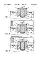
- FIG. 1 is a vertical sectional view of a first stage in the process of forming the flash memory structure of the present invention, after a vertical floating gate is formed.
- FIG. 2 is a vertical sectional view of a process stage subsequent to FIG. 1 in which the floating gate is split.
- FIG. 3 is a vertical sectional view of a process stage subsequent to FIG. 2 in which a vertical bit line is formed between the split floating gate.
- FIG. 4 is a vertical sectional view of a process stage subsequent to FIG. 3 in which an oxide is deposited over the vertical bit line and split floating gate.
- FIG. 5 is a vertical sectional view of a process stage subsequent to FIG. 4 in which a word line and insulator are deposited over the oxide, vertical bit line and split floating gate.
- FIG. 6 is a vertical sectional view of a process stage subsequent to FIG. 5 in which metal vias are formed in the flash memory structure.
- FIG. 7 is a top plan view of the various masks employed to form the structural elements shown in FIGS. 1-6 along line A--A.
- FIG. 8 is a perspective view of the flash memory structure formed by the process shown in FIGS. 1-6.
- FIG. 9 is a schematic of the flash memory structure of the present invention.
- FIGS. 1-9 of the drawings in which like numerals refer to like features of the invention.
- Features of the invention are not necessarily shown to scale in the drawings.
- FIGS. 1-7 The preferred process for producing the flash memory structure of the present invention is depicted in FIGS. 1-7.
- the single crystal silicon substrate 20 of a wafer has deposited thereon a thick gate silicon dioxide layer 21.
- the thickness of layer 21 is from about 200 to 300 angstroms.
- a second dielectric layer 23 of silicon nitride is deposited over the silicon oxide dielectric layer 21.
- the silicon nitride layer is then masked with a floating gate (FG) mask as shown in the top plan view of FIG. 7.
- FG floating gate
- Reactive ion etching is utilized to form a trench 40 extending below the surface of substrate 20.
- FG floating gate
- a thin gate silicon dioxide layer 22 is deposited to line the inner surfaces of trench 40.
- a polycrystalline silicon 31 is deposited to fill trench 40, and chemical mechanical polishing is utilized to make coplanar the upper surfaces of polysilicon filled 31 and nitride layer 23.
- a source implant (SI) mask as shown in FIG. 7 is deposited over nitride layer 23 to permit implanting of arsenic to form the source regions 28 spaced apart and on either side of the previously formed gate.
- a mask is then applied over the surface of the SI mask which exposes a portion of the surface of the polysilicon gate fill 31. Reactive ion etching is the used to create trench 42 which splits the floating gate into split floating gate portions 31a, 31b. The bottom of trench 42 may extend below the bottom of split floating gate portions 31a, 31b.
- the masks are stripped and there is formed a thin silicon nitride film on the walls of trench 42, which film is then oxidized and reactive ion etched to form the thin nitride spacer 25.
- an n-type dopant such as arsenic or phosphorous is implanted at the bottom of trench 42 to form drain region 27.
- Trench 42 is then filled with polysilicon to form a bit line 32, also known as the auxiliary gate. As shown, the lower portion of bit line 32 extends below the lowermost portions of split floating gate portions 31a, 31b.
- the structure is then again subject to chemical mechanical polishing to make the surface of nitride layer 23 and the bit line 32 and split floating gate portions 31a, 31b regions coplanar.
- a cap silicon oxide layer 24 is then grown over the bit line and split floating gate region, as shown in FIG. 4, and nitride layer 23 is stripped using a hot phosphorous stripping agent.
- a tunneling silicon dioxide layer 26 is then applied to the exposed vertical side surfaces of a floating gate portions 31a, 31b, above oxide layer 21. The uppermost portion of bit line 32 and split floating gate portions 31a, 31b extend above the surface of substrate 20 at substantially the same height.
- a polysilicon layer 33 is applied which, after masking with the word line (WL) mask as shown in FIG. 7 and reactive ion etching, forms the word line, also known as the control gate, for the flash memory structure.
- the WL mask is then stripped and the gate side walls are oxidized and a spacer nitride is then deposited and reactive ion etched.
- a layer of titanium salicide over the polycrystalline word line 33.
- an insulator 38 such as polysilicate glass (PSG) is deposited over the word line.
- a contact (CA) mask as shown in FIG. 7 is then applied and reactive ion etched to form vertical openings in which metal 52 is deposited to form a via.
- a metal mask is then applied and reactive ion etched to leave metal layers 51 (FIG. 6) in contact with the metal via 52 which contacts the control gate.
- the finished structure is shown in perspective view (with the insulator layer removed) in FIG. 8 wherein the source 28, floating gate 31a, 31b, bit line 32, drain 27 and oxide cap 24 extend along the X-direction of the structure while the word lines 33 extend thereover in the Y-direction in discreet sections.
- FIG. 9 A schematic of the flash memory structure of the present invention is shown in FIG. 9.
- a positive voltage of for example 8-10 volts is applied to the drain and bit line. This results in the ejection of hot electrons into the floating gate as indicated by arrow 60.
- the source is connected to ground and the word line (WL) is connected to a significantly lower voltage than the bit line, for example, approximately 1 volt.
- the source is connected to a ground potential
- the word line is connected to approximately 1 volt potential
- the bit line and drain are connected to approximately 1.5 volt potential.
- Erasing of the cell is done by applying positive voltage to the word line, e.g., 6 volts, to induce Fowler-Nordheim tunneling of electrons from the polysilicon floating gate (FG) to the polysilicon word line (WL) as shown by arrow 61 through the thin tunneling oxide layer (26 FIGS. 4-6). Accordingly, the present invention provides a EEPROM flash memory cell which has excellent operational parameters while having a considerably simpler structure which may be produced by a less complex process than the prior art.
Landscapes
- Engineering & Computer Science (AREA)
- Microelectronics & Electronic Packaging (AREA)
- Power Engineering (AREA)
- Physics & Mathematics (AREA)
- Ceramic Engineering (AREA)
- Condensed Matter Physics & Semiconductors (AREA)
- General Physics & Mathematics (AREA)
- Computer Hardware Design (AREA)
- Manufacturing & Machinery (AREA)
- Semiconductor Memories (AREA)
- Non-Volatile Memory (AREA)
Abstract
Description
Claims (12)
Priority Applications (1)
| Application Number | Priority Date | Filing Date | Title |
|---|---|---|---|
| US09/225,055 US6130453A (en) | 1999-01-04 | 1999-01-04 | Flash memory structure with floating gate in vertical trench |
Applications Claiming Priority (1)
| Application Number | Priority Date | Filing Date | Title |
|---|---|---|---|
| US09/225,055 US6130453A (en) | 1999-01-04 | 1999-01-04 | Flash memory structure with floating gate in vertical trench |
Publications (1)
| Publication Number | Publication Date |
|---|---|
| US6130453A true US6130453A (en) | 2000-10-10 |
Family
ID=22843335
Family Applications (1)
| Application Number | Title | Priority Date | Filing Date |
|---|---|---|---|
| US09/225,055 Expired - Lifetime US6130453A (en) | 1999-01-04 | 1999-01-04 | Flash memory structure with floating gate in vertical trench |
Country Status (1)
| Country | Link |
|---|---|
| US (1) | US6130453A (en) |
Cited By (67)
| Publication number | Priority date | Publication date | Assignee | Title |
|---|---|---|---|---|
| US20020100942A1 (en) * | 2000-12-04 | 2002-08-01 | Fitzgerald Eugene A. | CMOS inverter and integrated circuits utilizing strained silicon surface channel MOSFETs |
| US6465836B2 (en) | 2001-03-29 | 2002-10-15 | Taiwan Semiconductor Manufacturing Co., Ltd | Vertical split gate field effect transistor (FET) device |
| US6490196B1 (en) * | 2000-12-08 | 2002-12-03 | Ememory Technology Inc. | Method for operating a nonvolatile memory having embedded word lines |
| US20020197803A1 (en) * | 2001-06-21 | 2002-12-26 | Amberwave Systems Corporation | Enhancement of p-type metal-oxide-semiconductor field effect transistors |
| US20030013323A1 (en) * | 2001-06-14 | 2003-01-16 | Richard Hammond | Method of selective removal of SiGe alloys |
| US20030057439A1 (en) * | 2001-08-09 | 2003-03-27 | Fitzgerald Eugene A. | Dual layer CMOS devices |
| US6555839B2 (en) | 2000-05-26 | 2003-04-29 | Amberwave Systems Corporation | Buried channel strained silicon FET using a supply layer created through ion implantation |
| US6566194B1 (en) | 2001-10-01 | 2003-05-20 | Advanced Micro Devices, Inc. | Salicided gate for virtual ground arrays |
| US20030186506A1 (en) * | 2002-03-26 | 2003-10-02 | Nanya Technology Corporation | Split gate flash memory and formation method thereof |
| US6645801B1 (en) | 2001-10-01 | 2003-11-11 | Advanced Micro Devices, Inc. | Salicided gate for virtual ground arrays |
| US6649480B2 (en) | 2000-12-04 | 2003-11-18 | Amberwave Systems Corporation | Method of fabricating CMOS inverter and integrated circuits utilizing strained silicon surface channel MOSFETs |
| US20040026765A1 (en) * | 2002-06-07 | 2004-02-12 | Amberwave Systems Corporation | Semiconductor devices having strained dual channel layers |
| US6703688B1 (en) | 2001-03-02 | 2004-03-09 | Amberwave Systems Corporation | Relaxed silicon germanium platform for high speed CMOS electronics and high speed analog circuits |
| US6703144B2 (en) | 2000-01-20 | 2004-03-09 | Amberwave Systems Corporation | Heterointegration of materials using deposition and bonding |
| US6713326B2 (en) | 2000-08-16 | 2004-03-30 | Masachusetts Institute Of Technology | Process for producing semiconductor article using graded epitaxial growth |
| US6723661B2 (en) | 2001-03-02 | 2004-04-20 | Amberwave Systems Corporation | Relaxed silicon germanium platform for high speed CMOS electronics and high speed analog circuits |
| US6724008B2 (en) | 2001-03-02 | 2004-04-20 | Amberwave Systems Corporation | Relaxed silicon germanium platform for high speed CMOS electronics and high speed analog circuits |
| US6730564B1 (en) | 2002-08-12 | 2004-05-04 | Fasl, Llc | Salicided gate for virtual ground arrays |
| US6730551B2 (en) | 2001-08-06 | 2004-05-04 | Massachusetts Institute Of Technology | Formation of planar strained layers |
| WO2004057661A2 (en) * | 2002-12-19 | 2004-07-08 | Koninklijke Philips Electronics N.V. | Non-volatile memory cell and method of fabrication |
| US20040183118A1 (en) * | 2003-03-21 | 2004-09-23 | Silicon Storage Technology, Inc. | Semiconductor memory array of floating gate memory cells with burried floating gate and pointed channel region |
| US20040197996A1 (en) * | 2003-03-21 | 2004-10-07 | Bomy Chen | Self aligned method of forming a semiconductor memory array of floating gate memory cells with buried floating gate, pointed floating gate and pointed channel region, and a memory array made thereby |
| US20040207039A1 (en) * | 2001-06-29 | 2004-10-21 | Kabushiki Kaisha Toshiba | Semiconductor device and method of manufacturing a semiconductor device |
| US20050023603A1 (en) * | 2001-08-30 | 2005-02-03 | Micron Technology, Inc. | Atomic layer deposition of metal oxide and/or low asymmetrical tunnel barrier interpoly insulators |
| US6864115B2 (en) | 2000-01-20 | 2005-03-08 | Amberwave Systems Corporation | Low threading dislocation density relaxed mismatched epilayers without high temperature growth |
| US6876010B1 (en) | 1997-06-24 | 2005-04-05 | Massachusetts Institute Of Technology | Controlling threading dislocation densities in Ge on Si using graded GeSi layers and planarization |
| US20050139910A1 (en) * | 2003-12-30 | 2005-06-30 | Koh Kwan J. | Semiconductor devices and methods for fabricating the same |
| US6933518B2 (en) | 2001-09-24 | 2005-08-23 | Amberwave Systems Corporation | RF circuits including transistors having strained material layers |
| US6940089B2 (en) | 2001-04-04 | 2005-09-06 | Massachusetts Institute Of Technology | Semiconductor device structure |
| US20050205922A1 (en) * | 2004-03-18 | 2005-09-22 | Yuan-Hung Liu | Flash memory cell and methods for fabricating same |
| US20050250335A1 (en) * | 2004-05-07 | 2005-11-10 | Min-San Huang | [method of fabricating flash memory cell] |
| US6995430B2 (en) | 2002-06-07 | 2006-02-07 | Amberwave Systems Corporation | Strained-semiconductor-on-insulator device structures |
| US20060043459A1 (en) * | 2004-09-02 | 2006-03-02 | Bomy Chen | Non-planar non-volatile memory cell with an erase gate, an array therefor, and a method of making same |
| US20060113603A1 (en) * | 2004-12-01 | 2006-06-01 | Amberwave Systems Corporation | Hybrid semiconductor-on-insulator structures and related methods |
| US7060632B2 (en) | 2002-03-14 | 2006-06-13 | Amberwave Systems Corporation | Methods for fabricating strained layers on semiconductor substrates |
| US20060146640A1 (en) * | 2004-12-31 | 2006-07-06 | Dongbuanam Semiconductor Inc. | Memory device and method for manufacturing the same |
| US7074623B2 (en) | 2002-06-07 | 2006-07-11 | Amberwave Systems Corporation | Methods of forming strained-semiconductor-on-insulator finFET device structures |
| US20060189074A1 (en) * | 2005-02-18 | 2006-08-24 | Hann-Jye Hsu | Structure containing self-aligned conductive lines and fabricating method thereof |
| US20060186458A1 (en) * | 2005-02-23 | 2006-08-24 | Micron Technology,Inc. | Germanium-silicon-carbide floating gates in memories |
| US20060211204A1 (en) * | 2005-03-18 | 2006-09-21 | Min-San Huang | Non-volatile memory and method of fabricating the same |
| US7138649B2 (en) | 2001-08-09 | 2006-11-21 | Amberwave Systems Corporation | Dual-channel CMOS transistors with differentially strained channels |
| CN1307710C (en) * | 2004-03-26 | 2007-03-28 | 力晶半导体股份有限公司 | Method for producing flash memory storing unit |
| US20070082470A1 (en) * | 2000-08-07 | 2007-04-12 | Amberwave System Corporation | Gate technology for strained surface channel and strained buried channel MOSFET devices |
| US7227176B2 (en) | 1998-04-10 | 2007-06-05 | Massachusetts Institute Of Technology | Etch stop layer system |
| US20070195596A1 (en) * | 1999-07-14 | 2007-08-23 | Takashi Kobayashi | Semiconductor integrated circuit device, production and operation method thereof |
| US20070215931A1 (en) * | 2004-10-12 | 2007-09-20 | Sohrab Kianian | Non-volatile memory cell in a trench having a first portion deeper than a second portion, an array of such memory cells, and method of manufacturing |
| US20070262415A1 (en) * | 2006-05-11 | 2007-11-15 | Casey Smith | Recessed antifuse structures and methods of making the same |
| US20070264771A1 (en) * | 2006-05-11 | 2007-11-15 | Venkatesan Ananthan | Dual work function recessed access device and methods of forming |
| US20070262395A1 (en) * | 2006-05-11 | 2007-11-15 | Gibbons Jasper S | Memory cell access devices and methods of making the same |
| US7301180B2 (en) | 2001-06-18 | 2007-11-27 | Massachusetts Institute Of Technology | Structure and method for a high-speed semiconductor device having a Ge channel layer |
| US7307273B2 (en) | 2002-06-07 | 2007-12-11 | Amberwave Systems Corporation | Control of strain in device layers by selective relaxation |
| US7332417B2 (en) | 2003-01-27 | 2008-02-19 | Amberwave Systems Corporation | Semiconductor structures with structural homogeneity |
| US7335545B2 (en) | 2002-06-07 | 2008-02-26 | Amberwave Systems Corporation | Control of strain in device layers by prevention of relaxation |
| US7368308B2 (en) | 2002-08-23 | 2008-05-06 | Amberwave Systems Corporation | Methods of fabricating semiconductor heterostructures |
| US20080108212A1 (en) * | 2006-10-19 | 2008-05-08 | Atmel Corporation | High voltage vertically oriented eeprom device |
| US7372097B2 (en) | 2001-08-30 | 2008-05-13 | Micron Technology, Inc. | Programmable array logic or memory with p-channel devices and asymmetrical tunnel barriers |
| US7393733B2 (en) | 2004-12-01 | 2008-07-01 | Amberwave Systems Corporation | Methods of forming hybrid fin field-effect transistor structures |
| US7443715B2 (en) | 2001-08-30 | 2008-10-28 | Micron Technology, Inc. | SRAM cells with repressed floating gate memory, low tunnel barrier interpoly insulators |
| US20080303067A1 (en) * | 2007-06-07 | 2008-12-11 | Rao Rajesh A | Split gate memory cell using sidewall spacers |
| US7545674B2 (en) | 2001-08-30 | 2009-06-09 | Micron Technology, Inc. | Flash memory with low tunnel barrier interpoly insulators |
| US7572695B2 (en) | 2005-05-27 | 2009-08-11 | Micron Technology, Inc. | Hafnium titanium oxide films |
| US7594967B2 (en) | 2002-08-30 | 2009-09-29 | Amberwave Systems Corporation | Reduction of dislocation pile-up formation during relaxed lattice-mismatched epitaxy |
| US7776697B2 (en) | 2001-09-21 | 2010-08-17 | Taiwan Semiconductor Manufacturing Company, Ltd. | Semiconductor structures employing strained material layers with defined impurity gradients and methods for fabricating same |
| US7824986B2 (en) | 2008-11-05 | 2010-11-02 | Micron Technology, Inc. | Methods of forming a plurality of transistor gates, and methods of forming a plurality of transistor gates having at least two different work functions |
| US8129821B2 (en) | 2002-06-25 | 2012-03-06 | Taiwan Semiconductor Manufacturing Co., Ltd. | Reacted conductive gate electrodes |
| US8748292B2 (en) | 2002-06-07 | 2014-06-10 | Taiwan Semiconductor Manufacturing Company, Ltd. | Methods of forming strained-semiconductor-on-insulator device structures |
| US8822282B2 (en) | 2001-03-02 | 2014-09-02 | Taiwan Semiconductor Manufacturing Company, Ltd. | Methods of fabricating contact regions for FET incorporating SiGe |
Citations (10)
| Publication number | Priority date | Publication date | Assignee | Title |
|---|---|---|---|---|
| US4929988A (en) * | 1987-08-25 | 1990-05-29 | Kabushiki Kaisha Toshiba | Non-volatile semiconductor memory device and method of the manufacture thereof |
| US5386132A (en) * | 1992-11-02 | 1995-01-31 | Wong; Chun C. D. | Multimedia storage system with highly compact memory device |
| US5479368A (en) * | 1993-09-30 | 1995-12-26 | Cirrus Logic, Inc. | Spacer flash cell device with vertically oriented floating gate |
| US5492846A (en) * | 1993-11-01 | 1996-02-20 | Nec Corporation | Fabrication method of nonvolatile semiconductor memory device |
| US5495441A (en) * | 1994-05-18 | 1996-02-27 | United Microelectronics Corporation | Split-gate flash memory cell |
| US5512505A (en) * | 1990-12-18 | 1996-04-30 | Sandisk Corporation | Method of making dense vertical programmable read only memory cell structure |
| US5617351A (en) * | 1992-03-12 | 1997-04-01 | International Business Machines Corporation | Three-dimensional direct-write EEPROM arrays and fabrication methods |
| US5640031A (en) * | 1993-09-30 | 1997-06-17 | Keshtbod; Parviz | Spacer flash cell process |
| US5656544A (en) * | 1992-03-12 | 1997-08-12 | International Business Machines Corporation | Process for forming a polysilicon electrode in a trench |
| US5680345A (en) * | 1995-06-06 | 1997-10-21 | Advanced Micro Devices, Inc. | Nonvolatile memory cell with vertical gate overlap and zero birds beaks |
-
1999
- 1999-01-04 US US09/225,055 patent/US6130453A/en not_active Expired - Lifetime
Patent Citations (10)
| Publication number | Priority date | Publication date | Assignee | Title |
|---|---|---|---|---|
| US4929988A (en) * | 1987-08-25 | 1990-05-29 | Kabushiki Kaisha Toshiba | Non-volatile semiconductor memory device and method of the manufacture thereof |
| US5512505A (en) * | 1990-12-18 | 1996-04-30 | Sandisk Corporation | Method of making dense vertical programmable read only memory cell structure |
| US5617351A (en) * | 1992-03-12 | 1997-04-01 | International Business Machines Corporation | Three-dimensional direct-write EEPROM arrays and fabrication methods |
| US5656544A (en) * | 1992-03-12 | 1997-08-12 | International Business Machines Corporation | Process for forming a polysilicon electrode in a trench |
| US5386132A (en) * | 1992-11-02 | 1995-01-31 | Wong; Chun C. D. | Multimedia storage system with highly compact memory device |
| US5479368A (en) * | 1993-09-30 | 1995-12-26 | Cirrus Logic, Inc. | Spacer flash cell device with vertically oriented floating gate |
| US5640031A (en) * | 1993-09-30 | 1997-06-17 | Keshtbod; Parviz | Spacer flash cell process |
| US5492846A (en) * | 1993-11-01 | 1996-02-20 | Nec Corporation | Fabrication method of nonvolatile semiconductor memory device |
| US5495441A (en) * | 1994-05-18 | 1996-02-27 | United Microelectronics Corporation | Split-gate flash memory cell |
| US5680345A (en) * | 1995-06-06 | 1997-10-21 | Advanced Micro Devices, Inc. | Nonvolatile memory cell with vertical gate overlap and zero birds beaks |
Non-Patent Citations (4)
| Title |
|---|
| Ma, Y; Pang, C.S.; Pathak, J.; Tsao, S.C. and Chang, C.F. A Novel High Density Contactless Flash Memory Array Using Split Gate Source Side Injection Cell for SV Only Applications 1994 Symposium of VLSI Technology Digest of Technical Papers VLSI Research Laboratory, Sharp Corporation, 1994 IEEE, pp. 49 50. * |
| Ma, Y; Pang, C.S.; Pathak, J.; Tsao, S.C. and Chang, C.F.--A Novel High Density Contactless Flash Memory Array Using Split-Gate Source-Side-Injection Cell for SV-Only Applications--1994 Symposium of VLSI Technology Digest of Technical Papers--VLSI Research Laboratory, Sharp Corporation, 1994 IEEE, pp. 49-50. |
| Yamauchi, Yoshimitsu; Tanaka, Kenichi; Shibayama, Hikou; Miyaka, Ryuichiro A 5V Only Virtual Ground Flash Cell With an Auxiliary Gate for High Density and High Speed Application VLSI Research Laboratory, Sharp Corporation 1991 IEEE, pp. 11.7.1 11.7.4. * |
| Yamauchi, Yoshimitsu; Tanaka, Kenichi; Shibayama, Hikou; Miyaka, Ryuichiro--A 5V-Only Virtual Ground Flash Cell With an Auxiliary Gate for High Density and High Speed Application--VLSI Research Laboratory, Sharp Corporation 1991 IEEE, pp. 11.7.1-11.7.4. |
Cited By (138)
| Publication number | Priority date | Publication date | Assignee | Title |
|---|---|---|---|---|
| US7081410B2 (en) | 1997-06-24 | 2006-07-25 | Massachusetts Institute Of Technology | Controlling threading dislocation densities in Ge on Si using graded GeSi layers and planarization |
| US6876010B1 (en) | 1997-06-24 | 2005-04-05 | Massachusetts Institute Of Technology | Controlling threading dislocation densities in Ge on Si using graded GeSi layers and planarization |
| US7250359B2 (en) | 1997-06-24 | 2007-07-31 | Massachusetts Institute Of Technology | Controlling threading dislocation densities in Ge on Si using graded GeSi layers and planarization |
| US7227176B2 (en) | 1998-04-10 | 2007-06-05 | Massachusetts Institute Of Technology | Etch stop layer system |
| US20070195596A1 (en) * | 1999-07-14 | 2007-08-23 | Takashi Kobayashi | Semiconductor integrated circuit device, production and operation method thereof |
| US7366015B2 (en) * | 1999-07-14 | 2008-04-29 | Renesas Technology Corp. | Semiconductor integrated circuit device, production and operation method thereof |
| US6703144B2 (en) | 2000-01-20 | 2004-03-09 | Amberwave Systems Corporation | Heterointegration of materials using deposition and bonding |
| US6864115B2 (en) | 2000-01-20 | 2005-03-08 | Amberwave Systems Corporation | Low threading dislocation density relaxed mismatched epilayers without high temperature growth |
| US6555839B2 (en) | 2000-05-26 | 2003-04-29 | Amberwave Systems Corporation | Buried channel strained silicon FET using a supply layer created through ion implantation |
| US20070082470A1 (en) * | 2000-08-07 | 2007-04-12 | Amberwave System Corporation | Gate technology for strained surface channel and strained buried channel MOSFET devices |
| US6737670B2 (en) | 2000-08-16 | 2004-05-18 | Massachusetts Institute Of Technology | Semiconductor substrate structure |
| US6713326B2 (en) | 2000-08-16 | 2004-03-30 | Masachusetts Institute Of Technology | Process for producing semiconductor article using graded epitaxial growth |
| US6921914B2 (en) | 2000-08-16 | 2005-07-26 | Massachusetts Institute Of Technology | Process for producing semiconductor article using graded epitaxial growth |
| US6649480B2 (en) | 2000-12-04 | 2003-11-18 | Amberwave Systems Corporation | Method of fabricating CMOS inverter and integrated circuits utilizing strained silicon surface channel MOSFETs |
| US20020100942A1 (en) * | 2000-12-04 | 2002-08-01 | Fitzgerald Eugene A. | CMOS inverter and integrated circuits utilizing strained silicon surface channel MOSFETs |
| US6881632B2 (en) | 2000-12-04 | 2005-04-19 | Amberwave Systems Corporation | Method of fabricating CMOS inverter and integrated circuits utilizing strained surface channel MOSFETS |
| US6490196B1 (en) * | 2000-12-08 | 2002-12-03 | Ememory Technology Inc. | Method for operating a nonvolatile memory having embedded word lines |
| US6703688B1 (en) | 2001-03-02 | 2004-03-09 | Amberwave Systems Corporation | Relaxed silicon germanium platform for high speed CMOS electronics and high speed analog circuits |
| US6723661B2 (en) | 2001-03-02 | 2004-04-20 | Amberwave Systems Corporation | Relaxed silicon germanium platform for high speed CMOS electronics and high speed analog circuits |
| US6724008B2 (en) | 2001-03-02 | 2004-04-20 | Amberwave Systems Corporation | Relaxed silicon germanium platform for high speed CMOS electronics and high speed analog circuits |
| US8822282B2 (en) | 2001-03-02 | 2014-09-02 | Taiwan Semiconductor Manufacturing Company, Ltd. | Methods of fabricating contact regions for FET incorporating SiGe |
| US6465836B2 (en) | 2001-03-29 | 2002-10-15 | Taiwan Semiconductor Manufacturing Co., Ltd | Vertical split gate field effect transistor (FET) device |
| US6940089B2 (en) | 2001-04-04 | 2005-09-06 | Massachusetts Institute Of Technology | Semiconductor device structure |
| US7348259B2 (en) | 2001-04-04 | 2008-03-25 | Massachusetts Institute Of Technology | Method of fabricating a semiconductor structure that includes transferring one or more material layers to a substrate and smoothing an exposed surface of at least one of the material layers |
| US20040171223A1 (en) * | 2001-06-14 | 2004-09-02 | Amberwave Systems Corporation | Method of selective removal of SiGe alloys |
| US20030013323A1 (en) * | 2001-06-14 | 2003-01-16 | Richard Hammond | Method of selective removal of SiGe alloys |
| US6900094B2 (en) | 2001-06-14 | 2005-05-31 | Amberwave Systems Corporation | Method of selective removal of SiGe alloys |
| US7301180B2 (en) | 2001-06-18 | 2007-11-27 | Massachusetts Institute Of Technology | Structure and method for a high-speed semiconductor device having a Ge channel layer |
| US8436336B2 (en) | 2001-06-18 | 2013-05-07 | Massachusetts Institute Of Technology | Structure and method for a high-speed semiconductor device having a Ge channel layer |
| US6916727B2 (en) | 2001-06-21 | 2005-07-12 | Massachusetts Institute Of Technology | Enhancement of P-type metal-oxide-semiconductor field effect transistors |
| US20050151164A1 (en) * | 2001-06-21 | 2005-07-14 | Amberwave Systems Corporation | Enhancement of p-type metal-oxide-semiconductor field effect transistors |
| US20020197803A1 (en) * | 2001-06-21 | 2002-12-26 | Amberwave Systems Corporation | Enhancement of p-type metal-oxide-semiconductor field effect transistors |
| US20060244098A1 (en) * | 2001-06-29 | 2006-11-02 | Kabushiki Kaisha Toshiba | Semiconductor device and method of manufacturing a semiconductor device |
| US20040207039A1 (en) * | 2001-06-29 | 2004-10-21 | Kabushiki Kaisha Toshiba | Semiconductor device and method of manufacturing a semiconductor device |
| US7095093B2 (en) | 2001-06-29 | 2006-08-22 | Kabushiki Kaisha Toshiba | Semiconductor device and method of manufacturing a semiconductor device |
| US7141820B2 (en) | 2001-08-06 | 2006-11-28 | Amberwave Systems Corporation | Structures with planar strained layers |
| US20040164318A1 (en) * | 2001-08-06 | 2004-08-26 | Massachusetts Institute Of Technology | Structures with planar strained layers |
| US6730551B2 (en) | 2001-08-06 | 2004-05-04 | Massachusetts Institute Of Technology | Formation of planar strained layers |
| US7138649B2 (en) | 2001-08-09 | 2006-11-21 | Amberwave Systems Corporation | Dual-channel CMOS transistors with differentially strained channels |
| US7465619B2 (en) | 2001-08-09 | 2008-12-16 | Amberwave Systems Corporation | Methods of fabricating dual layer semiconductor devices |
| US20030057439A1 (en) * | 2001-08-09 | 2003-03-27 | Fitzgerald Eugene A. | Dual layer CMOS devices |
| US20050221550A1 (en) * | 2001-08-09 | 2005-10-06 | Amberwave Systems Corporation | Dual layer semiconductor devices |
| US6974735B2 (en) | 2001-08-09 | 2005-12-13 | Amberwave Systems Corporation | Dual layer Semiconductor Devices |
| US7508025B2 (en) | 2001-08-30 | 2009-03-24 | Micron Technology, Inc. | Atomic layer deposition of metal oxide and/or low asymmetrical tunnel barrier interpoly insulators |
| US7391072B2 (en) | 2001-08-30 | 2008-06-24 | Micron Technology, Inc. | Programmable array logic or memory with p-channel devices and asymmetrical tunnel barriers |
| US7372097B2 (en) | 2001-08-30 | 2008-05-13 | Micron Technology, Inc. | Programmable array logic or memory with p-channel devices and asymmetrical tunnel barriers |
| US7372096B2 (en) | 2001-08-30 | 2008-05-13 | Micron Technology, Inc. | Programmable array logic or memory with p-channel devices and asymmetrical tunnel barriers |
| US7443715B2 (en) | 2001-08-30 | 2008-10-28 | Micron Technology, Inc. | SRAM cells with repressed floating gate memory, low tunnel barrier interpoly insulators |
| US7465983B2 (en) | 2001-08-30 | 2008-12-16 | Micron Technology, Inc. | Low tunnel barrier insulators |
| US7473956B2 (en) | 2001-08-30 | 2009-01-06 | Micron Technology, Inc. | Atomic layer deposition of metal oxide and/or low assymmetrical tunnel barrier interpoly insulators |
| US7504687B2 (en) | 2001-08-30 | 2009-03-17 | Micron Technology, Inc. | Atomic layer deposition of metal oxide and/or low asymmetrical tunnel barrier interpoly insulators |
| US20050023603A1 (en) * | 2001-08-30 | 2005-02-03 | Micron Technology, Inc. | Atomic layer deposition of metal oxide and/or low asymmetrical tunnel barrier interpoly insulators |
| US7545674B2 (en) | 2001-08-30 | 2009-06-09 | Micron Technology, Inc. | Flash memory with low tunnel barrier interpoly insulators |
| US7759724B2 (en) | 2001-08-30 | 2010-07-20 | Micron Technology, Inc. | Memory cells having gate structure with multiple gates and multiple materials between the gates |
| US7776697B2 (en) | 2001-09-21 | 2010-08-17 | Taiwan Semiconductor Manufacturing Company, Ltd. | Semiconductor structures employing strained material layers with defined impurity gradients and methods for fabricating same |
| US7846802B2 (en) | 2001-09-21 | 2010-12-07 | Taiwan Semiconductor Manufacturing Company, Ltd. | Semiconductor structures employing strained material layers with defined impurity gradients and methods for fabricating same |
| US7884353B2 (en) | 2001-09-21 | 2011-02-08 | Taiwan Semiconductor Manufacturing Company, Ltd. | Semiconductor structures employing strained material layers with defined impurity gradients and methods for fabricating same |
| US7906776B2 (en) | 2001-09-24 | 2011-03-15 | Taiwan Semiconductor Manufacturing Company, Ltd. | RF circuits including transistors having strained material layers |
| US7709828B2 (en) | 2001-09-24 | 2010-05-04 | Taiwan Semiconductor Manufacturing Company, Ltd. | RF circuits including transistors having strained material layers |
| US6933518B2 (en) | 2001-09-24 | 2005-08-23 | Amberwave Systems Corporation | RF circuits including transistors having strained material layers |
| US6566194B1 (en) | 2001-10-01 | 2003-05-20 | Advanced Micro Devices, Inc. | Salicided gate for virtual ground arrays |
| US6645801B1 (en) | 2001-10-01 | 2003-11-11 | Advanced Micro Devices, Inc. | Salicided gate for virtual ground arrays |
| US7259108B2 (en) | 2002-03-14 | 2007-08-21 | Amberwave Systems Corporation | Methods for fabricating strained layers on semiconductor substrates |
| US7060632B2 (en) | 2002-03-14 | 2006-06-13 | Amberwave Systems Corporation | Methods for fabricating strained layers on semiconductor substrates |
| US20030186506A1 (en) * | 2002-03-26 | 2003-10-02 | Nanya Technology Corporation | Split gate flash memory and formation method thereof |
| US6720219B2 (en) * | 2002-03-26 | 2004-04-13 | Nanya Technology Corporation | Split gate flash memory and formation method thereof |
| US20040026765A1 (en) * | 2002-06-07 | 2004-02-12 | Amberwave Systems Corporation | Semiconductor devices having strained dual channel layers |
| US7109516B2 (en) | 2002-06-07 | 2006-09-19 | Amberwave Systems Corporation | Strained-semiconductor-on-insulator finFET device structures |
| US6995430B2 (en) | 2002-06-07 | 2006-02-07 | Amberwave Systems Corporation | Strained-semiconductor-on-insulator device structures |
| US7566606B2 (en) | 2002-06-07 | 2009-07-28 | Amberwave Systems Corporation | Methods of fabricating semiconductor devices having strained dual channel layers |
| US7074623B2 (en) | 2002-06-07 | 2006-07-11 | Amberwave Systems Corporation | Methods of forming strained-semiconductor-on-insulator finFET device structures |
| US7297612B2 (en) | 2002-06-07 | 2007-11-20 | Amberwave Systems Corporation | Methods for forming strained-semiconductor-on-insulator device structures by use of cleave planes |
| US8748292B2 (en) | 2002-06-07 | 2014-06-10 | Taiwan Semiconductor Manufacturing Company, Ltd. | Methods of forming strained-semiconductor-on-insulator device structures |
| US7307273B2 (en) | 2002-06-07 | 2007-12-11 | Amberwave Systems Corporation | Control of strain in device layers by selective relaxation |
| US7259388B2 (en) | 2002-06-07 | 2007-08-21 | Amberwave Systems Corporation | Strained-semiconductor-on-insulator device structures |
| US7138310B2 (en) | 2002-06-07 | 2006-11-21 | Amberwave Systems Corporation | Semiconductor devices having strained dual channel layers |
| US7838392B2 (en) | 2002-06-07 | 2010-11-23 | Taiwan Semiconductor Manufacturing Company, Ltd. | Methods for forming III-V semiconductor device structures |
| US7335545B2 (en) | 2002-06-07 | 2008-02-26 | Amberwave Systems Corporation | Control of strain in device layers by prevention of relaxation |
| US8129821B2 (en) | 2002-06-25 | 2012-03-06 | Taiwan Semiconductor Manufacturing Co., Ltd. | Reacted conductive gate electrodes |
| US6730564B1 (en) | 2002-08-12 | 2004-05-04 | Fasl, Llc | Salicided gate for virtual ground arrays |
| US7368308B2 (en) | 2002-08-23 | 2008-05-06 | Amberwave Systems Corporation | Methods of fabricating semiconductor heterostructures |
| US7829442B2 (en) | 2002-08-23 | 2010-11-09 | Taiwan Semiconductor Manufacturing Company, Ltd. | Semiconductor heterostructures having reduced dislocation pile-ups and related methods |
| US7375385B2 (en) | 2002-08-23 | 2008-05-20 | Amberwave Systems Corporation | Semiconductor heterostructures having reduced dislocation pile-ups |
| US7594967B2 (en) | 2002-08-30 | 2009-09-29 | Amberwave Systems Corporation | Reduction of dislocation pile-up formation during relaxed lattice-mismatched epitaxy |
| WO2004057661A3 (en) * | 2002-12-19 | 2004-09-02 | Koninkl Philips Electronics Nv | Non-volatile memory cell and method of fabrication |
| WO2004057661A2 (en) * | 2002-12-19 | 2004-07-08 | Koninklijke Philips Electronics N.V. | Non-volatile memory cell and method of fabrication |
| US20060220093A1 (en) * | 2002-12-19 | 2006-10-05 | Koninklijke Philips Electronics N.V. | Non-volatile memory cell and method of fabrication |
| US7332417B2 (en) | 2003-01-27 | 2008-02-19 | Amberwave Systems Corporation | Semiconductor structures with structural homogeneity |
| US6873006B2 (en) * | 2003-03-21 | 2005-03-29 | Silicon Storage Technology, Inc. | Semiconductor memory array of floating gate memory cells with burried floating gate and pointed channel region |
| US7180127B2 (en) * | 2003-03-21 | 2007-02-20 | Silicon Storage Technology, Inc. | Semiconductor memory array of floating gate memory cells with buried floating gate, pointed floating gate and pointed channel region |
| US20040183118A1 (en) * | 2003-03-21 | 2004-09-23 | Silicon Storage Technology, Inc. | Semiconductor memory array of floating gate memory cells with burried floating gate and pointed channel region |
| US20040197996A1 (en) * | 2003-03-21 | 2004-10-07 | Bomy Chen | Self aligned method of forming a semiconductor memory array of floating gate memory cells with buried floating gate, pointed floating gate and pointed channel region, and a memory array made thereby |
| CN100382321C (en) * | 2003-03-21 | 2008-04-16 | 硅存储技术公司 | Semiconductor memory matrix of flating gate memory unit |
| US20050199914A1 (en) * | 2003-03-21 | 2005-09-15 | Bomy Chen | Self aligned method of forming a semiconductor memory array of floating gate memory cells with buried floating gate and pointed channel region |
| US7208376B2 (en) | 2003-03-21 | 2007-04-24 | Silicon Storage Technology, Inc. | Self aligned method of forming a semiconductor memory array of floating gate memory cells with buried floating gate and pointed channel region |
| US20040238874A1 (en) * | 2003-03-21 | 2004-12-02 | Bomy Chen | Semiconductor memory array of floating gate memory cells with buried floating gate, pointed floating gate and pointed channel region |
| US6958273B2 (en) | 2003-03-21 | 2005-10-25 | Silicon Storage Technology, Inc. | Self-aligned method of forming a semiconductor memory array of floating gate memory cells with buried floating gate, pointed floating gate and pointed channel region, and a memory array made thereby |
| US20050139910A1 (en) * | 2003-12-30 | 2005-06-30 | Koh Kwan J. | Semiconductor devices and methods for fabricating the same |
| US7183609B2 (en) * | 2003-12-30 | 2007-02-27 | Dongbu Electronics Co., Ltd. | Semiconductor devices and methods for fabricating the same |
| US20050205922A1 (en) * | 2004-03-18 | 2005-09-22 | Yuan-Hung Liu | Flash memory cell and methods for fabricating same |
| US7214589B2 (en) * | 2004-03-18 | 2007-05-08 | Taiwan Semiconductor Manufacturing Co., Ltd. | Flash memory cell and methods for fabricating same |
| CN1307710C (en) * | 2004-03-26 | 2007-03-28 | 力晶半导体股份有限公司 | Method for producing flash memory storing unit |
| US6972260B2 (en) * | 2004-05-07 | 2005-12-06 | Powerchip Semiconductor Corp. | Method of fabricating flash memory cell |
| US20050250335A1 (en) * | 2004-05-07 | 2005-11-10 | Min-San Huang | [method of fabricating flash memory cell] |
| US7129536B2 (en) * | 2004-09-02 | 2006-10-31 | Silicon Storage Technology, Inc. | Non-planar non-volatile memory cell with an erase gate, an array therefor, and a method of making same |
| US20060043459A1 (en) * | 2004-09-02 | 2006-03-02 | Bomy Chen | Non-planar non-volatile memory cell with an erase gate, an array therefor, and a method of making same |
| US20070215931A1 (en) * | 2004-10-12 | 2007-09-20 | Sohrab Kianian | Non-volatile memory cell in a trench having a first portion deeper than a second portion, an array of such memory cells, and method of manufacturing |
| US8183627B2 (en) | 2004-12-01 | 2012-05-22 | Taiwan Semiconductor Manufacturing Company, Ltd. | Hybrid fin field-effect transistor structures and related methods |
| US20060113603A1 (en) * | 2004-12-01 | 2006-06-01 | Amberwave Systems Corporation | Hybrid semiconductor-on-insulator structures and related methods |
| US7393733B2 (en) | 2004-12-01 | 2008-07-01 | Amberwave Systems Corporation | Methods of forming hybrid fin field-effect transistor structures |
| US20090317952A1 (en) * | 2004-12-31 | 2009-12-24 | Heung Jin Kim | Memory Device and Method for Manufacturing the Same |
| US20090317953A1 (en) * | 2004-12-31 | 2009-12-24 | Heung Jin Kim | Memory Device and Method for Manufacturing the Same |
| US7923326B2 (en) | 2004-12-31 | 2011-04-12 | Dongbu Electronics Co., Ltd. | Memory device and method for manufacturing the same |
| US7598563B2 (en) | 2004-12-31 | 2009-10-06 | Dongbu Electronics Co., Ltd. | Memory device and method for manufacturing the same |
| US7883966B2 (en) | 2004-12-31 | 2011-02-08 | Dongbu Electronics Co., Ltd. | Memory device and method for manufacturing the same |
| US20060146640A1 (en) * | 2004-12-31 | 2006-07-06 | Dongbuanam Semiconductor Inc. | Memory device and method for manufacturing the same |
| US20060189074A1 (en) * | 2005-02-18 | 2006-08-24 | Hann-Jye Hsu | Structure containing self-aligned conductive lines and fabricating method thereof |
| US8330202B2 (en) | 2005-02-23 | 2012-12-11 | Micron Technology, Inc. | Germanium-silicon-carbide floating gates in memories |
| US20060186458A1 (en) * | 2005-02-23 | 2006-08-24 | Micron Technology,Inc. | Germanium-silicon-carbide floating gates in memories |
| US20060211204A1 (en) * | 2005-03-18 | 2006-09-21 | Min-San Huang | Non-volatile memory and method of fabricating the same |
| US7572695B2 (en) | 2005-05-27 | 2009-08-11 | Micron Technology, Inc. | Hafnium titanium oxide films |
| US7700989B2 (en) | 2005-05-27 | 2010-04-20 | Micron Technology, Inc. | Hafnium titanium oxide films |
| US8710583B2 (en) | 2006-05-11 | 2014-04-29 | Micron Technology, Inc. | Dual work function recessed access device and methods of forming |
| US20070262415A1 (en) * | 2006-05-11 | 2007-11-15 | Casey Smith | Recessed antifuse structures and methods of making the same |
| US8008144B2 (en) | 2006-05-11 | 2011-08-30 | Micron Technology, Inc. | Dual work function recessed access device and methods of forming |
| US9543433B2 (en) | 2006-05-11 | 2017-01-10 | Micron Technology, Inc. | Dual work function recessed access device and methods of forming |
| US9502516B2 (en) | 2006-05-11 | 2016-11-22 | Micron Technology, Inc. | Recessed access devices and gate electrodes |
| US8860174B2 (en) | 2006-05-11 | 2014-10-14 | Micron Technology, Inc. | Recessed antifuse structures and methods of making the same |
| US20070262395A1 (en) * | 2006-05-11 | 2007-11-15 | Gibbons Jasper S | Memory cell access devices and methods of making the same |
| US20070264771A1 (en) * | 2006-05-11 | 2007-11-15 | Venkatesan Ananthan | Dual work function recessed access device and methods of forming |
| US8692320B2 (en) | 2006-05-11 | 2014-04-08 | Micron Technology, Inc. | Recessed memory cell access devices and gate electrodes |
| US20080108212A1 (en) * | 2006-10-19 | 2008-05-08 | Atmel Corporation | High voltage vertically oriented eeprom device |
| US7704830B2 (en) * | 2007-06-07 | 2010-04-27 | Freescale Semiconductor, Inc. | Split gate memory cell using sidewall spacers |
| US20080303067A1 (en) * | 2007-06-07 | 2008-12-11 | Rao Rajesh A | Split gate memory cell using sidewall spacers |
| US20110039404A1 (en) * | 2008-11-05 | 2011-02-17 | Micron Technology, Inc. | Methods of Forming a Plurality of Transistor Gates, and Methods of Forming a Plurality of Transistor Gates Having at Least Two Different Work Functions |
| US8524561B2 (en) | 2008-11-05 | 2013-09-03 | Micron Technology, Inc. | Methods of forming a plurality of transistor gates, and methods of forming a plurality of transistor gates having at least two different work functions |
| US7824986B2 (en) | 2008-11-05 | 2010-11-02 | Micron Technology, Inc. | Methods of forming a plurality of transistor gates, and methods of forming a plurality of transistor gates having at least two different work functions |
| US8034687B2 (en) | 2008-11-05 | 2011-10-11 | Micron Technology, Inc. | Methods of forming a plurality of transistor gates, and methods of forming a plurality of transistor gates having at least two different work functions |
Similar Documents
| Publication | Publication Date | Title |
|---|---|---|
| US6130453A (en) | Flash memory structure with floating gate in vertical trench | |
| US5495441A (en) | Split-gate flash memory cell | |
| JP2571837B2 (en) | Electrically erasable programmable memory cell | |
| KR101029696B1 (en) | Integration process flow for flash devices with low gap fill aspect ratio | |
| JP3056983B2 (en) | Method of manufacturing electrically erasable programmable memory | |
| US7569468B2 (en) | Method for forming a floating gate memory with polysilicon local interconnects | |
| US5173436A (en) | Method of manufacturing an EEPROM with trench-isolated bitlines | |
| US6124609A (en) | Split gate flash memory with buried source to shrink cell dimension and increase coupling ratio | |
| EP0550404A1 (en) | A method of making a capacitive coupling device, especially in an EEPROM | |
| TW541604B (en) | Nonvolatile memories with floating gate spacers, and methods of fabrication | |
| US20010012662A1 (en) | A new structure to fabricate split-gate with self-aligned source and self-aligned floating gate to control gate | |
| US20050287741A1 (en) | Nonvolatile memory fabrication methods in which a dielectric layer underlying a floating gate layer is spaced from an edge of an isolation trench and/or an edge of the floating gate layer | |
| US6127229A (en) | Process of forming an EEPROM device having a split gate | |
| US6312989B1 (en) | Structure with protruding source in split-gate flash | |
| JPH07302887A (en) | Semiconductor random access memory cell on soi with dual control gate | |
| US20010000153A1 (en) | Double sidewall short channel split gate flash memory | |
| US5168335A (en) | Electrically programmable, electrically erasable memory array cell with field plate | |
| US5051795A (en) | EEPROM with trench-isolated bitlines | |
| US6248635B1 (en) | Process for fabricating a bit-line in a monos device using a dual layer hard mask | |
| JP3821848B2 (en) | 3D non-volatile memory | |
| US6740557B1 (en) | Spacer like floating gate formation | |
| US6174771B1 (en) | Split gate flash memory cell with self-aligned process | |
| US20030013255A1 (en) | Method of fabricating a self-aligned non-volatile memory cell | |
| JPH09205158A (en) | Flash memory element and its manufacture | |
| US20070069275A1 (en) | Bi-directional read/program non-volatile floating gate memory array, and method of formation |
Legal Events
| Date | Code | Title | Description |
|---|---|---|---|
| AS | Assignment |
Owner name: INTERNATIONAL BUSINESS MACHINES CORPORATION, NEW Y Free format text: ASSIGNMENT OF ASSIGNORS INTEREST;ASSIGNORS:MEI, SHAW-NING;VISHNESKY, EDWARD J.;REEL/FRAME:009697/0718 Effective date: 19981215 |
|
| FEPP | Fee payment procedure |
Free format text: PAYOR NUMBER ASSIGNED (ORIGINAL EVENT CODE: ASPN); ENTITY STATUS OF PATENT OWNER: LARGE ENTITY |
|
| STCF | Information on status: patent grant |
Free format text: PATENTED CASE |
|
| FPAY | Fee payment |
Year of fee payment: 4 |
|
| FPAY | Fee payment |
Year of fee payment: 8 |
|
| REMI | Maintenance fee reminder mailed | ||
| FPAY | Fee payment |
Year of fee payment: 12 |
|
| SULP | Surcharge for late payment |
Year of fee payment: 11 |