US8856434B2 - Memory system and method - Google Patents
Memory system and method Download PDFInfo
- Publication number
- US8856434B2 US8856434B2 US12/819,794 US81979410A US8856434B2 US 8856434 B2 US8856434 B2 US 8856434B2 US 81979410 A US81979410 A US 81979410A US 8856434 B2 US8856434 B2 US 8856434B2
- Authority
- US
- United States
- Prior art keywords
- memory
- component
- data storage
- memory controller
- storage component
- Prior art date
- Legal status (The legal status is an assumption and is not a legal conclusion. Google has not performed a legal analysis and makes no representation as to the accuracy of the status listed.)
- Active, expires
Links
Images

Classifications
-
- G—PHYSICS
- G06—COMPUTING; CALCULATING OR COUNTING
- G06F—ELECTRIC DIGITAL DATA PROCESSING
- G06F13/00—Interconnection of, or transfer of information or other signals between, memories, input/output devices or central processing units
- G06F13/14—Handling requests for interconnection or transfer
- G06F13/20—Handling requests for interconnection or transfer for access to input/output bus
- G06F13/28—Handling requests for interconnection or transfer for access to input/output bus using burst mode transfer, e.g. direct memory access DMA, cycle steal
-
- G—PHYSICS
- G06—COMPUTING; CALCULATING OR COUNTING
- G06F—ELECTRIC DIGITAL DATA PROCESSING
- G06F13/00—Interconnection of, or transfer of information or other signals between, memories, input/output devices or central processing units
- G06F13/14—Handling requests for interconnection or transfer
- G06F13/16—Handling requests for interconnection or transfer for access to memory bus
- G06F13/1668—Details of memory controller
- G06F13/1684—Details of memory controller using multiple buses
Definitions
- the present disclosure relates generally to the field of memory systems.
- a memory system includes a memory controller connected to one or more memory components via an address/command bus and a data bus.
- the memory controller sends commands over the address/command bus to control which memory component writes to and/or reads from a memory space represented by data stored on the memory components.
- Data to be written to one of the memory components is transferred from the memory controller to a corresponding one of the memory components over the data bus, while memory to be read is transferred from a corresponding one of the memory components over the data bus to the memory controller.
- a multi-drop connection includes a trace from the memory component that branches to the memory components. This branching of the trace creates signal reflections, which frustrates high frequency operation and accordingly limits throughput between the memory controller and the memory components.
- a word is typically equal to the bit width of the data bus extending from the memory controller.
- word width can lead to larger capacities, e.g. a sixty four bit system can generally have greater memory capacity than a thirty two bit system
- word width is increased, routing the widened data buses becomes increasingly difficult.
- the complex data bus routing can result in data misalignment, where bits on each link of the data bus arrive at a component at different times. This data misalignment further frustrates high frequency operation, which again affects throughput between the memory controller and the memory components.
- Another tradeoff for increasing word width is the increased pin count, which greatly adds to the cost of manufacturing memory controllers and memory components.
- FB-DIMMs Fully Buffered Dual In-Line Memory Modules (FB-DIMMs) partially address some of the limitations discussed above.
- Point-to-point connections from the memory controller to an Advanced Memory Buffer (AMB) replace the multi-drop connections.
- a serial interface from the memory controller to the AMB reduces pin count on the memory controller and simplifies some bus routing. Each memory component contributes its portion of the entire word width.
- the FB-DIMM systems introduce their own problems, however.
- the memory controller cannot write directly to the memory components and must first write to the AMB, which generally increases cost and design complexity.
- the AMB hinders high speed operation because the process of buffering by the AMB, followed by subsequent analysis and re-sending according to a queue, introduces latency.
- the memory controller must have a data width matching the data width of each memory component.
- a one hundred and forty four bit memory controller is compatible with one hundred and forty four bit memory, which means that the data pin count of the memory controller matches the data pin count of each memory component.
- device manufacturers must obtain memory components matched to the memory controller, and a high pin count on the memory controller means a high pin count for each memory component.
- an apparatus in an embodiment, includes a memory controller configured to control first and second memory components.
- a point-to-point data bus configured to pass data between the memory controller and the memory components may include a direct connection from each memory component to the memory controller.
- the point-to-point data bus can be a serial bus.
- a daisy chained address bus configured to pass commands between the memory controller and the memory components may include a direct connection from the first memory component to the memory controller and a daisy chain connection from the first memory component to the second memory component.
- an apparatus in another embodiment, includes a memory controller configured to control a plurality of daisy chained memory components connected over a daisy chained bus.
- the daisy chained bus includes a direct connection from the transmit interface of the memory controller to a receive interface of an initial memory component, and a daisy chain connection from a transmit interface of the initial memory component to a receive interface of a next memory component.
- a bus extends from a transmit interface of a last memory component directly to a receive interface of the memory controller.
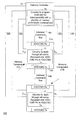
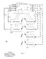
- FIG. 1 illustrates a point-to-point memory architecture having memory components daisy-chained to a low latency address bus according to an embodiment.
- FIG. 2 illustrates memory depth expansion using the point-to-point memory architecture of FIG. 1 .
- FIG. 3 illustrates a process for using the initial memory component of FIG. 1 .
- FIG. 4 illustrates memory width expansion using the point-to-point memory architecture of FIG. 1 .
- FIG. 5 illustrates a system with memory components daisy chained from the transmit interface of a memory controller.
- FIG. 6 is a timing diagram for memory components 51 A and 51 B of the system shown in FIG. 5 .
- FIG. 7 illustrates a system utilizing principles described with respect to FIG. 4 for memory width expansion in combination with the principles described with respect to FIG. 5 for memory depth expansion.
- FIG. 1 illustrates a point-to-point memory architecture having memory components daisy-chained to a low latency address bus according to an embodiment.
- the system 100 includes a memory controller 20 having point-to-point connections to a plurality of memory components 21 A and 21 B, which can be any type of discrete integrated circuits used for storage.
- the memory components 21 A and 21 B are daisy chained to the memory controller 20 , meaning that only the first memory component 21 A may be directly connected to a command interface of the memory controller 20 .
- the data bus 13 A-B and 15 A-B each of the memory components 21 A and 21 B are directly connected, meaning that all of the memory components 21 A and 21 B may be directly connected to a data interface of the memory controller 20 .
- the first memory component 21 A includes a circuitry 11 configured to immediately ripple through all commands received over the address bus 14 A.
- the circuitry 11 can be an internal connection between the address/command receiver 17 A and the address command transmitter 19 A. Since these commands can be immediately rippled through, e.g. there is no queuing and/or buffering needed, the memory component 21 B can receive re-transmitted commands over bus 14 B with minimal added latency. It should be apparent that the circuitry 11 is not burdened with complex analysis to determine which commands are to be rippled through.
- the width of the data interfaces on the memory components 21 A and 21 B is a fraction of a width of the data interface of the memory controller.
- the point-to-point data buses 13 A and 15 A can connect to an initial portion of a data interface on the memory controller 20
- the remaining memory component 21 B connects to the remaining portion of the data interface via the data buses 13 B and 15 B.
- the memory components 21 A and 21 B may have a fraction of the pin count of the memory controller 20 .
- the width of the data buses extending to and from each memory component 21 A and 21 B may be a fraction of the width of the computing system.
- the system 100 provides flexibility in that the width of the memory component 21 A and 21 B may be different than the width of the memory controller 20 .
- This quality allows the memory controller 20 to be configured with software or circuitry 10 that allows the controller 20 to be programmed for interoperability with a plurality of memory width/depth combinations.
- FIG. 2 An example will be shown in FIG. 2 to illustrate how the circuitry 10 can be used to expand the depth of a memory system.
- FIG. 4 to illustrate how the circuitry 10 can be used to expand the width of a memory system.
- the buses 13 A, 13 B, 15 A, and 15 B are serial buses. However, it should be apparent that it is both possible and practical to apply the principles described above to systems containing parallel data buses.
- memory components 21 A and 21 B can be architecturally identical. It should be apparent that this provides ease of configuration and ease of manufacture.
- the system 100 is particularly suited to the networking environment where relatively large word widths, e.g. one hundred and forty four bits, are used. In such an environment, the reduced number of links routed to each memory component is particularly helpful. It should be apparent that, by comparison to some conventional systems the present system 100 uses 1/Nth the number of links routed to each memory component, where N is equal to the number of memory components used. Although the principles described herein are applicable in the networking environment and other environments using relatively high bit width, it is both possible and practical to apply the principles described herein to any memory systems, such as thirty two bit memory systems.
- SRAM Static Random Access Memory
- FIG. 2 illustrates memory depth expansion using the point-to-point memory architecture of FIG. 1 .
- the example system 200 expands memory depth by operating two forty bit memory components 30 A and 30 B with an eighty bit memory controller 40 .
- memory depth refers to the number of bits available for each bit of width.
- the system 200 effectively doubles memory depth by accessing a word using two memory components instead of one.
- the following paragraphs provide an example of a write operation in the system 200 .
- the memory controller 40 sends the word out over the interface 23 .
- the first forty bits of the word are sent over the bus 13 A, which in the present example is a serial bus having five serial links.
- the second forty bits of the word are sent over a different portion of the same interface 23 and over the other bus 13 B.
- the two halves of the word are respectively received at interfaces 33 A and 33 B.
- the controller 40 also sends a single write communication over the address bus 14 A.
- the single write communication provides the memory space addresses to write the word. Since the address space extends over two memory components, the addresses contained in the write communication correspond to locations in both memories.
- the memory component 30 A receives the write communication over the receiver 17 A.
- the memory component 30 A acts on the write communication as it corresponds to a location on the component 30 A thereby writing the first half of the word to that local location.
- the circuitry 11 also ripples the write communication through to the transmitter 19 A for re-transmission over the bus 14 B. Instead of spending latency determining which portion of the write communication corresponds to the component 30 B, the circuitry 30 A re-transmits the entire write communication via the transmitter 19 A.
- the operation is similar to a loop back technique used to self test a wireless transceiver's transmitter and receiver.
- the component 30 B writes the remaining half of the word (received over input interface 33 B) according to the write communication from the bus 14 B.
- the memory component 30 B may contain the circuitry 11 as well, although in the present example with two components there is no bus connected to the transmitter 19 B.
- a read command operates in a similar fashion. After receiving the read communication over the buses 14 A and 14 B, the memory components 30 A and 30 B output the requested word over the interfaces 33 A and 33 B.
- the transmission latency associated with the data buses 13 A-B and the address buses 15 A-B can be different, in particular, because of latency added by rippling through the commands.
- a compensation technique can be used to avoid misalignment of the command and the data.
- the memory component 30 A can be configured to impose a delay on the data received over the bus 13 A to align this data with the command received over the receiver 17 A.
- the memory component 30 B can impose a longer delay on the data received over the bus 13 B to align this data with the command received over the address bus 14 B as this command will be received later in time than the command received by the memory component 30 A.
- This delay can be implemented using registers, First In First Out (FIFO) buffers, or any other known mechanism for imposing a delay.
- the delay can be programmable on each memory component depending on that memory components position along the daisy chain.
- Another type of imposed delay that can be used is a delay by the memory controller 40 to ensure that data received over the buses 15 A-B can be associated with the command sent over the address bus 14 A.
- the delay applied by the memory controller 40 corresponds to the delay applied by the memory components as the memory component's delay affects the difference in time between the memory controller 40 transmitting the command and receiving back the data.
- the depth expansion can be performed even when the memory components have the same width as the memory controller.
- the memory components 30 A and 30 B were manufactured as eighty bit components, half of the interfaces 33 A and 33 B could be powered down.
- the circuitry 10 allows the memory controller 40 to be programmed for the above described depth expansion. Accordingly, the controller 40 can interface with, for example, an eighty bit wide memory component, two forty bit wide memory components, four twenty bit wide memory components, etc. It should be understood that the circuitry 10 can also be used to program the memory components to use a reduced number of inputs and outputs, thus increasing the memory depth by the same ratio, e.g. the depth at forty bits will be 2 ⁇ the depth at eight bits and the depth at twenty bits will be 4 ⁇ the depth at eighty bits. Depending on the configuration, the system 200 will have different memory depth.
- system 200 can be implemented by updating existing memory controllers with software configured for the above described functionality.
- the software may account for a latency difference. Otherwise existing controllers do not specify any hardware change to receive words from two or more components.
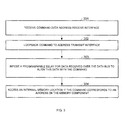
- FIG. 3 illustrates a process for using the initial memory component of FIG. 1 .
- the memory component receives a command over the address receive interface.
- the memory component loops back the command to an address transmit interface.
- the memory component can impose a programmable delay to data received over the data interface. This programmable delay is to align the received data with the command received over the address receive interface. The duration of this delay is dependent on the memory component's position along the daisy chain.
- the memory component accesses a memory location according to the command if the command corresponds to a local address location.
- block 303 may not be needed.
- some systems tolerate misalignment of up to ten times the cycle time, e.g. ten nanoseconds in a system with a ten Gigahertz operating frequency.
- the programmed amount can be set according to empirical analysis of measured latency for each memory component propagating received commands. Accordingly, counting outwards from the initial memory component, each memory component is programmed to impose a progressively larger programmable delay with the last memory component in the series programmed to impose the largest delay.
- the programmable delay can also be computed by each memory component according to inputs. For example, based on an input indicating the amount of memory components connected in series along the address bus as well as an indication of the memory component's position in the series, the memory component can determine a time delay to be imposed.
- FIG. 4 illustrates memory width expansion using the point-to-point memory architecture of FIG. 1 .
- the example system 300 is used to illustrate width expansion, or width adjustment, using the circuitry 10 on the memory controller 50 .
- the memory controller 50 is a one hundred and sixty bit memory controller that can operate in a plurality of bit width modes, including a first eighty bit mode as indicated by the solid lines and a second one hundred and sixty bit mode as indicated by the dashed lines.
- the system 300 operates as an eighty bit wide system. Since the controller 43 is operating with forty bit memories 41 A-B, certain buses ( 45 C-D) and interface portions of the interface 43 can be disabled for power savings as indicated by the “x” markings. It should be apparent that some of the data bus connections and part of the memory controller 50 in the first mode have been shown for ease of illustration.
- the system 300 can operate with as a one hundred and sixty bit wide system using similar hardware. Specifically, the width may be adjusted to one hundred and sixty bits by using two additional memories ( 41 C-D), and by powering the memory controller's entire data interface 43 and all the data buses 45 A-D. It should be apparent that some of the data bus connections and part of the memory controller 50 in the second mode have been shown for ease of illustration.
- the circuitry 10 provides the capability for width adjustment. Either mode can be selected using the circuitry 10 thus allowing the same hardware to be used for different bit wide systems depending on user preference and application needs. It should be understood that there is no limitation to the amount of modes that can be provided by the circuitry 10 , for example, the circuitry 10 can configure the system 300 for a third mode of forty bits with the memory component 41 A utilized.
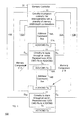
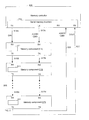
- FIG. 5 illustrates a system with memory components daisy chained from the transmit interface of a memory controller.
- the system 500 includes a memory controller 505 having a connection 515 A/ 517 A from the transmit portion of the serial memory interface 512 to a memory component 51 A, which can be any type of discrete integrated circuit used for storage.
- a memory component 51 A which can be any type of discrete integrated circuit used for storage.
- the memory components 51 A- 51 N are daisy chained to the memory controller 505 , meaning that only the first memory component 51 A may be directly connected to a transmit portion of the interface 512 of the memory controller 505 .
- this portion has a point-to-point connection directly to a transmit interface of the last memory component 51 N in the daisy chain.
- the memory component 51 A has the transmit portion of its data interface connected to the receive portion of the data interface of the memory component 51 B.
- the memory component 51 B has the transmit portion of its data interface connected to the receive portion of the data interface of a next memory component.
- the last memory component 51 N has the receive portion of its data interface to a previous memory component.
- the transmit portion of the last memory component 51 N is connected to the receive portion of the interface 512 of the memory controller 505 .
- the width of the data interfaces on the memory components 51 A-N matches a width of the data portion of the interface 512 of the memory controller.
- the memory components 51 A-N include circuitry 511 configured to immediately ripple through commands received over the address bus 517 A.
- the circuitry 511 can be an internal connection between the address/command receiver of the memory component and the address command transmitter of the memory component. Since these commands can be immediately rippled through, e.g. there is no queuing and/or buffering needed, the memory component 51 B can receive re-transmitted commands over bus 517 B with minimal added latency.
- Each memory component 51 A-N has a configuration specified by, for example, a bonding option, bit setting, or other mechanism for configuring the memory components 51 A-N.
- This configuration mechanism is used to allocate a respective portion of a memory space to each memory component 51 A-N.
- the memory component 51 A is configured with an initial portion of a memory space
- the memory component 51 B is configured with a next portion of the memory space
- the memory component 51 N is configured with a last portion of the memory space.
- the memory space thus extends over more than one memory component.
- the first memory component 51 A compares an address of a command received over connection 517 A to an assigned address range. If there is a match, the first memory component 51 A performs an internal access according to the received command and sends out a NOP instruction over connection 517 B. The NOP instruction blocks other memory components 51 B-N further down the chain from operating in response to the command. If there is no match, the circuitry 511 passes the received command over the connection 517 B to the next memory component 51 B. This process continues through the daisy chain (a NOP is finally sent over connection 525 ).
- the memory component 51 A looks up the data and sends it out over connection 515 B to be passed through the other memory components 51 B-N via connections 515 B-N and 527 .
- the received command is a write on an address in a memory range of the memory component 51 A
- the memory component 51 A receives data to be written over connection 515 A.
- An acknowledgement for the write is finally sent over connections 515 B-N and 527 .
- the system 500 provides flexibility with memory depth.
- the memory controller 505 has a same interface 512 regardless of the number of memory components 51 A-N that are daisy chained to the transmit portion of the interface 512 of the memory controller 505 .
- the memory width e.g. width of the interface 512
- the memory width can be maintained as depth is expanded/reduced by varying the number of memory components.
- memory components 51 A-N can be architecturally identical to each other. It should be apparent that this provides ease of configuration and ease of manufacture. It should be apparent that the configuration discussed earlier can be performed after a manufacture process.
- the above described configuration of the system 500 has bus routing advantages when compared to other systems. As the number of memory components in the system 500 is increased, there is very little corresponding trace added. For example, it should be apparent that each additional memory component requires only one additional data bus, rather than two additional data buses in other designs (due to the single memory controller receive data bus 527 ).
- each of the memories 41 A- 41 D ( FIG. 4 ) includes at least one other memory component attached thereto.
- Each of the memories 41 A- 41 D ripples through commands to the attached memory component(s) over a data bus.
- the transmit interface of the attached memory component is attached to the receive interface of the memory controller 50 .
- the resulting system has both width and depth expansion. This will be discussed later in more detail with respect to FIG. 7 , after continuing the discussion of the present system 500 with respect to FIG. 6 .
- FIG. 6 is a timing diagram for memory components 51 A and 51 B of the system shown in FIG. 5 .
- the memory component 51 A receives over an address bus to the memory controller a write W 1 to its assigned address range.
- the memory component 51 A also receives data Din 1 and crcW 1 over respective channels of a data bus to the memory controller.
- the crcW 1 is associated with address W 1 and data Din 1 .
- the memory component 51 A transmits NOP over the address bus, since the write W 1 is within its address range.
- the memory component 51 A also outputs a NOP over the data bus since there is no data output on a write.
- An acknowledgement can also be output for a CRC check.
- the NOPs and the acknowledgement are received at the memory component 51 B (accounting for channel latency associated with transmission over the bus).
- the memory component 51 B passes the NOPs and the acknowledgement to a next memory component at time t 11 .
- the timing diagram of FIG. 6 also shows the processing with a read to the memory component 51 A, a write to the memory component 51 B, and a read to the memory component 51 B.
- a read to the memory component 51 A Referring to the write to memory component 51 B (W 2 ), at time t 3 the memory component 51 A receives the W 2 command and the data to be written. After the comparison indicates no match to the address range of the memory component 51 A, at time t 7 the memory component 51 A passes the W 2 command and the data to be written back out over the bus to be received and processed by the next memory component 51 B as shown.
- timing characteristics for the system 500 are apparent from the timing diagram of FIG. 1 .
- the system 500 maintains the same latency on the data bus as the address bus (data transmissions and address transmissions are aligned).
- the data channel of the data bus has 50% utilization, assuming equal numbers of reads and writes.
- the data channel on the receive interface of the memory device 51 A has two of four time slots empty (50% utilization) with two reads and two writes.
- the system 500 uses cycle-by-cycle CRC scheme with a CRC channel in the data bus.
- the transmit interface of the memory component 51 A sends transmissions over the CRC channel of the data bus at every one of times t 5 -t 8 . This is in contrast to some other memory systems having a data-by-data CRC check (CRCs are accumulated/delayed to align CRC transmission with data transfers or other reasons).
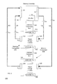
- FIG. 7 illustrates a system utilizing principles described with respect to FIG. 4 for memory width expansion in combination with the principles described with respect to FIG. 5 for memory depth expansion.
- the memory controller 705 has width expansion, namely a 20 bit transmit interface is coupled to 10 bit memories A 1 and A 2 .
- the memories A 1 and A 2 each have at least one memory N 1 and N 2 respectively coupled as shown thereto for depth expansion.
- Memory A 1 ripples through received commands to memory A 2 as shown, similar to FIG. 4 .
- Latency is configured in the system 700 so that the latency associated with passing a command from memory A 1 to memory A 2 corresponds to the latency for memory A 1 to process and transmit data out of the TX interface of memory A 1 .
- This allows memory N 1 to receive aligned address and data transmissions.
- Address control is performed similar to FIGS. 4 and 5 , namely by configuring the memory controller 705 and setting the address ranges of the memory components A 1 , A 2 , N 1 , and N 2 .
- the system described above can use dedicated processor systems, micro controllers, programmable logic devices, or microprocessors that perform some or all of the operations. Some of the operations described above may be implemented in software and other operations may be implemented in hardware.
Abstract
Description
Claims (20)
Priority Applications (3)
| Application Number | Priority Date | Filing Date | Title |
|---|---|---|---|
| US12/819,794 US8856434B2 (en) | 2008-09-26 | 2010-06-21 | Memory system and method |
| CN201110167651.6A CN102289417B (en) | 2010-06-21 | 2011-06-21 | Memory system and method |
| TW100121577A TWI564724B (en) | 2010-06-21 | 2011-06-21 | Memory system and method |
Applications Claiming Priority (2)
| Application Number | Priority Date | Filing Date | Title |
|---|---|---|---|
| US12/239,532 US8095747B2 (en) | 2008-09-26 | 2008-09-26 | Memory system and method |
| US12/819,794 US8856434B2 (en) | 2008-09-26 | 2010-06-21 | Memory system and method |
Related Parent Applications (1)
| Application Number | Title | Priority Date | Filing Date |
|---|---|---|---|
| US12/239,532 Continuation-In-Part US8095747B2 (en) | 2008-09-26 | 2008-09-26 | Memory system and method |
Publications (2)
| Publication Number | Publication Date |
|---|---|
| US20110252162A1 US20110252162A1 (en) | 2011-10-13 |
| US8856434B2 true US8856434B2 (en) | 2014-10-07 |
Family
ID=44761736
Family Applications (1)
| Application Number | Title | Priority Date | Filing Date |
|---|---|---|---|
| US12/819,794 Active 2030-08-14 US8856434B2 (en) | 2008-09-26 | 2010-06-21 | Memory system and method |
Country Status (1)
| Country | Link |
|---|---|
| US (1) | US8856434B2 (en) |
Families Citing this family (6)
| Publication number | Priority date | Publication date | Assignee | Title |
|---|---|---|---|---|
| US8825967B2 (en) * | 2011-12-08 | 2014-09-02 | Conversant Intellectual Property Management Inc. | Independent write and read control in serially-connected devices |
| CN103532769A (en) * | 2012-07-06 | 2014-01-22 | 成都林海电子有限责任公司 | Information interaction test method for satellite mobile communication terminal based on Beidou |
| CN103902472B (en) * | 2012-12-28 | 2018-04-20 | 华为技术有限公司 | Internal storage access processing method, memory chip and system based on memory chip interconnection |
| US10140222B1 (en) | 2017-07-06 | 2018-11-27 | Micron Technology, Inc. | Interface components |
| WO2020254732A1 (en) * | 2019-06-21 | 2020-12-24 | Luos Robotics | Decentralised communication system and corresponding control method |
| US11494324B2 (en) | 2019-08-29 | 2022-11-08 | Microchip Technology Incorporated | Daisy chain streaming mode |
Citations (10)
| Publication number | Priority date | Publication date | Assignee | Title |
|---|---|---|---|---|
| US6625687B1 (en) * | 2000-09-18 | 2003-09-23 | Intel Corporation | Memory module employing a junction circuit for point-to-point connection isolation, voltage translation, data synchronization, and multiplexing/demultiplexing |
| US20040054845A1 (en) * | 2001-04-24 | 2004-03-18 | Rambus, Inc. | Method and apparatus for signaling between devices of a memory system |
| US20050099384A1 (en) * | 2003-10-22 | 2005-05-12 | Benq Corporation | Panel display |
| US7013359B1 (en) | 2001-12-21 | 2006-03-14 | Cypress Semiconductor Corporation | High speed memory interface system and method |
| CN1926632A (en) | 2004-03-02 | 2007-03-07 | 英特尔公司 | Interchangeable connection arrays for double-sided memory module placement |
| US20070070669A1 (en) | 2005-09-26 | 2007-03-29 | Rambus Inc. | Memory module including a plurality of integrated circuit memory devices and a plurality of buffer devices in a matrix topology |
| US20080028126A1 (en) * | 2006-07-26 | 2008-01-31 | Gerald Keith Bartley | Memory System Having an Apportionable Data Bus and Daisy Chained Memory Chips |
| US20080028176A1 (en) | 2006-07-26 | 2008-01-31 | Gerald Keith Bartley | Memory system having self timed daisy chained memory chips |
| US20090164677A1 (en) | 2007-12-21 | 2009-06-25 | Rambus, Inc. | Timing adjustment in a reconfigurable system |
| US8095747B2 (en) * | 2008-09-26 | 2012-01-10 | Cypress Semiconductor Corporation | Memory system and method |
-
2010
- 2010-06-21 US US12/819,794 patent/US8856434B2/en active Active
Patent Citations (11)
| Publication number | Priority date | Publication date | Assignee | Title |
|---|---|---|---|---|
| US6625687B1 (en) * | 2000-09-18 | 2003-09-23 | Intel Corporation | Memory module employing a junction circuit for point-to-point connection isolation, voltage translation, data synchronization, and multiplexing/demultiplexing |
| US20040054845A1 (en) * | 2001-04-24 | 2004-03-18 | Rambus, Inc. | Method and apparatus for signaling between devices of a memory system |
| US20070255919A1 (en) | 2001-04-24 | 2007-11-01 | Ware Frederick A | Memory controller device having timing offset capability |
| US7013359B1 (en) | 2001-12-21 | 2006-03-14 | Cypress Semiconductor Corporation | High speed memory interface system and method |
| US20050099384A1 (en) * | 2003-10-22 | 2005-05-12 | Benq Corporation | Panel display |
| CN1926632A (en) | 2004-03-02 | 2007-03-07 | 英特尔公司 | Interchangeable connection arrays for double-sided memory module placement |
| US20070070669A1 (en) | 2005-09-26 | 2007-03-29 | Rambus Inc. | Memory module including a plurality of integrated circuit memory devices and a plurality of buffer devices in a matrix topology |
| US20080028126A1 (en) * | 2006-07-26 | 2008-01-31 | Gerald Keith Bartley | Memory System Having an Apportionable Data Bus and Daisy Chained Memory Chips |
| US20080028176A1 (en) | 2006-07-26 | 2008-01-31 | Gerald Keith Bartley | Memory system having self timed daisy chained memory chips |
| US20090164677A1 (en) | 2007-12-21 | 2009-06-25 | Rambus, Inc. | Timing adjustment in a reconfigurable system |
| US8095747B2 (en) * | 2008-09-26 | 2012-01-10 | Cypress Semiconductor Corporation | Memory system and method |
Non-Patent Citations (8)
| Title |
|---|
| International Search Report for International Application No. PCT/US08/86695 dated Feb. 6, 2009; 2 pages. |
| Rami Marwan Nasr, "FBSIM and the Fully Buffered DIMM Memory System Architecture," University of Maryland, 2005, 138 pages. |
| SIPO 1st Office Action for Application No. 20091017898.8 dated Jun. 6, 2013; 5 pages. |
| SIPO Office Action for Application No. 20091017898.8 dated Feb. 17, 2013; 5 pages. |
| TIPO Office Action for Application No. 97149679.0 dated Jan. 22, 2014; 4 pages. |
| USPTO Non Final Rejection for U.S. Appl. No. 12/239,532 dated Jul. 5, 2011; 8 pages. |
| USPTO Notice of Allowance for U.S. Appl. No. 12/239,532 dated Oct. 19, 2011; 5 pages. |
| Written Opinion of the International Searching Authority for International Application No. PCT/US08/86695 dated Feb. 6, 2009; 7 pages. |
Also Published As
| Publication number | Publication date |
|---|---|
| US20110252162A1 (en) | 2011-10-13 |
Similar Documents
| Publication | Publication Date | Title |
|---|---|---|
| US8856434B2 (en) | Memory system and method | |
| JP5571288B2 (en) | Hub device, method for selecting prefetch mode, memory system, and memory subsystem | |
| US8296541B2 (en) | Memory subsystem with positional read data latency | |
| CN101405708B (en) | Memory systems for automated computing machinery | |
| US10224080B2 (en) | Semiconductor memory device with late write feature | |
| US7606988B2 (en) | Systems and methods for providing a dynamic memory bank page policy | |
| US7342816B2 (en) | Daisy chainable memory chip | |
| US7545664B2 (en) | Memory system having self timed daisy chained memory chips | |
| CN101583934A (en) | Memory system including a high-speed serial buffer | |
| US8095747B2 (en) | Memory system and method | |
| US7345900B2 (en) | Daisy chained memory system | |
| US7546410B2 (en) | Self timed memory chip having an apportionable data bus | |
| US7673093B2 (en) | Computer system having daisy chained memory chips | |
| US7345901B2 (en) | Computer system having daisy chained self timed memory chips | |
| US7620763B2 (en) | Memory chip having an apportionable data bus | |
| US11442878B2 (en) | Memory sequencer system and a method of memory sequencing using thereof | |
| US7627711B2 (en) | Memory controller for daisy chained memory chips | |
| US20120117286A1 (en) | Interface Devices And Systems Including The Same | |
| US7490186B2 (en) | Memory system having an apportionable data bus and daisy chained memory chips | |
| US20080028125A1 (en) | Computer System Having an Apportionable Data Bus | |
| US7577811B2 (en) | Memory controller for daisy chained self timed memory chips | |
| TWI564724B (en) | Memory system and method | |
| US20080028160A1 (en) | Carrier having daisy chain of self timed memory chips | |
| US20080028161A1 (en) | Daisy chainable self timed memory chip | |
| US7617350B2 (en) | Carrier having daisy chained memory chips |
Legal Events
| Date | Code | Title | Description |
|---|---|---|---|
| AS | Assignment |
Owner name: CYPRESS SEMICONDUCTOR CORPORATION, CALIFORNIA Free format text: ASSIGNMENT OF ASSIGNORS INTEREST;ASSIGNORS:LI, JUN;LI, GABRIEL;REEL/FRAME:024568/0418 Effective date: 20100618 |
|
| STCF | Information on status: patent grant |
Free format text: PATENTED CASE |
|
| AS | Assignment |
Owner name: MORGAN STANLEY SENIOR FUNDING, INC., NEW YORK Free format text: SECURITY INTEREST;ASSIGNORS:CYPRESS SEMICONDUCTOR CORPORATION;SPANSION LLC;REEL/FRAME:035240/0429 Effective date: 20150312 |
|
| FEPP | Fee payment procedure |
Free format text: PAYOR NUMBER ASSIGNED (ORIGINAL EVENT CODE: ASPN); ENTITY STATUS OF PATENT OWNER: LARGE ENTITY |
|
| AS | Assignment |
Owner name: MONTEREY RESEARCH, LLC, CALIFORNIA Free format text: ASSIGNMENT OF ASSIGNORS INTEREST;ASSIGNOR:CYPRESS SEMICONDUCTOR CORPORATION;REEL/FRAME:040908/0960 Effective date: 20160928 |
|
| AS | Assignment |
Owner name: SPANSION LLC, CALIFORNIA Free format text: RELEASE BY SECURED PARTY;ASSIGNOR:MORGAN STANLEY SENIOR FUNDING, INC.;REEL/FRAME:041175/0939 Effective date: 20160928 Owner name: CYPRESS SEMICONDUCTOR CORPORATION, CALIFORNIA Free format text: RELEASE BY SECURED PARTY;ASSIGNOR:MORGAN STANLEY SENIOR FUNDING, INC.;REEL/FRAME:041175/0939 Effective date: 20160928 |
|
| MAFP | Maintenance fee payment |
Free format text: PAYMENT OF MAINTENANCE FEE, 4TH YEAR, LARGE ENTITY (ORIGINAL EVENT CODE: M1551) Year of fee payment: 4 |
|
| AS | Assignment |
Owner name: MORGAN STANLEY SENIOR FUNDING, INC., NEW YORK Free format text: CORRECTIVE ASSIGNMENT TO CORRECT THE 8647899 PREVIOUSLY RECORDED ON REEL 035240 FRAME 0429. ASSIGNOR(S) HEREBY CONFIRMS THE SECURITY INTERST;ASSIGNORS:CYPRESS SEMICONDUCTOR CORPORATION;SPANSION LLC;REEL/FRAME:058002/0470 Effective date: 20150312 |
|
| MAFP | Maintenance fee payment |
Free format text: PAYMENT OF MAINTENANCE FEE, 8TH YEAR, LARGE ENTITY (ORIGINAL EVENT CODE: M1552); ENTITY STATUS OF PATENT OWNER: LARGE ENTITY Year of fee payment: 8 |