US8855244B2 - Digitally demodulating a minimum-shift keying (MSK) signal - Google Patents
Digitally demodulating a minimum-shift keying (MSK) signal Download PDFInfo
- Publication number
- US8855244B2 US8855244B2 US13/331,016 US201113331016A US8855244B2 US 8855244 B2 US8855244 B2 US 8855244B2 US 201113331016 A US201113331016 A US 201113331016A US 8855244 B2 US8855244 B2 US 8855244B2
- Authority
- US
- United States
- Prior art keywords
- msk
- symbols
- symbol
- consecutive
- signal
- Prior art date
- Legal status (The legal status is an assumption and is not a legal conclusion. Google has not performed a legal analysis and makes no representation as to the accuracy of the status listed.)
- Active, expires
Links
Images


Classifications
-
- H—ELECTRICITY
- H04—ELECTRIC COMMUNICATION TECHNIQUE
- H04L—TRANSMISSION OF DIGITAL INFORMATION, e.g. TELEGRAPHIC COMMUNICATION
- H04L27/00—Modulated-carrier systems
- H04L27/18—Phase-modulated carrier systems, i.e. using phase-shift keying
- H04L27/20—Modulator circuits; Transmitter circuits
- H04L27/2032—Modulator circuits; Transmitter circuits for discrete phase modulation, e.g. in which the phase of the carrier is modulated in a nominally instantaneous manner
- H04L27/2053—Modulator circuits; Transmitter circuits for discrete phase modulation, e.g. in which the phase of the carrier is modulated in a nominally instantaneous manner using more than one carrier, e.g. carriers with different phases
- H04L27/206—Modulator circuits; Transmitter circuits for discrete phase modulation, e.g. in which the phase of the carrier is modulated in a nominally instantaneous manner using more than one carrier, e.g. carriers with different phases using a pair of orthogonal carriers, e.g. quadrature carriers
- H04L27/2067—Modulator circuits; Transmitter circuits for discrete phase modulation, e.g. in which the phase of the carrier is modulated in a nominally instantaneous manner using more than one carrier, e.g. carriers with different phases using a pair of orthogonal carriers, e.g. quadrature carriers with more than two phase states
- H04L27/2078—Modulator circuits; Transmitter circuits for discrete phase modulation, e.g. in which the phase of the carrier is modulated in a nominally instantaneous manner using more than one carrier, e.g. carriers with different phases using a pair of orthogonal carriers, e.g. quadrature carriers with more than two phase states in which the phase change per symbol period is constrained
- H04L27/2082—Modulator circuits; Transmitter circuits for discrete phase modulation, e.g. in which the phase of the carrier is modulated in a nominally instantaneous manner using more than one carrier, e.g. carriers with different phases using a pair of orthogonal carriers, e.g. quadrature carriers with more than two phase states in which the phase change per symbol period is constrained for offset or staggered quadrature phase shift keying
-
- H—ELECTRICITY
- H04—ELECTRIC COMMUNICATION TECHNIQUE
- H04L—TRANSMISSION OF DIGITAL INFORMATION, e.g. TELEGRAPHIC COMMUNICATION
- H04L27/00—Modulated-carrier systems
- H04L27/10—Frequency-modulated carrier systems, i.e. using frequency-shift keying
- H04L27/14—Demodulator circuits; Receiver circuits
-
- H—ELECTRICITY
- H04—ELECTRIC COMMUNICATION TECHNIQUE
- H04L—TRANSMISSION OF DIGITAL INFORMATION, e.g. TELEGRAPHIC COMMUNICATION
- H04L25/00—Baseband systems
- H04L25/02—Details ; arrangements for supplying electrical power along data transmission lines
- H04L25/06—DC level restoring means; Bias distortion correction ; Decision circuits providing symbol by symbol detection
- H04L25/067—DC level restoring means; Bias distortion correction ; Decision circuits providing symbol by symbol detection providing soft decisions, i.e. decisions together with an estimate of reliability
-
- H—ELECTRICITY
- H04—ELECTRIC COMMUNICATION TECHNIQUE
- H04L—TRANSMISSION OF DIGITAL INFORMATION, e.g. TELEGRAPHIC COMMUNICATION
- H04L27/00—Modulated-carrier systems
- H04L27/18—Phase-modulated carrier systems, i.e. using phase-shift keying
- H04L27/20—Modulator circuits; Transmitter circuits
Definitions
- the present disclosure relates to digital communications, and more particularly, to an advanced signal processing data path that allows recovering transmitting data bits from a minimum shift keying (MSK) modulated waveform signal, with high robustness against impairments of the analog radio and the propagation medium.
- MSK minimum shift keying
- MSK Minimum Shift Keying
- MSK is a type of continuous-phase frequency-shift keying that was developed in the late 1950s and 1960s, see U.S. Pat. No. 2,977,417, entitled “Minimum-Shift Data Communication System,” by Doelz et al., and incorporated by reference herein for all purposes.
- MSK is encoded with bits alternating between quadrature components, with the Q component delayed by half the symbol period.
- MSK encodes each bit as a half sinusoid. This results in a constant-modulus signal which reduces problems caused by non-linear distortion.
- MSK can also be viewed as a continuous phase frequency shift keyed (CPFSK) signal with a frequency separation of one-half the bit rate.
- CPFSK continuous phase frequency shift keyed
- a static frequency shift of +1 Hz means that the phase is constantly advancing at the rate of 360 degrees per second (2 ⁇ radians/second) relative to the phase of the unshifted signal.
- a static frequency shift of ⁇ 1 Hz means that the phase is constantly retarding at the rate of ⁇ 360 degrees per second ( ⁇ 2 ⁇ radians/second) relative to the phase of the unshifted signal.
- phase shifts can be detected by sampling phase at each symbol period.
- Phase shifts of (2N+1) ⁇ /2 radians are easily detected with an I/Q demodulator.
- the polarity of the I channel conveys the transmitted data
- the polarity of the Q channel conveys the data.
- the minimum frequency shift which yields orthogonality of I and Q is that which results in a phase shift of ⁇ /2 radians per symbol (90 degrees per symbol). The deviation must be accurate in order to generate repeatable 90 degree phase shifts.
- a phase shift of +90 degrees represents a data bit equal to “1”, while ⁇ 90 degrees represents a “0”.
- the peak-to-peak frequency shift of an MSK signal is equal to one-half of the bit rate.
- the MSK signal produces a constant envelope carrier (no carrier amplitude variations) which is not affected by amplification through a higher efficiency non-linear amplifier, e.g., class C amplifier.
- a higher efficiency non-linear amplifier e.g., class C amplifier.
- It is a spectrally efficient modulation scheme (see GMSK below), has good bit error rate (BER) performance and is self synchronizing. These are all desirable characteristics for improving the power efficiency of receivers and transmitters, especially those operated from a battery.
- Amplitude variations can exercise nonlinearities in an amplifier's amplitude-transfer function, generating spectral regrowth, a component of adjacent channel power. Therefore, more efficient amplifiers (which tend to be less linear) can be used with constant-envelope signals, thereby reducing power consumption.
- MSK has a narrower spectrum than wider deviation forms of frequency shift keying (FSK).
- the width of the spectrum is also influenced by the waveforms causing the frequency shift. If those waveforms have fast transitions or a high slew rate, then the spectrum of the transmitter will be broad.
- the waveforms are filtered with a Gaussian filter, resulting in a narrow spectrum.
- the Gaussian filter has no time-domain overshoot that would broaden the spectrum by increasing the peak deviation.
- MSK in combination with a Gaussian filter is termed GMSK (Gaussian MSK).
- IEEE standard 802.15.4-2006 Part 15.4: Wireless Medium Access Control (MAC) and Physical Layer (PHY) Specifications for Low-Rate Wireless Personal Area Networks (WPANs), incorporated by reference herein for all purposes, defines the protocol and compatible interconnection for data communication devices using low-data-rate, low-power, and low-complexity short-range radio frequency (RF) transmissions in a wireless personal area network (WPAN) at data transfer rates of up to a 250 kilobit/second (kb/s). However with increased demand for content rich wireless data transfer, 250 kb/s is not fast enough. Up to a two (2) megabit per second (Mb/s) wireless data rate is desired as a selectable option for increased data transfer in a IEEE standard 802.15.4 compatible wireless device. With the constraints of a given analog radio, achieving this requirement would not be possible without advanced digital signal processing techniques.
- RF radio frequency
- the method processes a sampled stream of I-Q format MSK modulated symbols; receives the input through a three symbol wide sliding window; for each window position rates all the eight possible combinations of three modulating symbols as to the likelihood of being the source for the current, possibly impaired input waveform segment; computes the ratings from the I-Q waveform of the input as the linearly quantized outputs of a bank of matched filters; based on the fact that the ratings are related through the common symbols in the overlap of consecutive window positions, constructs a 4 state trellis and assigns the branch metrics from the ratings to represent the probabilistic relation between the sequence of ratings; and uses the trellis to drive a Viterbi decoder to recover (find the best estimate for) the data represented by the sequence of sampled I-Q format MSK symbols.
- a method for digitally demodulating a minimum-shift keying (MSK) signal may method comprise the steps of: receiving a sequence of sampled I-Q format MSK symbols; processing three symbols at a time of the received sequence of sampled I-Q format MSK symbols, selected by using a sliding window; rating all eight possible combinations of three modulating symbols as to the likelihood of being a source for a currently processed and possibly impaired input waveform segment; computing the ratings from the I-Q waveform of the three input symbols by a bank of matched filters; defining a trellis that represents a probabilistic relationship within a sequence of ratings based on ratings that are related through common symbols in an overlap of consecutive window positions; and using the trellis to drive a Viterbi decoder to find a best estimate for each of the individual modulating symbols.
- MSK minimum-shift keying
- the step of selecting the three consecutive MSK symbols is done with a sliding three symbol window.
- the step of rating hypotheses for each combination of the three consecutive MSK symbols is done with the linearly quantized outputs of a bank of matched filters each filter covering one of the eight possible combination of three consecutive MSK symbols.
- the trellis is constructed from four (4) memory states corresponding to the four (4) possible combination of two (2) MSK symbols and the computed ratings are assigned as branch metrics to the transitions between the memory states such that they represent the probabilistic relationship between them as established by the three symbol sliding window.
- the constructed trellis is used in the Viterbi algorithm to find the best estimate for the data represented by the sequence of sampled I-Q format MSK symbols.
- the ADC is a one (1) bit ADC.
- the one (1) bit ADC output is fed through a decimating filter producing four (4) in-phase (I) bits and four (4) quadrature phase (Q) bits.
- an apparatus for digitally demodulating a minimum-shift keying (MSK) signal may comprise: an analog-to-digital converter (ADC) for sampling the MSK signal and converting the sampled MSK signal into a plurality of digital representations thereof; a down-conversion filter for decimating the digital representations of the sampled data signals and converting the decimated digital representations of the sampled data signals to in-phase (I) and quadrature phase (Q) MSK symbols; a three MSK symbol window for selecting three consecutive MSK symbols; a matched filter bank for rating hypotheses for each combination of the selected three consecutive MSK symbols; and a Viterbi decoder for selecting a highest rated hypothesis for the combination of the three consecutive MSK symbols and to provide a most likely logic level for each of the selected three consecutive MSK symbols.
- ADC analog-to-digital converter
- Q quadrature phase
- the MSK signal is frequency translated in a frequency mixer down to a zero intermediate frequency (IF) before the MSK signal is sampled.
- the ADC is a one (1) bit ADC.
- the down-conversion filter decimates the one (1) bit ADC output to four (4) in-phase (I) bits and four (4) quadrature phase (Q) bits.
- the three symbol window is a sliding three symbol window.
- the matched filter bank comprises eight linearly quantized filters configured to rate the hypotheses for each combination of the selected three consecutive MSK symbols.
- FIG. 1 illustrates a schematic block diagram of a wireless MSK receiver coupled to a digital processor, according to a specific example embodiment of this disclosure
- FIG. 2 illustrates schematic waveform diagrams of an ideal MSK I-Q signal and the samples thereof as input to the MSK receive chain in the wireless receiver shown on FIG. 1 ;
- FIG. 3 illustrates schematic waveform diagrams of a plurality of MSK symbols with a sliding window over three of the MSK symbols, according to the teachings of this disclosure
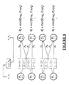
- FIG. 4 illustrates a schematic waveform and the block diagram of a matched filter bank matching the received samples against all possible combinations of three sequential MSK symbols, according to the teachings of this disclosure
- FIG. 5 illustrates a conceptual arrangement for the digital MSK receive chain
- FIG. 6 illustrates the experimental result that validates the use of the outputs of the matched filter bank as the log-likelihood-ratios in the Viterbi decision process
- FIG. 7 illustrates a sliding window comprising three of a plurality of sequential MSK symbols and the building block of a trellis diagram thereof, according to the teachings of this disclosure
- FIG. 8 illustrates graphical details of a slice of the trellis diagram for the Viterbi decision process used in determining the received MSK symbols, according to the teachings of this disclosure.
- FIG. 9 illustrates a graphical plot of performance characteristics, according to the teachings of this disclosure.
- This disclosure presents a method and apparatus for demodulating and decoding an MSK signal stream from its sampled and digitized I-Q representation contaminated by noise during transmission and distorted by impairments accumulated while processed internally in the initial stages of a wireless transceiver.
- the method and apparatus is generally applicable, numeric data, if needed, however, relate to the example embodiment presented on FIG. 1 .
- the analog radio does not directly provide the I-Q samples to the MSK receive chain, the subject of this disclosure. Rather it subjects its internally available filtered low-IF signal to high-gain, hard-limiting amplification, passes the result through a 1-bit ADC (threshold comparator) and presents a sampled bit stream at the output. A digital signal processing front-end is thus required to recover the I-Q representation.
- the arrangement reduces power consumption, an important consideration in mobile wireless transceivers, by eliminating the multi-bit I-Q AD converters, but introduces signal impairments even in the ideal, noiseless case, as signified by the example waveforms of FIG. 2 . Additionally, the receive channel ceases to be linear, thus standard noise reduction algorithms, filtering, cannot be used effectively in further processing.
- phase curve of an MSK modulated sequence consists of linear segments between the symbol boundaries. Each segment starts continuously from the value reached at the end of the previous symbol and changes ⁇ 90° (wrapped back into the ⁇ 180° band when necessary) depending on the current modulating symbol. If we consider a part of the phase curve over three consecutive symbols, as we do in FIG. 3 , it is obvious that the middle segment, and consequently the corresponding modulating symbol, is completely determined by the other two.
- a matched filter bank on the I and Q waveforms produces the scores by executing the matches in parallel and taking the magnitude of the results.
- the phase curve computed from the input signal, through a potentially different function can also be used.
- the two approaches are different embodiments of the same method thus both are covered by this disclosure.
- FIG. 5 presents the arrangement that realizes this potential.
- the question that arises is whether the linearly quantized magnitudes of the outputs (y i ) of the sequential matched filter bank can be used directly in the trellis for the Viterbi algorithm.
- simulation results, presented on FIG. 6 show they are approximately linearly related to the log-likelihood-ratios (LLR i )
- LLR i log ⁇ ( Pb ⁇ ( H i ⁇ y i ) sup ⁇ ⁇ Pb ⁇ ( H j ⁇ i ⁇ y i ) ⁇ : ⁇ ⁇ j ⁇ 0 , 1 , ... ⁇ , 7 ⁇ ) ⁇ y i + const . in the signal-to-noise (SNR) region of interest.
- SNR signal-to-noise
- FIGS. 7 and 8 The construction of the trellis driving the Viterbi algorithm is presented on FIGS. 7 and 8 .
- FIG. 7 defines the memory states, labeled with ordered pairs of the modulating symbols, and shows the general construction of state transitions occurring when the three symbol window slides into the next position.
- FIG. 8 completes the construction by specifying all possible states, state transitions and the assignment of the quantized matched filter bank outputs to the state transitions. (The add-compare-select rules that follow from the construction are also shown.) What is left undefined is the trace-back length of the Viterbi algorithm. In the case exemplified on FIG. 1 it is set to be 4.
- FIG. 9 depicts the performance, PER vs. Eb/No, of the method implemented within the receiver of FIG. 1 .
- PER vs. Eb/No
Landscapes
- Engineering & Computer Science (AREA)
- Computer Networks & Wireless Communication (AREA)
- Signal Processing (AREA)
- Power Engineering (AREA)
- Error Detection And Correction (AREA)
- Digital Transmission Methods That Use Modulated Carrier Waves (AREA)
Abstract
Description
in the signal-to-noise (SNR) region of interest. Hence, the linearly quantized magnitudes, yi, of the outputs of the filter can directly feed the Viterbi decoder with branch metrics so that the accumulated path metrics approximate the log-likelihood-ratios of each of the hypothetical sequences.
Claims (13)
Priority Applications (6)
| Application Number | Priority Date | Filing Date | Title |
|---|---|---|---|
| US13/331,016 US8855244B2 (en) | 2010-12-23 | 2011-12-20 | Digitally demodulating a minimum-shift keying (MSK) signal |
| KR1020137019525A KR101881880B1 (en) | 2010-12-23 | 2011-12-21 | Method and apparatus for digitally demodulating msk signals using a trellis with linear quantized inputs |
| PCT/US2011/066491 WO2012088273A1 (en) | 2010-12-23 | 2011-12-21 | Method and apparatus for digitally demodulating msk signals using a trellis with linear quantized inputs |
| EP11813493.1A EP2656568B1 (en) | 2010-12-23 | 2011-12-21 | Digital Demodulation of MSK Signals using a Trellis with linear Quantized Inputs |
| CN201180064794.2A CN103299591B (en) | 2010-12-23 | 2011-12-21 | Method and apparatus for digitally demodulating msk signal using the grid being input into equal interval quantizing |
| TW100148461A TWI556607B (en) | 2010-12-23 | 2011-12-23 | Digitally demodulating a minimum-shift keying (msk) signal |
Applications Claiming Priority (2)
| Application Number | Priority Date | Filing Date | Title |
|---|---|---|---|
| US201061426900P | 2010-12-23 | 2010-12-23 | |
| US13/331,016 US8855244B2 (en) | 2010-12-23 | 2011-12-20 | Digitally demodulating a minimum-shift keying (MSK) signal |
Publications (2)
| Publication Number | Publication Date |
|---|---|
| US20120163509A1 US20120163509A1 (en) | 2012-06-28 |
| US8855244B2 true US8855244B2 (en) | 2014-10-07 |
Family
ID=45531549
Family Applications (1)
| Application Number | Title | Priority Date | Filing Date |
|---|---|---|---|
| US13/331,016 Active 2032-09-30 US8855244B2 (en) | 2010-12-23 | 2011-12-20 | Digitally demodulating a minimum-shift keying (MSK) signal |
Country Status (6)
| Country | Link |
|---|---|
| US (1) | US8855244B2 (en) |
| EP (1) | EP2656568B1 (en) |
| KR (1) | KR101881880B1 (en) |
| CN (1) | CN103299591B (en) |
| TW (1) | TWI556607B (en) |
| WO (1) | WO2012088273A1 (en) |
Families Citing this family (8)
| Publication number | Priority date | Publication date | Assignee | Title |
|---|---|---|---|---|
| US8774315B2 (en) * | 2009-08-25 | 2014-07-08 | The Aerospace Corporation | Phase-optimized constant envelope transmission (POCET) method, apparatus and system |
| KR20150091370A (en) * | 2012-11-29 | 2015-08-10 | 인터디지탈 패튼 홀딩스, 인크 | Reduction of spectral leakage in an ofdm system |
| KR101581378B1 (en) * | 2015-01-21 | 2015-12-30 | 한국외국어대학교 연구산학협력단 | Modulation Method And Apparatus for Spectrum Efficiency |
| GB201806730D0 (en) * | 2018-04-25 | 2018-06-06 | Nordic Semiconductor Asa | Matched filter bank |
| US12184459B2 (en) | 2019-10-07 | 2024-12-31 | Lg Electronics Inc. | Multi-layer transmission and reception method in 1-bit quantization system, and apparatus therefor |
| TWI750589B (en) * | 2020-02-17 | 2021-12-21 | 茂達電子股份有限公司 | System and method for demodulating frequency shift keying signal |
| CN116016072B (en) * | 2023-03-22 | 2023-06-16 | 天津讯联科技有限公司 | Zero intermediate frequency structure low-complexity MSK quadrature demodulation device and demodulation method thereof |
| CN118944801B (en) * | 2024-10-14 | 2025-01-10 | 湖南省邮电规划设计院有限公司 | Communication perception integrated waveform data transmission processing method and storage medium |
Citations (4)
| Publication number | Priority date | Publication date | Assignee | Title |
|---|---|---|---|---|
| US5844946A (en) * | 1995-10-25 | 1998-12-01 | Mitsubishi Denki Kabushiki Kaisha | Soft-decision receiver and decoder for digital communication |
| US6690739B1 (en) * | 2000-01-14 | 2004-02-10 | Shou Yee Mui | Method for intersymbol interference compensation |
| US20070030926A1 (en) | 2005-05-06 | 2007-02-08 | Colin Brown | Iterative non-coherent CPM decoder |
| US20090175384A1 (en) | 2004-10-15 | 2009-07-09 | Quasonix, Llc | Multi-symbol noncoherent cpm detector having a trellis structure and a lock detector therefor |
Family Cites Families (4)
| Publication number | Priority date | Publication date | Assignee | Title |
|---|---|---|---|---|
| US2977417A (en) | 1958-08-18 | 1961-03-28 | Collins Radio Co | Minimum-shift data communication system |
| US6408037B1 (en) * | 1998-10-20 | 2002-06-18 | Agilent Technologies, Inc. | High-speed data decoding scheme for digital communication systems |
| CN1398047A (en) * | 2002-08-20 | 2003-02-19 | 北京邮电大学 | Turbine coder-decoder with parallel slide windows and its implementation method |
| US7733980B2 (en) * | 2006-07-14 | 2010-06-08 | International Business Machines Corporation | Quadrature modulation circuits and systems supporting multiple modulation modes at gigabit data rates |
-
2011
- 2011-12-20 US US13/331,016 patent/US8855244B2/en active Active
- 2011-12-21 EP EP11813493.1A patent/EP2656568B1/en active Active
- 2011-12-21 WO PCT/US2011/066491 patent/WO2012088273A1/en not_active Ceased
- 2011-12-21 CN CN201180064794.2A patent/CN103299591B/en active Active
- 2011-12-21 KR KR1020137019525A patent/KR101881880B1/en active Active
- 2011-12-23 TW TW100148461A patent/TWI556607B/en active
Patent Citations (4)
| Publication number | Priority date | Publication date | Assignee | Title |
|---|---|---|---|---|
| US5844946A (en) * | 1995-10-25 | 1998-12-01 | Mitsubishi Denki Kabushiki Kaisha | Soft-decision receiver and decoder for digital communication |
| US6690739B1 (en) * | 2000-01-14 | 2004-02-10 | Shou Yee Mui | Method for intersymbol interference compensation |
| US20090175384A1 (en) | 2004-10-15 | 2009-07-09 | Quasonix, Llc | Multi-symbol noncoherent cpm detector having a trellis structure and a lock detector therefor |
| US20070030926A1 (en) | 2005-05-06 | 2007-02-08 | Colin Brown | Iterative non-coherent CPM decoder |
Non-Patent Citations (1)
| Title |
|---|
| International PCT Search Report and Written Opinion, PCT/US2011/066491, 10 pages, Mar. 15, 2012. |
Also Published As
| Publication number | Publication date |
|---|---|
| US20120163509A1 (en) | 2012-06-28 |
| WO2012088273A1 (en) | 2012-06-28 |
| EP2656568A1 (en) | 2013-10-30 |
| KR20140007361A (en) | 2014-01-17 |
| CN103299591B (en) | 2017-06-09 |
| CN103299591A (en) | 2013-09-11 |
| EP2656568B1 (en) | 2017-11-08 |
| TW201234816A (en) | 2012-08-16 |
| KR101881880B1 (en) | 2018-07-25 |
| TWI556607B (en) | 2016-11-01 |
Similar Documents
| Publication | Publication Date | Title |
|---|---|---|
| US8855244B2 (en) | Digitally demodulating a minimum-shift keying (MSK) signal | |
| US6185259B1 (en) | Transmitter/receiver for GMSK and offset-QAM | |
| US20080279307A1 (en) | Very High Data Rate Communications System | |
| US20070177689A1 (en) | Method and apparatus for sub sample-per-symbol demodulator for a spectrally efficient waveform with an lpi feature | |
| US12119967B2 (en) | Method and transmitter for constant envelope phase modulation and demodulation | |
| US7529323B2 (en) | Quaternary precoded continuous phase modulation soft bit metric demodulator | |
| US7072414B1 (en) | Gaussian minimum shift keying (GMSK) precoding communication method | |
| US20220103407A1 (en) | Fsk radio-frequency demodulators | |
| US7436894B2 (en) | Method and apparatus for efficient bandwidth communication | |
| CN111901269B (en) | Gaussian frequency shift keying modulation method, device and system with variable modulation index | |
| US20060209993A1 (en) | Demodulator and receiver for pre-coded partial response signals | |
| US20130142286A1 (en) | Wireless communications device having waveform banks with frequency offset and related methods | |
| US7653144B2 (en) | Gaussian FSK modulation with more than two modulation states | |
| EP0879522A1 (en) | Coherent modulation of cpm signals | |
| Li et al. | Noise-robust feedforward synchronisation for resource-constrained Gaussian minimum shift keying system in wireless body area network | |
| Othman et al. | A linear decision feedback detector for SOQPSK | |
| Braun et al. | Digital Communications Theory | |
| Sergienko | Reception of short QAM data packets using sequential and partial GLRT | |
| Mishra | CPFSK Demodulation Techniques | |
| Norris et al. | Quasi-coherent performance of convolutionally-coded continuous phase modulation | |
| Otung | Factors and Trade-offs in Bandwidth Efficient Modulation and Coding Schemes Design | |
| Wang et al. | On the implementation of digital intermediate frequency transceiver for DMR system | |
| Abediseid et al. | A simplified approach to coding, modulation, and detection design for generalized MSK with two symbol period pulse duration | |
| Abediseid et al. | A linearizing approach to code design for generalized MSK with four symbol pulse duration | |
| Monteiro et al. | Sub-Optimum Detection of Coded Continuous Phase Modulation in Radio Channels |
Legal Events
| Date | Code | Title | Description |
|---|---|---|---|
| AS | Assignment |
Owner name: MICROCHIP TECHNOLOGY INCORPORATED, ARIZONA Free format text: ASSIGNMENT OF ASSIGNORS INTEREST;ASSIGNORS:NEMETH, JOZSEF G.;KOVACS, PETER SZILVESZTER;SIGNING DATES FROM 20120107 TO 20120117;REEL/FRAME:027674/0952 |
|
| STCF | Information on status: patent grant |
Free format text: PATENTED CASE |
|
| AS | Assignment |
Owner name: JPMORGAN CHASE BANK, N.A., AS ADMINISTRATIVE AGENT, ILLINOIS Free format text: SECURITY INTEREST;ASSIGNOR:MICROCHIP TECHNOLOGY INCORPORATED;REEL/FRAME:041675/0617 Effective date: 20170208 Owner name: JPMORGAN CHASE BANK, N.A., AS ADMINISTRATIVE AGENT Free format text: SECURITY INTEREST;ASSIGNOR:MICROCHIP TECHNOLOGY INCORPORATED;REEL/FRAME:041675/0617 Effective date: 20170208 |
|
| MAFP | Maintenance fee payment |
Free format text: PAYMENT OF MAINTENANCE FEE, 4TH YEAR, LARGE ENTITY (ORIGINAL EVENT CODE: M1551) Year of fee payment: 4 |
|
| AS | Assignment |
Owner name: JPMORGAN CHASE BANK, N.A., AS ADMINISTRATIVE AGENT, ILLINOIS Free format text: SECURITY INTEREST;ASSIGNORS:MICROCHIP TECHNOLOGY INCORPORATED;SILICON STORAGE TECHNOLOGY, INC.;ATMEL CORPORATION;AND OTHERS;REEL/FRAME:046426/0001 Effective date: 20180529 Owner name: JPMORGAN CHASE BANK, N.A., AS ADMINISTRATIVE AGENT Free format text: SECURITY INTEREST;ASSIGNORS:MICROCHIP TECHNOLOGY INCORPORATED;SILICON STORAGE TECHNOLOGY, INC.;ATMEL CORPORATION;AND OTHERS;REEL/FRAME:046426/0001 Effective date: 20180529 |
|
| AS | Assignment |
Owner name: WELLS FARGO BANK, NATIONAL ASSOCIATION, AS NOTES COLLATERAL AGENT, CALIFORNIA Free format text: SECURITY INTEREST;ASSIGNORS:MICROCHIP TECHNOLOGY INCORPORATED;SILICON STORAGE TECHNOLOGY, INC.;ATMEL CORPORATION;AND OTHERS;REEL/FRAME:047103/0206 Effective date: 20180914 Owner name: WELLS FARGO BANK, NATIONAL ASSOCIATION, AS NOTES C Free format text: SECURITY INTEREST;ASSIGNORS:MICROCHIP TECHNOLOGY INCORPORATED;SILICON STORAGE TECHNOLOGY, INC.;ATMEL CORPORATION;AND OTHERS;REEL/FRAME:047103/0206 Effective date: 20180914 |
|
| AS | Assignment |
Owner name: JPMORGAN CHASE BANK, N.A., AS ADMINISTRATIVE AGENT, DELAWARE Free format text: SECURITY INTEREST;ASSIGNORS:MICROCHIP TECHNOLOGY INC.;SILICON STORAGE TECHNOLOGY, INC.;ATMEL CORPORATION;AND OTHERS;REEL/FRAME:053311/0305 Effective date: 20200327 |
|
| AS | Assignment |
Owner name: MICROSEMI STORAGE SOLUTIONS, INC., ARIZONA Free format text: RELEASE BY SECURED PARTY;ASSIGNOR:JPMORGAN CHASE BANK, N.A, AS ADMINISTRATIVE AGENT;REEL/FRAME:053466/0011 Effective date: 20200529 Owner name: MICROSEMI CORPORATION, CALIFORNIA Free format text: RELEASE BY SECURED PARTY;ASSIGNOR:JPMORGAN CHASE BANK, N.A, AS ADMINISTRATIVE AGENT;REEL/FRAME:053466/0011 Effective date: 20200529 Owner name: ATMEL CORPORATION, ARIZONA Free format text: RELEASE BY SECURED PARTY;ASSIGNOR:JPMORGAN CHASE BANK, N.A, AS ADMINISTRATIVE AGENT;REEL/FRAME:053466/0011 Effective date: 20200529 Owner name: SILICON STORAGE TECHNOLOGY, INC., ARIZONA Free format text: RELEASE BY SECURED PARTY;ASSIGNOR:JPMORGAN CHASE BANK, N.A, AS ADMINISTRATIVE AGENT;REEL/FRAME:053466/0011 Effective date: 20200529 Owner name: MICROCHIP TECHNOLOGY INC., ARIZONA Free format text: RELEASE BY SECURED PARTY;ASSIGNOR:JPMORGAN CHASE BANK, N.A, AS ADMINISTRATIVE AGENT;REEL/FRAME:053466/0011 Effective date: 20200529 |
|
| AS | Assignment |
Owner name: WELLS FARGO BANK, NATIONAL ASSOCIATION, MINNESOTA Free format text: SECURITY INTEREST;ASSIGNORS:MICROCHIP TECHNOLOGY INC.;SILICON STORAGE TECHNOLOGY, INC.;ATMEL CORPORATION;AND OTHERS;REEL/FRAME:053468/0705 Effective date: 20200529 |
|
| AS | Assignment |
Owner name: WELLS FARGO BANK, NATIONAL ASSOCIATION, AS COLLATERAL AGENT, MINNESOTA Free format text: SECURITY INTEREST;ASSIGNORS:MICROCHIP TECHNOLOGY INCORPORATED;SILICON STORAGE TECHNOLOGY, INC.;ATMEL CORPORATION;AND OTHERS;REEL/FRAME:055671/0612 Effective date: 20201217 |
|
| AS | Assignment |
Owner name: WELLS FARGO BANK, NATIONAL ASSOCIATION, AS NOTES COLLATERAL AGENT, MINNESOTA Free format text: SECURITY INTEREST;ASSIGNORS:MICROCHIP TECHNOLOGY INCORPORATED;SILICON STORAGE TECHNOLOGY, INC.;ATMEL CORPORATION;AND OTHERS;REEL/FRAME:057935/0474 Effective date: 20210528 |
|
| AS | Assignment |
Owner name: MICROSEMI STORAGE SOLUTIONS, INC., ARIZONA Free format text: RELEASE BY SECURED PARTY;ASSIGNOR:JPMORGAN CHASE BANK, N.A., AS ADMINISTRATIVE AGENT;REEL/FRAME:059333/0222 Effective date: 20220218 Owner name: MICROSEMI CORPORATION, ARIZONA Free format text: RELEASE BY SECURED PARTY;ASSIGNOR:JPMORGAN CHASE BANK, N.A., AS ADMINISTRATIVE AGENT;REEL/FRAME:059333/0222 Effective date: 20220218 Owner name: ATMEL CORPORATION, ARIZONA Free format text: RELEASE BY SECURED PARTY;ASSIGNOR:JPMORGAN CHASE BANK, N.A., AS ADMINISTRATIVE AGENT;REEL/FRAME:059333/0222 Effective date: 20220218 Owner name: SILICON STORAGE TECHNOLOGY, INC., ARIZONA Free format text: RELEASE BY SECURED PARTY;ASSIGNOR:JPMORGAN CHASE BANK, N.A., AS ADMINISTRATIVE AGENT;REEL/FRAME:059333/0222 Effective date: 20220218 Owner name: MICROCHIP TECHNOLOGY INCORPORATED, ARIZONA Free format text: RELEASE BY SECURED PARTY;ASSIGNOR:JPMORGAN CHASE BANK, N.A., AS ADMINISTRATIVE AGENT;REEL/FRAME:059333/0222 Effective date: 20220218 Owner name: MICROCHIP TECHNOLOGY INCORPORATED, ARIZONA Free format text: RELEASE OF SECURITY INTEREST;ASSIGNOR:JPMORGAN CHASE BANK, N.A., AS ADMINISTRATIVE AGENT;REEL/FRAME:059333/0222 Effective date: 20220218 Owner name: SILICON STORAGE TECHNOLOGY, INC., ARIZONA Free format text: RELEASE OF SECURITY INTEREST;ASSIGNOR:JPMORGAN CHASE BANK, N.A., AS ADMINISTRATIVE AGENT;REEL/FRAME:059333/0222 Effective date: 20220218 Owner name: ATMEL CORPORATION, ARIZONA Free format text: RELEASE OF SECURITY INTEREST;ASSIGNOR:JPMORGAN CHASE BANK, N.A., AS ADMINISTRATIVE AGENT;REEL/FRAME:059333/0222 Effective date: 20220218 Owner name: MICROSEMI CORPORATION, ARIZONA Free format text: RELEASE OF SECURITY INTEREST;ASSIGNOR:JPMORGAN CHASE BANK, N.A., AS ADMINISTRATIVE AGENT;REEL/FRAME:059333/0222 Effective date: 20220218 Owner name: MICROSEMI STORAGE SOLUTIONS, INC., ARIZONA Free format text: RELEASE OF SECURITY INTEREST;ASSIGNOR:JPMORGAN CHASE BANK, N.A., AS ADMINISTRATIVE AGENT;REEL/FRAME:059333/0222 Effective date: 20220218 |
|
| AS | Assignment |
Owner name: MICROCHIP TECHNOLOGY INCORPORATED, ARIZONA Free format text: RELEASE BY SECURED PARTY;ASSIGNOR:JPMORGAN CHASE BANK, N.A., AS ADMINISTRATIVE AGENT;REEL/FRAME:059666/0545 Effective date: 20220218 |
|
| AS | Assignment |
Owner name: MICROSEMI STORAGE SOLUTIONS, INC., ARIZONA Free format text: RELEASE BY SECURED PARTY;ASSIGNOR:WELLS FARGO BANK, NATIONAL ASSOCIATION, AS NOTES COLLATERAL AGENT;REEL/FRAME:059358/0001 Effective date: 20220228 Owner name: MICROSEMI CORPORATION, ARIZONA Free format text: RELEASE BY SECURED PARTY;ASSIGNOR:WELLS FARGO BANK, NATIONAL ASSOCIATION, AS NOTES COLLATERAL AGENT;REEL/FRAME:059358/0001 Effective date: 20220228 Owner name: ATMEL CORPORATION, ARIZONA Free format text: RELEASE BY SECURED PARTY;ASSIGNOR:WELLS FARGO BANK, NATIONAL ASSOCIATION, AS NOTES COLLATERAL AGENT;REEL/FRAME:059358/0001 Effective date: 20220228 Owner name: SILICON STORAGE TECHNOLOGY, INC., ARIZONA Free format text: RELEASE BY SECURED PARTY;ASSIGNOR:WELLS FARGO BANK, NATIONAL ASSOCIATION, AS NOTES COLLATERAL AGENT;REEL/FRAME:059358/0001 Effective date: 20220228 Owner name: MICROCHIP TECHNOLOGY INCORPORATED, ARIZONA Free format text: RELEASE BY SECURED PARTY;ASSIGNOR:WELLS FARGO BANK, NATIONAL ASSOCIATION, AS NOTES COLLATERAL AGENT;REEL/FRAME:059358/0001 Effective date: 20220228 Owner name: MICROCHIP TECHNOLOGY INCORPORATED, ARIZONA Free format text: RELEASE OF SECURITY INTEREST;ASSIGNOR:WELLS FARGO BANK, NATIONAL ASSOCIATION, AS NOTES COLLATERAL AGENT;REEL/FRAME:059358/0001 Effective date: 20220228 Owner name: SILICON STORAGE TECHNOLOGY, INC., ARIZONA Free format text: RELEASE OF SECURITY INTEREST;ASSIGNOR:WELLS FARGO BANK, NATIONAL ASSOCIATION, AS NOTES COLLATERAL AGENT;REEL/FRAME:059358/0001 Effective date: 20220228 Owner name: ATMEL CORPORATION, ARIZONA Free format text: RELEASE OF SECURITY INTEREST;ASSIGNOR:WELLS FARGO BANK, NATIONAL ASSOCIATION, AS NOTES COLLATERAL AGENT;REEL/FRAME:059358/0001 Effective date: 20220228 Owner name: MICROSEMI CORPORATION, ARIZONA Free format text: RELEASE OF SECURITY INTEREST;ASSIGNOR:WELLS FARGO BANK, NATIONAL ASSOCIATION, AS NOTES COLLATERAL AGENT;REEL/FRAME:059358/0001 Effective date: 20220228 Owner name: MICROSEMI STORAGE SOLUTIONS, INC., ARIZONA Free format text: RELEASE OF SECURITY INTEREST;ASSIGNOR:WELLS FARGO BANK, NATIONAL ASSOCIATION, AS NOTES COLLATERAL AGENT;REEL/FRAME:059358/0001 Effective date: 20220228 |
|
| AS | Assignment |
Owner name: MICROSEMI STORAGE SOLUTIONS, INC., ARIZONA Free format text: RELEASE BY SECURED PARTY;ASSIGNOR:WELLS FARGO BANK, NATIONAL ASSOCIATION, AS NOTES COLLATERAL AGENT;REEL/FRAME:059863/0400 Effective date: 20220228 Owner name: MICROSEMI CORPORATION, ARIZONA Free format text: RELEASE BY SECURED PARTY;ASSIGNOR:WELLS FARGO BANK, NATIONAL ASSOCIATION, AS NOTES COLLATERAL AGENT;REEL/FRAME:059863/0400 Effective date: 20220228 Owner name: ATMEL CORPORATION, ARIZONA Free format text: RELEASE BY SECURED PARTY;ASSIGNOR:WELLS FARGO BANK, NATIONAL ASSOCIATION, AS NOTES COLLATERAL AGENT;REEL/FRAME:059863/0400 Effective date: 20220228 Owner name: SILICON STORAGE TECHNOLOGY, INC., ARIZONA Free format text: RELEASE BY SECURED PARTY;ASSIGNOR:WELLS FARGO BANK, NATIONAL ASSOCIATION, AS NOTES COLLATERAL AGENT;REEL/FRAME:059863/0400 Effective date: 20220228 Owner name: MICROCHIP TECHNOLOGY INCORPORATED, ARIZONA Free format text: RELEASE BY SECURED PARTY;ASSIGNOR:WELLS FARGO BANK, NATIONAL ASSOCIATION, AS NOTES COLLATERAL AGENT;REEL/FRAME:059863/0400 Effective date: 20220228 Owner name: MICROCHIP TECHNOLOGY INCORPORATED, ARIZONA Free format text: RELEASE OF SECURITY INTEREST;ASSIGNOR:WELLS FARGO BANK, NATIONAL ASSOCIATION, AS NOTES COLLATERAL AGENT;REEL/FRAME:059863/0400 Effective date: 20220228 Owner name: SILICON STORAGE TECHNOLOGY, INC., ARIZONA Free format text: RELEASE OF SECURITY INTEREST;ASSIGNOR:WELLS FARGO BANK, NATIONAL ASSOCIATION, AS NOTES COLLATERAL AGENT;REEL/FRAME:059863/0400 Effective date: 20220228 Owner name: ATMEL CORPORATION, ARIZONA Free format text: RELEASE OF SECURITY INTEREST;ASSIGNOR:WELLS FARGO BANK, NATIONAL ASSOCIATION, AS NOTES COLLATERAL AGENT;REEL/FRAME:059863/0400 Effective date: 20220228 Owner name: MICROSEMI CORPORATION, ARIZONA Free format text: RELEASE OF SECURITY INTEREST;ASSIGNOR:WELLS FARGO BANK, NATIONAL ASSOCIATION, AS NOTES COLLATERAL AGENT;REEL/FRAME:059863/0400 Effective date: 20220228 Owner name: MICROSEMI STORAGE SOLUTIONS, INC., ARIZONA Free format text: RELEASE OF SECURITY INTEREST;ASSIGNOR:WELLS FARGO BANK, NATIONAL ASSOCIATION, AS NOTES COLLATERAL AGENT;REEL/FRAME:059863/0400 Effective date: 20220228 |
|
| AS | Assignment |
Owner name: MICROSEMI STORAGE SOLUTIONS, INC., ARIZONA Free format text: RELEASE BY SECURED PARTY;ASSIGNOR:WELLS FARGO BANK, NATIONAL ASSOCIATION, AS NOTES COLLATERAL AGENT;REEL/FRAME:059363/0001 Effective date: 20220228 Owner name: MICROSEMI CORPORATION, ARIZONA Free format text: RELEASE BY SECURED PARTY;ASSIGNOR:WELLS FARGO BANK, NATIONAL ASSOCIATION, AS NOTES COLLATERAL AGENT;REEL/FRAME:059363/0001 Effective date: 20220228 Owner name: ATMEL CORPORATION, ARIZONA Free format text: RELEASE BY SECURED PARTY;ASSIGNOR:WELLS FARGO BANK, NATIONAL ASSOCIATION, AS NOTES COLLATERAL AGENT;REEL/FRAME:059363/0001 Effective date: 20220228 Owner name: SILICON STORAGE TECHNOLOGY, INC., ARIZONA Free format text: RELEASE BY SECURED PARTY;ASSIGNOR:WELLS FARGO BANK, NATIONAL ASSOCIATION, AS NOTES COLLATERAL AGENT;REEL/FRAME:059363/0001 Effective date: 20220228 Owner name: MICROCHIP TECHNOLOGY INCORPORATED, ARIZONA Free format text: RELEASE BY SECURED PARTY;ASSIGNOR:WELLS FARGO BANK, NATIONAL ASSOCIATION, AS NOTES COLLATERAL AGENT;REEL/FRAME:059363/0001 Effective date: 20220228 Owner name: MICROCHIP TECHNOLOGY INCORPORATED, ARIZONA Free format text: RELEASE OF SECURITY INTEREST;ASSIGNOR:WELLS FARGO BANK, NATIONAL ASSOCIATION, AS NOTES COLLATERAL AGENT;REEL/FRAME:059363/0001 Effective date: 20220228 Owner name: SILICON STORAGE TECHNOLOGY, INC., ARIZONA Free format text: RELEASE OF SECURITY INTEREST;ASSIGNOR:WELLS FARGO BANK, NATIONAL ASSOCIATION, AS NOTES COLLATERAL AGENT;REEL/FRAME:059363/0001 Effective date: 20220228 Owner name: ATMEL CORPORATION, ARIZONA Free format text: RELEASE OF SECURITY INTEREST;ASSIGNOR:WELLS FARGO BANK, NATIONAL ASSOCIATION, AS NOTES COLLATERAL AGENT;REEL/FRAME:059363/0001 Effective date: 20220228 Owner name: MICROSEMI CORPORATION, ARIZONA Free format text: RELEASE OF SECURITY INTEREST;ASSIGNOR:WELLS FARGO BANK, NATIONAL ASSOCIATION, AS NOTES COLLATERAL AGENT;REEL/FRAME:059363/0001 Effective date: 20220228 Owner name: MICROSEMI STORAGE SOLUTIONS, INC., ARIZONA Free format text: RELEASE OF SECURITY INTEREST;ASSIGNOR:WELLS FARGO BANK, NATIONAL ASSOCIATION, AS NOTES COLLATERAL AGENT;REEL/FRAME:059363/0001 Effective date: 20220228 |
|
| AS | Assignment |
Owner name: MICROSEMI STORAGE SOLUTIONS, INC., ARIZONA Free format text: RELEASE BY SECURED PARTY;ASSIGNOR:WELLS FARGO BANK, NATIONAL ASSOCIATION, AS NOTES COLLATERAL AGENT;REEL/FRAME:060894/0437 Effective date: 20220228 Owner name: MICROSEMI CORPORATION, ARIZONA Free format text: RELEASE BY SECURED PARTY;ASSIGNOR:WELLS FARGO BANK, NATIONAL ASSOCIATION, AS NOTES COLLATERAL AGENT;REEL/FRAME:060894/0437 Effective date: 20220228 Owner name: ATMEL CORPORATION, ARIZONA Free format text: RELEASE BY SECURED PARTY;ASSIGNOR:WELLS FARGO BANK, NATIONAL ASSOCIATION, AS NOTES COLLATERAL AGENT;REEL/FRAME:060894/0437 Effective date: 20220228 Owner name: SILICON STORAGE TECHNOLOGY, INC., ARIZONA Free format text: RELEASE BY SECURED PARTY;ASSIGNOR:WELLS FARGO BANK, NATIONAL ASSOCIATION, AS NOTES COLLATERAL AGENT;REEL/FRAME:060894/0437 Effective date: 20220228 Owner name: MICROCHIP TECHNOLOGY INCORPORATED, ARIZONA Free format text: RELEASE BY SECURED PARTY;ASSIGNOR:WELLS FARGO BANK, NATIONAL ASSOCIATION, AS NOTES COLLATERAL AGENT;REEL/FRAME:060894/0437 Effective date: 20220228 Owner name: MICROCHIP TECHNOLOGY INCORPORATED, ARIZONA Free format text: RELEASE OF SECURITY INTEREST;ASSIGNOR:WELLS FARGO BANK, NATIONAL ASSOCIATION, AS NOTES COLLATERAL AGENT;REEL/FRAME:060894/0437 Effective date: 20220228 Owner name: SILICON STORAGE TECHNOLOGY, INC., ARIZONA Free format text: RELEASE OF SECURITY INTEREST;ASSIGNOR:WELLS FARGO BANK, NATIONAL ASSOCIATION, AS NOTES COLLATERAL AGENT;REEL/FRAME:060894/0437 Effective date: 20220228 Owner name: ATMEL CORPORATION, ARIZONA Free format text: RELEASE OF SECURITY INTEREST;ASSIGNOR:WELLS FARGO BANK, NATIONAL ASSOCIATION, AS NOTES COLLATERAL AGENT;REEL/FRAME:060894/0437 Effective date: 20220228 Owner name: MICROSEMI CORPORATION, ARIZONA Free format text: RELEASE OF SECURITY INTEREST;ASSIGNOR:WELLS FARGO BANK, NATIONAL ASSOCIATION, AS NOTES COLLATERAL AGENT;REEL/FRAME:060894/0437 Effective date: 20220228 Owner name: MICROSEMI STORAGE SOLUTIONS, INC., ARIZONA Free format text: RELEASE OF SECURITY INTEREST;ASSIGNOR:WELLS FARGO BANK, NATIONAL ASSOCIATION, AS NOTES COLLATERAL AGENT;REEL/FRAME:060894/0437 Effective date: 20220228 |
|
| MAFP | Maintenance fee payment |
Free format text: PAYMENT OF MAINTENANCE FEE, 8TH YEAR, LARGE ENTITY (ORIGINAL EVENT CODE: M1552); ENTITY STATUS OF PATENT OWNER: LARGE ENTITY Year of fee payment: 8 |
|
| MAFP | Maintenance fee payment |
Free format text: PAYMENT OF MAINTENANCE FEE, 12TH YEAR, LARGE ENTITY (ORIGINAL EVENT CODE: M1553); ENTITY STATUS OF PATENT OWNER: LARGE ENTITY Year of fee payment: 12 |