US8854717B2 - Electrowetting display apparatus and method of manufacturing the same - Google Patents
Electrowetting display apparatus and method of manufacturing the same Download PDFInfo
- Publication number
- US8854717B2 US8854717B2 US13/743,759 US201313743759A US8854717B2 US 8854717 B2 US8854717 B2 US 8854717B2 US 201313743759 A US201313743759 A US 201313743759A US 8854717 B2 US8854717 B2 US 8854717B2
- Authority
- US
- United States
- Prior art keywords
- layer
- forming
- water
- electrode
- barrier layer
- Prior art date
- Legal status (The legal status is an assumption and is not a legal conclusion. Google has not performed a legal analysis and makes no representation as to the accuracy of the status listed.)
- Expired - Fee Related, expires
Links
Images


Classifications
-
- G—PHYSICS
- G02—OPTICS
- G02B—OPTICAL ELEMENTS, SYSTEMS OR APPARATUS
- G02B26/00—Optical devices or arrangements for the control of light using movable or deformable optical elements
- G02B26/004—Optical devices or arrangements for the control of light using movable or deformable optical elements based on a displacement or a deformation of a fluid
- G02B26/005—Optical devices or arrangements for the control of light using movable or deformable optical elements based on a displacement or a deformation of a fluid based on electrowetting
-
- G—PHYSICS
- G02—OPTICS
- G02B—OPTICAL ELEMENTS, SYSTEMS OR APPARATUS
- G02B1/00—Optical elements characterised by the material of which they are made; Optical coatings for optical elements
- G02B1/06—Optical elements characterised by the material of which they are made; Optical coatings for optical elements made of fluids in transparent cells
-
- G—PHYSICS
- G02—OPTICS
- G02B—OPTICAL ELEMENTS, SYSTEMS OR APPARATUS
- G02B1/00—Optical elements characterised by the material of which they are made; Optical coatings for optical elements
- G02B1/10—Optical coatings produced by application to, or surface treatment of, optical elements
-
- G—PHYSICS
- G02—OPTICS
- G02B—OPTICAL ELEMENTS, SYSTEMS OR APPARATUS
- G02B1/00—Optical elements characterised by the material of which they are made; Optical coatings for optical elements
- G02B1/10—Optical coatings produced by application to, or surface treatment of, optical elements
- G02B1/12—Optical coatings produced by application to, or surface treatment of, optical elements by surface treatment, e.g. by irradiation
-
- G—PHYSICS
- G02—OPTICS
- G02F—OPTICAL DEVICES OR ARRANGEMENTS FOR THE CONTROL OF LIGHT BY MODIFICATION OF THE OPTICAL PROPERTIES OF THE MEDIA OF THE ELEMENTS INVOLVED THEREIN; NON-LINEAR OPTICS; FREQUENCY-CHANGING OF LIGHT; OPTICAL LOGIC ELEMENTS; OPTICAL ANALOGUE/DIGITAL CONVERTERS
- G02F1/00—Devices or arrangements for the control of the intensity, colour, phase, polarisation or direction of light arriving from an independent light source, e.g. switching, gating or modulating; Non-linear optics
- G02F1/01—Devices or arrangements for the control of the intensity, colour, phase, polarisation or direction of light arriving from an independent light source, e.g. switching, gating or modulating; Non-linear optics for the control of the intensity, phase, polarisation or colour
- G02F1/165—Devices or arrangements for the control of the intensity, colour, phase, polarisation or direction of light arriving from an independent light source, e.g. switching, gating or modulating; Non-linear optics for the control of the intensity, phase, polarisation or colour based on translational movement of particles in a fluid under the influence of an applied field
- G02F1/166—Devices or arrangements for the control of the intensity, colour, phase, polarisation or direction of light arriving from an independent light source, e.g. switching, gating or modulating; Non-linear optics for the control of the intensity, phase, polarisation or colour based on translational movement of particles in a fluid under the influence of an applied field characterised by the electro-optical or magneto-optical effect
- G02F1/167—Devices or arrangements for the control of the intensity, colour, phase, polarisation or direction of light arriving from an independent light source, e.g. switching, gating or modulating; Non-linear optics for the control of the intensity, phase, polarisation or colour based on translational movement of particles in a fluid under the influence of an applied field characterised by the electro-optical or magneto-optical effect by electrophoresis
Definitions
- the invention relates to an electrowetting display apparatus and a method of manufacturing the same. More particularly, the invention relates to an electrowetting display apparatus having improved display characteristics and a method of manufacturing the electrowetting display apparatus.
- An electrowetting display apparatus displays images using an electrowetting phenomenon that causes the movement or deformation of fluid by applying a voltage to the fluid in order to change the surface tension of the fluid.
- the electrowetting display apparatus does not employ a polarizing plate, and thus the electrowetting display apparatus has various properties, such as high transmittance and reflectance, low power consumption, fast response speed, etc. Accordingly, the electrowetting display apparatus has been heavily researched and developed as a next generation display apparatus.
- Exemplary embodiments of the invention provide an electrowetting display apparatus having a structure simplifying a manufacturing process thereof.
- Exemplary embodiments of the invention provide a method of manufacturing the electrowetting display apparatus.
- an electrowetting display apparatus includes a first base substrate, a second base substrate which faces the first base substrate, a first electrode on the first base substrate, a barrier wall on the first base substrate, the barrier wall defining a storage area, a barrier layer which overlaps a surface of the first electrode and of the barrier wall, a water-repellent layer on the barrier layer which is in the storage area, and first and second fluids in the storage area.
- the first and second fluids are not mixed with each other, and at least one of the first fluid or the second fluid has a polarity.
- a method of manufacturing an electrowetting display apparatus includes forming a first electrode on a first base substrate, forming a barrier wall on the first base substrate, the barrier wall defining a storage area, forming a barrier layer which overlaps a surface of the first electrode and of the barrier wall, forming a water-repellent layer on the barrier layer which is in the storage area, forming a first fluid in the storage area and forming a second fluid in the storage area.
- the first fluid and the second fluid are not mixed with each other.
- a method of manufacturing an electrowetting display apparatus includes forming a first electrode on a first base substrate, forming a barrier layer on the first base substrate, the barrier layer overlapping the first electrode, forming a barrier wall on the barrier layer, the barrier layer defining a storage area, forming a water-repellent layer on the formed barrier layer in the storage area using a transfer method, forming a second electrode on a second base substrate, the second electrode facing the first electrode, forming a first fluid in the storage area, and forming a second fluid in the storage area.
- the first fluid and the second fluid are not mixed with each other.
- the barrier wall is formed before forming the barrier layer, and thus the surface of the barrier wall has the hydrophilic property due to the barrier layer which is on an outer surface of the barrier wall.
- the surface of the barrier wall has the hydrophilic property due to the barrier layer which is on an outer surface of the barrier wall.
- the water-repellent layer is formed through a transfer method, uniformity of the surface of the water-repellent layer may be improved, and the water-repellent layer may be transferred to a desired position without the existence of the barrier wall.
- FIG. 1 is a block diagram showing an exemplary embodiment of an electrowetting display apparatus according to the invention
- FIG. 2 is a plan view showing an exemplary embodiment of a pixel shown in FIG. 1 ;
- FIG. 3 is a cross-sectional view taken along line I-I′ shown in FIG. 2 ;
- FIG. 4 is a cross-sectional view showing an exemplary embodiment of movement of first and second fluids shown in FIG. 3 ;
- FIGS. 5A to 5E are cross-sectional views showing an exemplary embodiment of a method of manufacturing a display panel shown in FIG. 3 ;
- FIGS. 6A to 6E are cross-sectional views showing another exemplary embodiment of method of manufacturing a display panel according to the invention.
- FIG. 7 is a view showing an exemplary embodiment of laser irradiation apparatus according to the invention.
- FIGS. 8A to 8D are cross-sectional views showing still another exemplary embodiment of method of manufacturing a display panel according to the invention.
- first, second, etc. may be used herein to describe various elements, components, regions, layers and/or sections, these elements, components, regions, layers and/or sections should not be limited by these terms. These terms are only used to distinguish one element, component, region, layer or section from another region, layer or section. Thus, a first element, component, region, layer or section discussed below could be termed a second element, component, region, layer or section without departing from the teachings of the invention.
- spatially relative terms such as “below”, “lower”, “above”, “upper” and the like, may be used herein for ease of description to describe one element or feature's relationship to another element(s) or feature(s) as illustrated in the figures. It will be understood that the spatially relative terms are intended to encompass different orientations of the device in use or operation in addition to the orientation depicted in the figures. For example, if the device in the figures is turned over, elements described as “below” or “lower” other elements or features would then be oriented “above” the other elements or features. Thus, the exemplary term “below” can encompass both an orientation of above and below. The device may be otherwise oriented (rotated 90 degrees or at other orientations) and the spatially relative descriptors used herein interpreted accordingly.
- FIG. 1 is a block diagram showing an exemplary embodiment of an electrowetting display apparatus according to the invention.
- an electrowetting display apparatus 100 includes a display panel 110 , a gate driver 120 , a data driver 130 and a timing controller 140 .
- the electrowetting display apparatus 100 will be referred to as a display apparatus.
- the timing controller 140 receives image signals RGB and control signals CS from outside the display apparatus 100 .
- the timing controller 140 converts a data format of the image signals RGB into a data format appropriate to an interface between the data driver 130 and the timing controller 140 and applies the converted image signals R′G′B′ to the data driver 130 .
- the timing controller 140 applies data control signals DCS, such as an output start signal, a horizontal start signal, a polarity inversion signal, etc., to the data driver 130 .
- the timing controller 140 applies gate control signals GCS, such as a vertical start signal, a vertical clock signal, a vertical clock bar signal, etc., to the gate driver 120 .
- GCS gate control signals
- the gate driver 120 sequentially outputs gate signals G 1 to Gn in response to the gate control signals GCS from the timing controller 140 .
- the data driver 130 converts the image signals R′G′B′ into data voltages D 1 to Dm in response to the data control signals DCS from the timing controller 140 .
- the data voltages D 1 to Dm output from the data driver 130 are applied to the display panel 110 .
- the display panel 110 includes a plurality of gate lines GL 1 to GLn, a plurality of data lines DL 1 to DLm crossing the gate lines GL 1 to GLn, and a plurality of pixels PX.
- the pixels PX have the same structure and function, and thus for the convenience of explanation, one pixel has been shown in detail in FIG. 1 .
- each pixel PX includes a thin film transistor TR, a liquid crystal capacitor Clc and a storage capacitor Cst.
- the liquid crystal capacitor Clc includes a pixel electrode and a common electrode
- the storage capacitor Cst includes the pixel electrode and a storage electrode.
- the thin film transistor TR includes a gate electrode connected to a corresponding one gate line of the gate lines GL 1 to GLn, a corresponding one data line of the data lines DL 1 to DLm, and a drain electrode connected to the pixel electrode.
- the gate lines GL 1 to GLn are connected to the gate driver 120 to receive the gate signals G 1 to Gn.
- the data lines DL 1 to DLm are connected to the data driver 130 to receive the data voltages D 1 to Dm from the data driver 130 .
- the thin film transistor TR in each pixel PX is turned on in response to the gate signal provided through the corresponding gate line, and the data voltage provided to the corresponding data line is applied to the pixel electrode through the turned-on thin film transistor TR.
- the common electrode is applied with a common voltage.
- the display apparatus 100 may further include a backlight unit disposed adjacent to the display panel 110 to supply a light to the display panel 110 .
- the backlight unit includes a plurality of light sources, e.g., a light emitting diode (“LED”), a cold cathode fluorescent lamp (“CCFL”), etc.
- FIG. 2 is a plan view showing an exemplary embodiment of a pixel shown in FIG. 1 and FIG. 3 is a cross-sectional view taken along line I-I′ shown in FIG. 2 .
- the pixels PX shown in FIG. 1 have the same structure and function, and thus for the convenience of explanation, an exemplary embodiment of only one pixel PX has been shown in FIG. 2 .
- the display panel 110 includes a first base substrate 111 and a second base substrate 118 .
- the first and second base substrates 111 and 118 may include a flexible material, such as polyethylene terephthalate (“PET”), fiber-reinforced plastic (“FRP”), polyethylene naphthalate (“PEN”), etc.
- PET polyethylene terephthalate
- FRP fiber-reinforced plastic
- PEN polyethylene naphthalate
- the first base substrate 111 includes a first gate line GLi-1, a second gate line GLi, a first data line DLj-1, and a second data line DLj.
- the first and second gate lines GLi-1 and GLi have longitudinal axes which are extended in a first direction D 1
- the first and second data lines DLj-1 and DLj have longitudinal axes which are extended in a second direction D 2 which crosses the first direction D 1 , for example, being substantially perpendicular to the first direction D 1 .
- the first data line DLj-1 and the second data line DLj cross with and are insulated from the first and second gate lines GLi-1 and GLi.
- the first base substrate 111 further includes the thin film transistor TR connected to the first gate line GLi-1 and the second data line DLj, and a pixel electrode PE electrically connected to the thin film transistor TR.
- the thin film transistor TR includes a gate electrode GE branched from the second gate line GLi, a source electrode SE branched from the second data line DLj, and a drain electrode DE electrically connected to the pixel electrode PE.
- the first and second gate lines GLi-1 and GLi and the gate electrode GE are disposed directly on the first base substrate 111 .
- a gate insulating layer 112 is disposed on the first base substrate 111 to cover and overlap the first and second gate lines GLi-1 and GLi and the gate electrode GE.
- a semiconductor layer is disposed on the gate insulating layer 112 .
- the semiconductor layer is disposed at a position corresponding to the gate electrode and includes an active layer and an ohmic contact layer.
- the source electrode SE and the drain electrode DE are disposed on the semiconductor layer and are spaced apart from each other.
- the source electrode SE and the drain electrode DE are covered by a protective layer 113 , and an organic insulating layer 114 may be further disposed on the protective layer 113 .
- the protective layer 113 and the organic insulating layer 114 include a contact hole CH extended therethrough to expose the drain electrode DE of the thin film transistor TR.
- the pixel electrode PE is disposed directly on the organic insulating layer 114 .
- the pixel electrode PE is electrically connected to the drain electrode DE through the contact hole CH.
- the pixel electrode PE may include indium tin oxide (“ITO”) or indium zinc oxide (“IZO”).
- a reflective electrode may be further disposed on the pixel electrode PE.
- the reflective electrode reflects a light incident thereto when the display apparatus 100 is used as a reflective type display apparatus.
- the reflective electrode includes a reflective material, such as metal, having a high reflectance, e.g., aluminum.
- the pixel electrode PE in the one pixel is spaced apart from adjacent pixel electrodes in adjacent pixels and is electrically insulated from the adjacent pixel electrodes in the adjacent pixels.
- a barrier wall 115 is disposed directly on the organic insulating layer 114 to separate the pixels from each other.
- the barrier wall 115 defines a storage area RA in each pixel.
- the barrier wall 115 may be disposed between the pixel electrode PE of the one pixel and the adjacent pixel electrodes in the adjacent pixels, and may be partially overlapped with the pixel electrode PE in a plan view.
- longitudinal axes of the barrier wall 115 may be disposed substantially parallel to the longitudinal axes of the first and second gate lines GLi-1 and GLi and the first and second data lines DLj-1 and DLj, respectively.
- the barrier wall 115 may be a single, unitary, indivisible member.
- the display apparatus 100 may include a plurality of barrier walls 115 .
- a barrier layer 116 is disposed on the pixel electrode PE and the barrier wall 115 , and the barrier layer 116 includes a hydrophilic insulating material. That is, the barrier layer 116 may be formed along an outer surface of the barrier wall 115 . The barrier layer 116 contacts the pixel electrode PE and the barrier wall 115 .
- the barrier layer 116 may include silicon oxide (SiOx) or silicon nitride (SiNx), but materials are not limited thereto or thereby.
- a water-repellent layer 117 is disposed on the barrier layer 116 in the storage area RA.
- the water-repellent layer 117 is not disposed on the barrier layer 116 that covers the barrier wall 115 .
- the water-repellent layer 117 includes a material having a hydrophobic property or a surface modified to have the hydrophobic property.
- the water-repellent layer 117 has the hydrophobic property when no electricity is applied to the water-repellent layer 117 . On the contrary, when the electricity is applied to the water-repellent layer 117 , the water-repellent layer 117 has the hydrophilic property.
- the water-repellent layer 117 may include any of a number of water-repellant materials, for example, amorphous Teflon® AF1600 by DuPontTM Cytop® fluoropolymer by Asahi Glass Co., Ltd., or Hyflon® AD by Solvay Solexis, but the materials are not limited thereto or thereby.
- amorphous Teflon® AF1600 by DuPontTM Cytop® fluoropolymer by Asahi Glass Co., Ltd.
- Hyflon® AD by Solvay Solexis
- Common electrode CE is disposed on the second base substrate 118 .
- the common electrode CE faces the pixel electrode PE and receives the common voltage.
- First and second fluids FL 1 and FL 2 are disposed between the first and second base substrates 111 and 118 .
- the first fluid FL 1 may be oil having the hydrophobic property.
- the first fluid FL 1 may include dyes or materials to provide red, green and blue colors.
- the second fluid FL 2 may include a transparent material having conductivity or polarity, e.g., water.
- the first and second fluids FL 1 and FL 2 have different specific gravities from each other, and thus the first and second fluids FL 1 and FL 2 are not mixed with each other and remain separated from each other with reference to a boundary therebetween.
- the first fluid FL 1 may include a black dye or a light absorbing material to absorb the light incident thereto.
- the display apparatus 100 further includes a color filter layer disposed between the second base substrate 118 and the common electrode CE to display the red, green and blue colors.
- a column spacer may be further disposed on the common electrode CE of the second base substrate 118 .
- the column spacer is disposed at a position corresponding to the barrier wall 115 to maintain a distance between the first and second substrates 111 and 118 .
- the barrier wall 115 makes contact with the common electrode CE of the second base substrate 118 , effectively functioning as a spacer, and thereby maintaining the distance between the first and second substrates 111 and 118 .
- the common electrode CE is applied with the common voltage having a negative ( ⁇ ) polarity and the pixel electrode PE is applied with the data voltage having the positive (+) polarity.
- the second fluid FL 2 moves toward the common electrode CE and the pixel electrode PE is covered by the first fluid FL 1 .
- the first fluid FL 1 is colored oil, the first fluid FL 1 converts the light provided to the display panel 110 into the light having a corresponding color.
- FIG. 4 is a cross-sectional view showing an exemplary embodiment of movement of first and second fluids shown in FIG. 3 .
- the common electrode CE is applied with the common voltage having the positive (+) polarity and the pixel electrode PE is applied with the data voltage having the negative ( ⁇ ) polarity.
- the second fluid FL 2 moves toward the pixel electrode PE having a different polarity from the polarity of the second fluid FL 2 .
- the first fluid FL 1 is displaced by the second fluid FL 2 which has moved and/or the first fluid FL 1 moves to a side of the storage area RA. Accordingly, the light provided to the display panel 110 passes through the second fluid FL 2 .
- the first fluid FL 1 concentrated at the side of the storage area RA may have a height greater than that of the barrier wall 115 , the heights taken in the cross-sectional view or perpendicular to the first or second base substrates 111 and 118 .
- the surface of the barrier wall 115 is covered by the barrier layer 116 .
- the barrier layer 116 includes the hydrophilic insulating material, the barrier layer 116 disposed on the surface of the barrier wall 115 may reduce or effectively prevent the first fluid FL 1 from moving to the adjacent pixels.
- FIGS. 5A to 5E are cross-sectional views showing an exemplary embodiment of a method of manufacturing a display panel shown in FIG. 3 .
- FIGS. 5A to 5E show the process of forming layers disposed on the first base substrate 111 of the display panel 110 .
- the process performed before forming the pixel electrode PE may be substantially the same as that of a conventional display panel, detailed description of the process before forming the pixel electrode PE will be omitted.
- the first gate line GLi-1, the second gate line GLi and the gate electrode GE are formed on the first base substrate 111 .
- the gate insulating layer 112 is formed on the first base substrate 111 to cover the first gate line GLi-1, the second gate line GLi and the gate electrode GE.
- the first data line DLj-1, the second data line DLj, the source electrode SE and the drain electrode DE are formed on the gate insulating layer 112 .
- the protective layer 113 and the organic insulating layer 114 are sequentially formed on the gate insulating layer 112 .
- the protective layer 113 may include silicon nitride (SiNx) or silicon oxide (SiOx), and the organic insulating layer 114 may include an acryl-containing resin, but the materials are not limited thereto or thereby.
- a transparent conductive material is formed on the organic insulating layer 114 and the transparent conductive material is patterned into discrete pixel units which may include a single, unitary, indivisible pixel electrode, thereby forming the pixel electrode PE as shown in FIG. 5B .
- the pixel electrode PE in the each pixel may be electrically insulated from the pixel electrodes in the adjacent pixels.
- more than one pixel electrode PE may be in the one pixel, but the invention is not limited thereto or thereby.
- the barrier wall 115 is formed on the organic insulating layer 114 and between pixel electrodes PE, to separate the pixel electrodes PE, and accordingly, adjacent pixels from each other.
- the barrier wall 115 defines the storage area RA in each pixel.
- the barrier wall 115 is disposed between the pixel electrode PE of the each pixel and the pixel electrodes in the adjacent pixels.
- the barrier wall 115 is disposed to be partially overlapped with the pixel electrode PE.
- the barrier layer 116 including the hydrophilic insulating material is formed on the pixel electrode PE and the barrier wall 115 .
- the barrier layer 116 may be formed along the outer surface of the barrier wall 115 .
- the barrier layer 116 may include silicon oxide (SiOx) or silicon nitride (SiNx).
- the barrier layer 116 may have a thickness of about 0.1 nanometer (nm) to about 1 micrometer ( ⁇ m).
- a material having the hydrophobic property is coated on the barrier layer 116 .
- the water-repellent layer 117 is formed on the barrier layer 116 in the storage area RA. That is, the hydrophobic material disposed on the barrier layer 116 corresponding to the barrier wall 115 is removed when the hydrophobic material is patterned.
- the water-repellent layer 117 may have the surface modified to have the hydrophobic property.
- the surface of the barrier wall 115 since the surface of the barrier wall 115 is covered by the barrier layer 116 , the surface of the barrier wall 115 may have the hydrophilic property.
- the barrier wall 115 directly makes contact with the organic insulating layer 114 or the pixel electrode PE.
- the barrier wall 115 may have an improved adhesive force directly contacting the organic insulating layer 114 and/or the pixel electrode PE than when another layer is disposed between the barrier wall 115 and the organic insulating layer 114 and/or between the barrier wall 115 and the pixel electrode PE.
- the surface of the barrier wall 115 may have the hydrophilic property due to the barrier layer 116 .
- no additional process is required to allow the surface of the barrier wall 115 to have the hydrophilic property.
- the manufacturing process of the display panel 110 may be simplified.
- FIGS. 6A to 6E are cross-sectional views showing another exemplary embodiment of method of manufacturing a display panel according to the invention.
- FIGS. 6A to 6E show the process of forming layers disposed on the first base substrate 111 of the display panel 110 .
- the same reference numerals denote the same elements in FIGS. 5A to 5E , and thus detailed descriptions of the same elements will be omitted.
- the processes performed before forming the pixel electrode PE on the organic insulating layer 114 are the same as those shown in FIGS. 5A and 5B , and thus detailed descriptions of the processes performed before forming the pixel electrode PE on the organic insulating layer 114 are omitted.
- the barrier layer 116 is formed on the organic insulating layer 114 and the pixel electrode PE.
- the barrier layer 116 contacts the organic insulating layer 114 and the pixel electrode PE.
- the barrier layer 116 includes the hydrophilic insulating material.
- the barrier layer 116 may include silicon oxide (SiOx) or silicon nitride (SiNx).
- the barrier wall 115 is formed on the barrier layer 116 to separate the pixels from each other, such that a portion of the barrier layer 116 is between the barrier wall 115 and the organic insulating layer 114 .
- the barrier wall 115 defines the storage area RA in each pixel.
- the barrier wall 115 is disposed between the pixel electrode PE of the each pixel and the pixel electrodes in the adjacent pixels.
- the barrier wall 115 may be disposed to be partially overlapped with the pixel electrode PE.
- a transfer film 119 is disposed above the barrier wall 115 .
- the water-repellent layer 117 is coated on a lower surface of the transfer film 119 , which faces the barrier layer 116 .
- the water-repellent layer 117 is provided with an opening 117 a formed therethrough to expose a portion of the lower surface of the transfer film 119 , which corresponds to a location of the barrier wall 115 .
- a laser irradiation apparatus (not shown) is disposed on the transfer film 119 to irradiate a laser (indicated by the downward arrows) onto the transfer film 119 .
- the laser irradiation apparatus will be described in detail with reference to FIG. 7 .
- the water-repellent layer 117 formed on the lower surface of the transfer film 119 may be transferred onto the barrier layer 116 .
- the water-repellent layer 117 may include any of a number of water-repellant materials, for example, amorphous Teflon® AF1600 by DuPontTM, Cytop® fluoropolymer by Asahi Glass Co., Ltd., or Hyflon® AD by Solvay Solexis, but the materials are not limited thereto or thereby.
- the AF1600, Cytop®, and Hyflon® AD have a glass transition temperature (Tg) of about 160 Celsius and a thermal decomposition temperature (Tdecompsition) of about 350 Celsius. Accordingly, the transfer process of the water-repellent layer 117 may be performed at a temperature lower than temperatures of those of materials otherwise applied to the display panel 110 .
- the water-repellent layer 117 may be formed on the barrier layer 116 except the area in which the barrier wall 115 is formed. That is, the water-repellent layer 117 is positioned only in the storage area RA.
- the water-repellent layer 117 is formed on the barrier layer 116 after the barrier wall 115 is formed. Therefore, changing of the surface characteristics of the water-repellent layer 117 may be reduced or effectively prevented during a process of patterning the barrier wall 115 , and a material used to form the barrier wall 115 may be reduced or effectively prevented from remaining on the water-repellent layer 117 .
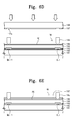
- FIG. 7 is a view showing an exemplary embodiment of laser irradiation apparatus according to the invention.
- a transfer film 119 is laminated on the barrier layer 116 of the first base substrate 111 .
- the transfer film 119 includes a base layer 119 a , and a light-heat conversion layer 119 b disposed on the base layer 119 a .
- An initial water-repellent layer 117 is disposed on the light-heat conversion layer 119 b .
- the base layer 119 a may include at least one polymer material selected from the group consisting of polyester, polyacryl, polyepoxy, polyethylene and polystyrene, or glass.
- the light-heat conversion layer 119 b absorbs the light in the infrared and visible light ranges and partially converts the light into heat.
- the light-heat conversion layer 119 b includes a light absorbing material.
- the light-heat conversion layer 119 b may be a metal layer including one of aluminum (Al), silver (Ag), an oxide a sulfide and a combination thereof, or an organic layer including a polymer of carbon black, graphite or infrared ray dye.
- the metal layer may be formed by a vacuum deposition method, an electron beam deposition method or a sputtering method, and the organic layer may be formed by a gravure coating method, an extrusion coating method, a spin coating method or a knife coating method.
- a laser irradiation apparatus 10 is provided on the transfer film 119 .
- the laser irradiation apparatus 10 includes a light source device 11 , a light valve 12 and an auto-focusing lens 13 .
- the light source device 11 includes a near-infrared ray diode. In one exemplary embodiment, as an example, the light source device 11 outputs a laser beam having a wavelength of about 830 nm.
- the laser beam output from the light source device 11 is provided to the auto-focusing lens 13 through the light valve 12 .
- the light valve 12 blocks the laser beam that travels to unnecessary areas.
- the laser beam passing through the light valve 12 is refracted by the auto-focusing lens 13 and irradiated onto a portion of the base layer 119 a.
- the laser beam irradiated onto the portion of the base layer 119 a is absorbed by the light-heat conversion layer 119 b , and then converted into heat energy. Due to the absorbed heat energy, the light-heat conversion layer 119 b pushes a portion of the initial water-repellent layer 117 onto the barrier layer 116 . Then, the initial water-repellent layer 117 is broken, and thus the portion of the initial water-repellent layer 117 is transferred to the barrier layer 116 .
- FIGS. 8A to 8D are cross-sectional views showing still another exemplary embodiment of method of manufacturing a display panel according to the invention.
- FIGS. 8A to 8D show the process of forming layers disposed on the first base substrate 111 of the display panel 110 .
- the same reference numerals denote the same elements in FIGS. 6A to 6E , and thus detailed descriptions of the same elements will be omitted.
- the processes performed before forming the pixel electrode PE on the organic insulating layer 114 are the same as those shown in FIGS. 6A and 6B , and thus detailed descriptions of the processes performed before forming the pixel electrode PE on the organic insulating layer 114 are omitted.
- the transfer film 119 is disposed above the barrier layer 116 .
- the water-repellent layer 117 is coated on the lower surface of the transfer film 119 , which faces the barrier layer 116 .
- the water-repellent layer 117 is provided with an opening 117 a formed therethrough to expose the lower surface of the transfer film 119 .
- the laser irradiation apparatus 10 ( FIG. 7 ) is disposed on the transfer film 119 to irradiate the laser onto the transfer film 119 .
- the water-repellent layer 117 formed on the lower surface of the transfer film 119 may be transferred to the barrier layer 116 .
- the water-repellent layer 117 includes the material having the hydrophobic property or a layer of which a surface is modified to have the hydrophobic property.
- the water-repellent layer 117 may be formed directly on the barrier layer 116 .
- the water-repellent layer 117 formed on the barrier layer 116 maintains the opening 117 a formed therethrough to expose the barrier layer 116 .
- the barrier wall 115 is formed on the barrier layer 116 exposed through the opening 117 a of the water-repellent layer 117 .
- the barrier wall 115 defines the storage area RA in each pixel.
- the water-repellent layer 117 may be transferred to a desired position before the barrier wall 115 is formed.
Landscapes
- Physics & Mathematics (AREA)
- General Physics & Mathematics (AREA)
- Optics & Photonics (AREA)
- Nonlinear Science (AREA)
- Health & Medical Sciences (AREA)
- Life Sciences & Earth Sciences (AREA)
- Chemical & Material Sciences (AREA)
- Chemical Kinetics & Catalysis (AREA)
- Electrochemistry (AREA)
- Molecular Biology (AREA)
- Electrochromic Elements, Electrophoresis, Or Variable Reflection Or Absorption Elements (AREA)
Abstract
Description
Claims (14)
Priority Applications (1)
| Application Number | Priority Date | Filing Date | Title |
|---|---|---|---|
| US14/507,423 US9279976B2 (en) | 2012-01-18 | 2014-10-06 | Electrowetting display apparatus and method of manufacturing the same |
Applications Claiming Priority (2)
| Application Number | Priority Date | Filing Date | Title |
|---|---|---|---|
| KR1020120005756A KR101945535B1 (en) | 2012-01-18 | 2012-01-18 | Electrowetting display |
| KR10-2012-0005756 | 2012-01-18 |
Related Child Applications (1)
| Application Number | Title | Priority Date | Filing Date |
|---|---|---|---|
| US14/507,423 Division US9279976B2 (en) | 2012-01-18 | 2014-10-06 | Electrowetting display apparatus and method of manufacturing the same |
Publications (2)
| Publication Number | Publication Date |
|---|---|
| US20130182309A1 US20130182309A1 (en) | 2013-07-18 |
| US8854717B2 true US8854717B2 (en) | 2014-10-07 |
Family
ID=48779776
Family Applications (2)
| Application Number | Title | Priority Date | Filing Date |
|---|---|---|---|
| US13/743,759 Expired - Fee Related US8854717B2 (en) | 2012-01-18 | 2013-01-17 | Electrowetting display apparatus and method of manufacturing the same |
| US14/507,423 Expired - Fee Related US9279976B2 (en) | 2012-01-18 | 2014-10-06 | Electrowetting display apparatus and method of manufacturing the same |
Family Applications After (1)
| Application Number | Title | Priority Date | Filing Date |
|---|---|---|---|
| US14/507,423 Expired - Fee Related US9279976B2 (en) | 2012-01-18 | 2014-10-06 | Electrowetting display apparatus and method of manufacturing the same |
Country Status (2)
| Country | Link |
|---|---|
| US (2) | US8854717B2 (en) |
| KR (1) | KR101945535B1 (en) |
Cited By (3)
| Publication number | Priority date | Publication date | Assignee | Title |
|---|---|---|---|---|
| US20150241689A1 (en) * | 2014-02-25 | 2015-08-27 | Amazon Technologies, Inc. | Electrowetting display structures |
| US9279976B2 (en) * | 2012-01-18 | 2016-03-08 | Amazon Technologies, Inc. | Electrowetting display apparatus and method of manufacturing the same |
| WO2016074550A1 (en) * | 2014-11-14 | 2016-05-19 | Beijing Zhigu Rui Tuo Tech Co., Ltd | Display device with adjustable pixel density and method for adjusting display pixel density |
Families Citing this family (9)
| Publication number | Priority date | Publication date | Assignee | Title |
|---|---|---|---|---|
| KR101963902B1 (en) * | 2012-08-08 | 2019-03-29 | 리쿠아비스타 비.브이. | Electrowetting display device and manufacturing method thereof |
| US9046682B2 (en) * | 2013-11-05 | 2015-06-02 | Amazon Technologies, Inc. | Mechanical stress mitigation in electrowetting display structures |
| US9513474B2 (en) | 2014-02-12 | 2016-12-06 | Amazon Technologies, Inc. | Electrowetting element |
| US9740000B2 (en) * | 2014-12-23 | 2017-08-22 | Amazon Technologies, Inc. | Electrowetting display device with shaped colour filter |
| US9904048B2 (en) * | 2014-12-23 | 2018-02-27 | Amazon Technologies, Inc. | Electrowetting display device with shaped colour filter |
| US9659534B2 (en) * | 2014-12-29 | 2017-05-23 | Amazon Technologies, Inc. | Reducing visual artifacts and reducing power consumption in electrowetting displays |
| CN105093520B (en) * | 2015-08-19 | 2017-10-10 | 华南师范大学 | The preparation method and electrowetting display device of a kind of electrowetting display device substrate |
| KR102261236B1 (en) * | 2018-04-17 | 2021-06-04 | 주식회사 엘지화학 | Partition wall pattern film and method for manufacturing thereof |
| JP7501827B2 (en) | 2019-09-04 | 2024-06-18 | イー インク コーポレイション | Display device substrate, display device, electronic device, and method for manufacturing display device substrate |
Citations (11)
| Publication number | Priority date | Publication date | Assignee | Title |
|---|---|---|---|---|
| KR100782466B1 (en) | 2006-05-22 | 2007-12-05 | 삼성에스디아이 주식회사 | laser irradiation device and fabrication method of organic light emitting display device using the same |
| KR20080002201A (en) | 2006-06-30 | 2008-01-04 | 엘지.필립스 엘시디 주식회사 | Electro wetting display device |
| KR20090071111A (en) | 2007-12-27 | 2009-07-01 | 엘지디스플레이 주식회사 | Transfer substrate and method of manufacturing organic light emitting diode display device using the same |
| US7746540B2 (en) | 2007-12-28 | 2010-06-29 | Industrial Technology Research Institute | Electrowetting display devices and fabrication methods thereof |
| US7821699B1 (en) | 2009-06-10 | 2010-10-26 | Industrial Technology Research Institute | Electrowetting display and method for fabricating the same |
| US20110127507A1 (en) | 2009-11-27 | 2011-06-02 | Samsung Mobile Display Co., Ltd. | Method of manufacturing organic light emitting display apparatus, surface treatment device for organic light emitting display apparatus, and organic light emitting display apparatus |
| KR101055697B1 (en) | 2009-08-06 | 2011-08-11 | 한국과학기술원 | Pattern Transfer Method |
| US8599465B2 (en) * | 2010-09-23 | 2013-12-03 | Incha Hsieh | Method for making an electrowetting device |
| US20130329274A1 (en) * | 2012-06-08 | 2013-12-12 | Samsung Display Co., Ltd. | Electrowetting display and method of manufacturing the same |
| US20130335804A1 (en) * | 2012-06-14 | 2013-12-19 | Samsung Display Co., Ltd. | Electrowetting display device and method of manufacturing the same |
| US8654428B2 (en) * | 2011-05-26 | 2014-02-18 | Boe Technology Group Co., Ltd. | Electrowetting display unit and electrowetting display device |
Family Cites Families (3)
| Publication number | Priority date | Publication date | Assignee | Title |
|---|---|---|---|---|
| JP2008170631A (en) * | 2007-01-10 | 2008-07-24 | Sony Corp | Liquid device, and device and method for manufacturing liquid device |
| US7763314B2 (en) * | 2008-01-29 | 2010-07-27 | Motorola, Inc. | Forming an electrowetting module having a hydrophilic grid |
| KR101945535B1 (en) * | 2012-01-18 | 2019-02-08 | 리쿠아비스타 비.브이. | Electrowetting display |
-
2012
- 2012-01-18 KR KR1020120005756A patent/KR101945535B1/en active IP Right Grant
-
2013
- 2013-01-17 US US13/743,759 patent/US8854717B2/en not_active Expired - Fee Related
-
2014
- 2014-10-06 US US14/507,423 patent/US9279976B2/en not_active Expired - Fee Related
Patent Citations (12)
| Publication number | Priority date | Publication date | Assignee | Title |
|---|---|---|---|---|
| KR100782466B1 (en) | 2006-05-22 | 2007-12-05 | 삼성에스디아이 주식회사 | laser irradiation device and fabrication method of organic light emitting display device using the same |
| KR20080002201A (en) | 2006-06-30 | 2008-01-04 | 엘지.필립스 엘시디 주식회사 | Electro wetting display device |
| KR20090071111A (en) | 2007-12-27 | 2009-07-01 | 엘지디스플레이 주식회사 | Transfer substrate and method of manufacturing organic light emitting diode display device using the same |
| US7746540B2 (en) | 2007-12-28 | 2010-06-29 | Industrial Technology Research Institute | Electrowetting display devices and fabrication methods thereof |
| US20100223779A1 (en) | 2007-12-28 | 2010-09-09 | Industrial Technology Research Institute | Electrowetting display devices and fabrication methods thereof |
| US7821699B1 (en) | 2009-06-10 | 2010-10-26 | Industrial Technology Research Institute | Electrowetting display and method for fabricating the same |
| KR101055697B1 (en) | 2009-08-06 | 2011-08-11 | 한국과학기술원 | Pattern Transfer Method |
| US20110127507A1 (en) | 2009-11-27 | 2011-06-02 | Samsung Mobile Display Co., Ltd. | Method of manufacturing organic light emitting display apparatus, surface treatment device for organic light emitting display apparatus, and organic light emitting display apparatus |
| US8599465B2 (en) * | 2010-09-23 | 2013-12-03 | Incha Hsieh | Method for making an electrowetting device |
| US8654428B2 (en) * | 2011-05-26 | 2014-02-18 | Boe Technology Group Co., Ltd. | Electrowetting display unit and electrowetting display device |
| US20130329274A1 (en) * | 2012-06-08 | 2013-12-12 | Samsung Display Co., Ltd. | Electrowetting display and method of manufacturing the same |
| US20130335804A1 (en) * | 2012-06-14 | 2013-12-19 | Samsung Display Co., Ltd. | Electrowetting display device and method of manufacturing the same |
Cited By (6)
| Publication number | Priority date | Publication date | Assignee | Title |
|---|---|---|---|---|
| US9279976B2 (en) * | 2012-01-18 | 2016-03-08 | Amazon Technologies, Inc. | Electrowetting display apparatus and method of manufacturing the same |
| US20150241689A1 (en) * | 2014-02-25 | 2015-08-27 | Amazon Technologies, Inc. | Electrowetting display structures |
| US9182589B2 (en) * | 2014-02-25 | 2015-11-10 | Amazon Technologies, Inc. | Electrowetting display structures |
| US9829699B1 (en) | 2014-02-25 | 2017-11-28 | Amazon Technologies, Inc. | Electrowetting display structures |
| WO2016074550A1 (en) * | 2014-11-14 | 2016-05-19 | Beijing Zhigu Rui Tuo Tech Co., Ltd | Display device with adjustable pixel density and method for adjusting display pixel density |
| US10304373B2 (en) | 2014-11-14 | 2019-05-28 | Beijing Zhigu Rui Tuo Tech Co., Ltd. | Display device with adjustable pixel density and method for adjusting display pixel density |
Also Published As
| Publication number | Publication date |
|---|---|
| US9279976B2 (en) | 2016-03-08 |
| KR101945535B1 (en) | 2019-02-08 |
| KR20130084857A (en) | 2013-07-26 |
| US20150022875A1 (en) | 2015-01-22 |
| US20130182309A1 (en) | 2013-07-18 |
Similar Documents
| Publication | Publication Date | Title |
|---|---|---|
| US9279976B2 (en) | Electrowetting display apparatus and method of manufacturing the same | |
| US8885243B2 (en) | Electrowetting display device and method of manufacturing the same | |
| US8514479B2 (en) | Electro-wetting display | |
| US9459444B2 (en) | Electrowetting display device with light absorbing partition walls | |
| US10001638B2 (en) | Electrowetting display device | |
| TWI576626B (en) | Display device | |
| US20140376079A1 (en) | Electrowetting display device | |
| US8059329B2 (en) | Display substrate and method of manufacturing the same | |
| US8259260B2 (en) | Reflective display devices and methods of manufacturing the same | |
| US9064463B2 (en) | Electrowetting display device | |
| US20140002777A1 (en) | Reflective liquid crystal displays and methods of fabricating the same | |
| US9261725B2 (en) | Liquid crystal display and manufacturing method thereof | |
| US20130301106A1 (en) | Electrowetting display panel and method of manufacturing the same | |
| US20080278435A1 (en) | Display device and method of manufacturing the same | |
| US20150022566A1 (en) | Color display device | |
| US9778455B2 (en) | Display apparatus and method of driving the same | |
| CN111025622B (en) | Electrowetting display panel and 3D printing system | |
| CN105654858A (en) | Double-sided display, TFT (thin film transistor) array substrate thereof and array substrate manufacturing method | |
| KR20080086688A (en) | Liquid crystal display device and fabricating method thereof | |
| KR102038532B1 (en) | Display device and method of manufacturing the same | |
| US11921383B2 (en) | Liquid crystal display device and method for operating the same | |
| US9728675B2 (en) | Display substrate, method of manufacturing the same and electro-wetting display panel having the same | |
| KR101858546B1 (en) | Electrofluicid display device | |
| WO2023216160A1 (en) | Display panel, display module, and display device | |
| JP2010032835A (en) | Matrix type display device |
Legal Events
| Date | Code | Title | Description |
|---|---|---|---|
| AS | Assignment |
Owner name: SAMSUNG DISPLAY CO., LTD., KOREA, REPUBLIC OF Free format text: ASSIGNMENT OF ASSIGNORS INTEREST;ASSIGNORS:KIM, DONGHWAN;KIM, SANGIL;CHA, TAEWOON;AND OTHERS;REEL/FRAME:029659/0795 Effective date: 20130114 |
|
| AS | Assignment |
Owner name: SAMSUNG LCD NETHERLANDS R&D CENTER B.V., NETHERLAN Free format text: ASSIGNMENT OF ASSIGNORS INTEREST;ASSIGNOR:SAMSUNG DISPLAY CO., LTD;REEL/FRAME:030636/0260 Effective date: 20130429 |
|
| AS | Assignment |
Owner name: LIQUAVISTA B.V., NETHERLANDS Free format text: ASSIGNMENT OF ASSIGNORS INTEREST;ASSIGNOR:SAMSUNG LCD NETHERLANDS R&D CENTER B.V. (SNRC);REEL/FRAME:030873/0604 Effective date: 20130429 |
|
| AS | Assignment |
Owner name: AMAZON TECHNOLOGIES, INC., NEVADA Free format text: BILL OF SALE;ASSIGNOR:LIQUAVISTA B.V.;REEL/FRAME:033792/0968 Effective date: 20131004 |
|
| STCF | Information on status: patent grant |
Free format text: PATENTED CASE |
|
| MAFP | Maintenance fee payment |
Free format text: PAYMENT OF MAINTENANCE FEE, 4TH YEAR, LARGE ENTITY (ORIGINAL EVENT CODE: M1551) Year of fee payment: 4 |
|
| FEPP | Fee payment procedure |
Free format text: MAINTENANCE FEE REMINDER MAILED (ORIGINAL EVENT CODE: REM.); ENTITY STATUS OF PATENT OWNER: LARGE ENTITY |
|
| LAPS | Lapse for failure to pay maintenance fees |
Free format text: PATENT EXPIRED FOR FAILURE TO PAY MAINTENANCE FEES (ORIGINAL EVENT CODE: EXP.); ENTITY STATUS OF PATENT OWNER: LARGE ENTITY |
|
| STCH | Information on status: patent discontinuation |
Free format text: PATENT EXPIRED DUE TO NONPAYMENT OF MAINTENANCE FEES UNDER 37 CFR 1.362 |
|
| FP | Lapsed due to failure to pay maintenance fee |
Effective date: 20221007 |