US8854521B2 - Solid-state image sensing device and control method of solid-state image sensing device - Google Patents
Solid-state image sensing device and control method of solid-state image sensing device Download PDFInfo
- Publication number
- US8854521B2 US8854521B2 US13/603,728 US201213603728A US8854521B2 US 8854521 B2 US8854521 B2 US 8854521B2 US 201213603728 A US201213603728 A US 201213603728A US 8854521 B2 US8854521 B2 US 8854521B2
- Authority
- US
- United States
- Prior art keywords
- signal
- transistor
- potential level
- control signal
- potential
- Prior art date
- Legal status (The legal status is an assumption and is not a legal conclusion. Google has not performed a legal analysis and makes no representation as to the accuracy of the status listed.)
- Expired - Fee Related, expires
Links
Images


Classifications
-
- H04N5/3741—
-
- H—ELECTRICITY
- H04—ELECTRIC COMMUNICATION TECHNIQUE
- H04N—PICTORIAL COMMUNICATION, e.g. TELEVISION
- H04N25/00—Circuitry of solid-state image sensors [SSIS]; Control thereof
- H04N25/70—SSIS architectures; Circuits associated therewith
- H04N25/76—Addressed sensors, e.g. MOS or CMOS sensors
-
- H—ELECTRICITY
- H04—ELECTRIC COMMUNICATION TECHNIQUE
- H04N—PICTORIAL COMMUNICATION, e.g. TELEVISION
- H04N25/00—Circuitry of solid-state image sensors [SSIS]; Control thereof
- H04N25/70—SSIS architectures; Circuits associated therewith
- H04N25/76—Addressed sensors, e.g. MOS or CMOS sensors
- H04N25/766—Addressed sensors, e.g. MOS or CMOS sensors comprising control or output lines used for a plurality of functions, e.g. for pixel output, driving, reset or power
-
- H—ELECTRICITY
- H04—ELECTRIC COMMUNICATION TECHNIQUE
- H04N—PICTORIAL COMMUNICATION, e.g. TELEVISION
- H04N25/00—Circuitry of solid-state image sensors [SSIS]; Control thereof
- H04N25/70—SSIS architectures; Circuits associated therewith
- H04N25/76—Addressed sensors, e.g. MOS or CMOS sensors
- H04N25/779—Circuitry for scanning or addressing the pixel array
-
- H04N5/376—
Definitions
- Embodiments described herein relate generally to a solid-state image sensing device and a control method of the solid-state image sensing device.
- a CMOS image sensor which mounts a general column analog-to-digital conversion circuit, includes a pixel array in which a plurality of pixel cells are laid out two-dimensionally, a column analog-to-digital conversion circuit for converting pixel signals into digital signals, and a row selection circuit.
- Each pixel includes a photoelectric conversion element (for example, photodiode) for converting an optical signal from an object into an electrical signal (charge), and a plurality of field effect transistors.
- the row selection circuit selects pixels from which signals are to be read for each row. Then, pixel signals are simultaneously output from a plurality of selected pixels on the selected row onto signal lines. The output pixel signals are converted into digital signals by the column analog-to-digital conversion circuit.
- respective transistors are driven to transfer a charge accumulated in the photoelectric conversion element to a signal detection unit, thus detecting and amplifying a charge amount which is accumulated in the photoelectric conversion element and is transferred to the signal detection unit.
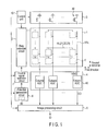
- FIG. 1 is a block diagram showing the overall arrangement of a solid-state image sensing device according to an embodiment
- FIG. 2 is an equivalent circuit diagram showing the arrangement of a pixel of the solid-state image sensing device according to the embodiment
- FIG. 3 is a block diagram showing the arrangement of a solid-state image sensing device according to the first embodiment
- FIG. 4 is a timing chart showing the operation of the solid-state image sensing device according to the first embodiment
- FIG. 5 is a block diagram showing the arrangement of a solid-state image sensing device according to the second embodiment
- FIG. 6 is a timing chart showing the operation of the solid-state image sensing device according to the second embodiment.
- FIG. 7 is a block diagram showing an application example of the solid-state image sensing device according to the embodiment.
- a solid-state image sensing device includes a pixel including a photoelectric conversion element configured to convert light from an object into a signal charge, a signal detection unit to which the signal charge accumulated in the photoelectric conversion element is transferred, a first transistor including one end of a current path connected to the photoelectric conversion element and the other end of the current path connected to the signal detection unit, a second transistor including one end of a current path connected to the signal detection unit and the other end of the current path connected to a control signal line, and a third transistor including a gate connected to the signal detection unit and one end of a current path connected to a signal line from which a pixel signal is output; and a control signal selection circuit configured to select a control signal to be applied to the control signal line.
- the control signal selection circuit sets a potential of the control signal line at a first potential level as the control signal while the pixel signal is read from the pixel, the control signal selection circuit sets the potential of the control signal line at a second potential level as the control signal lower than the first potential level when the pixel is set in an unselected state, and the control signal selection circuit sets the potential of the control signal line at a third potential level as the control signal between the first potential level and the second potential level after the pixel is set in the unselected state.
- a solid-state image sensing device according to the first embodiment will be described below with reference to FIGS. 1 , 2 , 3 , and 4 .
- FIG. 1 shows an example of the overall arrangement of the image sensor of this embodiment.
- the image sensor of this embodiment may be either a front-illuminated image sensor or back-illuminated image sensor.
- the image sensor of this embodiment includes a pixel array 1 , row selection circuit 2 , load circuit 3 , analog-to-digital conversion circuit 4 , image processing circuit 5 , and control unit 10 .
- the pixel array (also referred to as a pixel unit or pixel region hereinafter) 1 includes a plurality of pixels (unit pixels or pixel circuits) 6 .
- the plurality of pixels 6 are arranged in, for example, an m ⁇ n two-dimensional pattern (matrix) along first and second directions.
- the pixel array 1 includes, for example, an effective pixel region and correction pixel region.
- a plurality of pixels 6 arranged along the first direction (row direction) are connected to common row control lines RL.
- Each row control line RL is a control line group including a plurality of control signal lines 21 , 22 , and 23 .
- a plurality of pixels 6 arranged along the second direction (column direction) are connected to common vertical signal lines (also called column control lines) VSL.
- Output signals (referred to as pixel signals or pixel voltages hereinafter) VSIG from the pixels 6 are output onto the vertical signal lines VSL.
- a plurality of (for example, m) row control lines RL are connected to the row selection circuit 2 .
- a plurality of (for example, n) vertical signal lines VSL are connected to the load circuit 3 and analog-to-digital conversion circuit 4 .
- the row selection circuit 2 drives the row control line RL under the control of the control unit 10 to select a plurality of pixels (a row of the pixel array) as read targets connected to the common row control line RL. Also, the row selection circuit 2 sets a plurality of pixels other than read targets in an unselected state (OFF state). Pixels as the read targets will be referred to as selected pixels hereinafter, and those other than the read targets will be referred to as unselected pixels hereinafter.
- the row selection circuit 2 drives the pixels 6 under the control of the control unit 10 to substantially simultaneously output pixel signals VSIG from a plurality of pixels 6 connected to the common row control line RL onto the vertical signal lines VSL to which these pixels 6 are connected.
- the pixel signals VSIG of the pixels for one row connected to the same row control line RL are simultaneously output to the analog-to-digital conversion circuit 4 .
- the row selection circuit 2 supplies control signals required to drive the pixels 6 to the field effect transistors (described later) in the pixels (unit cells or pixel circuits) 6 respectively at predetermined operation timings under the control of the control unit 10 .
- the load circuit 3 includes a plurality of field effect transistors 30 .
- Each field effect transistor 30 in the load circuit 3 will be referred to as a load transistor 30 hereinafter.
- Each load transistor 30 is, for example, an n-channel field effect transistor.
- One end of a current path of the load transistor 30 is connected to one end of the corresponding vertical signal line VSL.
- the other end of the current path of the load transistor 30 is connected to the ground terminal.
- a bias voltage BIAS is applied to the gate of the load transistor 30 .
- the load transistor 30 functions as a constant current source.
- the analog-to-digital conversion circuit 4 is connected to the other end of each of the vertical signal lines VSL.
- the analog-to-digital conversion circuit 4 is a column analog-to-digital conversion circuit.
- the analog-to-digital conversion circuit 4 includes a plurality of column analog-to-digital converters (ADCs) 40 .
- the column ADCs (conversion units) 40 are arranged in correspondence with the respective vertical signal lines VSL, and one column ADC 40 is connected to one vertical signal line VSL.
- the analog-to-digital conversion circuit 4 includes sample-and-hold circuits (not shown) used to sample the pixel signals VSIG.
- the analog-to-digital conversion circuit 4 applies signal processing to analog pixel signals using the column ADCs 40 to convert the analog pixel signals VSIG into digital signals (digital data) D out .
- the digital data D out which is the result of digitization by the column analog-to-digital conversion circuit 4 and corresponds to the pixels 6 for one row, is output to the subsequent image processing circuit 5 .
- the image processing circuit 5 applies correction processing and feature amount calculation processing to the input digital data D out in synchronism with the control of the control unit 10 to form image data for one frame of the pixel array 1 , and outputs that image data to a display device (for example, a display).
- a display device for example, a display
- FIG. 2 is an equivalent circuit diagram showing the internal arrangement of the pixel 6 .
- a plurality of pixels 6 are connected to one vertical signal line VSL.
- the image sensor of this embodiment is, for example, a CMOS image sensor.
- each pixel 6 of the CMOS image sensor includes, for example, one photoelectric conversion element 60 , a signal detection unit 64 , and a plurality of transistors 61 , 62 , and 63 .
- the signal detection unit 64 is formed by a connection node of the transistors 61 and 62 .
- the signal detection unit 64 is, for example, a diffusion layer (impurity semiconductor layer) formed in a semiconductor substrate.
- the signal detection unit 64 formed of the diffusion layer is called a floating diffusion (FD).
- the photoelectric conversion element 60 is, for example, a photodiode 60 .
- the anode of the photodiode 60 is connected to the ground terminal.
- the cathode of the photodiode 60 is connected to the floating diffusion 64 via a current path of the transistor 61 .
- the photodiode 60 can accumulate a charge (signal charge, accumulated charge) generated inside itself according to an intensity of incident light (light coming from an object).
- the pixel 6 includes, for example, the read transistor 61 , reset transistor 62 , and amplifier transistor 63 .
- the read transistor 61 is, for example, an n-channel MOS transistor. One end of a current path of the read transistor 61 is connected to the cathode of the photodiode 60 . The other end of the current path of the read transistor 61 is connected to the floating diffusion 64 . The other end of the current path of the read transistor 61 is connected to one end of a current path of the reset transistor 62 and the gate of the amplifier transistor 63 via the floating diffusion 64 .
- a control signal READ is input to the gate of the read transistor 61 .
- An ON/OFF state of the read transistor 61 is controlled by control signal. READ.
- the read transistor 61 When a signal corresponding to a charge generated by the photodiode 60 of each pixel 6 is output onto the vertical signal line VSL as an output signal VSIG from the pixel 6 , the read transistor 61 is turned on in response to control signal READ. A signal charge from the photodiode 60 is transferred to the floating diffusion 64 via the current path (channel, inversion layer) of the read transistor 61 in the ON state. A voltage corresponding to the charge transferred to the floating diffusion 64 is detected and amplified by the transistor 63 in the pixel 6 , and a voltage (referred to as a signal voltage VPD hereinafter) corresponding to the charge generated by the photodiode 60 is output onto the vertical signal line VSL as the pixel signal VSIG.
- VPD signal voltage
- control signal line also referred to as a read control line hereinafter
- READ a control signal supplied from the row selection circuit 2 to the respective read transistors 61 .
- the reset transistor 62 is, for example, an n-channel MOS transistor. One end (source) of a current path of the reset transistor 62 is connected to the floating diffusion 64 . The other end (drain) of the current path of the reset transistor 62 is connected to a control signal line (or control terminal) 23 to which a control signal RSTDRN is supplied.
- a control signal RESET is input to the gate of the reset transistor 62 .
- An ON/OFF state of the reset transistor 62 is controlled by control signal RESET.
- the reset transistor 62 resets a potential state of the floating diffusion 64 .
- the reset transistor 62 is turned on in response to control signal RESET.
- a voltage (or current) according to control signal RSTDRN is applied to the floating diffusion 64 via the current path of the field-effect transistor 62 in the ON state, thereby resetting a potential of the floating diffusion 64 .
- the potential of the floating diffusion 64 which has received control signal RSTDRN, is detected and amplified by the amplifier transistor 63 in the pixel 6 , and a voltage (referred to as a reset voltage VRST hereinafter) of the floating diffusion 64 in a reset state is output onto the vertical signal line VSL as the output signal VSIG from the pixel 6 .
- a reset voltage VRST a voltage of the floating diffusion 64 in a reset state is output onto the vertical signal line VSL as the output signal VSIG from the pixel 6 .
- the gates of the reset transistors 62 of a plurality of pixels 6 are commonly connected to a control signal line (also referred to as a reset control line hereinafter) 22 via which control signal RESET (also referred to as a reset control signal hereinafter) is supplied.
- RESET also referred to as a reset control signal hereinafter
- one end (drain) of each of the current paths of the reset transistors 62 of the plurality of pixels 6 is commonly connected to the control signal line (also referred to as a reset drain control line hereinafter) 23 to which control signal RSTDRN (also referred to as a reset drain signal hereinafter) is supplied.
- Control signals RESET and RSTDRN are supplied from the row selection circuit 2 to the respective reset transistors 62 .
- the amplifier transistor 63 is, for example, an n-channel MOS transistor. One end (drain) of a current path of the amplifier transistor 63 is connected to a power supply terminal (or power supply line) VDD. The other end (source) of the current path of the amplifier transistor 63 is connected to the vertical signal line VSL. The gate of the amplifier transistor 63 is connected to the floating diffusion 64 .
- the transistor 63 and load circuit 3 form a source-follower.
- the transistor 63 By applying the potential of the floating diffusion 64 to the gate of the transistor 63 as the source-follower, the transistor 63 detects and amplifies the magnitude of the potential of the floating diffusion 64 . A value obtained by shifting a predetermined voltage from the potential of the floating diffusion 64 is output onto the vertical signal line VSL as the pixel signal VSIG indicating the signal voltage VPD or reset voltage VRST.
- One end (drain) of the current path of the amplifier transistor 63 is not connected to the signal line 23 , to which the reset drain signal RSTDRN is supplied.
- the drain of the amplifier transistor 63 and that of the reset transistor 62 are electrically isolated from each other, and are controlled by different potentials.
- the arrangement of the transistors in the pixel 6 is not limited to the example shown in FIG. 2 , and other circuit arrangements may be adopted.
- a circuit arrangement (unit cell) in which two or more photodiodes 60 may be commonly connected to one floating diffusion, and may share the reset transistor 62 and amplifier transistor 63 may be adopted.
- a transistor (address transistor) used to select each pixel may be further added.
- the signal voltage VPD and reset voltage VRST output from each pixel 6 are converted from analog signals into digital signals by digital counter processing of the analog-to-digital conversion circuit 4 .
- the signal voltage VPD and reset voltage VRST are converted into a digital value D out corresponding to a difference voltage between the signal voltage VPD and reset voltage VRST by correlated double sampling (CDS) by the analog-to-digital conversion circuit 4 .
- CDS correlated double sampling
- the image sensor of this embodiment includes a control signal selection circuit 7 .
- the control signal selection circuit 7 outputs a control signal (potential) required to drive the transistors 61 and 63 in each pixel 6 to that pixel 6 via the row selection circuit 2 .
- the control signal selection circuit 7 outputs the reset drain signal RSTDRN of the reset transistor 62 .
- the control signal selection circuit (also referred to as a reset drain signal selection circuit or potential selection circuit hereinafter) 7 outputs the reset drain signal RSTDRN having a plurality of potentials (levels) to a plurality of pixels 6 connected to the common row control line RL at predetermined operation timings via the row selection circuit 2 in accordance with the operations of these pixels 6 .
- the control signal selection circuit 7 may output the read signal READ of the read transistor 61 and the reset control signal RESET of the reset transistor 62 .
- a potential generation circuit 8 generates a potential having a predetermined magnitude corresponding to the operation of the pixel 6 .
- the potential generation circuit 8 includes a charge pump (booster circuit) 80 required to boost up the power supply voltage VDD.
- the potential generation circuit 8 includes a step-down circuit for stepping down the power supply voltage and a constant voltage source (or constant current source).
- the potential generation circuit 8 transfers potentials (voltages) having different magnitudes to the control signal selection circuit 7 according to the operations of the pixel 6 .
- the control signal selection circuit 7 selects a potential corresponding to the operation of the pixel 6 of a plurality of potentials of different magnitudes generated by the potential generation circuit 8 , and outputs the selected potential to the reset transistor 62 in the pixel 6 as the reset drain signal RSTDRN.
- control signal selection circuit 7 included in the image sensor of this embodiment will be described below with reference to FIG. 3 .
- FIG. 3 shows the internal arrangement of the control signal selection circuit 7 included in the image sensor of this embodiment.
- the control signal selection circuit 7 selects one of potentials (potential levels) of three magnitudes having different magnitudes according to the operations of respective pixels 6 which belong to a common row in the pixel array 1 . Then, the control signal selection circuit 7 outputs the selected potential to the pixels 6 as the reset drain signal RSTDRN.
- a high potential (an H-level potential), a low potential (an L-level potential), and a medium potential (an M-level potential) between high and low are input.
- control signal selection circuit 7 is formed using, for example, two selection units 70 A and 71 A.
- level shifters are used as selection units 70 A and 71 A.
- Each of selection units 70 A and 71 A has two input terminals A 0 and B 0 or A 1 and B 1 , and two values (two potentials) are input to each of selection units 70 A and 71 A.
- Each of selection units 70 A and 71 A has one control terminal SXi or SX and one output terminal Xi or X.
- Each of selection units 70 A and 71 A selects one of potentials input to the two input terminals A 0 and B 0 or A 1 and B 1 based on a control signal (also referred to as a switch signal hereinafter) SW 0 or SW 1 input to control terminal SXi or SX, and outputs the selected potential from output terminal Xi or X.
- a control signal also referred to as a switch signal hereinafter
- SW 0 or SW 1 input to control terminal SXi or SX
- outputs from output terminals Xi and X will be described as outputs Xi and X.
- switch signal SW 0 or SW 1 can assume logical 1 (1 signal) or logical 0 (0 signal).
- logical 1 corresponds to approximately the power supply voltage VDD
- logical 0 corresponds to approximately ground potential GND.
- switch signal SW 0 or SW 1 when switch signal SW 0 or SW 1 is logical 1, a potential input to input terminal A 0 or A 1 of selection unit 70 A or 71 A is selected. On the other hand, when switch signal SW 0 or SW 1 is logical 0, a potential input to input terminal B 0 or B 1 of selection unit 70 A or 71 A is selected.
- Output terminal Xi of selection unit 70 A is connected to input terminal A 1 of selection unit 71 A.
- a terminal (input terminal A 0 in this case) to which the high potential is input will be referred to as a high terminal
- a terminal (input terminal B 1 in this case) to which the low potential is input will be referred to as a low terminal
- a terminal (input terminal B 0 in this case) to which the medium potential is input will be referred to as a medium terminal.
- control signal selection circuit 7 In the control signal selection circuit 7 shown in FIG. 3 , the high potential and medium potential are respectively input to input terminals A 0 and B 0 of selection unit 70 A. Output Xi of selection unit 70 A and the low potential are respectively input to input terminals A 1 and B 1 of selection unit 71 A after selection unit 70 A.
- selection unit 70 A selects one of the high and medium potentials based on switch signal SW 0 to decide an intermediate output Xi in the control signal selection circuit 7 .
- the subsequent selection unit 71 A selects one of the intermediate output Xi and the Low-potential based on switch signal SW 1 , and outputs its output X as the reset drain signal RSTDRN.
- selection unit 70 A selects the high potential as the intermediate output Xi; upon application of switch signal SW 0 at logical 0, it selects the medium potential as the intermediate output Xi.
- selection unit 70 B selects the input intermediate output Xi (high or medium potential) as output X; upon application of switch signal SW 0 at logical 0, it selects the low potential as output X.
- one of the potentials of the three magnitudes is output from the control signal selection circuit 7 as the reset drain signal RSTDRN.
- the reset drain signal RSTDRN of the selected potential is substantially simultaneously supplied to the drains of the reset transistors 62 in the pixels 6 connected to the common row control line (drain signal line 23 ).
- the high potential (first driving potential) used as the reset drain signal RSTDRN is set to be a potential (voltage) higher than the power supply voltage VDD.
- different high potentials are set depending on the specifications of power supply voltages of chips of image sensors, and the high potential can assume a voltage ranging from about 3 to 5V.
- the low potential (second driving potential) used as the reset drain signal RSTDRN is set to be a potential which suffices to turn off the amplifier transistor 63 in the pixel 6 , for example, a voltage smaller than a threshold voltage of the transistor.
- the low potential preferably assumes a magnitude greater than zero (ground potential).
- the low potential greater than zero is generated by the potential generation circuit 8 by regulating the power supply voltage or boosting the ground potential.
- the medium potential (third driving potential, middle potential) used as the reset drain signal RSTDRN is set to be, for example, about the power supply voltage VDD.
- the power supply voltage VDD is about 2.8 to 3.5 V according to the specification of the image sensor.
- the medium potential is not limited to the power supply voltage VDD and may have a magnitude between the power supply voltage VDD and ground voltage GND as long as it is a potential having a middle magnitude between the high and low potentials.
- the magnitude of the high potential may be set to be equal to the power supply voltage VDD and the low potential may be set to ground potential (0 V) according to the specification of the image sensor.
- the high potential is used as the reset drain signal RSTDRN, and the potential of the drain signal line 23 is set to the high potential. That high potential is applied to the drain of the reset transistor 62 .
- the low potential is used as the reset drain signal RSTDRN, and the potential of the drain signal line 23 is set to be the low potential.
- the low potential is applied to the drain of the reset transistor 62 .
- the medium potential is used as the reset drain signal RSTDRN, and the potential of the drain signal line 23 is set to be the medium potential. That medium potential is applied to the drain of the reset transistor 62 .
- a state in which the medium potential is applied to the drain of the reset transistor 62 is called a standby state.
- control signal RSTDRN reset drain signal
- the high potential (a potential greater than or equal to the power supply voltage VDD) is often applied to the drains of the reset transistors during most of a period upon driving the image sensor, so as to speed up the operation of the image sensor.
- VDD power supply voltage
- the reset transistors and amplifier transistors in the pixels 6 are driven by the binary reset drain signal, that is, the high and low potentials like in the general image sensor, the reliability of the image sensor and quality of an image to be formed may deteriorate.
- an application period of the high potential in a certain pixel is shorter than that of the medium potential (standby period) in that pixel.
- the image sensor of this embodiment can suppress degradations of elements due to application of a high potential over a long period.
- the medium potential higher than the low potential is applied to the drain of the reset transistor 62 of each pixel 6 , a potential difference between neighboring pixels can be reduced compared to a case in which the low potential is applied to the reset transistor 62 of the pixel 6 , a charge leakage between neighboring pixels, which share the vertical signal line VSL, can be suppressed from being generated.
- the reliability and image quality of the image sensor can be improved.
- a driving method of the solid-state image sensing device (image sensor) of the first embodiment will be described below with reference to FIG. 4 . Note that the operation of the image sensor of this embodiment will be described in this case using FIGS. 1 , 2 , and 3 as needed.
- FIG. 4 is a timing chart showing the driving method of the image sensor of this embodiment.
- the row selection circuit 2 selects a predetermined row control line RL under the control of the control unit 10 .
- a plurality of pixels 6 connected to the selected row control line RL are activated as read targets.
- the pixels 6 before activation are set in the unselected state, and the reset drain signal RSTDRN of the medium potential (for example, the voltage VDD) is applied to the drains of the reset transistors 62 of the respective pixels 6 , as shown in FIG. 4 .
- the reset drain signal RSTDRN of the medium potential for example, the voltage VDD
- the reset drain signal RSTDRN is set to be changed from the medium potential to the high potential (a magnitude greater than voltage VDD).
- switch signal SW 0 is set to logical 1 and applied to selection unit 70 A.
- Selection unit 70 A to which the high and medium potentials are input selects the high potential as the intermediate output Xi based on applied switch signal SW 0 .
- switch signal SW 1 is set to logical 1 and applied to selection unit 71 A.
- Selection unit 71 A to which the low potential (>0 V) and the high potential as the intermediate output Xi are applied selects the input high potential as output X based on applied switch signal SW 1 .
- the control signal selection circuit 7 selects the high potential as the reset drain signal RSTDRN.
- the potential of the drain signal line 23 is set to be the high potential, and the high potential is applied to the drains of the reset transistors 62 of the selected pixels 6 . Since the high potential is applied to the reset transistors 62 , charge amounts which can be accumulated on the floating diffusions 64 can increase, thus improving the dynamic range of the image sensor.
- the high potential is generated by the potential generation circuit 8 by boosting up the power supply voltage VDD.
- the bias voltage BIAS is applied to the gate of the load transistor 30 .
- the reset control signal RESET of logical 1 is applied to the gate of each reset transistor 62 at time t 1 , thus turning on the reset transistor 62 .
- the high potential is applied to the floating diffusion 64 via the current path of the reset transistor 62 .
- the potential FD of the floating diffusion 64 varies (rises) according to the magnitude of the high potential.
- the amplifier transistor 63 is turned on.
- the read transistor 61 is turned off by the read control signal READ.
- the amplifier transistor 63 and load circuit 3 which form the source-follower, output a value obtained by shifting from the potential of the floating diffusion 64 to a certain potential (constant voltage) onto the vertical signal line VSL as the reset voltage VRST of the pixel 6 .
- the potential (pixel voltage) VSIG of the vertical signal line VSL varies to about the reset voltage VRST.
- the output reset voltage VRST is sampled by the sample-and-hold circuit (not shown) of the subsequent column analog-to-digital conversion circuit 4 at time t 1 , and is input to the column ADC 40 .
- the reset transistor 62 After the reset voltage VRST is sampled (in/after a first read period RA), the reset transistor 62 is turned off. For example, the read control signal READ at logical 1 is applied to the gate of the read transistor 61 at time t 2 , thus turning on the read transistor 61 .
- a signal charge accumulated in the photodiode 60 is transferred to the floating diffusion 64 via the current path of the read transistor 61 in the ON state. Then, the potential FD of the floating diffusion varies (for example, falls) to a potential according to the signal charge transferred from the photodiode 60 .
- the amplifier transistor 63 operates by a driving force according to the potential FD of the floating diffusion 64 .
- the potential according to the transferred signal charge is detected and amplified by the amplifier transistor 63 , and is output onto the vertical signal line VSL as the signal voltage VPD of that pixel.
- the potential VSIG on the vertical signal line VSL varies to about the signal voltage VPD.
- the output signal voltage VPD is sampled by the sample-and-hold circuit at time t 2 , and is input to the column ADC 40 .
- switch signals SW 0 and SW 1 are maintained at logical 1 during a period in which the reset voltage VRST and signal voltage VPD are read. That is, during a read period (sampling period) P 1 of the pixel signals VRST and VPD from each pixel, the high potential is applied to the control signal line 23 , and is applied to the drain of the reset transistor 62 .
- switch signal SW 0 in the control signal selection circuit 7 is controlled to transit from logical 1 to 0, and switch signal SW 1 at logical 0 is input to selection unit 71 A.
- Selection unit 71 A selects the low potential applied to input terminal B 1 as output X based on switch signal SW 1 at logical 0.
- the low potential selected by the control signal selection circuit 7 is set as the reset drain signal RSTDRN, and the potential of the drain signal line 23 is set to be the low potential. Then, the low potential is applied to the drain of the reset transistor 62 .
- the level of switch signal SW 0 to selection unit 70 A can be either logical 1 or 0.
- the reset drain signal RSTDRN is set at the low potential, and the reset transistor 62 is turned on by the reset control signal RESET.
- the potential FD of the floating diffusion 64 is set to be the low potential as the reset drain signal RSTDRN. Since the low potential is a voltage which is low enough to turn off the amplifier transistor 63 (a voltage lower than the threshold voltage of the transistor), the amplifier transistor 63 is set in an OFF set. Since the amplifier transistor 63 is turned off, this pixel 6 substantially becomes an unselected pixel.
- the reset transistor 62 is turned off by the reset control signal RESET.
- the reset drain signal RSTDRN is set at the medium potential (third period P 3 , standby period). More specifically, switch signal SW 0 of at logical 0 is applied to selection unit 70 A, and switch signal SW 1 at logical 1 is applied to selection unit 71 A.
- the medium potential is selected by selection unit 70 A as the intermediate output Xi, and the intermediate output Xi as the medium potential is selected by selection unit 71 A as output X.
- the medium potential is selected as the reset drain signal RSTDRN, and the potential of the drain signal line 23 is set to be the medium potential.
- the medium potential is applied to the unselected pixel. In the unselected pixel, the medium potential is applied to the drain of the reset transistor 62 in the OFF state.
- the sampled reset voltage VRST and signal voltage VPD undergo the digital processing and CDS processing by the column ADC 40 , and is then output as digital data Dout to the subsequent image processing circuit 5 .
- the aforementioned operations are sequentially executed while switching the selected pixels for respective rows.
- the image processing circuit 5 applies correction processing and feature amount calculation processing to the input digital data Dout, thus forming an image for one frame of the pixel array 1 .
- the formed image is output to a display unit (not shown).
- the image sensor of this embodiment drives the pixels 6 and transistors 62 and 63 in the pixels 6 by the ternary control signal (reset drain signal) including the high potential, low potential, and medium potential as a middle potential between the high and low potentials.
- the ternary control signal reset drain signal
- the reliability and image quality of the image sensor can be improved.
- a solid-state image sensing device (image sensor) according to the second embodiment will be described below with reference to FIGS. 5 and 6 . Note that substantially the same components and functions in the second embodiment as those in the image sensor of the first embodiment will be explained as needed.
- the image sensor of the second embodiment is different from that of the first embodiment in the internal arrangement of a control signal selection circuit (reset drain signal selection circuit) 7 .
- FIG. 5 shows the internal arrangement of the control signal selection circuit (reset drain signal selection circuit) 7 in the image sensor according to the second embodiment.
- a low potential and medium potential are respectively applied to input terminals A 0 and B 0 of a selection unit 70 B which selects an intermediate output Xi.
- the intermediate output Xi of the medium or low potential and a high potential are respectively applied to input terminals A 1 and B 1 of a selection unit 71 B which selects an output X.
- selection unit 70 B the medium potential is selected as the intermediate output Xi based on a switch signal SW 0 at logical 1, and the low potential is selected as the intermediate output Xi based on switch signal SW 0 at logical 0.
- selection unit 71 B the high potential is selected as output X based on a switch signal SW 1 at logical 1, and the intermediate output (medium or low potential) Xi is selected as output X based on switch signal SW 1 at logical 0.
- control signal selection circuit 7 included in the image sensor of the second embodiment will be described below with reference to FIGS. 5 and 6 . Note that the operation of the overall image sensor is the same as that in the first embodiment, and a description thereof will not be repeated.
- FIG. 6 is a timing chart for explaining the driving method of the image sensor of this embodiment.
- the high potential (>VDD) is selected as a reset drain signal RSTDRN, and the potential of a drain signal line 23 is set to be the high potential.
- switch signal SW 1 for selection unit 71 B is set to logical 1.
- switch signal SW 0 for selection unit 70 B may be set at either logical 0 or 1.
- the reset drain signal RSTDRN is controlled to transmit from the high potential to the low potential. For this reason, it is preferable to set switch signal SW 0 to logical 0 and to set the intermediate output Xi of selection unit 70 B in a holding state of the low potential substantially simultaneously with setting of switch signal SW 1 to logical 1.
- sampling operations of a reset voltage VRST and signal voltage VPD are started at predetermined timings t 1 and t 2 .
- switch signal SW 0 is maintained at logical 0, and the signal level of switch signal SW 1 is controlled to transit from logical 1 to 0.
- selection unit 71 B selects the low potential as the intermediate output Xi of selection unit 70 B.
- the low potential as output X of selection unit 71 B is supplied to the drain signal line 23 as the reset drain signal RSTDRN.
- the potential of the drain signal line 23 is set to low.
- the low potential is applied to a floating diffusion 64 and the gate of an amplifier transistor 63 via a reset transistor 62 in an ON state.
- the amplifier transistor 63 is turned off, and the pixel 6 is set in the unselected state.
- the signal level of switch signal SW 0 is controlled to transit from logical 0 to 1, and the signal level of switch signal SW 1 is maintained at logical 0.
- selection unit 70 B selects the medium potential as the intermediate output Xi, and selection unit 71 B selects the medium potential as output X. Therefore, the medium potential is set as the reset drain signal RSTDRN, and is applied to the drain signal line 23 and the drain of the reset transistor 62 in the OFF state.
- the control signal selection circuit 7 can select one of potentials of three magnitudes, that is, the high, low, and medium potentials as a control signal (reset drain signal) to be applied to the drain of the reset transistor 62 . Then, the control signal selection circuit 7 can apply the selected potential level to the pixel 6 and transistors in the pixel 6 at predetermined operation timings.
- the image sensor of this embodiment can suppress degradation of elements caused by application of the high potential over a long period and a charge leakage between neighboring pixels caused by application of the low potential, since it applies the medium potential between the high and low potentials to the pixel 6 in place of the high and low potentials during a predetermined period of the driving sequence of the image sensor.
- control signal selection circuit 7 may have an arrangement in which the low and high potentials are input to selection unit 70 A or 70 B used to select the intermediate output Xi, and the intermediate output Xi and the medium potential are input to selection unit 71 A or 71 B used to select output X as the reset drain signal.
- one of the potentials of the three magnitudes can be applied to the pixel 6 based on switch signals SW 0 and SW 1 to selection units 70 A or 70 B and 71 A or 71 B.
- the image sensor and the driving method of the image sensor according to the second embodiment can improve the reliability and image quality of the image sensor as in the first embodiment.
- the solid-state image sensing device (image sensor) of the embodiment is applied to a digital camera or a mobile phone with a camera as a module.
- FIG. 7 is a block diagram showing the application example of the image sensor of this embodiment.
- a camera (or a mobile phone with a camera) 900 including an image sensor 100 of this embodiment includes, for example, an optical lens unit (lens unit) 101 , signal processor (for example, DSP: Digital Signal Processor) 102 , memory 103 , display 104 , and controller 105 in addition to the image sensor 100 .
- signal processor for example, DSP: Digital Signal Processor
- the image sensor 100 converts light from an object into an electrical signal.
- the lens unit 101 focuses light from an object on the image sensor 100 to form an image corresponding to the light from the object on the image sensor 100 .
- the lens unit 101 includes a plurality of lenses, and can mechanically and/or electrically control optical characteristics (for example, a focal length).
- the DSP 102 processes a signal output from the image sensor 100 .
- the DSP 102 forms an image (image data) corresponding to the object based on the signal from the image sensor 100 .
- the memory 103 stores the image data from the DSP 102 .
- the memory 103 can also store externally supplied signals and data.
- the memory 103 may be a memory chip such as DRAM or flash memory incorporated in the camera 900 or a memory card or USB memory detachable from the main body of the camera 900 .
- the display 104 displays image data from the DSP 102 or memory 103 .
- the data from the DSP 101 or memory 103 is still image data or moving image data.
- the controller 105 controls the operations of the components 100 to 104 in the camera.
- the camera 900 including the image sensor 100 of this embodiment can improve image quality of an image to be formed by the aforementioned arrangement and operation of the image sensor 100 .
Landscapes
- Engineering & Computer Science (AREA)
- Multimedia (AREA)
- Signal Processing (AREA)
- Solid State Image Pick-Up Elements (AREA)
- Transforming Light Signals Into Electric Signals (AREA)
Abstract
Description
Claims (20)
Applications Claiming Priority (2)
| Application Number | Priority Date | Filing Date | Title |
|---|---|---|---|
| JP2011-200774 | 2011-09-14 | ||
| JP2011200774A JP5646420B2 (en) | 2011-09-14 | 2011-09-14 | Solid-state imaging device |
Publications (2)
| Publication Number | Publication Date |
|---|---|
| US20130063643A1 US20130063643A1 (en) | 2013-03-14 |
| US8854521B2 true US8854521B2 (en) | 2014-10-07 |
Family
ID=47829550
Family Applications (1)
| Application Number | Title | Priority Date | Filing Date |
|---|---|---|---|
| US13/603,728 Expired - Fee Related US8854521B2 (en) | 2011-09-14 | 2012-09-05 | Solid-state image sensing device and control method of solid-state image sensing device |
Country Status (4)
| Country | Link |
|---|---|
| US (1) | US8854521B2 (en) |
| JP (1) | JP5646420B2 (en) |
| KR (1) | KR101407792B1 (en) |
| CN (1) | CN103002233B (en) |
Cited By (2)
| Publication number | Priority date | Publication date | Assignee | Title |
|---|---|---|---|---|
| US20140269113A1 (en) * | 2013-03-15 | 2014-09-18 | Kabushiki Kaisha Toshiba | Non-volatile semiconductor storage device capable of increasing operating speed |
| US10274612B2 (en) * | 2015-11-13 | 2019-04-30 | Canon Kabushiki Kaisha | Radiation imaging apparatus and photon counting method |
Families Citing this family (4)
| Publication number | Priority date | Publication date | Assignee | Title |
|---|---|---|---|---|
| KR20150029262A (en) * | 2013-09-10 | 2015-03-18 | 삼성전자주식회사 | An image sensor, an image processing system including the same, and an operating method of the same |
| JP2015128253A (en) * | 2013-12-27 | 2015-07-09 | キヤノン株式会社 | Solid-state imaging device and method of driving the same |
| US10694133B2 (en) * | 2018-07-30 | 2020-06-23 | Brillnics, Inc. | Solid-state imaging device, method for driving solid-state imaging device, and electronic apparatus |
| JP7005459B2 (en) * | 2018-09-13 | 2022-01-21 | 株式会社東芝 | Solid-state image sensor |
Citations (6)
| Publication number | Priority date | Publication date | Assignee | Title |
|---|---|---|---|---|
| JPS63299268A (en) | 1987-05-29 | 1988-12-06 | Toshiba Corp | Solid-state image sensing device |
| JP2004343529A (en) | 2003-05-16 | 2004-12-02 | Sony Corp | Solid-state imaging device, driving method thereof, and camera device |
| US20070024726A1 (en) | 2003-09-16 | 2007-02-01 | Tetsuo Nomoto | Solid-state imaging device and camera system |
| JP2009182992A (en) | 2002-04-04 | 2009-08-13 | Sony Corp | Driving method of solid-state imaging device |
| US20100264298A1 (en) * | 2009-04-17 | 2010-10-21 | Canon Kabushiki Kaisha | Photo-electric conversion device and image capturing system |
| US20110013065A1 (en) * | 2009-07-16 | 2011-01-20 | Canon Kabushiki Kaisha | Solid-state imaging apparatus and driving method therefor |
Family Cites Families (3)
| Publication number | Priority date | Publication date | Assignee | Title |
|---|---|---|---|---|
| JPH0955887A (en) * | 1995-08-15 | 1997-02-25 | Nikon Corp | Photoelectric conversion device and solid-state imaging device using the same |
| JP3466886B2 (en) * | 1997-10-06 | 2003-11-17 | キヤノン株式会社 | Solid-state imaging device |
| JP5238673B2 (en) * | 2009-11-09 | 2013-07-17 | 株式会社東芝 | Solid-state imaging device |
-
2011
- 2011-09-14 JP JP2011200774A patent/JP5646420B2/en not_active Expired - Fee Related
-
2012
- 2012-09-05 US US13/603,728 patent/US8854521B2/en not_active Expired - Fee Related
- 2012-09-13 KR KR1020120101329A patent/KR101407792B1/en not_active Expired - Fee Related
- 2012-09-14 CN CN201210342323.XA patent/CN103002233B/en not_active Expired - Fee Related
Patent Citations (7)
| Publication number | Priority date | Publication date | Assignee | Title |
|---|---|---|---|---|
| JPS63299268A (en) | 1987-05-29 | 1988-12-06 | Toshiba Corp | Solid-state image sensing device |
| JP2009182992A (en) | 2002-04-04 | 2009-08-13 | Sony Corp | Driving method of solid-state imaging device |
| JP2004343529A (en) | 2003-05-16 | 2004-12-02 | Sony Corp | Solid-state imaging device, driving method thereof, and camera device |
| US20070076110A1 (en) | 2003-05-16 | 2007-04-05 | Sony Corporation | Solid-state imaging device, method of driving same, and camera apparatus |
| US20070024726A1 (en) | 2003-09-16 | 2007-02-01 | Tetsuo Nomoto | Solid-state imaging device and camera system |
| US20100264298A1 (en) * | 2009-04-17 | 2010-10-21 | Canon Kabushiki Kaisha | Photo-electric conversion device and image capturing system |
| US20110013065A1 (en) * | 2009-07-16 | 2011-01-20 | Canon Kabushiki Kaisha | Solid-state imaging apparatus and driving method therefor |
Non-Patent Citations (1)
| Title |
|---|
| Office Action issued Jan. 28, 2014 in Japanese Patent Application No. 2011-200774 (with English language translation). |
Cited By (3)
| Publication number | Priority date | Publication date | Assignee | Title |
|---|---|---|---|---|
| US20140269113A1 (en) * | 2013-03-15 | 2014-09-18 | Kabushiki Kaisha Toshiba | Non-volatile semiconductor storage device capable of increasing operating speed |
| US9013926B2 (en) * | 2013-03-15 | 2015-04-21 | Kabushiki Kaisha Toshiba | Non-volatile semiconductor storage device capable of increasing operating speed |
| US10274612B2 (en) * | 2015-11-13 | 2019-04-30 | Canon Kabushiki Kaisha | Radiation imaging apparatus and photon counting method |
Also Published As
| Publication number | Publication date |
|---|---|
| JP5646420B2 (en) | 2014-12-24 |
| US20130063643A1 (en) | 2013-03-14 |
| KR20130029345A (en) | 2013-03-22 |
| JP2013062733A (en) | 2013-04-04 |
| CN103002233A (en) | 2013-03-27 |
| KR101407792B1 (en) | 2014-06-17 |
| CN103002233B (en) | 2016-04-20 |
Similar Documents
| Publication | Publication Date | Title |
|---|---|---|
| US10574925B2 (en) | Solid-state imaging device, method for driving solid-state imaging device, and electronic apparatus | |
| US10257452B2 (en) | Solid-state image pickup apparatus, signal processing method for a solid-state image pickup apparatus, and electronic apparatus | |
| US9479715B2 (en) | Solid-state imaging device, method of driving the same, and electronic system including the device | |
| US9749557B2 (en) | Solid-state image pickup device in which charges overflowing a memory during a charge transfer period are directed to a floating diffusion and method of driving same | |
| US8743252B2 (en) | Solid-state imaging device for high density CMOS image sensor, and driving method thereof | |
| US8816266B2 (en) | Solid-state imaging device, method for driving solid-state imaging device, and electronic apparatus | |
| US9123620B2 (en) | Solid-state image capture device, drive method therefor, and electronic apparatus | |
| US8854521B2 (en) | Solid-state image sensing device and control method of solid-state image sensing device | |
| CN102186024B (en) | Physical quantity detecting device and imaging apparatus | |
| US9172893B2 (en) | Solid-state imaging device and imaging apparatus | |
| WO2018012133A1 (en) | Solid-state imaging device, driving method of solid-state imaging device, and electronic apparatus | |
| WO2018168120A1 (en) | Solid-state imaging device, driving method therefor and electronic apparatus | |
| JP2019532522A (en) | Pixel detection circuit and driving method thereof, image sensor, and electronic device | |
| US12052522B2 (en) | Solid-state imaging apparatus and electronic device | |
| WO2012053127A1 (en) | Solid-state imaging device, driving method therefor, and imaging device | |
| JP5403019B2 (en) | Physical quantity detection apparatus and imaging apparatus | |
| KR20090015286A (en) | Image sensor and its driving method |
Legal Events
| Date | Code | Title | Description |
|---|---|---|---|
| AS | Assignment |
Owner name: KABUSHIKI KAISHA TOSHIBA, JAPAN Free format text: ASSIGNMENT OF ASSIGNORS INTEREST;ASSIGNORS:YAMASHITA, TOMONORI;MATSUURA, TOMOHIRO;SIGNING DATES FROM 20120830 TO 20120904;REEL/FRAME:028898/0699 |
|
| STCF | Information on status: patent grant |
Free format text: PATENTED CASE |
|
| FEPP | Fee payment procedure |
Free format text: PAYOR NUMBER ASSIGNED (ORIGINAL EVENT CODE: ASPN); ENTITY STATUS OF PATENT OWNER: LARGE ENTITY |
|
| MAFP | Maintenance fee payment |
Free format text: PAYMENT OF MAINTENANCE FEE, 4TH YEAR, LARGE ENTITY (ORIGINAL EVENT CODE: M1551) Year of fee payment: 4 |
|
| AS | Assignment |
Owner name: TOSHIBA ELECTRONIC DEVICES & STORAGE CORPORATION, Free format text: ASSIGNMENT OF ASSIGNORS INTEREST;ASSIGNOR:KABUSHIKI KAISHA TOSHIBA;REEL/FRAME:047408/0283 Effective date: 20181026 |
|
| AS | Assignment |
Owner name: NORTH PLATE SEMICONDUCTOR, LLC, MICHIGAN Free format text: ASSIGNMENT OF ASSIGNORS INTEREST;ASSIGNOR:TOSHIBA ELECTRONIC DEVICES & STORAGE CORPORATION;REEL/FRAME:048387/0109 Effective date: 20181213 |
|
| FEPP | Fee payment procedure |
Free format text: MAINTENANCE FEE REMINDER MAILED (ORIGINAL EVENT CODE: REM.); ENTITY STATUS OF PATENT OWNER: LARGE ENTITY |
|
| LAPS | Lapse for failure to pay maintenance fees |
Free format text: PATENT EXPIRED FOR FAILURE TO PAY MAINTENANCE FEES (ORIGINAL EVENT CODE: EXP.); ENTITY STATUS OF PATENT OWNER: LARGE ENTITY |
|
| STCH | Information on status: patent discontinuation |
Free format text: PATENT EXPIRED DUE TO NONPAYMENT OF MAINTENANCE FEES UNDER 37 CFR 1.362 |
|
| FP | Lapsed due to failure to pay maintenance fee |
Effective date: 20221007 |