US8854274B2 - Antenna device with choke sleeve structures - Google Patents
Antenna device with choke sleeve structures Download PDFInfo
- Publication number
- US8854274B2 US8854274B2 US13/236,866 US201113236866A US8854274B2 US 8854274 B2 US8854274 B2 US 8854274B2 US 201113236866 A US201113236866 A US 201113236866A US 8854274 B2 US8854274 B2 US 8854274B2
- Authority
- US
- United States
- Prior art keywords
- ground plane
- choke sleeve
- sleeve structures
- antenna
- unbalanced antenna
- Prior art date
- Legal status (The legal status is an assumption and is not a legal conclusion. Google has not performed a legal analysis and makes no representation as to the accuracy of the status listed.)
- Active, expires
Links
Images


Classifications
-
- H—ELECTRICITY
- H01—ELECTRIC ELEMENTS
- H01Q—ANTENNAS, i.e. RADIO AERIALS
- H01Q1/00—Details of, or arrangements associated with, antennas
- H01Q1/48—Earthing means; Earth screens; Counterpoises
-
- H—ELECTRICITY
- H01—ELECTRIC ELEMENTS
- H01Q—ANTENNAS, i.e. RADIO AERIALS
- H01Q1/00—Details of, or arrangements associated with, antennas
- H01Q1/12—Supports; Mounting means
- H01Q1/22—Supports; Mounting means by structural association with other equipment or articles
- H01Q1/24—Supports; Mounting means by structural association with other equipment or articles with receiving set
- H01Q1/241—Supports; Mounting means by structural association with other equipment or articles with receiving set used in mobile communications, e.g. GSM
- H01Q1/242—Supports; Mounting means by structural association with other equipment or articles with receiving set used in mobile communications, e.g. GSM specially adapted for hand-held use
- H01Q1/243—Supports; Mounting means by structural association with other equipment or articles with receiving set used in mobile communications, e.g. GSM specially adapted for hand-held use with built-in antennas
-
- H—ELECTRICITY
- H01—ELECTRIC ELEMENTS
- H01Q—ANTENNAS, i.e. RADIO AERIALS
- H01Q19/00—Combinations of primary active antenna elements and units with secondary devices, e.g. with quasi-optical devices, for giving the antenna a desired directional characteristic
- H01Q19/02—Details
- H01Q19/021—Means for reducing undesirable effects
-
- H—ELECTRICITY
- H01—ELECTRIC ELEMENTS
- H01Q—ANTENNAS, i.e. RADIO AERIALS
- H01Q9/00—Electrically-short antennas having dimensions not more than twice the operating wavelength and consisting of conductive active radiating elements
- H01Q9/04—Resonant antennas
- H01Q9/30—Resonant antennas with feed to end of elongated active element, e.g. unipole
- H01Q9/40—Element having extended radiating surface
-
- H—ELECTRICITY
- H01—ELECTRIC ELEMENTS
- H01Q—ANTENNAS, i.e. RADIO AERIALS
- H01Q9/00—Electrically-short antennas having dimensions not more than twice the operating wavelength and consisting of conductive active radiating elements
- H01Q9/04—Resonant antennas
- H01Q9/30—Resonant antennas with feed to end of elongated active element, e.g. unipole
- H01Q9/42—Resonant antennas with feed to end of elongated active element, e.g. unipole with folded element, the folded parts being spaced apart a small fraction of the operating wavelength
Definitions
- the invention relates to an antenna, more particularly to a printed circuit board (PCB) antenna.
- PCB printed circuit board
- the invention relates to an antenna, more particularly to a printed circuit board (PCB) antenna.
- PCB printed circuit board
- a PCB antenna 30 commonly used in a small wireless device has an unbalanced structure.
- the unbalanced antenna include a monopole antenna, a Planar Inverted F Antenna, etc. These types of antenna create image currents on the ground plane 32 of the PCB 31 . These image currents will then create standing waves at the ground plane 32 and then can easily create problems such as side lobes and nulls in the radiation pattern of the antenna 30 .
- the problems arise from the designs and structures of the products employing the antenna 30 .
- the components on the PCB 31 are not standardized and the size of the ground plane 32 may vary. When the length of the ground plane 32 is less than one quarter wavelength of the operating frequency, the antenna 30 can have a good omnidirectional radiation pattern commonly seen in dipole antennas.
- the length of the PCB 31 when the length of the PCB 31 is increased to accommodate more components, the length of the ground plane 32 usually exceeds one quarter wavelength of the operating frequency of the antenna 30 . This then causes the image currents on the ground plane 32 to present standing waves and results in the nulls 33 .
- the radiation direction for the antenna 30 will be pointed towards the PCB 31 , causing the radiation pattern of the antenna 30 to have lots of side lobes and nulls. This not only affects the effectiveness of sending and receiving signals, but may also cause some electromagnetic interference to electrical components on the PCB 31 .
- an object of the present invention is to provide an antenna device with choke sleeve structures to improve the radiation pattern of an unbalanced antenna.
- an antenna device comprises a non-conductive substrate, an unbalanced antenna, a ground plane and a pair of choke sleeve structures.
- the non-conductive substrate has one short edge, and two long edges connected respectively to two opposite ends of the short edge and substantially parallel to each other.
- the unbalanced antenna is disposed on the non-conductive substrate proximate to the short edge of the non-conductive substrate, and has a ground portion.
- the ground plane is disposed on the non-conductive substrate, is located at one side of the unbalanced antenna, and is electrically coupled to the ground portion.
- the ground plane has two opposite side edges that extend along the two long edges of the non-conductive substrate.
- the ground plane has a length longer than a quarter of an equivalent wavelength corresponding to an operating frequency of the unbalanced antenna.
- the pair of choke sleeve structures are symmetrically disposed on the ground plane at locations which are spaced apart from the unbalanced antenna by about a quarter of an equivalent wavelength corresponding to the operating frequency.
- Each choke sleeve structure has a first end connected to the ground plane, and a second end extending in a direction away from the unbalanced antenna.
- the choke sleeve structures are symmetrically disposed on the ground plane at locations which are inwardly of the two opposite side edges of the ground plane.
- Each choke sleeve structure is an elongated metal line. There is a first gap between the second end of each of the choke sleeve structures and the ground plane.
- Each of said choke sleeve structures further has an inner side edge, and there is a second gap between the inner side edge and the ground plane.
- the choke sleeve structures are symmetrically disposed on the ground plane at locations which are outwardly of the two opposite side edges of the ground plane.
- Each choke sleeve structure is an elongated metal line and further has an inner side edge forming a gap with the ground plane.
- the choke sleeve structures separate the ground plane into a current active region located at one side of the choke sleeve structures proximate to the unbalanced antenna, a current restricting region where the choke sleeve structures are located, and a current suppressing region located at another side of the choke sleeve structures distal from the unbalanced antenna.
- the choke sleeve structures block the image current on the ground plane from flowing to the current suppressing region. Since the currents of the pair of choke sleeve structures and the neighboring ground plane are the same in magnitude, but opposite in direction, they cancel each other out. Also, by making the length of the current active region shorter than a quarter of an equivalent wavelength corresponding to the operating frequency of the unbalanced antenna, there will not be any nulls inside the current active region.
- the effect of the present invention comes from the incorporation of a pair of choke sleeve structures at the locations approximately a quarter of an equivalent wavelength corresponding to the operating frequency of the unbalanced antenna away from the unbalanced antenna and at two sides of the ground plane of the non-conductive substrate.
- the choke sleeve structures change image current distribution on the ground plane.
- FIG. 1 is a schematic view of a conventional printed circuit board (PCB) antenna
- FIG. 2 illustrates a simulation of image current distribution on a ground plane of the conventional PCB antenna
- FIG. 3 is a schematic view of the first embodiment of an antenna device with a pair of choke sleeve structures according to the present invention
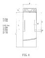
- FIG. 4 is a schematic view to illustrate dimensions of the first embodiment
- FIG. 5 illustrates a simulation of image current distribution on a ground plane of the first embodiment
- FIG. 6 a is a chart showing the radiation pattern on the x-z plane of the first embodiment operating at 2.4 GHz frequency band;
- FIG. 6 b is a chart showing the radiation pattern on the x-y plane of the first embodiment operating at 2.4 GHZ frequency band;
- FIG. 6 c is a chart showing the radiation pattern on the y-z plane of the first embodiment operating at 2.4 GHz frequency band;
- FIG. 7 a is a 3 dimensional chart showing the radiation pattern of the first embodiment operating at 2.4 GHz frequency band
- FIG. 7 b is a section view, with respect to x-z plane, of the 3 dimensional chart shown in FIG. 7 a;
- FIG. 7 c is a section view, with respect to y-z plane, of the 3 dimensional chart shown in FIG. 7 a;
- FIG. 8 is a plot of return loss vs frequency measured for the first embodiment.
- FIG. 9 is a schematic view of the second embodiment of an antenna device with choke sleeve structures according to the present invention.
- the first embodiment of an antenna device of the present invention comprises a non-conductive substrate (for example, the substrate of a printed circuit board) 10 , an unbalanced antenna 11 set up on one end of the non-conductive substrate 10 , and a ground plane 12 that is set up on the other end of the non-conductive substrate 10 and on the same plane as the unbalanced antenna 11 .
- a non-conductive substrate for example, the substrate of a printed circuit board
- an unbalanced antenna 11 set up on one end of the non-conductive substrate 10
- a ground plane 12 that is set up on the other end of the non-conductive substrate 10 and on the same plane as the unbalanced antenna 11 .
- the non-conductive substrate 10 in this embodiment is rectangular in shape, with first and second short edges 101 , 102 arranged substantially parallel to each other, and first and second long edges 103 , 104 arranged substantially parallel to each other and their ends connected to the ends of the short edges 101 , 102 .
- the unbalanced antenna 11 is a one quarter wavelength resonant antenna.
- the unbalanced antenna 11 is disposed on the non-conductive substrate 10 , such as by printing, proximate to the first short edge 101 of the non-conductive substrate 10 .
- the unbalanced antenna 11 has a radiator unit 111 and a ground portion 112 .
- the radiator unit 111 is generally T-shaped, and has an upright portion 113 , and two radiating portions 114 , 115 .
- the two radiating portions 114 , 115 symmetrically extend outwardly from the upright portion 113 proximate to the first short edge 101 toward the two long edges 103 , 104 .
- the ground portion 112 is set up on the other end of the upright portion 113 with respect to the two radiating portions 114 , 115 .
- the ground portion 12 has a centrally disposed feed-in point 116 . Extending symmetrically from the feed-in point 116 toward the first and second long edges 103 and 104 , respectively, are two L-shaped ground sections 117 , 118 .
- the upright portion 113 is coupled electrically to the feed-in point 116 of the ground portion 112 .
- the above description of the unbalanced antenna 11 is considered as an embodiment of the present invention, and this invention is not limited to the disclosed embodiment. Other unbalanced antennas set up on a PCB are suitable for use in this invention.
- the ground plane 12 is set up adjacent to the ground portion 112 of the unbalanced antenna 11 and is coupled electrically to distal ends of the L-shaped ground sections 117 , 118 .
- the ground plane 12 spans the first and second long edges 103 , 104 of the non-conductive substrate 10 and is laid out on a surface of the non-conductive substrate 10 .
- the ground plane 12 has a length longer than one quarter wavelength of the operating frequency (or central frequency) of the unbalanced antenna 11 .
- First and second side edges 121 , 122 of the ground plane 12 are parallel to the first and second long edges 103 , 104 .
- a pair of choke sleeve structures 13 , 14 symmetrically disposed on the ground plane 12 at locations which are inwardly of the two side edges 121 , 122 and which are spaced apart from the unbalanced antenna by the distance of about a quarter of an equivalent wavelength corresponding to the operating frequency (i.e., the distance can be slightly longer or shorter than a quarter of an equivalent wavelength corresponding to the operating frequency).
- the distance between the unbalanced antenna 11 and the pair of choke sleeve structures 13 , 14 is not greater than one quarter wavelength of the operating frequency of the unbalanced antenna 11 .
- each choke sleeve structure 13 , 14 is an elongated metal line section with the length h approximately equal to one equivalent quarter wavelength of the operating frequency of the unbalanced antenna 11 .
- First ends 131 , 141 of the choke sleeve structures 13 , 14 are connected to the ground plane 12 .
- the second ends 132 , 142 of the choke sleeve structures 13 , 14 extend away from the unbalanced antenna 11 .
- Each of said choke sleeve structures 13 , 14 further has an inner side edge 133 , 143 , and there is a second gap g 2 between the inner side edge 133 , 143 and the ground plane 12 . There is no conductive material in the gaps g 1 , g 2 .
- the length h and the first gap g 1 of the choke sleeve structures 13 , 14 can be adjusted to adjust the matching impedance and the radiation pattern while the second gap g 2 can be adjusted to adjust the radiation pattern of the antenna.
- FIG. 4 shows antenna dimensions for operation in the 2.4 GHz frequency band.
- the non-conductive substrate 10 uses FR4 base plate with thickness of 1.6 mm but is not limited to the aforesaid disclosure.
- the choke sleeve structures 13 , 14 separate the ground plane 12 into a current active region located at one side of the choke sleeve structures 13 , 14 proximate to the unbalanced antenna 11 , a current restricting region where the choke sleeve structures 13 , 14 are located, and a current suppressing region located at another side of the choke sleeve structures 13 , 14 distal from the unbalanced antenna 11 .
- the unbalanced antenna 11 is operating at the 2.4 GHz frequency band, it can be seen from FIG.
- the image currents on the ground plane 12 are blocked by the choke sleeve structures 13 , 14 from flowing to the current suppressing region such that the current is very weak in the current suppressing region.
- the strength of the current is strongest at the current restricting region where the choke sleeve structures 13 , 14 are set up. Since the currents of the narrow elongated metal line section of the choke sleeve structures 13 , 14 and the neighboring ground plane 12 are the same in magnitude, but opposite in direction, they cancel each other out, which in turn results in low radiation energy.
- the length of the current active region is not longer than one quarter wavelength of the operating frequency of the unbalanced antenna 11 , there will not be any nulls inside the current active region.
- the radiation patterns shown in FIGS. 6 a to 6 c and 7 a to 7 c can be achieved where the omnidirectional radiation pattern is similar that of the common dipole antenna.
- FIG. 8 shows the result of the measurement of the reflective coefficients of the unbalanced antenna 11 operating at the 2.4 GHz frequency band. From the figure, the 10 dB return loss of the unbalanced antenna 11 has a bandwidth of 385 MHz (2350 MHz-2735 MHz).
- the present invention incorporates a pair of choke sleeve structures 13 , 14 at locations which are approximately a quarter of an equivalent wavelength corresponding to the operating frequency of the unbalanced antenna 11 away from the unbalanced antenna 11 and at two sides of the ground plane 12 of the non-conductive substrate 10 .
- the choke sleeve structures 13 , 14 change image current distribution on the ground plane 12 .
- the choke sleeve structures 13 , 14 are disposed inwardly of the two side edges 121 , 122 of the ground plane 12 , area of the non-conductive substrate 10 is not increased, the choke sleeve structures 13 , 14 do not take up much space on the non-conductive substrate 10 , and the arrangements of the electrical components would not be affected.
- FIG. 9 shows the second embodiment of the present invention.
- the choke sleeve structures 23 , 24 are set up outwardly of the side edges 121 , 122 of the ground plane 12 , and form a respective gap g 2 with the ground plane 12 .
- the rest of the embodiment is set up exactly the same as the first embodiment and is therefore not further described here.
- the choke sleeve structures 23 , 24 cause the same effects as the choke sleeve structures 13 , 14 , by confining the image currents on the ground plane 12 in the current active region above the current restricting area created by the choke sleeve structures 23 , 24 , which alleviates side lobes and nulls of the antenna radiation pattern, causing the unbalanced antenna 11 to have a good omnidirectional radiation pattern and avoiding electrical components on the ground plane 12 from getting electromagnetic interference from the antenna.
- the above embodiments disclose a rectangular PCB set up with the unbalanced antenna 11 and the ground plane 12 .
- the choke sleeve structures 13 , 14 or 23 , 24 made up of narrow elongated metal line sections, and having one end grounded by connecting with the ground plane 12 and the other end extending away from the unbalanced antenna 11 .
- the image currents on the ground plane 12 are restricted in the current restricting region created by the choke sleeve structures 13 , 14 , or 23 , 24 and suppressed at the current suppressing area which is distal from the unbalanced antenna 11 and on the other side of the current restricting region where the choke sleeve structures 13 , 14 or 23 , 24 are installed.
- the electrical components on the PCB do not get electromagnetic interference from the antenna.
Landscapes
- Engineering & Computer Science (AREA)
- Computer Networks & Wireless Communication (AREA)
- Details Of Aerials (AREA)
Abstract
Description
Claims (6)
Applications Claiming Priority (3)
| Application Number | Priority Date | Filing Date | Title |
|---|---|---|---|
| CN201110058891.2A CN102683828B (en) | 2011-03-09 | 2011-03-09 | Antenna assembly with sleeve-shaped choke structures |
| CN201110058891.2 | 2011-03-09 | ||
| CN201110058891 | 2011-03-09 |
Publications (2)
| Publication Number | Publication Date |
|---|---|
| US20120229357A1 US20120229357A1 (en) | 2012-09-13 |
| US8854274B2 true US8854274B2 (en) | 2014-10-07 |
Family
ID=46795056
Family Applications (1)
| Application Number | Title | Priority Date | Filing Date |
|---|---|---|---|
| US13/236,866 Active 2032-08-15 US8854274B2 (en) | 2011-03-09 | 2011-09-20 | Antenna device with choke sleeve structures |
Country Status (2)
| Country | Link |
|---|---|
| US (1) | US8854274B2 (en) |
| CN (1) | CN102683828B (en) |
Families Citing this family (9)
| Publication number | Priority date | Publication date | Assignee | Title |
|---|---|---|---|---|
| TW201424124A (en) * | 2012-12-12 | 2014-06-16 | Realtek Semiconductor Corp | Current breaker and wireless communication device having the same |
| CN104103893A (en) * | 2013-04-11 | 2014-10-15 | 智易科技股份有限公司 | Wide band antenna device |
| JP6183249B2 (en) * | 2014-03-13 | 2017-08-23 | 富士通株式会社 | Wireless device |
| TWI539663B (en) * | 2014-03-19 | 2016-06-21 | 宏碁股份有限公司 | Handheld device |
| TWI587574B (en) * | 2015-07-20 | 2017-06-11 | 廣達電腦股份有限公司 | Mobile device |
| CN108232463B (en) * | 2018-02-28 | 2024-02-27 | 中国人民解放军国防科技大学 | Choke coil for satellite navigation measurement type antenna |
| US20210057818A1 (en) * | 2018-04-25 | 2021-02-25 | Hewlett-Packard Development Company, L.P. | Antennas with in-phase image current |
| CN110752449B (en) * | 2019-11-06 | 2025-02-28 | 合肥联宝信息技术有限公司 | A method for adjusting antenna radiation pattern and terminal equipment |
| CN114744397B (en) * | 2022-06-09 | 2022-11-22 | 荣耀终端有限公司 | Terminal antenna and electronic equipment |
Citations (1)
| Publication number | Priority date | Publication date | Assignee | Title |
|---|---|---|---|---|
| US20090213026A1 (en) * | 2005-10-10 | 2009-08-27 | Laird Technologies Ab | Antenna arrangement provided with a wave trap |
Family Cites Families (4)
| Publication number | Priority date | Publication date | Assignee | Title |
|---|---|---|---|---|
| AU2001280076B2 (en) * | 2000-08-28 | 2007-04-05 | In4Tel Ltd. | Apparatus and method for enhancing low-frequency operation of mobile communication antennas |
| CN101102009B (en) * | 2006-07-03 | 2011-10-05 | 光宝科技股份有限公司 | UWB Antenna Structure |
| CN101304112A (en) * | 2007-05-09 | 2008-11-12 | 光宝科技股份有限公司 | Ultra-wideband antenna and plug-and-play device using same |
| CN101533947B (en) * | 2009-04-16 | 2012-09-05 | 旭丽电子(广州)有限公司 | Doubly-fed antenna |
-
2011
- 2011-03-09 CN CN201110058891.2A patent/CN102683828B/en active Active
- 2011-09-20 US US13/236,866 patent/US8854274B2/en active Active
Patent Citations (1)
| Publication number | Priority date | Publication date | Assignee | Title |
|---|---|---|---|---|
| US20090213026A1 (en) * | 2005-10-10 | 2009-08-27 | Laird Technologies Ab | Antenna arrangement provided with a wave trap |
Also Published As
| Publication number | Publication date |
|---|---|
| CN102683828B (en) | 2015-02-25 |
| US20120229357A1 (en) | 2012-09-13 |
| CN102683828A (en) | 2012-09-19 |
Similar Documents
| Publication | Publication Date | Title |
|---|---|---|
| US8854274B2 (en) | Antenna device with choke sleeve structures | |
| US11431087B2 (en) | Wideband, low profile, small area, circular polarized UHF antenna | |
| KR100683872B1 (en) | Monopole antenna capable of implementing MIO systems | |
| KR101139703B1 (en) | Mimo antenna having multi-isolation element | |
| US9590304B2 (en) | Broadband antenna | |
| US9634387B2 (en) | Multiple-input multiple-output (MIMO) antenna | |
| CN103081220B (en) | Antenna device and wireless communication apparatus | |
| KR20140069968A (en) | Antenna of mobile communication station | |
| KR20120138758A (en) | Antennas with novel current distribution and radiation patterns, for enhanced antenna isolation | |
| US9142884B2 (en) | Antenna device | |
| CN210926318U (en) | Low-profile broadband microstrip antenna based on super surface | |
| US20100253580A1 (en) | Printed antenna and electronic device employing the same | |
| JP4594226B2 (en) | Dual-band patch antenna with slot structure | |
| US20120038534A1 (en) | Loop array antenna system and electronic apparatus having the same | |
| TW201436369A (en) | Multiband hybrid antenna | |
| CN101431179A (en) | Planar Inverted-F Antenna with Extended Ground Plane | |
| US20170170555A1 (en) | Decoupled Antennas For Wireless Communication | |
| US9130276B2 (en) | Antenna device | |
| CN111373603B (en) | Communication device | |
| US20090079659A1 (en) | Multi-mode resonant wideband antenna | |
| KR102363527B1 (en) | Antenna | |
| US7598912B2 (en) | Planar antenna structure | |
| US20080111753A1 (en) | Dual band printed antenna and dual band printed antenna module | |
| TWI473349B (en) | Stand-alone multi-band antenna | |
| US20120235875A1 (en) | Small shorted patch antenna |
Legal Events
| Date | Code | Title | Description |
|---|---|---|---|
| AS | Assignment |
Owner name: LITE-ON TECHNOLOGY CORP., TAIWAN Free format text: ASSIGNMENT OF ASSIGNORS INTEREST;ASSIGNORS:HUNG, TZU-CHIEH;SU, SAOU-WEN;REEL/FRAME:026954/0440 Effective date: 20110908 Owner name: SILITEK ELECTRONIC (GUANGZHOU) CO., LTD., CHINA Free format text: ASSIGNMENT OF ASSIGNORS INTEREST;ASSIGNORS:HUNG, TZU-CHIEH;SU, SAOU-WEN;REEL/FRAME:026954/0440 Effective date: 20110908 |
|
| AS | Assignment |
Owner name: LITE-ON ELECTRONICS (GUANGZHOU) LIMITED, CHINA Free format text: CHANGE OF NAME;ASSIGNOR:SILITEK ELECTRONIC (GUANGZHOU) CO., LTD.;REEL/FRAME:030401/0501 Effective date: 20120731 |
|
| STCF | Information on status: patent grant |
Free format text: PATENTED CASE |
|
| MAFP | Maintenance fee payment |
Free format text: PAYMENT OF MAINTENANCE FEE, 4TH YEAR, LARGE ENTITY (ORIGINAL EVENT CODE: M1551) Year of fee payment: 4 |
|
| FEPP | Fee payment procedure |
Free format text: MAINTENANCE FEE REMINDER MAILED (ORIGINAL EVENT CODE: REM.); ENTITY STATUS OF PATENT OWNER: LARGE ENTITY |
|
| FEPP | Fee payment procedure |
Free format text: 7.5 YR SURCHARGE - LATE PMT W/IN 6 MO, LARGE ENTITY (ORIGINAL EVENT CODE: M1555); ENTITY STATUS OF PATENT OWNER: LARGE ENTITY |
|
| MAFP | Maintenance fee payment |
Free format text: PAYMENT OF MAINTENANCE FEE, 8TH YEAR, LARGE ENTITY (ORIGINAL EVENT CODE: M1552); ENTITY STATUS OF PATENT OWNER: LARGE ENTITY Year of fee payment: 8 |
|
| MAFP | Maintenance fee payment |
Free format text: PAYMENT OF MAINTENANCE FEE, 12TH YEAR, LARGE ENTITY (ORIGINAL EVENT CODE: M1553); ENTITY STATUS OF PATENT OWNER: LARGE ENTITY Year of fee payment: 12 |