US8853519B2 - Thermoelectric conversion device and method of manufacturing the same, and electronic apparatus - Google Patents
Thermoelectric conversion device and method of manufacturing the same, and electronic apparatus Download PDFInfo
- Publication number
- US8853519B2 US8853519B2 US13/116,663 US201113116663A US8853519B2 US 8853519 B2 US8853519 B2 US 8853519B2 US 201113116663 A US201113116663 A US 201113116663A US 8853519 B2 US8853519 B2 US 8853519B2
- Authority
- US
- United States
- Prior art keywords
- semiconductor
- stacked structure
- thermoelectric conversion
- conversion device
- layers
- Prior art date
- Legal status (The legal status is an assumption and is not a legal conclusion. Google has not performed a legal analysis and makes no representation as to the accuracy of the status listed.)
- Active, expires
Links
Images


Classifications
-
- H01L35/26—
-
- H—ELECTRICITY
- H10—SEMICONDUCTOR DEVICES; ELECTRIC SOLID-STATE DEVICES NOT OTHERWISE PROVIDED FOR
- H10N—ELECTRIC SOLID-STATE DEVICES NOT OTHERWISE PROVIDED FOR
- H10N10/00—Thermoelectric devices comprising a junction of dissimilar materials, i.e. devices exhibiting Seebeck or Peltier effects
- H10N10/80—Constructional details
- H10N10/85—Thermoelectric active materials
- H10N10/857—Thermoelectric active materials comprising compositions changing continuously or discontinuously inside the material
-
- H01L35/32—
-
- H—ELECTRICITY
- H10—SEMICONDUCTOR DEVICES; ELECTRIC SOLID-STATE DEVICES NOT OTHERWISE PROVIDED FOR
- H10N—ELECTRIC SOLID-STATE DEVICES NOT OTHERWISE PROVIDED FOR
- H10N10/00—Thermoelectric devices comprising a junction of dissimilar materials, i.e. devices exhibiting Seebeck or Peltier effects
- H10N10/10—Thermoelectric devices comprising a junction of dissimilar materials, i.e. devices exhibiting Seebeck or Peltier effects operating with only the Peltier or Seebeck effects
- H10N10/17—Thermoelectric devices comprising a junction of dissimilar materials, i.e. devices exhibiting Seebeck or Peltier effects operating with only the Peltier or Seebeck effects characterised by the structure or configuration of the cell or thermocouple forming the device
Definitions
- thermoelectric conversion device and a method of manufacturing the same, and an electronic apparatus.
- Thermoelectric conversion devices employing the Seebeck effect can recycle waste heat, and thus have become a focus of attention as an ecologically-friendly energy conservation technique.
- a conventional thermoelectric conversion device has a structure having electrodes made from a conductive material provided on a higher-temperature side insulating material, electrodes made from a conductive material provided on a lower-temperature side insulating material, p-type semiconductor components made from a single material and n-type semiconductor components made from a single material, provided between the electrodes, for example.
- electrodes made from a conductive material provided on a higher-temperature side insulating material electrodes made from a conductive material provided on a lower-temperature side insulating material
- p-type semiconductor components made from a single material
- n-type semiconductor components made from a single material
- thermoelectric conversion device includes: a semiconductor stacked structure including semiconductor layers stacked with each other, the semiconductor layers being made from different semiconductor materials, wherein a material and a composition of each semiconductor layer in the semiconductor stacked structure are selected so as to avoid conduction-band or valence-band discontinuity.
- an electronic apparatus includes: the above-described thermoelectric conversion device; a heat-generating portion; and a cooling portion.
- thermoelectric conversion device includes: forming a semiconductor stacked structure by stacking a first semiconductor layer and a second semiconductor layer alternate over a semiconductor substrate, materials and compositions of the first and second semiconductor layers being selected so as to avoid conduction-band or valence-band discontinuity; and forming an upper electrode over an upper face of the semiconductor stacked structure and forming a lower electrode over a back face of the semiconductor substrate.
- FIG. 1A is a schematic view illustrating the configuration of a thermoelectric conversion device according to a first embodiment
- FIG. 1B is a diagram illustrating the band structure of the semiconductor stacked structure constructing the thermoelectric conversion device in FIG. 1A ;
- FIG. 2A is a schematic cross sectional view illustrating the configuration of the semiconductor stacked structure constructing the thermoelectric conversion device according to the first embodiment
- FIG. 2B is a diagram illustrating the band structure of the semiconductor stacked structure in FIG. 2A ;
- FIG. 3A is a schematic cross sectional view illustrating the configuration of the semiconductor stacked structure constructing a thermoelectric conversion device according to a variant of the first embodiment
- FIG. 3B is a diagram illustrating the band structure of the semiconductor stacked structure in FIG. 3A ;
- FIGS. 4A-4C are schematic cross-sectional views illustrating a method of manufacturing the thermoelectric conversion device according to the first embodiment
- FIG. 5 is a schematic perspective view illustrating the configuration of the thermoelectric conversion device and the method of manufacturing the same according to the first embodiment
- FIG. 6 is a schematic view illustrating the configuration of a thermoelectric conversion device according to a second embodiment
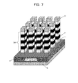
- FIG. 7 is a schematic perspective view illustrating one example of the configuration of the thermoelectric conversion device (having wire-shaped semiconductor stacked structures) according to the second embodiment
- FIG. 8 is a schematic perspective view illustrating another example of the configuration of the thermoelectric conversion device (having mesa-shaped semiconductor stacked structures) according to the second embodiment
- FIG. 9 is a schematic cross-sectional illustrating a method of manufacturing the thermoelectric conversion device according to the second embodiment.
- FIGS. 10A and 10B are schematic cross-sectional views illustrating a method of manufacturing a thermoelectric conversion device according to a variant of the second embodiment
- FIGS. 11A , 11 B and 11 C are schematic cross-sectional views illustrating the method of manufacturing the thermoelectric conversion device according to the variant of the second embodiment
- FIG. 12 is a schematic cross-sectional view illustrating a method of manufacturing a thermoelectric conversion device according to another variant of the second embodiment
- FIG. 13 is a schematic view illustrating a configuration of an electronic apparatus according to a third embodiment.
- FIG. 14 is a schematic view illustrating a configuration of a conventional thermoelectric conversion device.
- thermoelectric conversion devices such as those used for power plants or wrist watches
- middle power ranges ranging from about milli watts to about kilo watts
- thermoelectric conversion devices This is attributed to low conversion efficiencies of such middle-range thermoelectric conversion devices.
- T is the temperature
- ⁇ is the Seebeck coefficient
- ⁇ represents the electrical conductivity
- X represents the thermal conductivity
- m* represents the effective mass
- ⁇ represents the mobility
- the electrical conductivity ⁇ is generally directly proportional to the thermal conductivity X in a conventional thermoelectric material, such as in semiconductor material used in a thermoelectric conversion device.
- the effective mass m* is generally inversely proportional to the mobility ⁇ .
- thermoelectric conversion devices utilizing a conventional single material, resulting in hindering development of thermoelectric conversion devices with higher conversion efficiencies.
- thermoelectric conversion device exhibiting a higher conversion efficiency and an electronic apparatus including such a thermoelectric conversion device.
- thermoelectric conversion device and a method of manufacturing the same according to embodiments will be described with reference to the drawings.
- thermoelectric conversion device and a method of manufacturing the same according to a first embodiment will be described with reference to FIGS. 1A-5 .
- the thermoelectric conversion device includes a semiconductor stacked structure 3 formed by stacking a plurality of semiconductor layers 1 and 2 made from different semiconductor materials, and a positive electrode 4 and a negative electrode 5 provided above and below the semiconductor stacked structure 3 in the stacking direction, respectively, sandwiching the semiconductor stacked structure 3 . That is, the positive electrode 4 is provided above the top of the semiconductor stacked structure, and the negative electrode 5 is provided blow the bottom of the semiconductor stacked structure.
- the semiconductor stacked structure 3 is formed over a semiconductor substrate 6 , and the positive electrode (upper electrode) 4 is formed over the upper face of the semiconductor stacked structure 3 , whereas the negative electrode (lower electrode) 5 is formed over the back face of the semiconductor substrate 6 .
- thermoelectric conversion device is provided between a heat-generating portion (higher-temperature portion) 7 and a cooling portion (heat-radiating portion; lower-temperature portion) 8 , provided in an electronic apparatus, for example. More specifically, the thermoelectric conversion device is provided such that one electrode (positive electrode 4 , in this embodiment) contacts the heat-generating portion 7 while the other electrode (negative electrode 5 , in this embodiment) contacts the cooling portion 8 .
- This configuration provides temperature gradient along the stacking direction of the semiconductor stacked structure 3 . For example, when the heat-generating portion 7 and the cooling portion 8 are located on the top and the bottom of the stacked structure, respectively, temperature gradient is to be provided along a vertical direction.
- each of the semiconductor layers 1 and 2 constructing the semiconductor stacked structure 3 are selected so as to avoid conduction-band discontinuity within the band structure, as depicted in FIG. 1B .
- This configuration prevents carrier electrons from being blocked at the band edges (interfaces) between the semiconductor layers 1 A and 2 A, and thereby facilitating diffusion of the electrons from the plus (+) side to the minus ( ⁇ ) side, resulting in providing favorable electric conduction.
- phonons are scattered at the interfaces between the semiconductor layers 1 A and 2 A, resulting in reducing the thermal conductivity.
- the semiconductor stacked structure 3 formed by stacking a plurality of semiconductor layers 1 A and 2 A made from different semiconductor materials enables thermoelectric conversion devices with a higher conversion efficiency, which has been very difficult to be achieved with conventional natural single material.
- the materials and the compositions are selected so as to avoid conduction-band discontinuity in the present embodiment, this is not limiting.
- the material and the composition of each of the semiconductor layers 1 and 2 constructing the semiconductor stacked structure 3 may be selected so as to avoid valence-band discontinuity.
- each semiconductor layer (here, InGaAsP layer 1 B and InGaAlAs layer 2 B) is preferably p-doped since charge carriers are holes.
- the material and the composition of each of the semiconductor layers 1 and 2 constructing the semiconductor stacked structure 3 may be selected so as to avoid conduction-band and valence-band discontinuities, for example.
- the material and the composition of each of the semiconductor layers 1 and 2 constructing the semiconductor stacked structure 3 may be selected so as to avoid conduction-band or valence-band discontinuity (discontinuity in at least one of the conduction or valence bands).
- the semiconductor stacked structure 3 is formed by staking two semiconductor layers 1 and 2 having different band gaps, alternately in the present embodiment, this is not limiting.
- the semiconductor layers constructing the semiconductor stacked structure do not necessarily have different band gaps.
- the semiconductor stacked structure is not necessarily formed by staking two semiconductor layers alternately, and may be formed by staking semiconductor layers made from two or more different semiconductor materials (semiconductor materials made from different materials or having different compositions), for example.
- the semiconductor layers 1 and 2 constructing the semiconductor stacked structure 3 defines a superlattice structure in the present embodiment, this is not limiting and the semiconductor layers may be thicker and accordingly do not define a superlattice structure. However, forming thinner semiconductor layers to define a superlattice structure is preferred, since more interfaces are defined between semiconductor layers.
- the semiconductor layers 1 and 2 constructing the semiconductor stacked structure 3 are lattice-matched with each other in the present embodiment, this is not limiting and the semiconductor layers constructing the semiconductor stacked structure may be formed from semiconductor materials having different lattice constants.
- the thickness of each semiconductor layer is preferably set to be equal to or smaller than the critical thickness.
- critical thickness is the thickness of a semiconductor layer within which no lattice defect is generated in the semiconductor layer.
- the semiconductor layers 1 ( 1 A and 1 B) and 2 ( 2 A and 2 B) constructing the semiconductor stacked structure 3 have the same thickness in the present embodiment (see FIGS. 1A , 2 A, and 3 A).
- the semiconductor layers 1 and 2 constructing the semiconductor stacked structure 3 may have different thicknesses.
- the InGaAlAs layer 1 A are preferably formed thicker than the InP layer 2 A. More specifically, when the semiconductor stacked structure is formed from a semiconductor layer made from a quaternary compound semiconductor material and a semiconductor layer made from a binary compound semiconductor material, the quaternary compound semiconductor layer is preferably formed thicker than the binary compound semiconductor layer. This configuration can help to reduce the thermal conductivity.
- thermoelectric conversion device a thermoelectric conversion device according to this embodiment.
- a superlattice structure made from InGaAlAs layer 1 A and InP layer 2 A is formed as a semiconductor stacked structure 3 .
- an InP substrate (semiconductor substrate) 6 is provided as a base for forming the superlattice structure 3 thereover.
- an InGaAlAs layer 1 A and an InP layer 2 A are stacked alternately above the InP substrate 6 by metal organic chemical vapor deposition (MOCVD), for example, to form a InP/InGaAlAs superlattice structure (semiconductor stacked structure) 3 .
- MOCVD metal organic chemical vapor deposition
- Material gases of trimethylindium (TMI, indium source), trimethylgallium (TMG, gallium source), trimethylaluminum (TMA, aluminum source), tertiarybutylarsine (TBA, arsenic source), and tertiarybutylphosphine (TBP, phosphorus source) may be used in the MOCVD, for example.
- TMI trimethylindium
- TMG gallium source
- TMA trimethylaluminum
- TSA aluminum source
- TSA tertiarybutylarsine
- TBP tertiarybutylphosphine
- the composition of a wavelength of approximately 1.15 ⁇ m is selected for the InGaAlAs layer 1 A
- the composition of a wavelength of approximately 0.92 ⁇ m is selected for the InP layer 2 A so as to avoid conduction-band discontinuity within the band structure between an InGaAlAs layer 1 A and an InP layer 2 A.
- the layers 1 A and 2 A
- metals e.g., Ti/Au, AuGe/Au and the like
- evaporation for example, as an upper electrode 4 and a lower electrode 5 , respectively, thereby to fabricate a thermoelectric conversion device having the superlattice structure 3 , as depicted in FIG. 5 .
- an InGaAsP layer 1 B and an InGaAlAs layer 2 B are formed alternately above an InP substrate 6 by MOCVD, for example.
- the composition of a wavelength of approximately 1.3 ⁇ m is selected for the InGaAsP layer 1 B, while the composition of a wavelength of approximately 1.0 ⁇ m or lower is selected for the InGaAlAs layer 2 B is selected so as to avoid valence-band discontinuity within the band structure between an InGaAsP layer 1 B and an InGaAlAs layer 2 B.
- the layers 1 B and 2 B are preferably p-doped.
- thermoelectric conversion device and a method of manufacturing the same according to the present embodiment are advantageous in that a thermoelectric conversion device exhibiting a higher conversion efficiency can be achieved.
- thermoelectric conversion device and a method of manufacturing the same according to a second embodiment will be described with reference to FIGS. 6-11C .
- thermoelectric conversion device and the method of manufacturing the same according to the present embodiment are different from those in the above-described first embodiment and variants thereof (see FIGS. 1A and 5 ) in that a plurality of semiconductor stacked structures 3 A in mesa shape (stripe shape) or wire shape (pillar shape) are provided as the semiconductor stacked structures, as depicted in FIGS. 6 , 7 , and 8 .
- interfaces between the semiconductor layers 1 and 2 constructing the semiconductor stacked structure 3 are utilized for increasing phonon scattering in the above-described first embodiment.
- a plurality of mesa- or wire-shaped semiconductor stacked structures 3 A are provided as semiconductor stacked structures, as depicted in FIGS. 6 , 7 , and 8 , in order to increase phonon scattering by utilizing the surfaces (sides) of the semiconductor stacked structures 3 A, in addition to the interfaces between the semiconductor layers 1 and 2 (i.e., to increase the surface areas), thereby attaining a higher figure of merit ZT.
- FIGS. 6 , 7 , and 8 the same elements as in the above-described first embodiment (see FIGS. 1A and 5 ) are referenced by the like reference symbols.
- mesa- or wire-shaped semiconductor stacked structures 3 A extending in the direction of the semiconductor stack have a shortest cross sectional distance of approximately 1 ⁇ m or shorter.
- the term “shortest cross sectional distance” represents the diameter if the cross-sectional shape of the stacked structures is a circle, or the minor axis diameter if the cross-sectional shape is an ellipse, or the length of short side if cross-sectional shape is a square).
- the mesa- or wire-shaped semiconductor stacked structures 3 A are formed by setting the shortest cross sectional distance to be sufficiently small with respect to the height of the stacked structures 3 A (i.e., by setting the shortest cross sectional distance to be equal to or smaller than the height).
- the mesa- or wire-shaped semiconductor stacked structures 3 A preferably have a cross sectional area of approximately 1 ⁇ m 2 or smaller.
- forming wire-shaped semiconductor stacked structures 3 A having a sufficiently small cross sectional area with respect to the height of the stacked structures 3 A i.e., setting the perimeter length of the cross section to be equal to or smaller than the height
- the surface areas increase, resulting in an improvement in the figure of merit ZT.
- a thermoelectric conversion device having wire-shaped semiconductor stacked structures 3 A has a reduced output with respect to device size, and accordingly, is suitable for applications requiring excellent conversion efficiencies but not requiring a higher output.
- the semiconductor stacked structures 3 A have superlattice structures in this embodiment, and a thermoelectric conversion device having such superlattice structures are referred as a thermoelectric conversion device having nanowire superlattices (superlattice wire structures).
- thermoelectric conversion device having an InP/InGaAlAs superlattice structure 3 , an upper electrode 4 , and a lower electrode 5 is fabricated in the manner similar to the above-described first embodiment (see FIGS. 4A-4C and 5 ).
- the InP/InGaAlAs superlattice structure (semiconductor stacked structure) 3 and the upper electrode 4 are processed into a wire shape by etching certain portions of the InP/InGaAlAs superlattice structure 3 and the upper electrode 4 , by means of photolithography and Ar milling or inductively coupled plasma (ICP) dry etching using SiCl 4 , as depicted in FIG. 9 , for example.
- ICP inductively coupled plasma
- certain portions of the InP/InGaAlAs superlattice structures (semiconductor stacked structures) 3 and the upper electrode 4 may be etched to process them into a mesa shape.
- the method of forming the wire-shaped InP/InGaAlAs superlattice structures 3 A is not limited to the one described above, and the following steps may be used alternatively.
- catalyst layers e.g., layers made from Au
- underlying layers base point
- wire-shaped InP/InGaAlAs superlattice structures 3 A thereover in the subsequent steps are formed, by photolithography, at a plurality of predetermined positions on an Si substrate (semiconductor substrate) 6 A, for example.
- an InGaAlAs layer 1 A and an InP layer 2 A are stacked over a plurality of Au layers 9 alternately, by MOCVD, for example, to form a plurality of wire-shaped InP/InGaAlAs superlattice structures (semiconductor stacked structures) 3 .
- TMI trimethylindium
- TMG trimethylgallium
- TMA trimethylaluminum
- TPA tertiarybutylarsine
- TBP tertiarybutylphosphine
- the layers 1 A and 2 A are preferably n-doped.
- a sacrifice layer 10 is formed over the entire surface using a photoresist, for example, and the top surface of each wire-shaped InP/InGaAlAs superlattice structure 3 A is exposed by etching, for example.
- a metal e.g., Ti/Au, AuGe/Au and the like
- a metal e.g., Ti/Au, AuGe/Au and the like
- thermoelectric conversion device having the plurality of wire-shaped InP/InGaAlAs superlattice structures 3 A (see FIG. 6 ) is fabricated.
- the thermoelectric conversion device has the catalyst layer 9 between the semiconductor substrate 6 A and the semiconductor stacked structures 3 A, as depicted in FIG. 11C .
- catalyst layers e.g., layers made from Au
- underlying layers base points
- mesa-shaped InP/InGaAlAs superlattice structures 3 A thereover, may be formed at a plurality of positions.
- wire-shaped InP/InGaAlAs superlattice structures 3 A can be formed similarly.
- a plurality of wire-shaped InGaAsP/InGaAlAs superlattice structures (semiconductor stacked structures) 3 A may be formed by stacking an InGaAsP 2 A and an InGaAlAs 2 B alternately over a plurality of Au layers 9 as catalyst layers by MOCVD, for example, as depicted in FIG. 12 .
- thermoelectric conversion device and a method of manufacturing the same according to the present embodiment are advantageous in that a thermoelectric conversion device exhibiting a higher conversion efficiency can be achieved, like the above-described first embodiment.
- provision of a plurality of mesa- or wire-shaped semiconductor stacked structures 3 A as semiconductor stacked structures enables an even higher figure of merit ZT, resulting in achieving a thermoelectric conversion device exhibiting an even higher conversion efficiency.
- the electronic apparatus includes a CPU chip (heat-generating portion; higher-temperature portion) 21 mounted over a printed circuit board 20 , micro heat pipes (heat-generating portion; higher-temperature portion) 22 provided in contact with the CPU chip 21 , a cooling portion (heat-radiating portion; lower-temperature portion) 23 , and an electricity storage section 24 , for example.
- a CPU chip heat-generating portion; higher-temperature portion
- micro heat pipes heat pipes
- cooling portion heat-radiating portion; lower-temperature portion
- electricity storage section 24 for example.
- thermoelectric conversion device 30 according to any of the above-described first and second embodiments and their variants (see FIGS. 1A , 1 B, and 6 ) is applied to the electronic apparatus. More specifically, as depicted in FIG. 13 , a thermoelectric conversion device 30 according to any of the above-described first and second embodiment and their variants is disposed between the heat-generating portions 21 and 22 and the cooling portion 23 of this electronic apparatus. Thus, this electronic apparatus includes the thermoelectric conversion device 30 according to any of the above-described first and second embodiments and their variants (see FIGS.
- thermoelectric conversion device 30 is disposed between the heat-generating portions 21 and 22 and the cooling portion 23 .
- thermoelectric conversion device 30 is disposed such that one of the upper electrode 4 and the lower electrode 5 (see FIGS. 1A , 1 B, and 6 ) of the thermoelectric conversion device 30 contacts the heat-generating portions 21 and 22 in the electronic apparatus, while the other electrode contacts the cooling portion 23 in the electronic apparatus.
- This configuration provides temperature gradient along the stacking direction of the semiconductor stacked structure(s).
- temperature gradient is to be provided along a vertical direction.
- thermoelectric conversion device 30 The description of the rest of configuration of the thermoelectric conversion device 30 or the method of manufacturing the same is omitted since they are the same as those in the above-described first and second embodiments and variants thereof.
- the electronic apparatus according to the present embodiment is advantageous in that an electronic apparatus having a thermoelectric conversion device exhibiting a higher conversion efficiency can be achieved, like the above-described first and second embodiments.
- thermoelectric conversion device 30 according to any of the above-described first and second embodiments and their variant (see FIGS. 1A , 1 B, and 6 ) is applied to an electronic apparatus having a CPU chip 21
- the thermoelectric conversion device according to any of the above-described first and second embodiments and their variants can be applied to an electronic apparatus having an electronic device as a heat-generating source, such as high-power high-frequency power amplifiers and driver modules for electric vehicles and so forth.
- the thermoelectric conversion device provides thermoelectric conversion by utilizing the electronic device generating heat.
- thermoelectric conversion device according to any of the above-described first and second embodiments and their variants (see FIGS. 1A , 1 B, and 6 ) can also be applied to an electronic apparatus for utilizing waste heat, such as thermal power plant, server systems, and body temperature, for example.
- the semiconductor layers constructing a semiconductor stacked structure are made from InP/InGaAlAs or InGaAsP/InGaAlAs in the above-described embodiments and their variants, this is not limiting and other combinations of semiconductor layers, such as GaN/InGaN, may be used, for example.
- An appropriate combination of semiconductor layers in a semiconductor stacked structure may be suitably selected depending on the operating temperature range, for example.
- semiconductor layers constructing a semiconductor stacked structure are preferably made from GaN/InGaN.
Landscapes
- Photovoltaic Devices (AREA)
Abstract
Description
ZT=α 2 σT/X
Claims (15)
Applications Claiming Priority (1)
| Application Number | Priority Date | Filing Date | Title |
|---|---|---|---|
| PCT/JP2008/073813 WO2010073391A1 (en) | 2008-12-26 | 2008-12-26 | Thermoelectric conversion element, method for manufacturing thermoelectric conversion element and electronic device |
Related Parent Applications (1)
| Application Number | Title | Priority Date | Filing Date |
|---|---|---|---|
| PCT/JP2008/073813 Continuation WO2010073391A1 (en) | 2008-12-26 | 2008-12-26 | Thermoelectric conversion element, method for manufacturing thermoelectric conversion element and electronic device |
Publications (2)
| Publication Number | Publication Date |
|---|---|
| US20110284049A1 US20110284049A1 (en) | 2011-11-24 |
| US8853519B2 true US8853519B2 (en) | 2014-10-07 |
Family
ID=42287058
Family Applications (1)
| Application Number | Title | Priority Date | Filing Date |
|---|---|---|---|
| US13/116,663 Active 2029-06-12 US8853519B2 (en) | 2008-12-26 | 2011-05-26 | Thermoelectric conversion device and method of manufacturing the same, and electronic apparatus |
Country Status (3)
| Country | Link |
|---|---|
| US (1) | US8853519B2 (en) |
| JP (1) | JP5293748B2 (en) |
| WO (1) | WO2010073391A1 (en) |
Families Citing this family (8)
| Publication number | Priority date | Publication date | Assignee | Title |
|---|---|---|---|---|
| US8957298B2 (en) * | 2010-09-11 | 2015-02-17 | Peter Milon Orem | Apparatus, systems and methods for electrical power generation from heat |
| JP2013541200A (en) * | 2010-09-11 | 2013-11-07 | オレム,ピーター,ミロン | Apparatus, system and method for generating power from heat |
| KR101876947B1 (en) * | 2011-01-25 | 2018-07-10 | 엘지이노텍 주식회사 | Thermoelectric Device using Bulk Material of Nano Structure and Thermoelectric Module having The Same, and Method of Manufacture The Same |
| JP6134653B2 (en) * | 2011-02-28 | 2017-05-24 | フォノニック デバイセズ、インク | Thin-film heterostructure thermoelectric conversion in IIa and IV-VI material systems |
| AT512315B1 (en) * | 2011-12-19 | 2014-05-15 | Eduard Dipl Ing Buzetzki | THERMO-ELECTRIC ELEMENT |
| KR101956278B1 (en) * | 2011-12-30 | 2019-03-11 | 삼성전자주식회사 | Heterogeneous laminate comprising graphene, thermoelectric material, thermoelectric module and thermoelectric apparatus comprising same |
| JP6176319B2 (en) * | 2013-04-11 | 2017-08-09 | 富士通株式会社 | Thermoelectric conversion element |
| JP6478413B2 (en) * | 2016-02-16 | 2019-03-06 | Jfeスチール株式会社 | Catalyst material and method for promoting catalytic reaction using the same |
Citations (10)
| Publication number | Priority date | Publication date | Assignee | Title |
|---|---|---|---|---|
| JPH1070315A (en) | 1996-08-26 | 1998-03-10 | Osaka Gas Co Ltd | Manufacture of thermoelectric material |
| JP2000269561A (en) | 1999-03-19 | 2000-09-29 | Asahi Chem Ind Co Ltd | Composite structure |
| JP2000299504A (en) | 1999-04-13 | 2000-10-24 | Sharp Corp | Semiconductor material and manufacturing method thereof |
| US6323414B1 (en) * | 1996-12-17 | 2001-11-27 | The Regents Of The University Of California | Heterostructure thermionic coolers |
| WO2003032408A1 (en) | 2001-10-05 | 2003-04-17 | Research Triangle Institute | Phonon-blocking, electron-transmitting low-dimensional structures |
| US20040079408A1 (en) * | 2002-10-23 | 2004-04-29 | The Boeing Company | Isoelectronic surfactant suppression of threading dislocations in metamorphic epitaxial layers |
| JP2004193200A (en) | 2002-12-09 | 2004-07-08 | Japan Science & Technology Agency | Super lattice thermoelectric material |
| US20060102224A1 (en) | 2004-10-29 | 2006-05-18 | Mass Institute Of Technology (Mit) | Nanocomposites with high thermoelectric figures of merit |
| JP2006269818A (en) | 2005-03-24 | 2006-10-05 | Aisin Seiki Co Ltd | Thermoelectric semiconductor element, thermoelectric conversion device |
| US20060237710A1 (en) * | 2005-04-20 | 2006-10-26 | Opnext Japan, Inc. | Semiconductor optical device |
-
2008
- 2008-12-26 JP JP2010543723A patent/JP5293748B2/en active Active
- 2008-12-26 WO PCT/JP2008/073813 patent/WO2010073391A1/en not_active Ceased
-
2011
- 2011-05-26 US US13/116,663 patent/US8853519B2/en active Active
Patent Citations (13)
| Publication number | Priority date | Publication date | Assignee | Title |
|---|---|---|---|---|
| JPH1070315A (en) | 1996-08-26 | 1998-03-10 | Osaka Gas Co Ltd | Manufacture of thermoelectric material |
| US6323414B1 (en) * | 1996-12-17 | 2001-11-27 | The Regents Of The University Of California | Heterostructure thermionic coolers |
| JP2000269561A (en) | 1999-03-19 | 2000-09-29 | Asahi Chem Ind Co Ltd | Composite structure |
| JP2000299504A (en) | 1999-04-13 | 2000-10-24 | Sharp Corp | Semiconductor material and manufacturing method thereof |
| JP2005506693A (en) | 2001-10-05 | 2005-03-03 | リサーチ・トライアングル・インスティチュート | Phonon blocking electron transfer low dimensional structure |
| WO2003032408A1 (en) | 2001-10-05 | 2003-04-17 | Research Triangle Institute | Phonon-blocking, electron-transmitting low-dimensional structures |
| US20030099279A1 (en) | 2001-10-05 | 2003-05-29 | Research Triangle Insitute | Phonon-blocking, electron-transmitting low-dimensional structures |
| US20040079408A1 (en) * | 2002-10-23 | 2004-04-29 | The Boeing Company | Isoelectronic surfactant suppression of threading dislocations in metamorphic epitaxial layers |
| JP2004193200A (en) | 2002-12-09 | 2004-07-08 | Japan Science & Technology Agency | Super lattice thermoelectric material |
| US20060102224A1 (en) | 2004-10-29 | 2006-05-18 | Mass Institute Of Technology (Mit) | Nanocomposites with high thermoelectric figures of merit |
| JP2008523579A (en) | 2004-10-29 | 2008-07-03 | マサチューセッツ・インスティチュート・オブ・テクノロジー(エムアイティー) | Nanocomposites with high thermoelectric figure of merit |
| JP2006269818A (en) | 2005-03-24 | 2006-10-05 | Aisin Seiki Co Ltd | Thermoelectric semiconductor element, thermoelectric conversion device |
| US20060237710A1 (en) * | 2005-04-20 | 2006-10-26 | Opnext Japan, Inc. | Semiconductor optical device |
Non-Patent Citations (5)
| Title |
|---|
| A. S. Kindyak, "Nonlinear surface magnetostatic waves in a ferrite semiconductor structure", Technical Physics, vol. 44, No. 6, (1999), pp. 715-717. * |
| Band Parameter Calculator for III-V Compound Semiconductor, Mar. 25, 2007, http://www.ntu.edu.sg/home/etmei/Subpages/Resource%20for%20Download.htm, Available from www.archive.org. * |
| International Search Report for PCT/JP2008/073813, mailed on Feb. 10, 2009. |
| Japanese Office Action dated Feb. 19, 2013, issued in corresponding Japanese Patent Application No. 2010-543723, w/ English translation. |
| S. Sano; "Development of High-Efficiency Thermoelectric Conversion Module System", Engineering Advancement Association of Japan Thermoelectric Power Generation Forum, Oct. 31, 2005. |
Also Published As
| Publication number | Publication date |
|---|---|
| US20110284049A1 (en) | 2011-11-24 |
| JP5293748B2 (en) | 2013-09-18 |
| WO2010073391A1 (en) | 2010-07-01 |
| JPWO2010073391A1 (en) | 2012-05-31 |
Similar Documents
| Publication | Publication Date | Title |
|---|---|---|
| US8853519B2 (en) | Thermoelectric conversion device and method of manufacturing the same, and electronic apparatus | |
| Kim et al. | Overcoming the fundamental light-extraction efficiency limitations of deep ultraviolet light-emitting diodes by utilizing transverse-magnetic-dominant emission | |
| Neufeld et al. | Effect of doping and polarization on carrier collection in InGaN quantum well solar cells | |
| CN102834937B (en) | LED chip with current spreading layer | |
| KR20120032258A (en) | Gallium nitride based semiconductor device and method of manufacturing the same | |
| EP3407374A1 (en) | Power generation device for generating electricity using heat | |
| JP6609109B2 (en) | Thermoelectric conversion element and method for manufacturing the same, thermoelectric power generation device and Peltier device | |
| O'Dwyer et al. | Scientific and technical challenges in thermal transport and thermoelectric materials and devices | |
| Wang et al. | Piezotronics and piezo-phototronics based on a-axis nano/microwires: fundamentals and applications | |
| Alferov | The history and future of semiconductor heterostructures from the point of view of a Russian scientist | |
| US10886747B2 (en) | Power generation element, power generation module, power generation device, and power generation system | |
| EP2609635B1 (en) | Thermoelectric module comprising thermoelectric element doped with nanoparticles and manufacturing method of the same | |
| Liu et al. | Comparative experimental and simulation studies of high-power AlGaN-based 353 nm ultraviolet flip-chip and top-emitting LEDs | |
| Khuili et al. | Improvement of optical properties of Mg doped ZnO by nanostructuring for applications in optoelectronics | |
| US20160072034A1 (en) | Metals-semiconductor nanowire composites | |
| CN101971374A (en) | Radiation-emitting component and method for producing a radiation-emitting component | |
| JP5402214B2 (en) | Thermoelectric conversion element and thermoelectric conversion module | |
| TWI478406B (en) | Device, system and method for generating power from heat | |
| KR101039208B1 (en) | Solar cell with semiconductor bar, method for manufacturing same, and solar cell-thermoelectric element integration module | |
| Scofield et al. | Composite axial/core-shell nanopillar light-emitting diodes at 1.3 μm | |
| US7888162B2 (en) | Method of manufacturing a photoelectronic device | |
| US12046461B2 (en) | Power generation element | |
| US11664182B2 (en) | Electron emitting element and power generation element | |
| RU2455739C2 (en) | Line of laser diodes | |
| US20070053394A1 (en) | Cooling device using direct deposition of diode heat pump |
Legal Events
| Date | Code | Title | Description |
|---|---|---|---|
| AS | Assignment |
Owner name: FUJITSU LIMITED, JAPAN Free format text: ASSIGNMENT OF ASSIGNORS INTEREST;ASSIGNOR:IWAI, TAISUKE;REEL/FRAME:026361/0222 Effective date: 20110506 |
|
| STCF | Information on status: patent grant |
Free format text: PATENTED CASE |
|
| MAFP | Maintenance fee payment |
Free format text: PAYMENT OF MAINTENANCE FEE, 4TH YEAR, LARGE ENTITY (ORIGINAL EVENT CODE: M1551) Year of fee payment: 4 |
|
| MAFP | Maintenance fee payment |
Free format text: PAYMENT OF MAINTENANCE FEE, 8TH YEAR, LARGE ENTITY (ORIGINAL EVENT CODE: M1552); ENTITY STATUS OF PATENT OWNER: LARGE ENTITY Year of fee payment: 8 |
|
| AS | Assignment |
Owner name: TAIWAN SEMICONDUCTOR MANUFACTURING COMPANY, LTD., TAIWAN Free format text: ASSIGNMENT OF ASSIGNORS INTEREST;ASSIGNOR:FUJITSU LIMITED;REEL/FRAME:069454/0333 Effective date: 20240808 |
|
| MAFP | Maintenance fee payment |
Free format text: PAYMENT OF MAINTENANCE FEE, 12TH YEAR, LARGE ENTITY (ORIGINAL EVENT CODE: M1553); ENTITY STATUS OF PATENT OWNER: LARGE ENTITY Year of fee payment: 12 |