US8853076B2 - Self-aligned contacts - Google Patents
Self-aligned contacts Download PDFInfo
- Publication number
- US8853076B2 US8853076B2 US13/607,856 US201213607856A US8853076B2 US 8853076 B2 US8853076 B2 US 8853076B2 US 201213607856 A US201213607856 A US 201213607856A US 8853076 B2 US8853076 B2 US 8853076B2
- Authority
- US
- United States
- Prior art keywords
- metal gate
- aluminum
- gate structure
- design
- metal
- Prior art date
- Legal status (The legal status is an assumption and is not a legal conclusion. Google has not performed a legal analysis and makes no representation as to the accuracy of the status listed.)
- Expired - Fee Related, expires
Links
Images


Classifications
-
- H—ELECTRICITY
- H10—SEMICONDUCTOR DEVICES; ELECTRIC SOLID-STATE DEVICES NOT OTHERWISE PROVIDED FOR
- H10D—INORGANIC ELECTRIC SEMICONDUCTOR DEVICES
- H10D64/00—Electrodes of devices having potential barriers
- H10D64/01—Manufacture or treatment
- H10D64/013—Manufacture or treatment of electrodes having a conductor capacitively coupled to a semiconductor by an insulator
- H10D64/01302—Manufacture or treatment of electrodes having a conductor capacitively coupled to a semiconductor by an insulator the insulator being formed after the semiconductor body, the semiconductor being silicon
- H10D64/01304—Manufacture or treatment of electrodes having a conductor capacitively coupled to a semiconductor by an insulator the insulator being formed after the semiconductor body, the semiconductor being silicon characterised by the conductor
- H10D64/01318—Manufacture or treatment of electrodes having a conductor capacitively coupled to a semiconductor by an insulator the insulator being formed after the semiconductor body, the semiconductor being silicon characterised by the conductor the conductor comprising a layer of alloy material, compound material or organic material contacting the insulator, e.g. TiN
-
- H—ELECTRICITY
- H10—SEMICONDUCTOR DEVICES; ELECTRIC SOLID-STATE DEVICES NOT OTHERWISE PROVIDED FOR
- H10D—INORGANIC ELECTRIC SEMICONDUCTOR DEVICES
- H10D64/00—Electrodes of devices having potential barriers
- H10D64/01—Manufacture or treatment
- H10D64/017—Manufacture or treatment using dummy gates in processes wherein at least parts of the final gates are self-aligned to the dummy gates, i.e. replacement gate processes
-
- H—ELECTRICITY
- H10—SEMICONDUCTOR DEVICES; ELECTRIC SOLID-STATE DEVICES NOT OTHERWISE PROVIDED FOR
- H10D—INORGANIC ELECTRIC SEMICONDUCTOR DEVICES
- H10D64/00—Electrodes of devices having potential barriers
- H10D64/60—Electrodes characterised by their materials
- H10D64/66—Electrodes having a conductor capacitively coupled to a semiconductor by an insulator, e.g. MIS electrodes
- H10D64/667—Electrodes having a conductor capacitively coupled to a semiconductor by an insulator, e.g. MIS electrodes the conductor comprising a layer of alloy material, compound material or organic material contacting the insulator, e.g. TiN workfunction layers
-
- H—ELECTRICITY
- H10—SEMICONDUCTOR DEVICES; ELECTRIC SOLID-STATE DEVICES NOT OTHERWISE PROVIDED FOR
- H10W—GENERIC PACKAGES, INTERCONNECTIONS, CONNECTORS OR OTHER CONSTRUCTIONAL DETAILS OF DEVICES COVERED BY CLASS H10
- H10W20/00—Interconnections in chips, wafers or substrates
- H10W20/01—Manufacture or treatment
- H10W20/031—Manufacture or treatment of conductive parts of the interconnections
- H10W20/069—Manufacture or treatment of conductive parts of the interconnections by forming self-aligned vias or self-aligned contact plugs
-
- H—ELECTRICITY
- H10—SEMICONDUCTOR DEVICES; ELECTRIC SOLID-STATE DEVICES NOT OTHERWISE PROVIDED FOR
- H10D—INORGANIC ELECTRIC SEMICONDUCTOR DEVICES
- H10D64/00—Electrodes of devices having potential barriers
- H10D64/60—Electrodes characterised by their materials
- H10D64/66—Electrodes having a conductor capacitively coupled to a semiconductor by an insulator, e.g. MIS electrodes
- H10D64/68—Electrodes having a conductor capacitively coupled to a semiconductor by an insulator, e.g. MIS electrodes characterised by the insulator, e.g. by the gate insulator
- H10D64/691—Electrodes having a conductor capacitively coupled to a semiconductor by an insulator, e.g. MIS electrodes characterised by the insulator, e.g. by the gate insulator comprising metallic compounds, e.g. metal oxides or metal silicates
Definitions
- the invention relates to semiconductor structures and methods of manufacture and, more particularly, to self-aligned contacts in a metal gate structure and methods of manufacture.
- CMOS Complementary metal-oxide-semiconductor
- microprocessors microcontrollers
- static RAM static RAM
- analog circuits such as image sensors, data converters, and highly integrated transceivers for many types of communication.
- a metal gate electrode is formed on top of a gate dielectric material, e.g., high-k dielectric material, which, in turn, is formed on top of a semiconductor material.
- a gate dielectric material e.g., high-k dielectric material
- Aluminum can be used as the metal gate material, in combination with a workfunction metal acting as a liner.
- a contact can then be formed adjacent to the metal gate material.
- the contact can be, for example, a borderless or self-aligned contact.
- a method comprises forming a metal gate structure having a sidewall structure.
- the method further comprises recessing the metal gate structure and forming a masking material within the recess.
- the method further comprises forming a borderless contact adjacent to the metal gate structure, overlapping the masking material and the sidewall structure.
- a method comprises forming a metal gate structure comprising an aluminum gate electrode, lined with a workfunction metal liner.
- the method further comprises recessing the metal gate structure by oxidizing the aluminum to form Al 2 O 3 , followed by etching of the Al 2 O 3 and workfunction metal liner.
- the method further comprises forming a masking material within the recess.
- the method further comprises forming a borderless contact adjacent to the metal gate structure, overlapping the masking material.
- a structure comprises a metal gate structure comprising an aluminum electrode and a workfunction liner, located between sidewall structure.
- the structure further comprises a blocking material located within a recess formed in the aluminum electrode and the workfunction liner.
- the structure further comprises a borderless contact overlapping the metal gate structure and contacting the sidewall structure and the blocking material.
- a design structure tangibly embodied in a machine readable storage medium for designing, manufacturing, or testing an integrated circuit comprises the structures of the present invention.
- a hardware description language (HDL) design structure encoded on a machine-readable data storage medium comprises elements that when processed in a computer-aided design system generates a machine-executable representation of the semiconductor structures, which comprises the structures of the present invention.
- a method in a computer-aided design system is provided for generating a functional design model of the semiconductor structures. The method comprises generating a functional representation of the structural elements of the semiconductor structures.
- FIGS. 1-5 show structures and respective processing steps in accordance with aspects of the present invention.
- FIG. 6 is a flow diagram of a design process used in semiconductor design, manufacture, and/or test.
- the invention relates to semiconductor structures and methods of manufacture and, more particularly, to self-aligned contacts in a metal gate structure and methods of manufacture. More specifically, the present invention relates to the formation of a borderless or self-aligned contact in a metal gate structure.
- the present invention provides a recess formation process, which will circumvent galvanic effects between a workfunction metal and a metal gate material. After formation of the recess, a masking material can be formed within the recess, which will prevent electrical shorting between the contact and the metal gate, itself. Accordingly, advantageously, the present invention provides a process for preventing gate to contact short through borderless or self-aligned contacts.
- the present invention provides a controlled aluminum wet recess process for self-aligned or borderless contacts.
- the metal gate stack includes an aluminum stack having a TiN layer.
- the recess formation process includes, for example, oxidation of the aluminum, e.g., using hydrogen peroxide (Al 2 O 3 ), followed by a wet etch removal of Al 2 O 3 using a phosphoric/nitric/acetic acid (PNA) mixture.
- PNA phosphoric/nitric/acetic acid
- the PNA mixture will also remove the TiN layer.
- the above steps can be repeated until a desired aluminum recess depth is reached.
- a masking material e.g., nitride, can then be deposited within the recess in order to protect shorting of the aluminum with a contact metal.
- FIG. 1 shows an intermediate structure and respective processing steps in accordance with aspects of the present invention.
- FIG. 1 shows a gate structure, generally represented as reference numeral 10 .
- the gate structure 10 can be an NFET, PFET, a FINFet structure or other conventional replacement gate structure used in a borderless contact configuration, in accordance with aspects of the present invention.
- the gate structure 10 of the present invention can be formed using conventional deposition, lithography and etching processes, either in a gate-first or gate-last process, as should be understood by those of ordinary skill in the art.
- the gate structure 10 can be formed on a substrate 12 .
- the substrate 12 can be any substrate, e.g., silicon.
- An interlevel dielectric layer 14 is formed on the substrate 12 using, for example, conventional deposition methods, e.g., chemical vapor deposition (CVD).
- the interlevel dielectric layer 14 can be, for example, an oxide material.
- a second interlevel dielectric layer 16 is formed, e.g., deposited, on the interlevel dielectric layer 14 .
- the second interlevel dielectric layer 16 can also be an oxide material.
- a gate dielectric material 18 can be formed on the substrate 12 .
- the gate dielectric material 18 is a high-k dielectric material such as, for example, a hafnium oxide or other hafnium based material.
- the gate dielectric material 18 can be deposited using a conventional CVD process.
- the dielectric material 18 can be deposited within a trench formed after removal of the replacement dummy gate (or, alternatively, prior to the formation of the replacement dummy gate).
- the thickness of the gate dielectric material 18 can vary depending on the required device performance.
- a metal liner 20 is formed on the gate dielectric material 18 and sidewall structures 24 .
- the metal liner 20 is a workfunction metal which may be, for example, TiN or TaN; although other workfunction metals are also contemplated by the present invention.
- the metal liner 20 can have a thickness of about 5 nm; although other dimensions are also contemplated by the present invention.
- a metal gate material 22 is then formed on the metal material 20 .
- the metal gate material 22 is Al, having a width of about 6 nm; although other dimensions are also contemplated by the present invention.
- Sidewalls 24 are formed on the metal liner 20 , which may be a nitride material.
- the sidewalls 24 may be formed during dummy gate (replacement gate) processes, e.g., prior to the deposition of the materials 20 , 22 , as should be understood by those of skill in the art.
- aluminum will oxide during subsequent processes, e.g., chemical mechanical planarization processes, to form an aluminum oxide 26 layer (Al 2 O 3 ).
- a recess 28 is formed by etching the materials 20 , 22 (and Al 2 O 3 ) to a depth of about 15 nm to about 45 nm, more preferably about 20 nm to 45 nm, and even more preferably about 20 nm to about 30 nm.
- the metal gate material 22 e.g., Al
- the metal liner 20 e.g., TiN, TaN
- the Al can be completely etched or removed, prior to adequate removal of the workfunction metal 20 .
- Al can etch at a rate 3 ⁇ faster when in contact with TiN.
- a 12 second conventionally known wet etch process will not impact the Al (no etching will result)
- a 30 second conventionally known wet etch process will provide a minimum recess
- a 60 second conventionally known wet etch process can effectively remove all of the Al.
- the etching processes of the present invention which form the recess 26 , are tailored for the materials 20 , 22 .
- Galvanic corrosion is an electrochemical process in which one metal corrodes preferentially to another when both metals are in electrical contact and immersed in a wet etchant; that is, the TiN accelerates the Al recess etching, whereas, the Al slows the TiN etching. Due to this phenomena, selective Al etching becomes very difficult to control, and is affected by progressive increase in surface area of TiN (or TaN), resulting in enhanced aluminum etching.
- the recess 28 is etched using a sequential wet etching process, in order to circumvent the galvanic effect.
- the sequential etching process includes the use of H 2 O 2 solution and Phosphoric/Nitric/Acetic acid (PNA) mixture.
- PNA Phosphoric/Nitric/Acetic acid
- the H 2 O 2 solution will oxidize the Al, thus forming Al 2 O 3 , which, in turn, can be etched together with the metal liner 20 in a more controllable manner using the PNA mixture.
- the present invention contemplates a 20% H 2 O 2 solution followed by the PNA mixture.
- the PNA mixture has a ratio of 30:1:1:150 of Phosphoric/Nitric/Acetic acid and deionized water.
- the present invention contemplates a 20% H 2 O 2 solution at 50° C. for 30 seconds, followed by the PNA mixture.
- the present invention contemplates a 20% H 2 O 2 solution at 50° C. for 30 seconds, followed by the PNA mixture at 50° C. for 30 seconds. This sequence will achieve a recess of both the materials 20 , 22 (e.g., more specifically, Al 2 O 3 and liner 20 ) of about 15 nm.
- the present invention contemplates repetitively using the H 2 O 2 and PNA mixture, until a desired recess depth is achieved.
- the etching process can use the following sequential cycle to achieve a depth of about 30 nm:
- a masking material 30 is formed within the recess (recess 28 ) and on a surface of the interlevel dielectric material 16 .
- the masking material 30 can be, for example, a nitride material which is used to prevent shorting between the metal gate material 22 and subsequent formation of a contact (see, e.g., FIGS. 4 and 5 ).
- the masking material 30 is deposited using, for example, a CVD process or atomic layer deposition (ALD) process. After deposition, the masking material 30 is planarized to remove the material from the interlevel dielectric material 16 , thus forming an exposed planar surface 32 .
- the planarization process can be, for example, a chemical mechanical planarization (CMP) process.
- CMP chemical mechanical planarization
- the masking material 30 will remain within the recess after the CMP process, thus completing a metal gate structure 35 , e.g., gate dielectric material 18 , metal liner 20 , metal gate 22 , masking material 30 and sidewalls 24 .
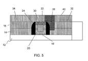
- an interlevel dielectric material 34 is formed over the planar surface 32 of the interlevel dielectric material 16 and the masking material 30 .
- the interlevel dielectric material 34 is an oxide material, which is deposited using, e.g., CVD processes.
- a trench 36 is formed through the interlevel dielectric material 34 , which may extend into the interlevel dielectric materials 14 , 16 .
- the trench 36 overlaps with the metal gate structure 35 , e.g., masking material 30 and sidewalls 26 .
- the trench 36 can be formed using any conventional lithography and etching process, known to those of skill in the art.
- a self-aligned borderless contact 38 is formed within the trench 35 using conventional deposition processes.
- the self-aligned borderless contact 38 is a metal material, e.g., Al or tungsten.
- the self-aligned borderless contact 38 is formed by a deposition process using, for example, CVD or ALD processes; although other deposition processes are also contemplated by the present invention.
- the metal material forming the contact 38 can be planarized to form a planar surface 40 .
- the metal material forming the self-aligned borderless contact 38 does not make any contact (electrical contact) with the metal gate material 22 or the metal liner 20 , as they are protected by the masking material 30 . In this way, a borderless contact can be formed within a metal gate process, which prevents a gate to contact short.
- FIG. 6 is a flow diagram of a design process used in semiconductor design, manufacture, and/or test.
- FIG. 6 shows a block diagram of an exemplary design flow 900 used for example, in semiconductor IC logic design, simulation, test, layout, and manufacture.
- Design flow 900 includes processes, machines and/or mechanisms for processing design structures or devices to generate logically or otherwise functionally equivalent representations of the design structures and/or devices described above and shown in FIGS. 1-5 .
- the design structures processed and/or generated by design flow 900 may be encoded on machine-readable transmission or storage media to include data and/or instructions that when executed or otherwise processed on a data processing system generate a logically, structurally, mechanically, or otherwise functionally equivalent representation of hardware components, circuits, devices, or systems.
- Machines include, but are not limited to, any machine used in an IC design process, such as designing, manufacturing, or simulating a circuit, component, device, or system.
- machines may include: lithography machines, machines and/or equipment for generating masks (e.g., e-beam writers), computers or equipment for simulating design structures, any apparatus used in the manufacturing or test process, or any machines for programming functionally equivalent representations of the design structures into any medium (e.g. a machine for programming a programmable gate array).
- Design flow 900 may vary depending on the type of representation being designed. For example, a design flow 900 for building an application specific IC (ASIC) may differ from a design flow 900 for designing a standard component or from a design flow 900 for instantiating the design into a programmable array, for example a programmable gate array (PGA) or a field programmable gate array (FPGA) offered by Altera® Inc. or Xilinx® Inc.
- ASIC application specific IC
- PGA programmable gate array
- FPGA field programmable gate array
- FIG. 6 illustrates multiple such design structures including an input design structure 920 that is preferably processed by a design process 910 .
- Design structure 920 may be a logical simulation design structure generated and processed by design process 910 to produce a logically equivalent functional representation of a hardware device.
- Design structure 920 may also or alternatively comprise data and/or program instructions that when processed by design process 910 , generate a functional representation of the physical structure of a hardware device. Whether representing functional and/or structural design features, design structure 920 may be generated using electronic computer-aided design (ECAD) such as implemented by a core developer/designer.
- ECAD electronic computer-aided design
- design structure 920 When encoded on a machine-readable data transmission, gate array, or storage medium, design structure 920 may be accessed and processed by one or more hardware and/or software modules within design process 910 to simulate or otherwise functionally represent an electronic component, circuit, electronic or logic module, apparatus, device, or system such as those shown in FIGS. 1-5 .
- design structure 920 may comprise files or other data structures including human and/or machine-readable source code, compiled structures, and computer-executable code structures that when processed by a design or simulation data processing system, functionally simulate or otherwise represent circuits or other levels of hardware logic design.
- Such data structures may include hardware-description language (HDL) design entities or other data structures conforming to and/or compatible with lower-level HDL design languages such as Verilog and VHDL, and/or higher level design languages such as C or C++.
- HDL hardware-description language
- Design process 910 preferably employs and incorporates hardware and/or software modules for synthesizing, translating, or otherwise processing a design/simulation functional equivalent of the components, circuits, devices, or logic structures shown in FIGS. 1-5 to generate a netlist 980 which may contain design structures such as design structure 920 .
- Netlist 980 may comprise, for example, compiled or otherwise processed data structures representing a list of wires, discrete components, logic gates, control circuits, I/O devices, models, etc. that describes the connections to other elements and circuits in an integrated circuit design.
- Netlist 980 may be synthesized using an iterative process in which netlist 980 is resynthesized one or more times depending on design specifications and parameters for the device.
- netlist 980 may be recorded on a machine-readable data storage medium or programmed into a programmable gate array.
- the medium may be a non-volatile storage medium such as a magnetic or optical disk drive, a programmable gate array, a compact flash, or other flash memory. Additionally, or in the alternative, the medium may be a system or cache memory, buffer space, or electrically or optically conductive devices and materials on which data packets may be transmitted and intermediately stored via the Internet, or other networking suitable means.
- Design process 910 may include hardware and software modules for processing a variety of input data structure types including netlist 980 .
- data structure types may reside, for example, within library elements 930 and include a set of commonly used elements, circuits, and devices, including models, layouts, and symbolic representations, for a given manufacturing technology (e.g., different technology nodes, 32 nm, 45 nm, 90 nm, etc.).
- the data structure types may further include design specifications 940 , characterization data 950 , verification data 960 , design rules 970 , and test data files 985 which may include input test patterns, output test results, and other testing information.
- Design process 910 may further include, for example, standard mechanical design processes such as stress analysis, thermal analysis, mechanical event simulation, process simulation for operations such as casting, molding, and die press forming, etc.
- standard mechanical design processes such as stress analysis, thermal analysis, mechanical event simulation, process simulation for operations such as casting, molding, and die press forming, etc.
- One of ordinary skill in the art of mechanical design can appreciate the extent of possible mechanical design tools and applications used in design process 910 without deviating from the scope and spirit of the invention.
- Design process 910 may also include modules for performing standard circuit design processes such as timing analysis, verification, design rule checking, place and route operations, etc.
- Design process 910 employs and incorporates logic and physical design tools such as HDL compilers and simulation model build tools to process design structure 920 together with some or all of the depicted supporting data structures along with any additional mechanical design or data (if applicable), to generate a second design structure 990 .
- logic and physical design tools such as HDL compilers and simulation model build tools
- Design structure 990 resides on a storage medium or programmable gate array in a data format used for the exchange of data of mechanical devices and structures (e.g. information stored in a IGES, DXF, Parasolid XT, JT, DRG, or any other suitable format for storing or rendering such mechanical design structures). Similar to design structure 920 , design structure 990 preferably comprises one or more files, data structures, or other computer-encoded data or instructions that reside on transmission or data storage media and that when processed by an ECAD system generate a logically or otherwise functionally equivalent form of one or more of the embodiments of the invention shown in FIGS. 1-5 . In one embodiment, design structure 990 may comprise a compiled, executable HDL simulation model that functionally simulates the devices shown in FIGS. 1-5 .
- a compiled, executable HDL simulation model that functionally simulates the devices shown in FIGS. 1-5 .
- Design structure 990 may also employ a data format used for the exchange of layout data of integrated circuits and/or symbolic data format (e.g. information stored in a GDSII (GDS2), GL1, OASIS, map files, or any other suitable format for storing such design data structures).
- Design structure 990 may comprise information such as, for example, symbolic data, map files, test data files, design content files, manufacturing data, layout parameters, wires, levels of metal, vias, shapes, data for routing through the manufacturing line, and any other data required by a manufacturer or other designer/developer to produce a device or structure as described above and shown in FIGS. 1-5 .
- Design structure 990 may then proceed to a stage 995 where, for example, design structure 990 : proceeds to tape-out, is released to manufacturing, is released to a mask house, is sent to another design house, is sent back to the customer, etc.
- the method as described above is used in the fabrication of integrated circuit chips.
- the resulting integrated circuit chips can be distributed by the fabricator in raw wafer form (that is, as a single wafer that has multiple unpackaged chips), as a bare die, or in a packaged form.
- the chip is mounted in a single chip package (such as a plastic carrier, with leads that are affixed to a motherboard or other higher level carrier) or in a multichip package (such as a ceramic carrier that has either or both surface interconnections or buried interconnections).
- the chip is then integrated with other chips, discrete circuit elements, and/or other signal processing devices as part of either (a) an intermediate product, such as a motherboard, or (b) an end product.
- the end product can be any product that includes integrated circuit chips, ranging from toys and other low-end applications to advanced computer products having a display, a keyboard or other input device, and a central processor.
Landscapes
- Insulated Gate Type Field-Effect Transistor (AREA)
- Internal Circuitry In Semiconductor Integrated Circuit Devices (AREA)
Abstract
Description
Claims (17)
Priority Applications (2)
| Application Number | Priority Date | Filing Date | Title |
|---|---|---|---|
| US13/607,856 US8853076B2 (en) | 2012-09-10 | 2012-09-10 | Self-aligned contacts |
| PCT/US2013/050030 WO2014039166A1 (en) | 2012-09-10 | 2013-07-11 | Self-aligned contacts |
Applications Claiming Priority (1)
| Application Number | Priority Date | Filing Date | Title |
|---|---|---|---|
| US13/607,856 US8853076B2 (en) | 2012-09-10 | 2012-09-10 | Self-aligned contacts |
Publications (2)
| Publication Number | Publication Date |
|---|---|
| US20140070282A1 US20140070282A1 (en) | 2014-03-13 |
| US8853076B2 true US8853076B2 (en) | 2014-10-07 |
Family
ID=50232367
Family Applications (1)
| Application Number | Title | Priority Date | Filing Date |
|---|---|---|---|
| US13/607,856 Expired - Fee Related US8853076B2 (en) | 2012-09-10 | 2012-09-10 | Self-aligned contacts |
Country Status (2)
| Country | Link |
|---|---|
| US (1) | US8853076B2 (en) |
| WO (1) | WO2014039166A1 (en) |
Families Citing this family (4)
| Publication number | Priority date | Publication date | Assignee | Title |
|---|---|---|---|---|
| US20140179093A1 (en) * | 2012-12-20 | 2014-06-26 | GlobalFoundries, Inc. | Gate structure formation processes |
| US9799565B2 (en) | 2014-12-24 | 2017-10-24 | Taiwan Semiconductor Manufacturing Company, Ltd. | Method for forming semiconductor device structure with gate |
| US9722038B2 (en) | 2015-09-11 | 2017-08-01 | International Business Machines Corporation | Metal cap protection layer for gate and contact metallization |
| US9972620B2 (en) * | 2016-08-11 | 2018-05-15 | Globalfoundries Inc. | Preventing shorting between source and/or drain contacts and gate |
Citations (16)
| Publication number | Priority date | Publication date | Assignee | Title |
|---|---|---|---|---|
| US5153754A (en) | 1989-06-30 | 1992-10-06 | General Electric Company | Multi-layer address lines for amorphous silicon liquid crystal display devices |
| US5464500A (en) | 1993-08-06 | 1995-11-07 | International Business Machines Corporation | Method for taper etching metal |
| US5912506A (en) | 1996-10-15 | 1999-06-15 | International Business Machines Corporation | Multi-layer metal sandwich with taper and reduced etch bias and method for forming same |
| JP2000243953A (en) | 1999-02-22 | 2000-09-08 | Toshiba Corp | Semiconductor device and manufacturing method thereof |
| US20010001506A1 (en) | 1998-07-31 | 2001-05-24 | Dennison Charles H. | Method of forming contact openings |
| KR20020003893A (en) | 2000-06-21 | 2002-01-16 | 박종섭 | Method of manufacturing semiconductor device |
| US6855639B1 (en) | 2003-08-01 | 2005-02-15 | Intel Corporation | Precise patterning of high-K films |
| US20050176250A1 (en) | 2001-08-16 | 2005-08-11 | Hideaki Takahashi | Polishig fluid for metallic films and method for producing semiconductor substrate using the same |
| US20090057730A1 (en) | 2007-09-05 | 2009-03-05 | International Business Machines Corporation | Methods for forming self-aligned borderless contacts for strain engineered logic devices and structure thereof |
| US20090131295A1 (en) | 2007-11-16 | 2009-05-21 | Hua Cui | Compositions for Removal of Metal Hard Mask Etching Residues from a Semiconductor Substrate |
| US7595248B2 (en) | 2005-12-01 | 2009-09-29 | Intel Corporation | Angled implantation for removal of thin film layers |
| US20100013009A1 (en) * | 2007-12-14 | 2010-01-21 | James Pan | Structure and Method for Forming Trench Gate Transistors with Low Gate Resistance |
| US20100038723A1 (en) | 2008-08-18 | 2010-02-18 | International Business Machines Corporation | Self-aligned borderless contacts for high density electronic and memory device integration |
| US20110108930A1 (en) | 2009-11-12 | 2011-05-12 | International Business Machines Corporation | Borderless Contacts For Semiconductor Devices |
| US20110114942A1 (en) | 2009-11-13 | 2011-05-19 | Semiconductor Energy Laboratory Co., Ltd. | Semiconductor device and manufacturing method thereof |
| US20130260548A1 (en) * | 2012-04-03 | 2013-10-03 | Globalfoundries Inc. | Techniques for using material substitution processes to form replacement metal gate electrodes of semiconductor devices with self-aligned contacts |
-
2012
- 2012-09-10 US US13/607,856 patent/US8853076B2/en not_active Expired - Fee Related
-
2013
- 2013-07-11 WO PCT/US2013/050030 patent/WO2014039166A1/en not_active Ceased
Patent Citations (16)
| Publication number | Priority date | Publication date | Assignee | Title |
|---|---|---|---|---|
| US5153754A (en) | 1989-06-30 | 1992-10-06 | General Electric Company | Multi-layer address lines for amorphous silicon liquid crystal display devices |
| US5464500A (en) | 1993-08-06 | 1995-11-07 | International Business Machines Corporation | Method for taper etching metal |
| US5912506A (en) | 1996-10-15 | 1999-06-15 | International Business Machines Corporation | Multi-layer metal sandwich with taper and reduced etch bias and method for forming same |
| US20010001506A1 (en) | 1998-07-31 | 2001-05-24 | Dennison Charles H. | Method of forming contact openings |
| JP2000243953A (en) | 1999-02-22 | 2000-09-08 | Toshiba Corp | Semiconductor device and manufacturing method thereof |
| KR20020003893A (en) | 2000-06-21 | 2002-01-16 | 박종섭 | Method of manufacturing semiconductor device |
| US20050176250A1 (en) | 2001-08-16 | 2005-08-11 | Hideaki Takahashi | Polishig fluid for metallic films and method for producing semiconductor substrate using the same |
| US6855639B1 (en) | 2003-08-01 | 2005-02-15 | Intel Corporation | Precise patterning of high-K films |
| US7595248B2 (en) | 2005-12-01 | 2009-09-29 | Intel Corporation | Angled implantation for removal of thin film layers |
| US20090057730A1 (en) | 2007-09-05 | 2009-03-05 | International Business Machines Corporation | Methods for forming self-aligned borderless contacts for strain engineered logic devices and structure thereof |
| US20090131295A1 (en) | 2007-11-16 | 2009-05-21 | Hua Cui | Compositions for Removal of Metal Hard Mask Etching Residues from a Semiconductor Substrate |
| US20100013009A1 (en) * | 2007-12-14 | 2010-01-21 | James Pan | Structure and Method for Forming Trench Gate Transistors with Low Gate Resistance |
| US20100038723A1 (en) | 2008-08-18 | 2010-02-18 | International Business Machines Corporation | Self-aligned borderless contacts for high density electronic and memory device integration |
| US20110108930A1 (en) | 2009-11-12 | 2011-05-12 | International Business Machines Corporation | Borderless Contacts For Semiconductor Devices |
| US20110114942A1 (en) | 2009-11-13 | 2011-05-19 | Semiconductor Energy Laboratory Co., Ltd. | Semiconductor device and manufacturing method thereof |
| US20130260548A1 (en) * | 2012-04-03 | 2013-10-03 | Globalfoundries Inc. | Techniques for using material substitution processes to form replacement metal gate electrodes of semiconductor devices with self-aligned contacts |
Non-Patent Citations (3)
| Title |
|---|
| PCT International Search Report and Written Opinion for the International application No. PCT/US2013/050030, dated Oct. 18, 2013, 10 pages. |
| Verhaar et al. "A 25 mum2 Bulk Full CMOS SRAM Cell Technology with Fully Overlapping Contacts", Technical Digest, International Electron Devices Meting, IEDM '90 Dec. 9-12, 1990, pp. 473-476. |
| Verhaar et al. "A 25 μm2 Bulk Full CMOS SRAM Cell Technology with Fully Overlapping Contacts", Technical Digest, International Electron Devices Meting, IEDM '90 Dec. 9-12, 1990, pp. 473-476. |
Also Published As
| Publication number | Publication date |
|---|---|
| WO2014039166A1 (en) | 2014-03-13 |
| US20140070282A1 (en) | 2014-03-13 |
Similar Documents
| Publication | Publication Date | Title |
|---|---|---|
| US8785284B1 (en) | FinFETs and fin isolation structures | |
| US8674472B2 (en) | Low harmonic RF switch in SOI | |
| US8519454B2 (en) | Structure and process for metal fill in replacement metal gate integration | |
| US11145658B2 (en) | Semiconductor structures with deep trench capacitor and methods of manufacture | |
| US9159671B2 (en) | Copper wire and dielectric with air gaps | |
| US8143135B2 (en) | Embedded series deep trench capacitors and methods of manufacture | |
| US8946049B2 (en) | Replacement gate structures and methods of manufacturing | |
| US10580686B2 (en) | Semiconductor structure with integrated passive structures | |
| US8802565B2 (en) | Semiconductor plural gate lengths | |
| US8853076B2 (en) | Self-aligned contacts | |
| US20140170854A1 (en) | Self-aligned devices and methods of manufacture | |
| US9171844B2 (en) | Gate structures and methods of manufacture | |
| CN113169122A (en) | Structure and method for Complementary Metal Oxide Semiconductor (CMOS) isolation | |
| US9230929B2 (en) | Semiconductor structures and methods of manufacture | |
| US9214561B2 (en) | Thin body switch transistor | |
| WO2012061167A1 (en) | Asymmetric hetero-structure fet and method of manufacture | |
| US9620619B2 (en) | Borderless contact structure | |
| CN102891109B (en) | Semiconductor device forming method | |
| CN104658977B (en) | Method for forming semiconductor devices |
Legal Events
| Date | Code | Title | Description |
|---|---|---|---|
| AS | Assignment |
Owner name: INTERNATIONAL BUSINESS MACHINES CORPORATION, NEW Y Free format text: ASSIGNMENT OF ASSIGNORS INTEREST;ASSIGNORS:FAN, SU CHEN;HORAK, DAVID V.;PONOTH, SHOM;AND OTHERS;SIGNING DATES FROM 20120828 TO 20120907;REEL/FRAME:028923/0602 |
|
| AS | Assignment |
Owner name: GLOBALFOUNDRIES U.S. 2 LLC, NEW YORK Free format text: ASSIGNMENT OF ASSIGNORS INTEREST;ASSIGNOR:INTERNATIONAL BUSINESS MACHINES CORPORATION;REEL/FRAME:036550/0001 Effective date: 20150629 |
|
| AS | Assignment |
Owner name: GLOBALFOUNDRIES INC., CAYMAN ISLANDS Free format text: ASSIGNMENT OF ASSIGNORS INTEREST;ASSIGNORS:GLOBALFOUNDRIES U.S. 2 LLC;GLOBALFOUNDRIES U.S. INC.;REEL/FRAME:036779/0001 Effective date: 20150910 |
|
| FEPP | Fee payment procedure |
Free format text: MAINTENANCE FEE REMINDER MAILED (ORIGINAL EVENT CODE: REM.) |
|
| LAPS | Lapse for failure to pay maintenance fees |
Free format text: PATENT EXPIRED FOR FAILURE TO PAY MAINTENANCE FEES (ORIGINAL EVENT CODE: EXP.); ENTITY STATUS OF PATENT OWNER: LARGE ENTITY |
|
| STCH | Information on status: patent discontinuation |
Free format text: PATENT EXPIRED DUE TO NONPAYMENT OF MAINTENANCE FEES UNDER 37 CFR 1.362 |
|
| AS | Assignment |
Owner name: WILMINGTON TRUST, NATIONAL ASSOCIATION, DELAWARE Free format text: SECURITY AGREEMENT;ASSIGNOR:GLOBALFOUNDRIES INC.;REEL/FRAME:049490/0001 Effective date: 20181127 |
|
| FP | Lapsed due to failure to pay maintenance fee |
Effective date: 20181007 |
|
| AS | Assignment |
Owner name: GLOBALFOUNDRIES INC., CAYMAN ISLANDS Free format text: RELEASE BY SECURED PARTY;ASSIGNOR:WILMINGTON TRUST, NATIONAL ASSOCIATION;REEL/FRAME:054636/0001 Effective date: 20201117 |
|
| AS | Assignment |
Owner name: GLOBALFOUNDRIES U.S. INC., NEW YORK Free format text: RELEASE BY SECURED PARTY;ASSIGNOR:WILMINGTON TRUST, NATIONAL ASSOCIATION;REEL/FRAME:056987/0001 Effective date: 20201117 Owner name: GLOBALFOUNDRIES U.S. INC., NEW YORK Free format text: RELEASE OF SECURITY INTEREST;ASSIGNOR:WILMINGTON TRUST, NATIONAL ASSOCIATION;REEL/FRAME:056987/0001 Effective date: 20201117 |