US8852982B2 - Photoelectric device and manufacturing method thereof - Google Patents
Photoelectric device and manufacturing method thereof Download PDFInfo
- Publication number
- US8852982B2 US8852982B2 US13/838,643 US201313838643A US8852982B2 US 8852982 B2 US8852982 B2 US 8852982B2 US 201313838643 A US201313838643 A US 201313838643A US 8852982 B2 US8852982 B2 US 8852982B2
- Authority
- US
- United States
- Prior art keywords
- layer
- semiconductor
- semiconductor substrate
- conductive
- etching
- Prior art date
- Legal status (The legal status is an assumption and is not a legal conclusion. Google has not performed a legal analysis and makes no representation as to the accuracy of the status listed.)
- Active
Links
Images


Classifications
-
- H01L31/0248—
-
- H—ELECTRICITY
- H10—SEMICONDUCTOR DEVICES; ELECTRIC SOLID-STATE DEVICES NOT OTHERWISE PROVIDED FOR
- H10F—INORGANIC SEMICONDUCTOR DEVICES SENSITIVE TO INFRARED RADIATION, LIGHT, ELECTROMAGNETIC RADIATION OF SHORTER WAVELENGTH OR CORPUSCULAR RADIATION
- H10F77/00—Constructional details of devices covered by this subclass
- H10F77/10—Semiconductor bodies
-
- H01L31/18—
-
- H—ELECTRICITY
- H10—SEMICONDUCTOR DEVICES; ELECTRIC SOLID-STATE DEVICES NOT OTHERWISE PROVIDED FOR
- H10F—INORGANIC SEMICONDUCTOR DEVICES SENSITIVE TO INFRARED RADIATION, LIGHT, ELECTROMAGNETIC RADIATION OF SHORTER WAVELENGTH OR CORPUSCULAR RADIATION
- H10F10/00—Individual photovoltaic cells, e.g. solar cells
- H10F10/10—Individual photovoltaic cells, e.g. solar cells having potential barriers
- H10F10/16—Photovoltaic cells having only PN heterojunction potential barriers
- H10F10/164—Photovoltaic cells having only PN heterojunction potential barriers comprising heterojunctions with Group IV materials, e.g. ITO/Si or GaAs/SiGe photovoltaic cells
- H10F10/165—Photovoltaic cells having only PN heterojunction potential barriers comprising heterojunctions with Group IV materials, e.g. ITO/Si or GaAs/SiGe photovoltaic cells the heterojunctions being Group IV-IV heterojunctions, e.g. Si/Ge, SiGe/Si or Si/SiC photovoltaic cells
- H10F10/166—Photovoltaic cells having only PN heterojunction potential barriers comprising heterojunctions with Group IV materials, e.g. ITO/Si or GaAs/SiGe photovoltaic cells the heterojunctions being Group IV-IV heterojunctions, e.g. Si/Ge, SiGe/Si or Si/SiC photovoltaic cells the Group IV-IV heterojunctions being heterojunctions of crystalline and amorphous materials, e.g. silicon heterojunction [SHJ] photovoltaic cells
-
- H—ELECTRICITY
- H10—SEMICONDUCTOR DEVICES; ELECTRIC SOLID-STATE DEVICES NOT OTHERWISE PROVIDED FOR
- H10F—INORGANIC SEMICONDUCTOR DEVICES SENSITIVE TO INFRARED RADIATION, LIGHT, ELECTROMAGNETIC RADIATION OF SHORTER WAVELENGTH OR CORPUSCULAR RADIATION
- H10F19/00—Integrated devices, or assemblies of multiple devices, comprising at least one photovoltaic cell covered by group H10F10/00, e.g. photovoltaic modules
-
- H—ELECTRICITY
- H10—SEMICONDUCTOR DEVICES; ELECTRIC SOLID-STATE DEVICES NOT OTHERWISE PROVIDED FOR
- H10F—INORGANIC SEMICONDUCTOR DEVICES SENSITIVE TO INFRARED RADIATION, LIGHT, ELECTROMAGNETIC RADIATION OF SHORTER WAVELENGTH OR CORPUSCULAR RADIATION
- H10F71/00—Manufacture or treatment of devices covered by this subclass
- H10F71/121—The active layers comprising only Group IV materials
-
- H—ELECTRICITY
- H10—SEMICONDUCTOR DEVICES; ELECTRIC SOLID-STATE DEVICES NOT OTHERWISE PROVIDED FOR
- H10F—INORGANIC SEMICONDUCTOR DEVICES SENSITIVE TO INFRARED RADIATION, LIGHT, ELECTROMAGNETIC RADIATION OF SHORTER WAVELENGTH OR CORPUSCULAR RADIATION
- H10F77/00—Constructional details of devices covered by this subclass
- H10F77/20—Electrodes
- H10F77/206—Electrodes for devices having potential barriers
- H10F77/211—Electrodes for devices having potential barriers for photovoltaic cells
- H10F77/219—Arrangements for electrodes of back-contact photovoltaic cells
-
- Y—GENERAL TAGGING OF NEW TECHNOLOGICAL DEVELOPMENTS; GENERAL TAGGING OF CROSS-SECTIONAL TECHNOLOGIES SPANNING OVER SEVERAL SECTIONS OF THE IPC; TECHNICAL SUBJECTS COVERED BY FORMER USPC CROSS-REFERENCE ART COLLECTIONS [XRACs] AND DIGESTS
- Y02—TECHNOLOGIES OR APPLICATIONS FOR MITIGATION OR ADAPTATION AGAINST CLIMATE CHANGE
- Y02E—REDUCTION OF GREENHOUSE GAS [GHG] EMISSIONS, RELATED TO ENERGY GENERATION, TRANSMISSION OR DISTRIBUTION
- Y02E10/00—Energy generation through renewable energy sources
- Y02E10/50—Photovoltaic [PV] energy
- Y02E10/547—Monocrystalline silicon PV cells
-
- Y—GENERAL TAGGING OF NEW TECHNOLOGICAL DEVELOPMENTS; GENERAL TAGGING OF CROSS-SECTIONAL TECHNOLOGIES SPANNING OVER SEVERAL SECTIONS OF THE IPC; TECHNICAL SUBJECTS COVERED BY FORMER USPC CROSS-REFERENCE ART COLLECTIONS [XRACs] AND DIGESTS
- Y02—TECHNOLOGIES OR APPLICATIONS FOR MITIGATION OR ADAPTATION AGAINST CLIMATE CHANGE
- Y02P—CLIMATE CHANGE MITIGATION TECHNOLOGIES IN THE PRODUCTION OR PROCESSING OF GOODS
- Y02P70/00—Climate change mitigation technologies in the production process for final industrial or consumer products
- Y02P70/50—Manufacturing or production processes characterised by the final manufactured product
Definitions
- One or more embodiments of the present disclosure relate to a photoelectric device and a manufacturing method thereof.
- One new clean energy source is based upon light from the sun, which may be directly converted to electricity by solar cells.
- wet etching or dry etching may be used as part of a semiconductor layer patterning process.
- wet etching does not require expensive special equipment.
- dry etching such as reactive ion etching (RIE)
- RIE reactive ion etching
- a photoelectric device that may activate etching reaction during wet etching is provided.
- a photoelectric device may include, for example, a semiconductor substrate, first and second semiconductor stacks having opposite conductive types and alternately arranged on a first surface of the semiconductor substrate, a gap insulation layer formed between the first and second semiconductor stacks, and an undercut formed in the gap insulation layer.
- the undercut when the gap insulation layer includes a bottom surface facing the first surface of the semiconductor substrate and left and right side surfaces connected to the bottom surface, the undercut may be formed in any of the left and right side surfaces.
- end portions of the first and second semiconductor stacks may be formed to cover a side surface and part of an upper surface of the gap insulation layer.
- a capping layer may be formed on a second surface of the semiconductor substrate that is opposite to the first surface.
- the capping layer may include an insulation layer having electrical insulation.
- the capping layer may include at least one of a silicon oxide layer and a silicon nitride layer.
- the capping layer may be formed on a texture structure formed on the second surface of the semiconductor substrate.
- the first semiconductor stack may include a first intrinsic semiconductor layer formed on the first surface of the semiconductor substrate, a first conductive semiconductor layer formed on the first intrinsic semiconductor layer, and a first transparent conductive layer formed on the first conductive semiconductor layer.
- the second semiconductor stack may include a second intrinsic semiconductor layer formed on the first surface of the semiconductor substrate, a second conductive semiconductor layer formed on the second intrinsic semiconductor layer, and a second transparent conductive layer formed on the second conductive semiconductor layer.
- a method of manufacturing a photoelectric device may include, for example, preparing a semiconductor substrate having first and second surfaces that are opposite to each other, forming a capping layer on the second surface of the semiconductor substrate, forming a first semiconductor stack material layer on the first surface of the semiconductor substrate, and forming a first semiconductor stack by patterning the first semiconductor stack material layer by wet etching.
- the forming of the capping layer may be performed before the forming of the first semiconductor stack.
- the first semiconductor stack material layer may include a first conductive semiconductor layer doped to have p-type conductivity.
- the capping layer may include an insulation layer having electric insulation.
- an etching solution of a combination of hydrofluoric acid (HF), nitric acid (HNO3), and pure water (DI water) or an etching solution of a combination of hydrofluoric acid (HF), nitric acid (HNO3), and acetic acid (CH 3 COOH) may be used in the wet etching.
- the method may further include forming a gap insulation layer on the first surface of the semiconductor substrate.
- the first semiconductor stack material layer covers part of the gap insulation layer.
- the method may further include forming a second semiconductor stack material layer on the first surface of the semiconductor substrate where the first semiconductor stack is formed, and forming a second semiconductor stack by patterning the second semiconductor stack material layer by wet etching.
- the first and second semiconductor stacks may be respectively formed on first and second semiconductor areas that do not overlap.
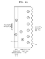
- FIG. 1 is a cross-sectional view of a photoelectric device according to an embodiment of the present disclosure.
- FIGS. 2A and 2B are cross-sectional views for explaining wet etching of a first semiconductor stack, respectively illustrating shapes before and after wet etching.
- FIGS. 3A and 3B are images illustrating an undercut of a gap insulation layer.
- FIGS. 4A and 4B are views for explaining wet etching of a first conductive semiconductor layer, schematically illustrating a distribution of electrons in a semiconductor substrate where the first conductive semiconductor layer is formed.
- FIGS. 5A and 5B are energy band diagrams at an interface between the first conductive semiconductor layer and the semiconductor substrate.
- FIG. 6 illustrates a mixture rate of an HNA etching solution.
- FIGS. 7A through 7O are cross-sectional views illustrating a method of manufacturing a photoelectric device, according to an embodiment of the present disclosure.
- FIG. 1 is a cross-sectional view of a photoelectric device according to an embodiment of the present disclosure.
- the photoelectric device includes a semiconductor substrate 100 , a first semiconductor stack 110 of a first conductive type and a second semiconductor stack 120 of a second conductive type that are formed on the semiconductor substrate 100 , and first and second electrodes 131 and 132 , respectively.
- the first and second electrodes 131 and 132 are also electrically connected to the first and second semiconductor stacks 110 and 120 , respectively.
- the first and second semiconductor stacks 110 and 120 may be alternately arranged on the semiconductor substrate 100 in plural.
- the semiconductor substrate 100 may include a first surface S 1 and a second surface S 2 opposite to the first surface S 1 .
- the second surface S 2 with no electrode structure functions as a light-receiving surface, effective incident light may be increased and light loss may be reduced.
- by forming a back-contact in which no electrode is formed on a light-receiving surface of the semiconductor substrate 100 light loss due to electrode surface area may be reduced. Also, compared with a conventional solar cell, a higher output may be obtained.
- the semiconductor substrate 100 may generate photogenerated carriers by receiving light through the second surface S 2 .
- the photogenerated carriers (hereinafter, referred to as carriers) signify holes and electrons generated by being absorbed in the semiconductor substrate 100 .
- the semiconductor substrate 100 may be formed as a monocrystal silicon substrate or polycrystal silicon substrate having n-type or p-type conductivity.
- the semiconductor substrate 100 may be formed as an n-type monocrystal silicon substrate.
- a texture structure T including an uneven pattern may be formed on the second surface S 2 of the semiconductor substrate 100 .
- the texture structure T may reduce reflectance of incident light and form an uneven surface including a plurality of fine protrusions.
- the texture structure T may include a wave shape, an uneven pattern shape, a gentle curve shape, a scalloped shape or a jagged shape.
- a capping layer 150 may be formed on the second surface S 2 of the semiconductor substrate 100 .
- the capping layer 150 may entirely cover the second surface S 2 of the semiconductor substrate 100 and may reduce etching reaction at the second surface S 2 and activate etching reaction at the first surface S 1 . Accordingly, of the first surface S 1 of the semiconductor substrate 100 , the first semiconductor stack 110 may be selectively patterned in a first semiconductor area A 1 and the second semiconductor stack 120 may be selectively patterned in a second semiconductor area A 2 , which is described below in detail.
- the capping layer 150 may be formed of an insulation material, for example, may include an insulation material having a band gap between a conduction band and a valence band that is equal to or more than 3.0 eV, to thus form an electric potential barrier on the second surface S 2 of the semiconductor substrate 100 .
- the capping layer 150 may include a silicon oxide (SiOx) layer or a silicon nitride (SiNx) layer.
- the capping layer 150 may be formed of a material having a work function of 5.0 eV or less.
- the capping layer 150 may be formed in the form of a single layer or a combined layer of two or more layers.
- the capping layer 150 may be formed in the form of a single layer of silicon oxide or silicon nitride, or a combined layer of silicon oxide and silicon nitride.
- the capping layer 150 may also have a passivation function of the second surface S 2 of the semiconductor substrate 100 . That is, the capping layer 150 prevents surface recombination of the carriers generated in the semiconductor substrate 100 to improve carrier collection efficiency. For example, the capping layer 150 may reduce recombination loss according to a surface defect of the semiconductor substrate 100 and improve carrier collection efficiency. Also, the capping layer 150 may be formed on the second surface S 2 that is a light-receiving surface of the semiconductor substrate 100 and may additionally have an antireflection function to reduce light reflectance and improve a light absorption rate. The capping layer 150 may include an uneven unpatterned surface shape, a wave shape, an uneven pattern shape, a gentle curve shape, a scalloped shape or a jagged shape.
- an etching barrier is formed at the second surface S 2 of the semiconductor substrate 100 and simultaneously passivation and antireflection effects of the second surface S 2 may be obtained.
- the capping layer 150 may be formed in the form of a combined layer of a first layer (not shown) with a passivation function and a second layer (not shown) with an antireflection function, in addition to the forming of an etching barrier at the second surface S 2 of the semiconductor substrate 100 .
- a passivation layer (not shown) and/or an antireflection layer (not shown) may be additionally formed on the capping layer 150 of the semiconductor substrate 100 , as a separate layer structure.
- the first and second semiconductor stacks 110 and 120 having opposite conductive types may be formed on the first surface S 1 of the semiconductor substrate 100 .
- the first and second semiconductor stacks 110 and 120 may be alternately arranged on the first surface S 1 of the semiconductor substrate 100 .
- the first and second semiconductor stacks 110 and 120 may respectively form an emitter and a base for separating and collecting the carriers generated in the semiconductor substrate 100 .
- the first and second semiconductor stacks 110 and 120 may be selectively formed in the first and second semiconductor areas A 1 and A 2 of the first surface S 1 of the semiconductor substrate 100 , respectively.
- the first semiconductor stack 110 may include a first intrinsic semiconductor layer 111 and a first conductive semiconductor layer 113 sequentially deposited in this order on the semiconductor substrate 100 .
- the first intrinsic semiconductor layer 111 and the first conductive semiconductor layer 113 may be formed of amorphous silicon (a-Si) or microcrystal silicon ( ⁇ c-Si).
- the first intrinsic semiconductor layer 111 may be formed by adding no dopant or adding a small amount of dopant.
- the first intrinsic semiconductor layer 111 may passivate the semiconductor substrate 100 to prevent recombination of the carriers generated in the semiconductor substrate 100 , and thus, an interface characteristic between the semiconductor substrate 100 of crystal silicon and the first conductive semiconductor layer 113 of a-Si may be improved.
- the first conductive semiconductor layer 113 may be formed by adding a p-type or n-type dopant.
- the first conductive semiconductor layer 113 may be doped with a p-type dopant to be opposite type to the semiconductor substrate 100 that is of an n-type and may form an emitter for collecting minority carriers, for example, holes, from the n-type semiconductor substrate 100 .
- the first semiconductor stack 110 may further include a first transparent conductive layer 115 formed on the first conductive semiconductor layer 113 .
- the first transparent conductive layer 115 may be electrically conductive and may include an optically transparent material.
- the first transparent conductive layer 115 may be formed of transparent conducting oxide (TCO) such as indium tin oxide (ITO), zinc oxide (ZnO), or the like.
- TCO transparent conducting oxide
- ITO indium tin oxide
- ZnO zinc oxide
- the first transparent conductive layer 115 interfaces or includes an electrical connection between the first conductive semiconductor layer 113 and the first electrode 131 and may reduce contact resistance therebetween.
- the second semiconductor stack 120 may include a second intrinsic semiconductor layer 121 and a second conductive semiconductor layer 123 sequentially deposited in this order on the semiconductor substrate 100 .
- the second intrinsic semiconductor layer 121 and the second conductive semiconductor layer 123 may be formed of a-Si or ⁇ c-Si, respectively.
- the second intrinsic semiconductor layer 121 may be formed without adding dopant or merely adding a relatively small amount of dopant.
- the second intrinsic semiconductor layer 121 may passivate a surface of the semiconductor substrate 100 to prevent recombination of the carriers generated in the semiconductor substrate 100 , and thus, an interface characteristic between the semiconductor substrate 100 of crystal silicon and the second conductive semiconductor layer 123 of a-Si may be improved.
- the second conductive semiconductor layer 123 may be formed by adding an n-type or p-type dopant.
- the second conductive semiconductor layer 123 may be doped with an n-type dopant like the semiconductor substrate 100 that is of an n-type and may form a base for collecting majority carriers, for example, electrons, from the n-type semiconductor substrate 100 .
- the second semiconductor stack 120 may further include a second transparent conductive layer 125 formed on the second conductive semiconductor layer 123 .
- the second transparent conductive layer 125 may be electrically conductive and may include an optically transparent material.
- the second transparent conductive layer 125 may be formed of TCO such as ITO, ZnO, or the like.
- the second transparent conductive layer 125 interfaces or includes an electrical connection between the second conductive semiconductor layer 123 and the second electrode 132 and may reduce contact resistance therebetween.
- the first and second semiconductor stacks 110 and 120 form an emitter and a base respectively including the first and second intrinsic semiconductor layers 111 and 121 and the first and second conductive semiconductor layers 113 and 123 .
- the first and second semiconductor stacks 110 and 120 may respectively include the first and second conductive semiconductor layers 113 and the 123 only, without the first and second intrinsic semiconductor layers 111 and 121 .
- the first and second semiconductor stacks 110 and 120 respectively include the first and second transparent conductive layers 115 and 125 interfacing or including the electrical connection between the first and second electrodes 131 and 132 .
- the first and second transparent conductive layers 115 and 125 are not formed.
- the first and second electrodes 131 and 132 may be formed directly on the first and second semiconductor stacks 110 and 120 without the first and second transparent conductive layers 115 and 125 therebetween.
- the first and second electrodes 131 and 132 may be formed on the first and second semiconductor stacks 110 and 120 , respectively.
- the first and second electrodes 131 and 132 may be electrically connected to the first and second semiconductor stacks 110 and 120 , respectively, and be configured to draw the photogenerated carriers to the outside.
- the first and second electrodes 131 and 132 may include a metal material such as silver (Ag), aluminum (Al), copper (Cu), nickel (Ni), and the like.
- the first and second electrodes 131 and 132 form a current path for a photocurrent and may be formed of a metal material exhibiting superior electric conductivity to reduce a serial resistance.
- FIG. 1 the shapes of the first and second electrodes 131 and 132 are illustrated in a widthwise direction. In contrast, the first and second electrodes 131 and 132 may be formed in strips in a current draw direction.
- a gap insulation layer 160 may be formed between the first and second semiconductor stacks 110 and 120 .
- the gap insulation layer 160 may cover a portion between the first and second semiconductor stacks 110 and 120 , may passivate a surface of the semiconductor substrate 100 exposed between the first and second semiconductor stacks 110 and 120 , and may be formed to secure insulation between the first and second semiconductor stacks 110 and 120 .
- end portions of the first and second semiconductor stacks 110 and 120 may be formed to cover part of the gap insulation layer 160 .
- the gap insulation layer 160 may be formed of an oxide layer (SiOx) or a nitride layer (SiNx).
- the first and second semiconductor stacks 110 and 120 are respectively formed in the first and second semiconductor areas A 1 and A 2 of the semiconductor substrate 100 .
- the first semiconductor stack 110 may be selectively formed in the first semiconductor area A 1
- the second semiconductor stack 120 may be selectively formed in the second semiconductor area A 2 .
- the first semiconductor stack 110 may be formed by patterning a material layer formed over the entire first surface S 1 of the semiconductor substrate 100 . For example, among the material layer of the first intrinsic semiconductor layer 111 , the first conductive semiconductor layer 113 , and the first transparent conductive layer 115 formed on the semiconductor substrate 100 , the first semiconductor stack 110 locally formed in the first semiconductor area A 1 may be obtained by selectively etching away the material layer in the other area than the first semiconductor area A 1 .
- Wet etching may be used when patterning to form first semiconductor stack 110 .
- a mixed solution of Hydrofluoric acid+Nitric Acid+Acetic acid (HNA) of nitric acid (HNO 3 ), hydrofluoric acid (HF), and acetic acid (CH 3 COOH), or nitric acid (HNO 3 ), hydrofluoric acid (HF), and pure water (DI water) may be used as an etchant.
- HNA Hydrofluoric acid+Nitric Acid+Acetic acid
- HNO 3 nitric acid
- HF hydrofluoric acid
- DI water pure water
- wet etching is advantageous for mass production and has a relatively low manufacturing cost.
- mass productivity of a photoelectric device may be improved and manufacturing costs may be reduced.
- reactive ion etching which is a type of dry etching, requires expensive special equipment and a high-energy ion bombardment is incurred, thereby increasing overall manufacturing costs.
- FIGS. 2A and 2B are cross-sectional views for illustrating wet etching of the first semiconductor stack 110 , respectively illustrating shapes before and after wet etching.
- the first intrinsic semiconductor layer 111 , the first conductive semiconductor layer 113 , and the first transparent conductive layer 115 are formed over the entire first surface S 1 of the semiconductor substrate 100 , that is, the entire first surface S 1 including the gap insulation layer 160 , thereby forming a first semiconductor stack material layer 110 ′.
- the first semiconductor stack material layer 110 ′ in the other area than the first semiconductor area A 1 is removed by using an etch mask M 1 to form the first semiconductor stack 110 .
- the gap insulation layer 160 has a bottom surface 161 contacting the semiconductor substrate 100 and left and right side surfaces 162 and 163 connected to the bottom surface 161 .
- the undercut R may be formed in any one of the left and right side surfaces 162 and 163 , that is, a side surface exposed by the etch mask M 1 , for example, the right side surface 163 .
- FIGS. 3A and 3B are images illustrating the undercut of the gap insulation layer 160 .
- FIG. 3A illustrates an area where the gap insulation layer 160 is formed (Gap area), an area where the etch mask M 1 is formed (ER area), and an area where the gap insulation layer 160 and the etch mask M 1 overlap (ER overlap).
- FIG. 3B illustrates that the undercut is formed in the gap insulation layer 160 (SiNx).
- the undercut may be uniquely formed via wet etching.
- wet etching a kind of dry etching, ion bombardment with directivity is used and thus no undercut occurs in the side surface of the gap insulation layer 160 .
- the capping layer 150 is formed on the second surface S 2 of the semiconductor substrate 100 before the wet etching of the first semiconductor stack material layer 110 ′.
- the capping layer 150 is formed on the second surface S 2 that is opposite to the first surface S 1 where the first semiconductor stack material layer 110 ′ is formed.
- the capping layer 150 may thus be configured to prevent a reaction between an etching solution and the second surface S 2 of the semiconductor substrate 100 and may prevent leakage of electrons through the second surface S 2 by forming an electric potential barrier on the second surface S 2 . Accordingly, a sufficient number of electrons that participate in the etching reaction of the first semiconductor stack material layer 110 ′ may be secured, and thus, etching may be activated.
- an acid solution for example, HNA
- HNA acid solution
- the first conductive semiconductor layer 113 doped to have p-type conductivity has a relatively low etching rate due to the lack of electrons that participate in the etching reaction, which is a hindrance factor that restricts the etching of the first semiconductor stack 110 .
- the following description focuses on the first semiconductor stack 110 , particularly, the etching of the first conductive semiconductor layer 113 .
- HNA provides NO 2 that is a strong oxidizing agent of silicon, and the NO 2 receives electrons from a surface of silicon to oxidize the silicon.
- the oxidized silicon reacts with a hydroxyl group (OH ⁇ ) to produce a soluble material and is removed by being dissolved.
- the series of reactions may be summarized as follows: 2NO 2 +Si ⁇ 2NO 2 ⁇ +Si 2 + (1) Si 2 ++2OH ⁇ SiO 2 +H 2 (2) SiO 2 +6HF ⁇ H 2 SiF 6 (Soluble)+H 2 O (3)
- the series of etching processes may be performed on the first conductive semiconductor layer 113 exposed to the etching solution or the second surface S 2 of the semiconductor substrate 100 opposite to the first conductive semiconductor layer 113 .
- the silicon in the reactions (1) and (2) may correspond to the silicon of the first conductive semiconductor layer 113 or the silicon of the semiconductor substrate 100 .
- FIGS. 4A and 4B are views illustrating wet etching of the first conductive semiconductor layer 113 , and schematically illustrating a distribution of electrons in the semiconductor substrate 100 where the first conductive semiconductor layer 113 is formed.
- FIGS. 4A and 4B illustrate distributions of electrons before and after the forming of the capping layer 150 , respectively.
- “ ⁇ circle around (e) ⁇ ” indicates an electron.
- the second surface S 2 of the semiconductor substrate 100 shows a relatively high electron density
- the first surface S 1 of the semiconductor substrate 100 that is, the first conductive semiconductor layer 113
- This distribution of electrons shows that electrons move toward the semiconductor substrate 100 , that is, the second surface S 2 of the semiconductor substrate 100 , according to an electric field of a p-n junction between the n-type doped semiconductor substrate 100 and the p-type doped first conductive semiconductor layer 113 .
- FIGS. 5A and 5B are energy band diagrams at an interface between the first conductive semiconductor layer 113 and the semiconductor substrate 100 .
- FIGS. 5A and 5B illustrate energy band diagrams before and after the forming of the capping layer 150 , respectively.
- “ ⁇ circle around (e) ⁇ ” and “ ⁇ circle around (h) ⁇ ”, respectively, indicate an electron and a hole.
- Ec, Ef, and Ev respectively denote a conduction band, a Fermi level, and a valence band.
- an internal electric field is formed between the n-type doped semiconductor substrate 100 and the p-type doped first conductive semiconductor layer 113 according to a p-n junction. Electrons move toward the semiconductor substrate 100 , that is, the second surface S 2 of the semiconductor substrate 100 , along the internal electric field and react with the etching solution, thereby etching the second surface S 2 of the semiconductor substrate 100 . In other words, not the first conductive semiconductor layer 113 that is subject to etching, but the second surface S 2 of the semiconductor substrate 100 is etched away.
- the first surface S 1 of the semiconductor substrate 100 lacks electrons that participate in the reaction, and thus, etching of the first conductive semiconductor layer 113 is delayed. Furthermore, as an etching reaction is actively performed on the second surface S 2 of the semiconductor substrate 100 , an etching rate decreases at the first surface S 1 of the semiconductor substrate 100 due to a Galvanic effect, and thus, etching is further delayed.
- FIG. 5B schematically illustrates a distribution of electrons when the capping layer 150 is formed on the second surface S 2 of the semiconductor substrate 100 .
- FIG. 5B schematically illustrates a distribution of electrons when the capping layer 150 is formed on the second surface S 2 of the semiconductor substrate 100 .
- leakage of electrons through the second surface S 2 of the semiconductor substrate 100 may be prevented.
- a sufficient amount of electrons participate in the reaction in the first surface S 1 of the semiconductor substrate 100 ; that is, the etching of the first conductive semiconductor layer 113 , may be secured.
- FIG. 5A and FIG. 5B are compared with each other, it can be seen that a greater number of electrons exist in the first conductive semiconductor layer 113 due to the coating of the capping layer 150 .
- FIG. 5B is an energy band diagram when the capping layer 150 is formed on the second surface S 2 of the semiconductor substrate 100 .
- an internal electric field is formed between the n-type doped semiconductor substrate 100 and the p-type doped first conductive semiconductor layer 113 according to a p-n junction.
- the capping layer 150 forms an electric potential barrier on the second surface S 2 of the semiconductor substrate 100 , the reaction between the electrons and the etching solution may be prevented. Accordingly, the leakage of electrons through the second surface S 2 of the semiconductor substrate 100 is prevented and thus a sufficient amount of electrons for the etching of the first conductive semiconductor layer 113 may be secured.
- the capping layer 150 may include an insulator having a large band gap between a conduction band (Ec) and a valence band (Ev) to form an electric potential barrier on the second surface S 2 of the semiconductor substrate 100 .
- the capping layer 150 may include an insulator having a band gap of 3.0 eV or more.
- the capping layer 150 may include a material having a small work function, for example, a material having a work function of 5.0 eV or less.
- the capping layer 150 may include a silicon oxide (SiO x ) layer or a silicon nitride (SiN x ) layer.
- the capping layer 150 may be formed in the form of a single layer or a combined layer of two or more layers.
- FIG. 6 illustrates a mixture rate of an HNA etching solution.
- three sides forming a triangle indicate mixture rates of three components of an HF solution, an HNO 3 solution, and H 2 O (DI water).
- the HF solution is diluted at 49 wt % and the HNO 3 solution is diluted at 63 wt %.
- the HF solution, the HNO 3 solution, and H 2 O indicate a mixture rate of about 0 wt % to about 100 wt % along each side in units of weight percentages.
- Etching solutions ⁇ circle around (1) ⁇ to ⁇ circle around (9) ⁇ with different mixture rates are shown on the triangle.
- Table 1 shows detailed mixture rates of the etching solutions ⁇ circle around (1) ⁇ to ⁇ circle around (9) ⁇ and whether etching is performed.
- Whether etching is performed is determined according to whether a porous surface is formed in the first conductive semiconductor layer 113 that is exposed to the etching solution for a predetermined time or not.
- etching solutions ⁇ circle around (7) ⁇ , ⁇ circle around (8) ⁇ , and ⁇ circle around (9) ⁇ since a porous surface is formed in the first conductive semiconductor layer 113 exposed to the etching solution for about 2 hours, it is determined that etching has been performed.
- etching solutions ⁇ circle around (1) ⁇ to ⁇ circle around (6) ⁇ since a porous surface is not observed after exposure for three hours, it is determined that etching has not been performed.
- HNA solutions in Table 1 etching seems to be smoothly performed when a mixture rate of HNO 3 is high and a mixture rate of H 2 O is low.
- etching can be performed when the mixture rate of HNO 3 is 75 wt % or more, in particular, 77 wt % or more, and when the mixture rate of H 2 O (DI water) is 15 wt % or less, in particular, 10 wt % or less.
- the mixture rate of H 2 O means a mixture rate with the HF solution and the HNO 3 solution. Since the HF solution and the HNO 3 solution are respectively diluted at 49 wt % and 63 wt %, a total mixture rate of H 2 O indicates a total mixture rate of H 2 O considering the dilution rates of the HF solution and the HNO 3 solution, that is, a total mixture rate of H 2 O considering H 2 O that forms 51 wt % of the HF solution and 37 wt % of the HNO 3 solution. In terms of the total mixture rate of H 2 O, etching may be performed at 50 wt % or less.
- FIGS. 7A through 7O are cross-sectional views illustrating a method of manufacturing a photoelectric device, according to an embodiment of the present disclosure.
- a semiconductor substrate 200 is prepared.
- the semiconductor substrate 200 may be an n-type crystal silicon wafer.
- a washing process using an acidic or alkaline solution may be performed to remove physical or chemical impurities adhering on a surface of the semiconductor substrate 200 .
- an insulation layer 260 ′ is formed on a first surface S 1 of the semiconductor substrate 200 .
- the insulation layer 260 ′ functions as an etch mask during texturing to form an uneven pattern on a second surface S 2 of the semiconductor substrate 200 and may be formed of a material having tolerance to a texturing etchant. Also, a remaining part of the insulation layer 260 ′ may form a gap insulation layer 260 through a patterning process that is described below.
- the insulation layer 260 ′ may be formed as a silicon oxide (SiO x ) layer or a silicon nitride (SiN x ) layer, or as a combined layer of an oxide layer and a nitride layer.
- the insulation layer 260 ′ may be formed by growing an oxide layer by a thermal oxidation method or by depositing an oxide layer or a nitride layer by a chemical vapor deposition (CVD) method.
- texturing may be performed on the second surface S 2 of the semiconductor substrate 200 .
- the second surface S 2 of the semiconductor substrate 200 is etched by using the insulation layer 260 ′ formed on the first surface S 1 of the semiconductor substrate 200 as an etch mask.
- a texture structure T with an uneven pattern may be formed on the second surface S 2 of the semiconductor substrate 200 .
- the texture structure T according to the disclosure of the present application may include a number of different pattern or unpatterned shaped surfaces.
- a capping layer 250 may be formed on the second surface S 2 of the semiconductor substrate 200 .
- the capping layer 250 prevents a reaction between the etching solution and the second surface S 2 of the semiconductor substrate 200 and activates etching of a first semiconductor stack 210 formed on the first surface S 1 of the semiconductor substrate 200 in wet etching that is described below.
- the capping layer 250 may be formed of an insulator having a large band gap between a conduction band and a valence band, to form an electric potential barrier on the second surface S 2 of the semiconductor substrate 200 .
- the capping layer 250 may include a silicon oxide (SiO x ) layer or a silicon nitride (SiN x ) layer.
- the capping layer 250 may be formed in the form of a single layer of silicon oxide or silicon nitride, or a combined layer of two or more layers including a silicon oxide layer and a silicon nitride layer together.
- the capping layer 250 may thus be configured to perform a passivation function to reduce surface recombination loss of the carriers generated in the semiconductor substrate 200 by covering the second surface S 2 of the semiconductor substrate 200 . Also, the capping layer 250 may be configured to perform an antireflection function to reduce reflectance of incident light and absorb the incident light in the semiconductor substrate 200 as much as possible. For example, by forming the capping layer 250 in form of a silicon oxide (SiO x ) layer, a silicon nitride (SiN x ) layer, or a hydrogenated silicon nitride layer (SiN:H), the wet etching on the rear surface of the capping layer 250 is facilitated and simultaneously passivation and antireflection effects may be achieved. In another embodiment, the capping layer 250 may be formed as a first layer (not shown) with an additional passivation function and a second layer (not shown) with an additional antireflection function.
- SiO x silicon oxide
- SiN x silicon nitride
- the capping layer 250 may be formed as a separate layer from the passivation layer and/or the antireflection layer.
- the passivation layer may be formed on the second surface S 2 of the semiconductor substrate 200 and the capping layer may be formed on the passivation layer as a separate layer.
- the passivation layer may be formed of intrinsic a-Si or doped a-Si.
- the passivation layer may be formed to have the same conductive type as the semiconductor substrate 200 , thereby forming a front surface field (FSF).
- FSF front surface field
- the capping layer 250 may be formed on the passivation layer.
- the gap insulation layer 260 is formed by patterning the insulation layer 260 ′ on the first surface S 1 of the semiconductor substrate 200 .
- an etch mask M 6 is formed in a partial area of the insulation layer 260 ′, and a part of the insulation layer 260 ′ not covered by the etch mask M 6 is etched and removed.
- An acidic solution such as HF or H 3 PO 4 having an etching characteristic to the insulation layer 260 ′ may be used as an etchant.
- the etch mask M 6 is removed.
- a first intrinsic semiconductor layer 211 may be formed on the first surface S 1 of the semiconductor substrate 200 .
- the first intrinsic semiconductor layer 211 may be formed over the entire first surface S 1 of the semiconductor substrate 200 to also be formed over the gap insulation layer 260 .
- the first intrinsic semiconductor layer 211 may be formed by a CVD method using silane (SiH 4 ) that is a silicon containing gas, or may be formed of a-Si.
- a first conductive semiconductor layer 213 is formed on the first intrinsic semiconductor layer 211 .
- the first conductive semiconductor layer 213 may be doped to have p-type conductivity that is opposite to that of the semiconductor substrate 200 .
- the first conductive semiconductor layer 213 may be formed by a CVD method using a doping gas, for example, B 2 H 6 , with SiH 4 as a source.
- a first transparent conductive layer 215 is formed on the first conductive semiconductor layer 213 .
- the first transparent conductive layer 215 may be formed of TCO such as ITO, ZnO, and the like by a sputtering or CVD method.
- the first intrinsic semiconductor layer 211 , the first conductive semiconductor layer 213 , and the first transparent conductive layer 215 are sequentially formed in this order on the first surface S 1 of the semiconductor substrate 200 , thereby forming a first semiconductor stack material layer 210 ′.
- the first semiconductor stack material layer 210 ′ is patterned by wet etching so that the first semiconductor stack 210 that is selectively formed in the first semiconductor area A 1 may be obtained.
- an etch stop layer 218 may be additionally formed on the first transparent conductive layer 215 .
- the etch stop layer 218 does not form the first semiconductor stack 210 , but instead, may be configured to prevent etching of the first semiconductor stack 210 during patterning of a second semiconductor stack.
- the etch stop layer 218 may be employed for convenience of manufacturing and may be removed before the final step of a manufacturing process.
- the etch stop layer 218 may be formed as a titanium-tungsten (TiW) layer by a sputtering method.
- the first semiconductor stack 210 may be formed by patterning the first semiconductor stack material layer 210 ′ and the etch stop layer 218 , which are formed on the first surface S 1 of the semiconductor substrate 200 .
- the first semiconductor stack 210 may be selectively formed in the first semiconductor area A 1 and in the first semiconductor area A 1 including part of the gap insulation layer 260 .
- the first semiconductor stack material layer 210 ′ and the etch stop layer 218 which are formed in the second semiconductor area A 2 and in the center portion of the gap insulation layer 260 may be etched and removed.
- wet etching may be used for patterning the first semiconductor stack 210 .
- the etch mask M 1 is employed in the first semiconductor area A 1 to remove a portion exposed around the etch mask M 1 .
- An acid etching solution such as HNA may be employed as an etchant.
- the capping layer 250 formed on the second surface S 2 of the semiconductor substrate 200 may activate etching of the first semiconductor stack material layer 210 ′ on the first surface S 1 , in particular, the first conductive semiconductor layer 213 .
- the capping layer 250 may be configured to restrict the reaction between the second surface S 2 and the etching solution and may be configured to form an electric potential barrier on the second surface S 2 so that the etching reaction of the first conductive semiconductor layer 213 on the first surface S 1 may be activated may be activated.
- the first semiconductor stack 210 and the etch stop layer 218 are formed, and are patterned to cover the first semiconductor area A 1 , and the etch mask M 1 may be removed.
- the layers may be sequentially patterned in a deposition direction, for example, by patterning the etch stop layer 218 using an etching solution including hydrogen peroxide (H 2 O 2 ), patterning the first transparent conductive layer 215 using an acid etching solution such as HCl, HNO 3 , etc, and patterning the first conductive semiconductor layer 213 and the first intrinsic semiconductor layer 211 .
- H 2 O 2 hydrogen peroxide
- the layers may be sequentially patterned in a deposition direction, for example, by patterning the etch stop layer 218 using an etching solution including hydrogen peroxide (H 2 O 2 ), patterning the first transparent conductive layer 215 using an acid etching solution such as HCl, HNO 3 , etc, and patterning the first conductive semiconductor layer 213 and the first intrinsic semiconductor layer 211 .
- a second intrinsic semiconductor layer 221 may be formed on the first surface S 1 of the semiconductor substrate 200 .
- the second intrinsic semiconductor layer 221 may be formed over the entire surface of the semiconductor substrate 200 including the first semiconductor stack 210 .
- the second intrinsic semiconductor layer 221 may be formed by a CVD method using SiH 4 that is a silicon containing gas, or may be formed of a-Si.
- a second conductive semiconductor layer 223 is formed on the second intrinsic semiconductor layer 221 .
- the second conductive semiconductor layer 223 may be formed to have an n-type conductivity that is the same type as that of the semiconductor substrate 200 and may be formed by a CVD method using a doping gas, for example, PH 3 , with SiH 4 as a source, or may be formed of a-Si.
- a second transparent conductive layer 225 is formed on the second conductive semiconductor layer 223 .
- the second transparent conductive layer 225 may be formed of TCO such as ITO, ZnO, and the like. by a sputtering or CVD method.
- the second intrinsic semiconductor layer 221 , the second conductive semiconductor layer 223 , and the second transparent conductive layer 225 are sequentially formed in this order on the semiconductor substrate 200 , thereby forming a second semiconductor stack material layer 220 ′.
- the second semiconductor stack material layer 220 ′ is wet-etched and patterned so that a second semiconductor stack 220 selectively formed in the second semiconductor area A 2 is obtained, which is described in further detail below.
- the second semiconductor stack 220 may be formed by patterning the second semiconductor stack material layer 220 ′ formed on the first surface S 1 of the semiconductor substrate 200 .
- the second semiconductor stack 220 may be selectively formed in the second semiconductor area A 2 and in the second semiconductor area A 2 including part of the gap insulation layer 260 .
- the second semiconductor stack material layer 220 ′ formed in the first semiconductor area A 1 and in the center portion of the gap insulation layer 260 may be etched and removed.
- wet etching may be used for patterning the second semiconductor stack material layer 220 ′.
- an etch mask M 2 is employed in the second semiconductor area A 2 to remove a portion exposed around the etch mask M 2 .
- An acid etching solution such as HNA may be employed as an etchant.
- the etch stop layer 218 is formed on the first semiconductor stack 210 , the first semiconductor stack 210 may be protected to not be etched.
- the capping layer 250 formed on the second surface S 2 of the semiconductor substrate 200 may activate etching of the second semiconductor stack material layer 220 ′ at the first surface S 1 .
- the capping layer 250 restricts the reaction between the second surface S 2 and the etching solution and forms an electric potential barrier on the second surface S 2 so that the etching reaction of the second semiconductor stack material layer 220 ′ may be activated.
- the activation of etching by the capping layer 250 may be effectively achieved in the wet etching of the first conductive semiconductor layer 213 or the second conductive semiconductor layer 223 that is doped to have p-type conductivity. Also, the activation effect may be obtained in the wet etching of the other first conductive semiconductor layer 213 or second conductive semiconductor layer 223 that is doped to have n-type conductivity. This is because the capping layer 250 may be configured to restrict the reaction between the second surface S 2 and the etching solution and forms an electric potential barrier on the second surface S 2 so that the etching of the first conductive semiconductor layer 213 or the second conductive semiconductor layer 221 on the first surface S 1 may be activated as described above with reference to FIGS. 4B and 5B .
- layers from the second intrinsic semiconductor layer 221 to the second transparent conductive layer 225 formed on the semiconductor substrate 200 are illustrated to be patterned simultaneously; the present disclosure is not limited thereto.
- the layers may be sequentially patterned in a deposition direction, for example, by patterning the second transparent conductive layer 225 using an acid etching solution such as HCl, HNO 3 , etc, and then patterning the second conductive semiconductor layer 223 and the second intrinsic semiconductor layer 221 .
- the second semiconductor stack 220 is formed as a pattern that covers the second semiconductor area A 2 .
- the first and second semiconductor stacks 210 and 220 may be alternately arranged on the first surface S 1 of the semiconductor substrate 200 in plural.
- the etch stop layer 218 formed on the first semiconductor stack 210 is removed.
- the etch stop layer 218 may be removed by using an etching solution including hydrogen peroxide (H 2 O 2 ) and the other portions than the etch stop layer 218 may be protected by an etch mask (not shown).
- H 2 O 2 hydrogen peroxide
- first and second electrodes 231 and 232 are formed on the first and second semiconductor stacks 210 and 220 , respectively.
- the first and second electrodes 231 and 232 are electrically connected to the second semiconductor stacks 210 and 220 , respectively, and thus carriers may be drawn to the outside.
- the first and second electrodes 231 and 232 may include a metal material such as silver (Ag), aluminum (Al), copper (Cu), nickel (Ni), and the like.
- metal paste is pattern printed by employing screen printing and then the first and second electrodes 231 and 232 may be formed through thermal plasticity.
- an etching reaction may be activated during wet etching. Also, since a photoelectric device is manufactured by employing wet etching advantageous to mass production, mass productivity of a photoelectric device may be improved and manufacturing cost may be reduced.
Landscapes
- Photovoltaic Devices (AREA)
- Engineering & Computer Science (AREA)
- Manufacturing & Machinery (AREA)
Abstract
Description
2NO2+Si→2NO2−+Si2+ (1)
Si2++2OH−→SiO2+H2 (2)
SiO2+6HF→H2SiF6(Soluble)+H2O (3)
| TABLE 1 | |||||
| Etching | |||||
| Total H2O | performed | ||||
| HF (%) | HNO3 (%) | H2O (%) | (%) | (hours) | |
| {circle around (1)} | 2 | 82 | 16 | 47.4 | X (3) |
| {circle around (2)} | 2 | 16 | 82 | 88.9 | X (3) |
| {circle around (3)} | 3 | 73 | 24 | 52.5 | X (3) |
| {circle around (4)} | 14 | 14 | 72 | 83.3 | X (3) |
| {circle around (5)} | 3 | 16 | 81 | 88.5 | X (3) |
| {circle around (6)} | 11 | 33 | 56 | 73.8 | X (3) |
| {circle around (7)} | 9 | 91 | 0 | 38.3 | ◯ (2) |
| {circle around (8)} | 8 | 84 | 8 | 43.2 | ◯ (2) |
| {circle around (9)} | 8 | 77 | 15 | 47.6 | ◯ (2) |
Claims (14)
Applications Claiming Priority (2)
| Application Number | Priority Date | Filing Date | Title |
|---|---|---|---|
| KR1020120075741A KR101977927B1 (en) | 2012-07-11 | 2012-07-11 | Photoelectric device and the manufacturing method thereof |
| KR10-2012-0075741 | 2012-07-11 |
Publications (2)
| Publication Number | Publication Date |
|---|---|
| US20140015087A1 US20140015087A1 (en) | 2014-01-16 |
| US8852982B2 true US8852982B2 (en) | 2014-10-07 |
Family
ID=49913280
Family Applications (1)
| Application Number | Title | Priority Date | Filing Date |
|---|---|---|---|
| US13/838,643 Active US8852982B2 (en) | 2012-07-11 | 2013-03-15 | Photoelectric device and manufacturing method thereof |
Country Status (2)
| Country | Link |
|---|---|
| US (1) | US8852982B2 (en) |
| KR (1) | KR101977927B1 (en) |
Families Citing this family (1)
| Publication number | Priority date | Publication date | Assignee | Title |
|---|---|---|---|---|
| EP3163632A1 (en) * | 2015-11-02 | 2017-05-03 | CSEM Centre Suisse d'Electronique et de Microtechnique SA - Recherche et Développement | Photovoltaic device and method for manufacturing the same |
Citations (11)
| Publication number | Priority date | Publication date | Assignee | Title |
|---|---|---|---|---|
| KR100611753B1 (en) | 2004-05-03 | 2006-08-10 | 삼성에스디아이 주식회사 | Manufacturing Method of Thin Film Transistor |
| KR100623686B1 (en) | 2004-05-12 | 2006-09-19 | 삼성에스디아이 주식회사 | Manufacturing Method of Thin Film Transistor |
| US7339110B1 (en) | 2003-04-10 | 2008-03-04 | Sunpower Corporation | Solar cell and method of manufacture |
| KR20080105280A (en) | 2007-05-30 | 2008-12-04 | 엘지전자 주식회사 | Manufacturing method of solar cell and solar cell manufactured using same |
| US20090223562A1 (en) * | 2006-10-27 | 2009-09-10 | Kyocera Corporation | Solar Cell Element Manufacturing Method and Solar Cell Element |
| US20090283800A1 (en) | 2008-05-12 | 2009-11-19 | The Regents Of The University Of California | Photoelectrochemical etching of p-type semiconductor heterostructures |
| US20090305456A1 (en) | 2005-09-22 | 2009-12-10 | Yasushi Funakoshi | Method of Manufacturing Back Junction Solar Cell |
| JP2010016130A (en) | 2008-07-02 | 2010-01-21 | Ulvac Japan Ltd | Manufacturing method of porous film, the porous film, and solution of precursor composition of the porous film |
| US20100267187A1 (en) | 2007-12-13 | 2010-10-21 | Yasushi Funakoshi | Method for manufacturing solar cell |
| US20110303280A1 (en) * | 2010-06-14 | 2011-12-15 | Imec | Fabrication method for interdigitated back contact photovoltaic cells |
| US20120045866A1 (en) * | 2008-05-17 | 2012-02-23 | Astrowatt, Inc. | Method of forming an electronic device using a separation technique |
Family Cites Families (8)
| Publication number | Priority date | Publication date | Assignee | Title |
|---|---|---|---|---|
| FR2880989B1 (en) * | 2005-01-20 | 2007-03-09 | Commissariat Energie Atomique | SEMICONDUCTOR DEVICE WITH HETEROJUNCTIONS AND INTERDIGITAL STRUCTURE |
| JP4999937B2 (en) * | 2008-01-30 | 2012-08-15 | 京セラ株式会社 | Solar cell element and method for manufacturing solar cell element |
| US7851698B2 (en) * | 2008-06-12 | 2010-12-14 | Sunpower Corporation | Trench process and structure for backside contact solar cells with polysilicon doped regions |
| US8450141B2 (en) * | 2009-06-17 | 2013-05-28 | University Of Delaware | Processes for fabricating all-back-contact heterojunction photovoltaic cells |
| DE202010018510U1 (en) * | 2009-09-07 | 2017-03-15 | Lg Electronics Inc. | solar cell |
| JP5906393B2 (en) * | 2010-02-26 | 2016-04-20 | パナソニックIpマネジメント株式会社 | Solar cell and method for manufacturing solar cell |
| JP2011204832A (en) * | 2010-03-25 | 2011-10-13 | Sanyo Electric Co Ltd | Solar cell and method for manufacturing the same |
| US8633379B2 (en) * | 2010-08-17 | 2014-01-21 | Lg Electronics Inc. | Solar cell |
-
2012
- 2012-07-11 KR KR1020120075741A patent/KR101977927B1/en active Active
-
2013
- 2013-03-15 US US13/838,643 patent/US8852982B2/en active Active
Patent Citations (11)
| Publication number | Priority date | Publication date | Assignee | Title |
|---|---|---|---|---|
| US7339110B1 (en) | 2003-04-10 | 2008-03-04 | Sunpower Corporation | Solar cell and method of manufacture |
| KR100611753B1 (en) | 2004-05-03 | 2006-08-10 | 삼성에스디아이 주식회사 | Manufacturing Method of Thin Film Transistor |
| KR100623686B1 (en) | 2004-05-12 | 2006-09-19 | 삼성에스디아이 주식회사 | Manufacturing Method of Thin Film Transistor |
| US20090305456A1 (en) | 2005-09-22 | 2009-12-10 | Yasushi Funakoshi | Method of Manufacturing Back Junction Solar Cell |
| US20090223562A1 (en) * | 2006-10-27 | 2009-09-10 | Kyocera Corporation | Solar Cell Element Manufacturing Method and Solar Cell Element |
| KR20080105280A (en) | 2007-05-30 | 2008-12-04 | 엘지전자 주식회사 | Manufacturing method of solar cell and solar cell manufactured using same |
| US20100267187A1 (en) | 2007-12-13 | 2010-10-21 | Yasushi Funakoshi | Method for manufacturing solar cell |
| US20090283800A1 (en) | 2008-05-12 | 2009-11-19 | The Regents Of The University Of California | Photoelectrochemical etching of p-type semiconductor heterostructures |
| US20120045866A1 (en) * | 2008-05-17 | 2012-02-23 | Astrowatt, Inc. | Method of forming an electronic device using a separation technique |
| JP2010016130A (en) | 2008-07-02 | 2010-01-21 | Ulvac Japan Ltd | Manufacturing method of porous film, the porous film, and solution of precursor composition of the porous film |
| US20110303280A1 (en) * | 2010-06-14 | 2011-12-15 | Imec | Fabrication method for interdigitated back contact photovoltaic cells |
Non-Patent Citations (1)
| Title |
|---|
| B. Schwartz and H. Robbins, Chemical Etching of Silicon : IV. Etching Technology, Journal of the electochemical society, Dec. 1976, 1903-1909 pp., vol. 123, issue 12, The Electrochemical Society. |
Also Published As
| Publication number | Publication date |
|---|---|
| KR20140009615A (en) | 2014-01-23 |
| US20140015087A1 (en) | 2014-01-16 |
| KR101977927B1 (en) | 2019-05-13 |
Similar Documents
| Publication | Publication Date | Title |
|---|---|---|
| US8569614B2 (en) | Solar cell and method of manufacturing the same | |
| US10680122B2 (en) | Solar cell and method for manufacturing the same | |
| US7858426B2 (en) | Method of texturing solar cell and method of manufacturing solar cell | |
| US10084107B2 (en) | Transparent conducting oxide for photovoltaic devices | |
| EP2219222A2 (en) | Solar cell and method for manufacturing the same | |
| US20140099747A1 (en) | Semiconductor device and method for manufacturing the same | |
| US20100132792A1 (en) | Solar cell and method of manufacturing the same | |
| US20100218821A1 (en) | Solar cell and method for manufacturing the same | |
| KR20100118864A (en) | A fabricating method of buried contact solar cell | |
| EP2538447B1 (en) | Solar cell and method for manufacturing the same | |
| US20160268459A1 (en) | Photoelectric conversion element, photoelectric conversion module, and solar photovoltaic power generation system | |
| CN103515456A (en) | Solar cell | |
| KR20180018895A (en) | Bifacial silicon solar cell | |
| US9997647B2 (en) | Solar cells and manufacturing method thereof | |
| KR101612133B1 (en) | Metal Wrap Through type solar cell and method for fabricating the same | |
| KR101714779B1 (en) | Solar cell and manufacturing method thereof | |
| CN104810414B (en) | Solar cell and its manufacture method | |
| KR20130042435A (en) | Photoelectric device | |
| KR101198430B1 (en) | Bifacial Photovoltaic Localized Emitter Solar Cell and Method for Manufacturing Thereof | |
| JP5645734B2 (en) | Solar cell element | |
| KR101198438B1 (en) | Bifacial Photovoltaic Localized Emitter Solar Cell and Method for Manufacturing Thereof | |
| US8852982B2 (en) | Photoelectric device and manufacturing method thereof | |
| JP2024121542A (en) | Back contact solar cell and method for manufacturing the same | |
| KR101181625B1 (en) | Localized Emitter Solar Cell and Method for Manufacturing Thereof | |
| KR20120035291A (en) | Method for manufacturing solar cell |
Legal Events
| Date | Code | Title | Description |
|---|---|---|---|
| AS | Assignment |
Owner name: SAMSUNG SDI CO., LTD., KOREA, REPUBLIC OF Free format text: ASSIGNMENT OF ASSIGNORS INTEREST;ASSIGNORS:JUNG, JUNE-HYUK;KIM, YOUNG-SOO;LEE, SUNG-CHUL;AND OTHERS;REEL/FRAME:030047/0255 Effective date: 20130314 |
|
| FEPP | Fee payment procedure |
Free format text: PAYOR NUMBER ASSIGNED (ORIGINAL EVENT CODE: ASPN); ENTITY STATUS OF PATENT OWNER: LARGE ENTITY |
|
| STCF | Information on status: patent grant |
Free format text: PATENTED CASE |
|
| FEPP | Fee payment procedure |
Free format text: PAYOR NUMBER ASSIGNED (ORIGINAL EVENT CODE: ASPN); ENTITY STATUS OF PATENT OWNER: LARGE ENTITY Free format text: PAYER NUMBER DE-ASSIGNED (ORIGINAL EVENT CODE: RMPN); ENTITY STATUS OF PATENT OWNER: LARGE ENTITY |
|
| AS | Assignment |
Owner name: INTELLECTUAL KEYSTONE TECHNOLOGY LLC, VIRGINIA Free format text: ASSIGNMENT OF ASSIGNORS INTEREST;ASSIGNOR:SAMSUNG SDI CO., LTD.;REEL/FRAME:035641/0964 Effective date: 20150511 |
|
| MAFP | Maintenance fee payment |
Free format text: PAYMENT OF MAINTENANCE FEE, 4TH YEAR, LARGE ENTITY (ORIGINAL EVENT CODE: M1551) Year of fee payment: 4 |
|
| MAFP | Maintenance fee payment |
Free format text: PAYMENT OF MAINTENANCE FEE, 8TH YEAR, LARGE ENTITY (ORIGINAL EVENT CODE: M1552); ENTITY STATUS OF PATENT OWNER: LARGE ENTITY Year of fee payment: 8 |