US8847484B2 - Mother substrate for flat panel display apparatus and method of manufacturing the same - Google Patents
Mother substrate for flat panel display apparatus and method of manufacturing the same Download PDFInfo
- Publication number
- US8847484B2 US8847484B2 US13/064,809 US201113064809A US8847484B2 US 8847484 B2 US8847484 B2 US 8847484B2 US 201113064809 A US201113064809 A US 201113064809A US 8847484 B2 US8847484 B2 US 8847484B2
- Authority
- US
- United States
- Prior art keywords
- wiring
- units
- unit
- inlets
- substrate
- Prior art date
- Legal status (The legal status is an assumption and is not a legal conclusion. Google has not performed a legal analysis and makes no representation as to the accuracy of the status listed.)
- Active, expires
Links
Images


Classifications
-
- H01L27/3276—
-
- H—ELECTRICITY
- H10—SEMICONDUCTOR DEVICES; ELECTRIC SOLID-STATE DEVICES NOT OTHERWISE PROVIDED FOR
- H10K—ORGANIC ELECTRIC SOLID-STATE DEVICES
- H10K59/00—Integrated devices, or assemblies of multiple devices, comprising at least one organic light-emitting element covered by group H10K50/00
- H10K59/10—OLED displays
- H10K59/12—Active-matrix OLED [AMOLED] displays
- H10K59/131—Interconnections, e.g. wiring lines or terminals
-
- H01L51/5246—
-
- H—ELECTRICITY
- H10—SEMICONDUCTOR DEVICES; ELECTRIC SOLID-STATE DEVICES NOT OTHERWISE PROVIDED FOR
- H10K—ORGANIC ELECTRIC SOLID-STATE DEVICES
- H10K50/00—Organic light-emitting devices
- H10K50/80—Constructional details
- H10K50/84—Passivation; Containers; Encapsulations
- H10K50/842—Containers
- H10K50/8426—Peripheral sealing arrangements, e.g. adhesives, sealants
-
- H—ELECTRICITY
- H10—SEMICONDUCTOR DEVICES; ELECTRIC SOLID-STATE DEVICES NOT OTHERWISE PROVIDED FOR
- H10K—ORGANIC ELECTRIC SOLID-STATE DEVICES
- H10K59/00—Integrated devices, or assemblies of multiple devices, comprising at least one organic light-emitting element covered by group H10K50/00
- H10K59/80—Constructional details
- H10K59/87—Passivation; Containers; Encapsulations
- H10K59/871—Self-supporting sealing arrangements
- H10K59/8722—Peripheral sealing arrangements, e.g. adhesives, sealants
-
- H01L2251/566—
-
- H—ELECTRICITY
- H10—SEMICONDUCTOR DEVICES; ELECTRIC SOLID-STATE DEVICES NOT OTHERWISE PROVIDED FOR
- H10K—ORGANIC ELECTRIC SOLID-STATE DEVICES
- H10K71/00—Manufacture or treatment specially adapted for the organic devices covered by this subclass
- H10K71/851—Division of substrate
Definitions
- Embodiments relate to a mother substrate for a flat panel display apparatus and a method of manufacturing the same.
- flat panel display apparatuses that are portable.
- flat panel display apparatuses e.g., organic light emitting display apparatuses and liquid crystal display apparatuses
- organic light emitting display apparatuses and liquid crystal display apparatuses are highlighted due to their excellent image quality.
- a display unit may be disposed on a substrate and a sealing substrate may be disposed on the display unit to protect the display unit.
- a sealing member may be disposed between the substrate and the sealing substrate.
- a mother substrate on which display units and the sealing member are formed may be disposed between the substrate and the sealing substrate. Then, the assembly may be cut into the display units so that each of the display units forms a flat panel display apparatus.
- a sealing process of the flat panel display apparatus may be performed to protect the display unit against, e.g., external moisture, vapor, and other impurities.
- the quality of the flat panel display apparatus may be largely affected by a sealing property of the flat panel display apparatus.
- the sealing property may depend upon the sealing substrate and the sealing member.
- Embodiments are directed to a mother substrate for a flat panel display apparatus and a method of manufacturing the same, which represent advances over the related art.
- a mother substrate for forming flat panel display apparatuses including a substrate; a plurality of display units on the substrate, the display units being for forming a plurality of flat panel display apparatuses; a sealing substrate facing the display units; sealing members between the substrate and the sealing substrate, the sealing members surrounding each of the display units; a plurality of wiring units between the substrate and the sealing substrate, the wiring units overlapping the sealing members; a connecting unit including a conductive material, the connecting unit connecting adjacent wiring units in one direction and having a width that is greater than a width of each of the wiring units; and inlets connected to the plurality of wiring units and an external power source, the inlets being for applying a voltage to the plurality of wiring units.
- the wiring units may be on the substrate, and the sealing members may be between the wiring units and the sealing substrate.
- Each of the inlets may have a width greater than a width of each of the wiring units.
- the mother substrate may further include a protective layer between the wiring units and the sealing members.
- the protective layer may extend on upper portions of the inlets.
- the sealing members may include a frit.
- Each of the display units may include an organic light-emitting device.
- the mother substrate may further include conductive points, wherein the plurality of wiring units include a plurality of wiring unit groups, each of the wiring unit groups includes wiring units arranged along one direction and the connecting unit for connecting the wiring units, the plurality of wiring unit groups are arranged in another direction that crosses the one direction, and the conductive points are electrically connected to the external power source and the inlets, the inlets connecting the plurality of wiring unit groups and the conductive points to each other.
- Magnitudes of voltage drops in the inlets may be about the same in a condition in which voltage is applied from the external power source.
- the inlets may have the same lengths.
- One of the inlets having a first length may have an average width smaller than an average width of another one of the inlets having a second length greater than the first length.
- One of the inlets having a first length may have a thickness smaller than a thickness of another one of the inlets having a second length greater than the first length.
- the inlets may include branching lines at respective ends of each wiring unit group; extension units connected to ends of the plurality of branching lines; and a center unit connecting the conductive points and the extension units to each other, and wherein a width of the extension unit at a region closer to the center unit is greater than a width of the extension unit at a region farther from the center unit.
- the center unit may have a width greater than a width of the extension unit.
- the conductive points may face opposite sides of the plurality of wiring unit groups.
- a mother substrate for forming flat panel display apparatuses including a substrate; a plurality of display units on the substrate for forming a plurality of flat panel display apparatuses; a sealing substrate facing the display units; sealing members between the substrate and the sealing substrate and surrounding each of the display units; a plurality of wiring units between the substrate and the sealing substrate and overlapping the sealing members; a connecting unit including a conductive material, connecting adjacent wiring units in one direction, and having a width greater than a width of each of the wiring units; and inlets connected to the plurality of wiring units and being for applying a voltage to the plurality of wiring units, the method including forming the sealing members by melting and hardening a material for forming the sealing members, the melting including using heat generated from the wiring units by applying a voltage from an external power source to the inlets and the wiring units.
- the sealing members may include a frit.
- the mother substrate may further include conductive points
- the plurality of wiring units may include a plurality of wiring unit groups
- each of the wiring unit groups may include wiring units arranged along one direction and the connecting unit for connecting the wiring units
- the plurality of wiring unit groups may be arranged in another direction that crosses the one direction
- the conductive points may be electrically connected to the external power source and the inlets, the inlets connecting the plurality of wiring unit groups and the conductive points to each other.
- Magnitudes of voltage drops in the inlets may be about the same when applying voltage from the external power source.
- the inlets may have the same lengths.
- One of the inlets having a first length may have an average width smaller than an average width of another one of the inlets having a second length greater than the first length.
- One of the inlets having a first length may have a thickness smaller than a thickness of another one of the inlets having a second length greater than the first length.
- the inlets may include branching lines at respective ends of each wiring unit group; extension units connected to ends of the plurality of branching lines; and a center unit connecting the conductive points and the extension units to each other, and wherein a width of the extension unit at a region closer the center unit is greater than a width of the extension unit a region further from the center unit.
- the center unit may have a width greater than a width of the extension unit.
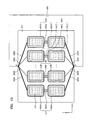
- FIG. 1 illustrates a schematic plan view of a mother substrate for a flat panel display apparatus according to an embodiment
- FIG. 2 illustrates a cross-sectional view of the mother substrate taken along line II-II of FIG. 1 ;
- FIG. 3 illustrates a cross-sectional view of the mother substrate taken along line III-III of FIG. 1 ;
- FIG. 4 illustrates a cross-sectional view of the mother substrate taken along line IV-IV of FIG. 1 ;
- FIG. 5 illustrates an enlarged view showing a part X of FIG. 2 ;
- FIG. 6 illustrates a schematic plan view of a process of applying power from a power source to form a sealing member during manufacturing of the mother substrate of FIG. 1 ;
- FIG. 7 illustrates a schematic plan view of a mother substrate for a flat panel display apparatus according to another embodiment
- FIG. 8 illustrates a cross-sectional view of the mother substrate taken along line VIII-VIII of FIG. 7 ;
- FIG. 9 illustrates a cross-sectional view of the mother substrate taken along line IX-IX of FIG. 7 ;
- FIG. 10 illustrates a schematic plan view of a mother substrate for a flat panel display apparatus according to yet another embodiment
- FIG. 11 illustrates a schematic plan view showing a process of applying power from a power source to form a sealing member during manufacturing of the flat panel display apparatus of FIG. 10 ;
- FIG. 12 illustrates a schematic plan view of a mother substrate for a flat panel display apparatus according to still another embodiment
- FIG. 13 illustrates a schematic plan view illustrating a process of applying power from a power source to form a sealing member during manufacturing of the mother substrate of FIG. 12 ;
- FIG. 14 illustrates a schematic plan view of a mother substrate for a flat panel display apparatus according to still another embodiment
- FIG. 15 illustrates a schematic plan view illustrating a process of applying power from a power source to form a sealing member during manufacturing of the mother substrate of FIG. 14 ;
- FIG. 16 illustrates a schematic plan view of a mother substrate for a flat panel display apparatus according to still another embodiment.
- FIG. 17 illustrates a schematic plan view illustrating a process of applying power from a power source to form a sealing member during manufacturing of the mother substrate of FIG. 16 .
- FIG. 1 illustrates a schematic plan view of a mother substrate 100 for a flat panel display apparatus according to an embodiment.
- FIG. 2 illustrates a cross-sectional view of the mother substrate 100 taken along line II-II of FIG. 1 .
- FIG. 3 illustrates a cross-sectional view of the mother substrate 100 taken along line III-III of FIG. 1 .
- FIG. 4 illustrates a cross-sectional view of the mother substrate 100 taken along line IV-IV of FIG. 1 .
- FIG. 5 illustrates an enlarged view showing a part X of FIG. 2 .
- sealing substrates 102 are not shown for the convenience of explanation.
- the mother substrate 100 for the flat panel display apparatus may include a substrate 101 , display units 110 , the sealing substrates 102 , wiring units 150 , sealing members 170 , connecting units 160 , and inlets 180 .
- the substrate 101 may be formed of, e.g., a glass material including silicon oxide (SiO 2 ) or a transparent plastic material.
- the material for forming the substrate 101 is not limited to the above example, and the substrate 101 may be formed of a transparent plastic material.
- the substrate 101 may include a plastic material e.g., an organic material including at least one of polyethersulfone (PES), polyacrylate (PAR), polyetherimide (PEI), polyethyelenene napthalate (PEN), polyethyeleneterepthalate (PET), polyphenylene sulfide (PPS), polyallylate, polyimide, polycarbonate (PC), cellulose tri-acetate (TAC), and cellulose acetate propionate (CAP).
- PES polyethersulfone
- PAR polyacrylate
- PEI polyetherimide
- PEN polyethyelenene napthalate
- PET polyethyeleneterepthalate
- PPS polyphenylene sulfide
- PPS polyallylate, polyimide, polycarbonate (PC), cellulose tri-acetate (TAC), and cellulose acetate propionate (CAP).
- the display units 110 may be disposed on the substrate 101 .
- Each of the display units 110 may respectively form a flat panel display apparatus.
- FIG. 1 illustrates two display units 110 , and thus, two flat panel display apparatuses may be finally fabricated using the mother substrate 100 of the present embodiment.
- the display unit 110 may be variously formed.
- the display unit 110 may include an organic light-emitting display device.
- the display unit 110 may include a liquid crystal display device.
- the sealing substrate 102 may face the display unit 110 .
- the sealing member 170 may be between the substrate 101 and the sealing substrate 102 .
- the sealing member 170 may surround each of the display units 110 .
- the sealing member 170 may facilitate coupling of the substrate 101 and the sealing substrate 102 .
- the sealing member 170 may include, e.g., frit.
- Each of the wiring units 150 may overlap the sealing member 170 .
- the wiring unit 150 may surround each of the display units 110 .
- the wiring unit 150 may be formed on the substrate 101
- the sealing member 170 may be formed on the wiring unit 150
- the sealing substrate 102 may be disposed on the sealing member 170 .
- the wiring unit 150 may be formed of various conductive materials.
- the wiring units 150 may be arranged in one direction (Y-direction of FIG. 1 ), and the connecting units 160 may be disposed between the wiring units 150 .
- Each of the connecting units 160 may connect adjacent wiring units 150 to each other.
- the connecting unit 160 may include a conductive material, which may be the same as the material of the wiring unit 150 .
- a width “b” of the connecting unit 160 may be greater than a width “a” of the wiring unit 150 .
- a voltage may be applied to the wiring unit 150 .
- the voltage may be applied from an external power source via the inlet 180 to the wiring unit 150 . Therefore, electric current may flow through each of the wiring units 150 , in particular, in the upper wiring unit 150 of the two wiring units 150 illustrated in FIG. 1 . Current flowing through a left portion of the upper wiring unit 150 and current flowing through a right portion of the upper wiring unit 150 may meet at the connecting unit 160 . Then, the current may flow through left and right portions of the lower wiring unit 150 of the two wiring units 150 again.
- a voltage required to generate heat for a melting operation when the sealing member 170 is formed may be applied to the wiring unit 150 .
- a greater load than that in the wiring unit 150 may be generated in the connecting unit 160 .
- twice the heat of the wiring unit 150 may be generated by the connecting unit 160 , and thus, the connecting unit 160 may be damaged.
- the connecting unit 160 of the present embodiment may have a width greater than that of the wiring unit 150 so that excessive heat may not be generated.
- the width of the connecting unit 160 may be about twice the width of the wiring unit 150 or greater.
- the unit 160 may generate heat similar to the wiring unit 150 .
- the inlet 180 may connect to the wiring unit 150 .
- the inlets 180 may be formed on end portions of the two wiring units 150 illustrated in FIG. 1 .
- An external power source (not illustrated) may be connected to the inlet 180 .
- the voltage may be applied to the wiring unit 150 to generate heat.
- the sealing member 170 may be melted by the heat generated in the wiring unit 150 .
- the sealing member 170 may harden.
- the inlet 180 may be formed of the same material as the wiring unit 150 .
- the inlet 180 may have a width that is greater than the width “a” of the wiring unit 150 .
- the width of the inlet 180 may be about twice the width or greater than the width “a” of the wiring unit 150 .
- the heat generated from the inlet 180 may be adjusted to be similar to the heat generated from the wiring unit 150 , like the connecting unit 160 .
- the display unit 110 may be variously formed and, in an implementation, the display unit 110 may include an organic light-emitting device.
- the display unit 110 will be described below in detail with reference to FIG. 5 .
- a buffer layer 111 may be formed on the substrate 101 .
- the buffer layer 111 may provide a flat surface on an upper portion of the substrate 101 and may prevent moisture and impurities from infiltrating into the substrate 101 .
- An active layer 112 may be formed on the buffer layer 111 in a predetermined pattern.
- the active layer 112 may be formed of an inorganic semiconductor, e.g., amorphous silicon or poly silicon, or an organic semiconductor, and may include a source region, a drain region, and a channel region.
- the source and drain regions may be formed by doping the active layer 112 formed of the amorphous silicon or polysilicon, e.g., with impurities.
- a group III element e.g., boron (B)
- B boron
- a p-type semiconductor may be formed.
- a group V element e.g., nitrogen (N)
- N nitrogen
- a gate insulating layer 113 may be formed on the active layer 112 and a gate electrode 114 may be formed on a predetermined region on the gate insulating layer 113 .
- the gate insulating layer 113 is may insulate the active layer 112 and the gate electrode 114 from each other and may be formed of an organic material or an inorganic material, e.g., SiN x and SiO 2 .
- the gate electrode 114 may be formed of a metal or a metal alloy, e.g., Au, Ag, Cu, Ni, Pt, Pd, Al, Mo, an alloy of Al:Nd, or an alloy of Mo:W.
- the material for forming the gate electrode 114 is not limited to the above examples, and various suitable materials may be used in consideration of adherence, flatness, electrical resistance, and processability.
- the gate electrode 114 may be connected to a gate line (not shown) via which electrical signals are applied.
- An interlayer dielectric 115 may be formed on an upper portion of the gate electrode 114 .
- the interlayer dielectric 115 and the gate insulating layer 113 may expose the source and drain regions of the active layer 112 .
- a source electrode 116 and a gate electrode 117 may contact the exposed source and drain regions of the active layer 112 .
- the source electrode 116 and the drain electrode 117 may be formed of a material including, e.g., Au, Pd, Pt, Ni, Rh, Ru, Ir, or Os, and an alloy of two or more metals, e.g., Al, Mo, Al:Nd alloy, or MoW alloy; however, the embodiments are not limited to the above examples.
- a passivation layer 118 may cover the source and drain electrodes 116 and 117 .
- the passivation layer 118 may include an inorganic insulating layer and/or an organic insulating layer.
- the inorganic insulating layer may include, e.g., SiO 2 , SiNx, SiON, Al 2 O 3 , TiO 2 , Ta 2 O 5 , HfO 2 , ZrO 2 , BST, or PZT.
- the organic insulating layer may include, e.g., general universal polymers (PMMA or PS), polymer derivatives including a phenol group, acryl-based polymers, imide-based polymers, aryl ether-based polymers, amide-based polymer, p-xylene based polymers, vinyl alcohol based polymers, and combinations thereof.
- the passivation layer 118 may be formed as a multiple stacked layer including the inorganic and organic insulating layers.
- the passivation layer 118 may expose the drain electrode 117 and an organic light-emitting device 120 may connect to the exposed drain electrode 117 .
- the organic light-emitting device 120 may include a first electrode 121 , a second electrode 122 , and an intermediate layer 123 .
- the first electrode 121 and the drain electrode 117 may contact each other.
- the intermediate layer 123 may include an organic emission layer and may emit visible rays when a voltage is applied thereto through the first and second electrodes 121 and 122 .
- a pixel defining layer 119 may be formed on the first electrode 121 with an insulating material.
- a predetermined opening may be formed in the pixel defining layer 119 to expose the first electrode 121 .
- the intermediate layer 123 may be formed on the exposed first electrode 121 .
- the second electrode 122 may connect to the intermediate layer 123 .
- the first and second electrodes 121 and 122 may have polarities of an anode electrode and a cathode electrode, respectively. However, the polarities of the first and second electrodes 121 and 122 may be changed.
- the sealing substrate 102 may be disposed on the second electrode 122 .
- a cutting process for each of the display units 110 may be finally performed to manufacture the flat panel display apparatuses.
- two flat panel display apparatuses may be obtained from the mother substrate 100 illustrated in FIG. 1 .
- FIG. 6 illustrates a schematic plan view of a process of applying power from a power source to form the sealing member 170 during manufacturing of the mother substrate 100 of FIG. 1 .
- forming the sealing member 170 may include providing a material for forming the sealing member 170 and then melting and hardening the material.
- both terminals of a power source 190 may be connected to the inlets 180 . Then, when the voltage is applied to the inlets 180 , Joule heat may be generated from the wiring units 150 . Thus, the material for forming the sealing member 170 , which may overlap the wiring unit 150 , may be melted. Then, the material may harden to form the sealing member 170 .
- the sealing member 170 may facilitate coupling of the substrate 101 and the sealing substrate 102 .
- the width “b” of the connecting unit 160 may be about twice the width of the wiring unit 150 or greater so as to adjust the heat generated from the connecting unit 160 and thereby prevent the connecting unit 160 from being damaged by the heat. Therefore, the current may constantly flow through each of the wiring units 150 surrounding the display units 110 . Thus, the heat may be constantly generated from each of the wiring units 150 .
- the sealing member 170 may evenly melt and harden, thereby improving a sealing property of the mother substrate 100 for forming the flat panel display apparatus.
- FIG. 7 illustrates a schematic plan view of a mother substrate 200 for forming a flat panel display apparatus according to another embodiment.
- FIG. 8 illustrates a cross-sectional view of the mother substrate 200 taken along line VIII-VIII of FIG. 7 .
- FIG. 9 illustrates a cross-sectional view of the mother substrate 200 taken along line IX-IX of FIG. 7 .
- the mother substrate 200 for forming a flat panel display apparatus may include a substrate 201 , display units 210 , a sealing substrate 202 , wiring units 250 , a protective layer 255 , sealing members 270 , a connecting unit 260 , and inlets 280 .
- a substrate 201 the substrate 201
- display units 210 the display units 210
- a sealing substrate 202 the sealing substrate 202
- wiring units 250 the wiring units 250
- a protective layer 255 for sealing members 270
- sealing members 270 may be described.
- the display units 210 may be disposed on the substrate 201 . Each of the display units 210 may form a flat panel display apparatus. In FIG. 7 , two display units 210 are illustrated. Thus, two flat panel display apparatuses may be fabricated from the mother substrate 200 of the present embodiment.
- the sealing substrate 202 may face the display units 210 .
- the sealing members 270 may be disposed between the substrate 201 and the sealing substrate 202 .
- the sealing members 270 may surround the display units 210 .
- the wiring units 250 may overlap the sealing members 270 . That is, the wiring units 250 may also surround the display units 210 .
- the protective layer 255 may be disposed between the wiring units 250 and the sealing members 270 . That is, the wiring units 250 may be formed on the substrate 201 , the sealing members 270 may be formed on the sealing substrate 202 , and then, the protective layer 255 may be disposed between the wiring units 250 and the sealing members 270 . The protective layer 255 may improve adherence or adhesion between the wiring units 250 and the sealing members 270 .
- the protective layer 255 may also be disposed on the inlets 280 so as to prevent the inlets 280 from being oxidized by moisture and air.
- the protective layer 255 may include an insulating material, e.g., an oxide.
- the wiring units 250 may be arranged in a direction (Y-direction in FIG. 7 ), and the connecting unit 260 may be disposed between the wiring units 250 .
- the connecting unit 260 may connect adjacent wiring units 250 to each other.
- a width “b” of the connecting unit 260 may be greater than a width “a” of the wiring units 250 .
- the inlets 280 may connect to the wiring units 250 .
- the inlets 280 may be formed on end portions of the two wiring units 250 illustrated in FIG. 7 .
- An external power source (not illustrated) may be connected to the inlets 280 .
- the inlets 280 may have widths greater than widths of the wiring units 250 .
- the width of the inlet 280 may be twice the width of the wiring unit 250 or greater.
- each of the display units 210 may be performed to thereby fabricate the flat panel display apparatuses.
- two flat panel display apparatuses may be obtained from the mother substrate 200 illustrated in FIG. 7 .
- forming the sealing members 270 may include providing a material for forming the sealing members 270 and then melting and hardening the material.
- both terminals of a power source may be connected to the inlets 280 . Then, when the voltage is applied to the inlets 280 , the wiring units 250 may generate Joule heat. Thus, the material for forming the sealing member 270 , which may overlap the wiring unit 250 , may be easily melted. Then, the material may harden to form the sealing members 270 .
- the protective layer 255 may be disposed between the wiring units 250 and the sealing members 270 to improve adherence between the wiring units 250 and the sealing members 270 and to improve coupling between the substrate 201 and the sealing substrate 202 .
- the protective layer 255 may be formed on upper portions of the inlets 280 so as to prevent the inlets 280 from being damaged.
- sealing property of the mother substrate 200 for forming a flat panel display apparatus may be improved.
- FIG. 10 illustrates a schematic plan view of a mother substrate 300 for forming a flat panel display apparatus according to yet another embodiment. For convenience of explanation, components that are different from those of the previous embodiments will be described.
- the mother substrate 300 for forming a flat panel display apparatus may include the substrate 101 , display units 310 , a sealing substrate (not illustrated), first through fourth wiring unit groups 351 , 352 , 353 , and 354 , a sealing member (not illustrated), connecting units 360 A, 360 B, 360 C, and 360 D, first through fourth inlets 380 A, 380 B, 380 C, and 380 D, and conductive points P.
- the display units 310 may be disposed on the substrate 301 . Each of the display units 310 may form a flat panel display apparatus.
- the sealing substrate may face the display units 310 .
- the sealing member (not illustrated) may be disposed between the substrate 301 and the sealing substrate. Configurations of the sealing substrate and the sealing member may be the same as those of the previous embodiments and thus, repeated detailed descriptions thereof will not be provided.
- the mother substrate 300 of the present embodiment may include the first wiring unit group 351 , the second wiring unit group 352 , the third wiring unit group 353 , and the fourth wiring unit group 354 .
- the embodiments are not limited thereto; and the mother substrate 300 may include, e.g., five or more wiring unit groups.
- the first wiring unit group 351 may include a plurality of wiring units 350 A arranged in a direction (Y direction of FIG. 10 ) as well as the connecting unit 360 A connecting the wiring units 350 A to each other.
- FIG. 10 two wiring units 350 A and one connecting unit 360 A are illustrated.
- the connecting unit 360 A may have a width greater than a width of the wiring unit 350 A, e.g., the width of the connecting unit 360 A may be about twice the width of the wiring unit 350 A or greater.
- the second wiring unit group 352 may include a plurality of wiring units 350 B arranged in a direction (Y direction of FIG. 10 ) as well as the connecting unit 360 B.
- the connecting unit 360 B may have a width greater than that of the wiring unit 350 B, e.g., about twice the width of the wiring unit 350 B or greater.
- the third wiring unit group 353 may include a plurality of wiring units 350 C arranged in a direction (Y direction of FIG. 10 ) as well as the connecting unit 360 C.
- the connecting unit 360 C may have a width greater than that of the wiring unit 350 C, e.g., about twice the width of the wiring unit 350 C or greater.
- the fourth wiring unit group 354 may include a plurality of wiring units 350 D arranged in a direction (Y direction of FIG. 10 ) as well as a connecting unit 360 D.
- the connecting unit 360 D may have a width greater than that of the wiring unit 350 D, e.g., about twice the width of the wiring unit 350 D or greater.
- the first through fourth wiring unit groups 351 , 352 , 353 , and 354 may be arranged in another direction (X direction of FIG. 10 ) that crosses the direction (Y direction of FIG. 10 ) in which the wiring units are arranged in each group.
- the conductive points P may be disposed above and below, i.e., may face opposite sides of, the first through fourth wiring unit groups 351 , 352 , 353 , and 354 .
- the conductive points P may be connected to an external power source (not illustrated) that may apply a voltage to each of the wiring units during forming of the sealing member (not illustrated).
- the first wiring unit group 351 may be connected to the conductive point P via the first inlet 380 A
- the second wiring unit group 352 may be connected to the conductive point P via the second inlet 380 B
- the third wiring unit group 353 may be connected to the conductive point P via the third inlet 380 C
- the fourth wiring unit group 354 may be connected to the conductive point P via the fourth inlet 380 D.
- Each of the first through fourth inlets 380 A, 380 B, 380 C, and 380 D may include a conductive material so that the voltage applied via the conductive point P may be transmitted to each of the first through fourth wiring unit groups 351 , 352 , 353 , and 354 .
- first through fourth inlets 380 A, 380 B, 380 C, and 380 D may have the same lengths. Therefore, when voltage is supplied via the conductive point P, magnitudes of voltage drops (IR drop) in the first through fourth inlets 380 A, 380 B, 380 C, and 380 D may be controlled to be the same as each other.
- FIG. 11 illustrates a schematic plan view of a process of applying power from a power source to form the sealing member when the mother substrate 300 for forming a flat panel display apparatus is fabricated.
- forming the sealing member may include providing a material for forming the sealing member (not illustrated) and then melting and hardening the material for forming the sealing member.
- both terminals of a power source 390 may be connected to the conductive points P.
- the conductive points P and the first through fourth wiring unit groups 351 , 352 , 353 , and 354 may be connected to each other via the first through fourth inlets 380 A, 380 B, 380 C, and 380 D.
- the power source 390 may apply the voltage to the wiring units 350 A, 350 B, 350 C, and 350 D of the first through fourth wiring unit groups 351 , 352 , 353 , and 354 .
- the first through fourth wiring unit groups 351 , 352 , 353 , and 354 may be separated at different distances from the conductive points P. Thus, there may be a difference between the IR drop in each of the first through fourth wiring unit groups 351 , 352 , 353 , and 354 .
- the lengths of the first through fourth inlets 380 A, 380 B, 380 C, and 380 D may be the same.
- the IR drop in the first through fourth inlets 380 A, 380 B, 380 C, and 380 D may be adjusted to be the same therebetween.
- the voltage may be equally applied to the first through fourth wiring unit groups 351 , 352 , 353 , and 354 , and the wiring units 350 A, 350 B, 350 C, and 350 D may generate heat evenly.
- FIG. 12 illustrates a schematic plan view of a mother substrate 400 for forming a flat panel display apparatus according to still another embodiment. For the convenience of explanation, components that are different from those of the previous embodiments will be described.
- the mother substrate 400 for forming a flat panel display apparatus may include a substrate 401 , display units 510 , a sealing substrate (not illustrated), first through fourth wiring unit groups 451 , 452 , 453 , and 454 , a sealing member (not illustrated), connecting units 460 A, 460 B, 460 C, and 460 D, first through fourth inlets 480 A, 480 B, 480 C, and 480 D, and conductive points P.
- the display units 410 may be disposed on the substrate 401 . Each of the display units 410 may form a flat panel display apparatus.
- the sealing substrate may face the display units 410 .
- the sealing member (not shown) may be disposed between the substrate 401 and the sealing substrate. Configurations of the sealing substrate and the sealing member may be the same as those of the previous embodiments, and thus, repeated detailed descriptions thereof will not be provided.
- the mother substrate 400 of the present embodiment may include the first wiring unit group 451 , the second wiring unit group 452 , the third wiring unit group 453 , and the fourth wiring unit group 454 .
- the embodiments are not limited thereto; and the mother substrate 400 may include, e.g., five or more wiring unit groups.
- the first wiring unit group 451 may include a plurality of wiring units 450 A arranged in a direction (Y direction of FIG. 12 ) as well as the connecting unit 460 A for connecting the wiring units 450 A to each other.
- the connecting unit 460 A may have a width greater than a width of the wiring unit 450 A, e.g., about twice the width of the wiring unit 450 A or greater.
- the second wiring unit group 452 may include a plurality of wiring units 450 B arranged in a direction (Y direction of FIG. 12 ) as well as the connecting unit 460 B for connecting the wiring units 450 B to each other.
- the connecting unit 460 B may have a width greater than that of the wiring unit 450 B, e.g., about twice the width of the wiring unit 450 B or greater.
- the third wiring unit group 453 may include a plurality of wiring units 450 C arranged in a direction (Y direction of FIG. 12 ) as well as the connecting unit 460 C for connecting the wiring units 450 C to each other.
- the connecting unit 460 C may have a width greater than that of the wiring unit 450 C, e.g., about twice the width of the wiring unit 450 C or greater.
- the fourth wiring unit group 454 may include a plurality of wiring units 450 D arranged in a direction (Y direction of FIG. 12 ) as well as the connecting unit 460 D for connecting the wiring units 450 D to each other.
- the connecting unit 460 D may have a width greater than that of the wiring unit 450 D, e.g., about twice the width of the wiring unit 450 D or greater.
- the first through fourth wiring unit groups 451 , 452 , 453 , and 454 may be arranged in another direction (X direction of FIG. 12 ) that crosses the direction (Y direction of FIG. 12 ) in which the wiring units are arranged in each group.
- the conductive points P may be disposed above and below, i.e., may face opposite sides of, the first through fourth wiring unit groups 451 , 452 , 453 , and 454 .
- the first wiring unit group 451 may be connected to the conductive point P via the first inlet 480 A
- the second wiring unit group 452 may be connected to the conductive point P via the second inlet 480 B
- the third wiring unit group 453 may be connected to the conductive point P via the third inlet 480 C
- the fourth wiring unit group 454 may be connected to the conductive point P via the fourth inlet 480 D.
- the first through fourth inlets 480 A, 480 B, 480 C, and 480 D may not have the same lengths.
- lengths of the first and fourth inlets 480 A and 480 D respectively connected to the first and fourth wiring unit groups 451 and 454 , which are further from the conductive points P may be longer than lengths of the second and third inlets 480 B and 480 C respectively connected to the second and third wiring unit groups 452 and 453 , which are close to the conductive points P.
- thicknesses of the second and third inlets 480 B and 480 C may be less than thicknesses of the first and fourth inlets 480 A and 480 D. That is, as the length of each of the first through fourth inlets 480 A, 480 B, 480 C, and 480 D is increased, the thickness of the first, second, third, or fourth inlet 480 A, 480 B, 480 C, or 480 D may also increase.
- magnitudes of an IR drop in each of the first through fourth inlets 480 A, 480 B, 480 C, and 480 D when the voltage is applied through the conductive points P may be adjusted to be the same.
- FIG. 13 illustrates a schematic plan view of a process of applying power from a power source to form the sealing member when the mother substrate 400 of FIG. 12 is fabricated.
- forming the sealing member may include providing a material for forming the sealing member (not shown) and then melting and hardening the material for forming the sealing member.
- both terminals of a power source 490 may be connected to the conductive points P, and the conductive points P and the first through fourth wiring unit groups 451 , 452 , 453 , and 454 may be connected to each other via the first through fourth inlets 480 A, 480 B, 480 C, and 480 D.
- the power source 490 may apply power to the wiring units 450 A, 450 B, 450 C, and 450 D of the first through fourth wiring units groups 451 , 452 , 453 , and 454 .
- first through fourth wiring unit groups 451 , 452 , 453 , and 454 may be separated from the conductive points P by different distances, lengths of the first through fourth inlets 480 A, 480 B, 480 C, and 480 D may be different from each other. Thus, there may be a difference between the IR drops in the first through fourth inlets 480 A, 480 B, 480 C, and 480 D.
- the thickness of the first, second, third, or fourth inlet 480 A, 480 B, 480 C, or 480 D may be increased as the length of the first, second, third, or fourth inlet 480 A, 480 B, 480 C, or 480 D is increased so as to constantly adjust the voltage drop in each of the first through fourth inlets 480 A, 480 B, 480 C, and 480 D.
- heat generated from the wiring units 450 A, 450 B, 450 C, and 450 D may be controlled to be equal to each other.
- FIG. 14 illustrates a schematic plan view of a mother substrate 500 for forming a flat panel display apparatus according to still another embodiment. Components that are different from those of the previous embodiments will be described.
- the mother substrate 500 for forming a flat panel display apparatus may include a substrate 501 , display units 510 , a sealing substrate (not shown), first through fourth wiring unit groups 551 , 552 , 553 , and 554 , a sealing member (not shown), connecting units 560 A, 560 B, 560 C, and 560 D, first through fourth inlets 580 A, 580 B, 580 C, and 580 D, and conductive points P.
- the display units 510 may be disposed on the substrate 501 . Each of the display units 510 may form a flat panel display apparatus.
- the sealing substrate may face the display units 510 .
- the sealing member (not shown) may be between the substrate 501 and the sealing substrate (not shown). Configurations of the sealing substrate and the sealing member may be the same as those of the previous embodiments, and thus, repeated detailed descriptions thereof will not be provided.
- the mother substrate 500 of the present embodiment may include the first wiring unit group 551 , the second wiring unit group 552 , the third wiring unit group 553 , and the fourth wiring unit groups 554 .
- the embodiments are not limited thereto; and the mother substrate may include, e.g., five or more wiring unit groups.
- the first wiring unit group 551 may include a plurality of wiring units 550 A that are arranged in a direction (Y direction of FIG. 14 ) as well as the connecting unit 560 A.
- the connecting unit 560 A may have a width that is greater than that of the wiring unit 550 A, e.g., about twice the width of the wiring unit 550 A or greater.
- the second wiring unit group 552 may include a plurality of wiring units 550 B that are arranged in a direction (Y direction of FIG. 14 ) as well as the connecting unit 560 B.
- the connecting unit 560 B may have a width that is greater than that of the wiring unit 550 B, e.g., about twice the width of the wiring unit 550 B or greater.
- the third wiring unit group 553 may include a plurality of wiring units 550 C that are arranged in a direction (Y direction of FIG. 14 ) as well as the connecting unit 560 C.
- the connecting unit 560 C may have a width that is greater than that of the wiring unit 550 C, e.g., about twice the width of the wiring unit 550 C or greater.
- the fourth wiring unit group 554 may include a plurality of wiring units 550 D that are arranged in a direction (Y direction of FIG. 14 ) as well as the connecting unit 560 D.
- the connecting unit 560 D may have a width that is greater than that of the wiring unit 550 D, e.g., about twice the width of the wiring unit 550 D or greater.
- the first through fourth wiring unit groups 551 , 552 , 553 , and 554 may be arranged in another direction (X direction in FIG. 14 ) crossing the direction in which the wiring units are arranged in each of the first through fourth wiring groups 551 , 552 , 553 , and 554
- the conductive points P may be disposed above and below, i.e., may face opposite sides of, the first through fourth wiring unit groups 551 , 552 , 553 , and 554 .
- the first wiring unit group 551 may be connected to the conductive point P via the first inlet 580 A
- the second wiring unit group 552 may be connected to the conductive point P via the second inlet 580 B
- the third wiring unit group 553 may be connected to the conductive point P via the third inlet 580 C
- the fourth wiring unit group 554 may be connected to the conductive point P via the fourth inlet 580 D.
- the first through fourth inlets 580 A, 580 B, 580 C, and 580 D may not have the same lengths.
- lengths of the first and fourth inlets 580 A and 580 D respectively connected to the first and fourth wiring unit groups 551 and 554 , which are further from the conductive points P may be longer than lengths of the second and third inlets 580 B and 580 C respectively connected to the second and third wiring unit groups 552 and 553 , which are closer to the conductive points P.
- widths of the second and third inlets 580 B and 580 C may be less than widths of the first and fourth inlets 580 A and 580 D.
- widths of the first and fourth inlets 580 A and 580 D may also increase.
- each of the first through fourth inlets 580 A, 580 B, 580 C, and 580 D may have a constant width from an end connected to each of the first through fourth wiring unit groups 551 , 552 , 553 , and 554 and to the other end connected to the conductive point P.
- the embodiments are not limited thereto; and each of the first through fourth inlets 580 A, 580 B, 580 C, and 580 D may have a variable width.
- a width per unit length of each of the through fourth inlets 580 A, 580 B, 580 C, and 580 D may be defined as an average width of each of the through fourth inlets 580 A, 580 B, 580 C, and 580 D, and the average width of each of the first through fourth inlets 580 A, 580 B, 580 C, and 580 D may be increased as the length of the first, second, third, or fourth inlet 580 A, 580 B, 580 C, or 580 D is increased.
- magnitudes of voltage drops (IR drop) in the first through fourth inlets 580 A, 580 B, 580 C, and 580 D may be controlled to be equal to each other when like voltages are applied via the conductive points P to the first through fourth wiring unit groups 551 , 552 , 553 , and 554 .
- FIG. 15 illustrates a schematic plan view of a process of applying power from a power source to form the sealing member when the mother substrate 500 of FIG. 14 is fabricated.
- forming the sealing member may include providing a material for forming the sealing member (not shown) and then melting and hardening the material for forming the sealing member.
- both terminals of a power source 590 may be connected to the conductive points P; and the conductive points P and the first through fourth wiring unit groups 551 , 552 , 553 , and 554 may be connected to each other via the first through fourth inlets 580 A, 580 B, 580 C, and 580 D.
- the power source 590 may apply voltages to the wiring units 550 A, 550 B, 550 C, and 550 D of the first through fourth wiring unit groups 551 , 552 , 553 , and 554 .
- first through fourth wiring unit groups 551 , 552 , 553 , and 554 may be separated from the conductive points P by different distances, the lengths of the first through fourth inlets 580 A, 580 B, 580 C, and 580 D may be different from each other. Thus, there may be a difference between the IR drops in the first through fourth inlets 580 A, 580 B, 580 C, and 580 D.
- the width of the first, second, third, or fourth inlet 580 A, 580 B, 580 C, or 580 D may be increased as the length of the first, second, third, or fourth inlet 580 A, 580 B, 580 C, or 580 D is increased so as to constantly adjust the voltage drop in each of the first through fourth inlets 580 A, 580 B, 580 C, and 580 D.
- the same voltage may be applied to each of the first through fourth wiring unit groups 551 , 552 , 553 , and 554 .
- the heat generated from the wiring units 550 A, 550 B, 550 C, and 550 D may be adjusted to be equal to each other.
- FIG. 16 illustrates a schematic plan view of a mother substrate 600 for forming a flat panel display apparatus according to still another embodiment. For the convenience of explanation, components that are different from those of the previous embodiments will be described.
- the mother substrate 600 for forming a flat panel display apparatus may include a substrate 601 , display units 610 , a sealing substrate (not shown), first through fourth wiring unit groups 651 , 652 , 653 , and 654 , a sealing member (not shown), connecting units 660 A, 660 B, 660 C, and 660 D, first through fourth branching lines 691 A, 691 B, 691 C, and 691 D, an extension unit 692 including first through fourth extension units 692 A, 692 B, 692 C, and 692 D, a center unit 693 , and conductive points P.
- the display units 610 may be disposed on the substrate 601 . Each of the display units 610 may form a flat panel display apparatus.
- the sealing substrate may face the display units 610 .
- the sealing member (not shown) may be disposed between the substrate 601 and the sealing substrate (not shown). Configurations of the sealing substrate and the sealing member may be the same as those of previous embodiments, and thus, repeated detailed descriptions thereof will not be provided.
- the mother substrate 600 of the present embodiment may include the first wiring unit group 651 , the second wiring unit group 652 , the third wiring unit group 653 , and the fourth wiring unit groups 654 .
- the embodiments are not limited thereto; and the mother substrate 600 may include, e.g., five or more wiring unit groups.
- the first wiring unit group 651 may include a plurality of wiring units 650 A that are arranged in a direction (Y direction of FIG. 16 ) as well as the connecting unit 660 A for connecting the wiring units 650 A to each other.
- the connecting unit 660 A may have a width that is greater than that of the wiring unit 650 A, e.g., about twice the width of the wiring unit 650 A or greater.
- the second wiring unit group 652 may include a plurality of wiring units 650 B that are arranged in a direction (Y direction of FIG. 16 ) as well as the connecting unit 660 B for connecting the wiring units 650 B to each other.
- the connecting unit 660 B may have a width that is greater than that of the wiring unit 650 B, e.g., about twice the width of the wiring unit 650 B or greater.
- the third wiring unit group 653 may include a plurality of wiring units 650 C that are arranged in a direction (Y direction of FIG. 16 ) as well as the connecting unit 660 C for connecting the wiring units 650 C to each other.
- the connecting unit 660 C may have a width that is greater than that of the wiring unit 650 C, e.g., about twice the width of the wiring unit 650 C or greater.
- the fourth wiring unit group 654 may include a plurality of wiring units 650 D that are arranged in a direction (Y direction of FIG. 16 ) as well as the connecting unit 660 D for connecting the wiring units 650 D to each other.
- the connecting unit 660 D may have a width that is greater than that of the wiring unit 650 D, e.g., about twice the width of the wiring unit 650 D or greater.
- the first through fourth wiring unit groups 651 , 652 , 653 , and 654 may be arranged in another direction (X direction in FIG. 16 ) crossing the direction in which the wiring units are arranged in each of the first through fourth wiring groups 651 , 652 , 653 , and 654 .
- the conductive points P may be disposed above and below, i.e., may face opposite sides of, the first through fourth wiring unit groups 651 , 652 , 653 , and 654 .
- the first through fourth wiring unit groups 651 , 652 , 653 , and 654 and the conductive points P may be connected to each other via the first through fourth branching lines 691 A, 691 B, 691 C, and 691 D, as will be described in more detail below.
- the first through fourth branching lines 691 A, 691 B, 691 C, and 691 D may be formed at end portions of the first through fourth wiring unit groups 651 , 652 , 653 , and 654 .
- the first branching line 691 A may be formed at the end portion of the first wiring unit group 651
- the second branching line 691 B may be formed at the end portion of the second wiring unit group 652
- the third branching line 691 C may be formed at the end portion of the third wiring unit group 653
- the fourth branching line 691 D may be formed at the end portion of the fourth wiring unit group 654 .
- the first through fourth extension units 692 A, 692 B, 692 C, and 692 D of the extension unit 692 may connect to end portions of the first through fourth branching lines 691 A, 691 B, 691 C, and 691 D.
- the first through fourth extension units 692 A, 692 B, 692 C, and 692 D and the conductive points P may be connected to each other via the center portions 693 .
- the extension unit 692 may include the first extension unit 692 A between the first and second branching lines 691 A and 691 B, the second extension unit 692 B between the second branching line 691 B and the center unit 693 , the third extension unit 692 C between the center unit 693 and the third branching line 691 C, and the fourth extension unit 692 D between the third and fourth branching lines 691 C and 691 D.
- the first inlet between the conductive point P and the first wiring unit group 651 may include the first branching line 691 A, the first extension unit 692 A, the second extension unit 692 B, and the center unit 693 .
- the second inlet between the conductive point P and the second wiring unit group 652 may include the second branching line 691 B, the second extension unit 692 B, and the center unit 693 .
- the third inlet between the conductive point P and the third wiring unit group 653 may include the third branching line 691 C, the third extension unit 692 C, and the center unit 693 .
- the fourth inlet between the conductive point P and the fourth wiring unit group 654 may include the fourth branching line 691 D, the fourth extension unit 692 D, the third extension unit 692 C, and the center unit 693 .
- a width of each of the first through fourth extension units 692 A, 692 B, 692 C, and 692 D may be less the further the first through fourth extension unit 692 A, 692 B, 692 C, and 692 D are from the center unit 693 .
- widths of the second and third extension units 692 B and 692 C may be greater than widths of the first and fourth extension units 692 A and 692 D.
- a power source may apply power to the first through fourth wiring unit groups 650 A, 650 B, 650 C, and 650 D via the conductive points P, the center units 693 , the first through fourth extension units 692 A, 692 B, 692 C, and 692 D, and the first through fourth branching lines 691 A, 691 B, 691 C, and 691 D so that electric current flows through the first through fourth wiring unit groups 650 A, 650 B, 650 C, and 650 D.
- the current flowing through the first branching line 691 A may flow through the first extension unit 692 A
- the current flowing through the first and second branching lines 691 A and 691 B may flow through the second extension units 692 B.
- the current flowing through the fourth branching line 691 D may flow through the fourth extension unit 692 D
- the current flowing through the third and fourth branching lines 691 C and 691 D may flow through the third extension unit 692 C.
- loads that are greater than those of the first and fourth extension units 692 A and 692 D may be applied to the second and third extension units 692 B and 692 C that are closer to the center unit 693 . Therefore, the second and third extension units 692 B and 692 C may generate more heat and current of a desired amount may not flow through the second and third extension units 692 B and 692 C or the second and third extension units 692 B and 692 C may be damaged.
- the width of each of the first, second, third, or fourth extension units 692 A, 692 B, 692 C, and 692 D may be reduced the further the first through fourth extension units 692 A, 692 B, 692 C, and 692 D are from the center unit 693 . That is, the widths of the second and third extension units 692 B and 692 C may be greater than those of the first and fourth extension units 692 A and 692 D. Therefore, the first through fourth extension units 692 A, 692 B, 692 C, and 692 D may generate heat evenly.
- the center unit 693 that is connected to the extension unit 692 may have a width greater than that of each of the first through fourth extension units 692 A, 692 B, 692 C, and 692 D of the extension unit 692 . Therefore, it may be easy to adjust the heat generated from the center unit 693 to be equal to the heat generated from the extension unit 692 .
- the first through fourth branching lines 691 A, 691 B, 691 C, and 691 D, the extension unit 692 , and the center unit 693 may include a conductive material, e.g., a material having low resistivity, such as copper, so that a magnitude of a voltage drop may be reduced.
- a conductive material e.g., a material having low resistivity, such as copper, so that a magnitude of a voltage drop may be reduced.
- FIG. 17 illustrates a schematic plan view of a process of applying power from a power source to form the sealing member when the mother substrate 600 of FIG. 16 is fabricated.
- forming the sealing member may include providing a material for forming the sealing member (not shown) and then melting and hardening the material for forming the sealing member.
- both terminals of a power source 690 may be connected to the conductive points P; and the conductive points P and the first through fourth wiring unit groups 651 , 652 , 653 , and 654 may be connected to each other via the center units 693 , the extension units 692 , and the first through fourth branching lines 691 A, 691 B, 691 C, and 691 D.
- the power source 690 may apply voltage to the first through fourth wiring units 650 A, 650 B, 650 C, and 650 D in the first through fourth wiring unit groups 651 , 652 , 653 , and 654 .
- the width of each of the first through fourth extension units 692 A, 692 B, 692 C, and 692 D may be reduced the further the first through fourth extension unit 692 A, 692 B, 692 C, and 692 D are from the center unit 693 .
- the widths of the second and third extension units 692 B and 692 C may be greater than the widths of the first and fourth extension units 692 A and 692 D so as to control heat generated from the first through fourth extension units 692 A, 692 B, 692 C, and 692 D to be equal to each other and to prevent the first through fourth extension units 692 A, 692 B, 692 C, and 692 D from being damaged by the heat.
- the width of the center unit 693 connected to the extension unit 692 may be greater than that of each of the first through fourth extension units 692 A, 692 B, 692 C, and 692 D of the extension unit 692 .
- the current may flow evenly through the first through fourth wiring units 650 A, 650 B, 650 C, and 650 D surrounding the display units 610 , and accordingly, the sealing member (not shown) may evenly melt and harden.
- the sealing property of the mother substrate 600 for forming a flat panel display apparatus may be improved.
- a mother substrate for forming a flat panel display apparatus and a method of manufacturing the mother substrate a sealing property of the mother substrate may be improved.
- the quality of the flat panel display apparatus may be largely affected by a sealing property of the flat panel display apparatus; and the sealing property, in turn, may depend on the sealing substrate and the sealing member. It may be easy, however, to form the sealing member, which limits the ability to improve the sealing property of the flat panel display apparatus. In the embodiments disclosed, however, such limitations are surmounted and, in particular, the embodiments facilitate forming the sealing member, and thus improve the sealing property of the flat panel display apparatus.
Landscapes
- Engineering & Computer Science (AREA)
- Microelectronics & Electronic Packaging (AREA)
- Physics & Mathematics (AREA)
- Optics & Photonics (AREA)
- Electroluminescent Light Sources (AREA)
Abstract
Description
Claims (22)
Applications Claiming Priority (2)
| Application Number | Priority Date | Filing Date | Title |
|---|---|---|---|
| KR10-2010-0051967 | 2010-06-01 | ||
| KR1020100051967A KR101137393B1 (en) | 2010-06-01 | 2010-06-01 | Mother substrate for flat panel display apparatus and method of manufacturing the same |
Publications (2)
| Publication Number | Publication Date |
|---|---|
| US20110291118A1 US20110291118A1 (en) | 2011-12-01 |
| US8847484B2 true US8847484B2 (en) | 2014-09-30 |
Family
ID=45021343
Family Applications (1)
| Application Number | Title | Priority Date | Filing Date |
|---|---|---|---|
| US13/064,809 Active 2032-10-21 US8847484B2 (en) | 2010-06-01 | 2011-04-18 | Mother substrate for flat panel display apparatus and method of manufacturing the same |
Country Status (2)
| Country | Link |
|---|---|
| US (1) | US8847484B2 (en) |
| KR (1) | KR101137393B1 (en) |
Cited By (1)
| Publication number | Priority date | Publication date | Assignee | Title |
|---|---|---|---|---|
| US20140312765A1 (en) * | 2010-06-15 | 2014-10-23 | Ensil Tech Co., Ltd. | Flat panel display apparatus, mother substrate for flat panel display apparatuses, method of manufacturing the flat panel display apparatus, and method of manufacturing the mother substrate |
Families Citing this family (3)
| Publication number | Priority date | Publication date | Assignee | Title |
|---|---|---|---|---|
| KR102000709B1 (en) * | 2012-08-31 | 2019-09-30 | 삼성디스플레이 주식회사 | Manufacturing method of a display panel |
| KR101973163B1 (en) * | 2016-03-22 | 2019-04-29 | 삼성디스플레이 주식회사 | Display device |
| KR20220000440A (en) * | 2020-06-25 | 2022-01-04 | 삼성디스플레이 주식회사 | Display device and method of fabricating the same |
Citations (13)
| Publication number | Priority date | Publication date | Assignee | Title |
|---|---|---|---|---|
| US5805117A (en) * | 1994-05-12 | 1998-09-08 | Samsung Electronics Co., Ltd. | Large area tiled modular display system |
| JP2000252058A (en) | 1999-03-01 | 2000-09-14 | Stanley Electric Co Ltd | Organic EL display device element and sealing method thereof |
| KR20010109011A (en) | 2000-06-01 | 2001-12-08 | 박원석 | A Method For Fabricating An Organic Electro-Luminescence Display Panel Using A Glass Paste And An Organic Electro-Luminescence Display Panel Thereof |
| KR20010111846A (en) | 2000-06-13 | 2001-12-20 | 권상직 | Method for the low temperature vacuum in-line frit sealing of flat panel display device using an auxiliary heat line |
| KR20030080895A (en) | 2002-04-11 | 2003-10-17 | 엘지전자 주식회사 | Sealing method of organic electroluminescence device |
| KR20060028212A (en) | 2004-09-24 | 2006-03-29 | 전자부품연구원 | Organic electroluminescent device and manufacturing method thereof |
| KR20060079615A (en) | 2005-01-03 | 2006-07-06 | 오리온전기 주식회사 | Organic light emitting device encapsulation method |
| KR20070038312A (en) | 2005-10-05 | 2007-04-10 | 엘지전자 주식회사 | Organic electroluminescent display and manufacturing method |
| US20070096631A1 (en) * | 2005-11-01 | 2007-05-03 | Un-Cheol Sung | Flat panel display and fabricating method thereof |
| KR100761162B1 (en) | 2005-12-26 | 2007-09-21 | 엘지전자 주식회사 | EL display |
| KR100840090B1 (en) | 2007-08-17 | 2008-06-20 | 삼성에스디아이 주식회사 | Organic electroluminescent display and its mother substrate |
| US20090218932A1 (en) | 2008-02-29 | 2009-09-03 | Wenchao Wang | Frit sealing of large device |
| US20090218320A1 (en) | 2008-02-29 | 2009-09-03 | Wenchao Wang | Frit sealing using direct resistive heating |
-
2010
- 2010-06-01 KR KR1020100051967A patent/KR101137393B1/en active Active
-
2011
- 2011-04-18 US US13/064,809 patent/US8847484B2/en active Active
Patent Citations (14)
| Publication number | Priority date | Publication date | Assignee | Title |
|---|---|---|---|---|
| US5805117A (en) * | 1994-05-12 | 1998-09-08 | Samsung Electronics Co., Ltd. | Large area tiled modular display system |
| JP2000252058A (en) | 1999-03-01 | 2000-09-14 | Stanley Electric Co Ltd | Organic EL display device element and sealing method thereof |
| KR20010109011A (en) | 2000-06-01 | 2001-12-08 | 박원석 | A Method For Fabricating An Organic Electro-Luminescence Display Panel Using A Glass Paste And An Organic Electro-Luminescence Display Panel Thereof |
| KR20010111846A (en) | 2000-06-13 | 2001-12-20 | 권상직 | Method for the low temperature vacuum in-line frit sealing of flat panel display device using an auxiliary heat line |
| KR20030080895A (en) | 2002-04-11 | 2003-10-17 | 엘지전자 주식회사 | Sealing method of organic electroluminescence device |
| KR20060028212A (en) | 2004-09-24 | 2006-03-29 | 전자부품연구원 | Organic electroluminescent device and manufacturing method thereof |
| KR20060079615A (en) | 2005-01-03 | 2006-07-06 | 오리온전기 주식회사 | Organic light emitting device encapsulation method |
| KR20070038312A (en) | 2005-10-05 | 2007-04-10 | 엘지전자 주식회사 | Organic electroluminescent display and manufacturing method |
| US20070096631A1 (en) * | 2005-11-01 | 2007-05-03 | Un-Cheol Sung | Flat panel display and fabricating method thereof |
| KR100761162B1 (en) | 2005-12-26 | 2007-09-21 | 엘지전자 주식회사 | EL display |
| KR100840090B1 (en) | 2007-08-17 | 2008-06-20 | 삼성에스디아이 주식회사 | Organic electroluminescent display and its mother substrate |
| US20090045732A1 (en) | 2007-08-17 | 2009-02-19 | Won-Kyu Kwak | Organic light emitting display and mother substrate thereof |
| US20090218932A1 (en) | 2008-02-29 | 2009-09-03 | Wenchao Wang | Frit sealing of large device |
| US20090218320A1 (en) | 2008-02-29 | 2009-09-03 | Wenchao Wang | Frit sealing using direct resistive heating |
Non-Patent Citations (1)
| Title |
|---|
| Korean Notice of Allowance in KR 10-2010-0051967, dated Mar. 27, 2012 (Kwon, et al.). |
Cited By (1)
| Publication number | Priority date | Publication date | Assignee | Title |
|---|---|---|---|---|
| US20140312765A1 (en) * | 2010-06-15 | 2014-10-23 | Ensil Tech Co., Ltd. | Flat panel display apparatus, mother substrate for flat panel display apparatuses, method of manufacturing the flat panel display apparatus, and method of manufacturing the mother substrate |
Also Published As
| Publication number | Publication date |
|---|---|
| US20110291118A1 (en) | 2011-12-01 |
| KR101137393B1 (en) | 2012-04-20 |
| KR20110132128A (en) | 2011-12-07 |
Similar Documents
| Publication | Publication Date | Title |
|---|---|---|
| CN107221550B (en) | display device | |
| CN100580948C (en) | Flat panel display device | |
| US20210011536A1 (en) | Semiconductor device | |
| CN104637438B (en) | Flexible display and its manufacturing method | |
| US9159946B2 (en) | Organic light emitting diode display having auxiliary electrode | |
| US7883921B2 (en) | Thin film transistor array panel and manufacturing method thereof | |
| US8680767B2 (en) | Flat panel display apparatus, mother substrate for flat panel display apparatuses, method of manufacturing the flat panel display apparatus, and method of manufacturing the mother substrate | |
| EP2475009B1 (en) | Method of manufacturing an organic light emitting display device | |
| CN106527816A (en) | Touch substrate, preparation method thereof and touch display device | |
| US20130300283A1 (en) | Flat panel display and method of manufacturing the same | |
| US8847484B2 (en) | Mother substrate for flat panel display apparatus and method of manufacturing the same | |
| KR20190047365A (en) | Oxide semiconductor thin film transistor and method of manufacturing the same | |
| US20150123114A1 (en) | Thin film transistor array panel and method for manufacturing the same | |
| CN105051908A (en) | Thin film transistor array | |
| US20040188681A1 (en) | [pixel structure] | |
| US20150144951A1 (en) | Thin film transistor array panel and manufacturing method thereof | |
| US20130033834A1 (en) | Flat Panel Display Apparatus, Mother Substrate for Flat Panel Display Apparatus, Method of Manufacturing Flat Panel Display Apparatus, and Method of Manufacturing Mother Substrate for Flat Panel Display Apparatus | |
| US20090213039A1 (en) | Display device | |
| US8564197B2 (en) | Flat panel display apparatus and method for manufacturing the same | |
| KR101808432B1 (en) | Oxide semiconductor thin film transistor and method of manufacturing the same | |
| US20120224342A1 (en) | Flat Panel Display Apparatus, Mother Substrate for Flat Panel Display Apparatus, Method of Manufacturing the Flat Panel Display Apparatus, and Method of Manufacturing the Mother Substrate for the Flat Panel Display Apparatus | |
| KR101741687B1 (en) | Flat panel display apparatus and method of manufacturing the same | |
| CN101958401B (en) | Organic electroluminescence element and manufacturing method thereof | |
| KR101810052B1 (en) | Flat panel display apparatus and method of manufacturing flat panel display apparatus | |
| US20120105413A1 (en) | Flat panel display apparatus and method of manufacturing flat panel display apparatus |
Legal Events
| Date | Code | Title | Description |
|---|---|---|---|
| AS | Assignment |
Owner name: SAMSUNG MOBILE DISPLAY CO., LTD., KOREA, REPUBLIC Free format text: ASSIGNMENT OF ASSIGNORS INTEREST;ASSIGNORS:KWON, OH-SEOB;KOH, SUNG-SOO;HAN, BYUNG-UK;AND OTHERS;REEL/FRAME:026241/0125 Effective date: 20110331 |
|
| AS | Assignment |
Owner name: ENSIL TECH CO., LTD., KOREA, REPUBLIC OF Free format text: ASSIGNMENT OF ASSIGNORS INTEREST;ASSIGNOR:SAMSUNG MOBILE DISPLAY CO., LTD.;REEL/FRAME:026902/0531 Effective date: 20110907 Owner name: ENSIL TECH CO., LTD., KOREA, REPUBLIC OF Free format text: CORRECTIVE ASSIGNMENT TO CORRECT THE ASSIGNEE'S OWNERSHIP INTEREST TO 50% PREVIOUSLY RECORDED ON REEL 026902 FRAME 0531. ASSIGNOR(S) HEREBY CONFIRMS THE ASSIGNMENT;ASSIGNOR:SAMSUNG MOBILE DISPLAY CO., LTD.;REEL/FRAME:026903/0006 Effective date: 20110907 |
|
| AS | Assignment |
Owner name: SAMSUNG DISPLAY CO., LTD., KOREA, REPUBLIC OF Free format text: MERGER;ASSIGNOR:SAMSUNG MOBILE DISPLAY CO., LTD.;REEL/FRAME:029096/0174 Effective date: 20120827 |
|
| FEPP | Fee payment procedure |
Free format text: PAYOR NUMBER ASSIGNED (ORIGINAL EVENT CODE: ASPN); ENTITY STATUS OF PATENT OWNER: LARGE ENTITY |
|
| STCF | Information on status: patent grant |
Free format text: PATENTED CASE |
|
| MAFP | Maintenance fee payment |
Free format text: PAYMENT OF MAINTENANCE FEE, 4TH YEAR, LARGE ENTITY (ORIGINAL EVENT CODE: M1551) Year of fee payment: 4 |
|
| MAFP | Maintenance fee payment |
Free format text: PAYMENT OF MAINTENANCE FEE, 8TH YEAR, LARGE ENTITY (ORIGINAL EVENT CODE: M1552); ENTITY STATUS OF PATENT OWNER: LARGE ENTITY Year of fee payment: 8 |
|
| MAFP | Maintenance fee payment |
Free format text: PAYMENT OF MAINTENANCE FEE, 12TH YEAR, LARGE ENTITY (ORIGINAL EVENT CODE: M1553); ENTITY STATUS OF PATENT OWNER: LARGE ENTITY Year of fee payment: 12 |